EP2802068A2 - Rectification synchrone dans des topologies de convertisseur/inverseur à trois niveaux - Google Patents
Rectification synchrone dans des topologies de convertisseur/inverseur à trois niveaux Download PDFInfo
- Publication number
- EP2802068A2 EP2802068A2 EP14167387.1A EP14167387A EP2802068A2 EP 2802068 A2 EP2802068 A2 EP 2802068A2 EP 14167387 A EP14167387 A EP 14167387A EP 2802068 A2 EP2802068 A2 EP 2802068A2
- Authority
- EP
- European Patent Office
- Prior art keywords
- power
- power module
- diode
- turned
- synchronous rectifier
- Prior art date
- Legal status (The legal status is an assumption and is not a legal conclusion. Google has not performed a legal analysis and makes no representation as to the accuracy of the status listed.)
- Withdrawn
Links
Images


Classifications
-
- H—ELECTRICITY
- H02—GENERATION; CONVERSION OR DISTRIBUTION OF ELECTRIC POWER
- H02M—APPARATUS FOR CONVERSION BETWEEN AC AND AC, BETWEEN AC AND DC, OR BETWEEN DC AND DC, AND FOR USE WITH MAINS OR SIMILAR POWER SUPPLY SYSTEMS; CONVERSION OF DC OR AC INPUT POWER INTO SURGE OUTPUT POWER; CONTROL OR REGULATION THEREOF
- H02M3/00—Conversion of DC power input into DC power output
- H02M3/02—Conversion of DC power input into DC power output without intermediate conversion into AC
- H02M3/04—Conversion of DC power input into DC power output without intermediate conversion into AC by static converters
- H02M3/10—Conversion of DC power input into DC power output without intermediate conversion into AC by static converters using discharge tubes with control electrode or semiconductor devices with control electrode
- H02M3/145—Conversion of DC power input into DC power output without intermediate conversion into AC by static converters using discharge tubes with control electrode or semiconductor devices with control electrode using devices of a triode or transistor type requiring continuous application of a control signal
- H02M3/155—Conversion of DC power input into DC power output without intermediate conversion into AC by static converters using discharge tubes with control electrode or semiconductor devices with control electrode using devices of a triode or transistor type requiring continuous application of a control signal using semiconductor devices only
-
- H—ELECTRICITY
- H02—GENERATION; CONVERSION OR DISTRIBUTION OF ELECTRIC POWER
- H02M—APPARATUS FOR CONVERSION BETWEEN AC AND AC, BETWEEN AC AND DC, OR BETWEEN DC AND DC, AND FOR USE WITH MAINS OR SIMILAR POWER SUPPLY SYSTEMS; CONVERSION OF DC OR AC INPUT POWER INTO SURGE OUTPUT POWER; CONTROL OR REGULATION THEREOF
- H02M7/00—Conversion of AC power input into DC power output; Conversion of DC power input into AC power output
- H02M7/02—Conversion of AC power input into DC power output without possibility of reversal
- H02M7/04—Conversion of AC power input into DC power output without possibility of reversal by static converters
- H02M7/12—Conversion of AC power input into DC power output without possibility of reversal by static converters using discharge tubes with control electrode or semiconductor devices with control electrode
- H02M7/21—Conversion of AC power input into DC power output without possibility of reversal by static converters using discharge tubes with control electrode or semiconductor devices with control electrode using devices of a triode or transistor type requiring continuous application of a control signal
- H02M7/217—Conversion of AC power input into DC power output without possibility of reversal by static converters using discharge tubes with control electrode or semiconductor devices with control electrode using devices of a triode or transistor type requiring continuous application of a control signal using semiconductor devices only
-
- H—ELECTRICITY
- H02—GENERATION; CONVERSION OR DISTRIBUTION OF ELECTRIC POWER
- H02M—APPARATUS FOR CONVERSION BETWEEN AC AND AC, BETWEEN AC AND DC, OR BETWEEN DC AND DC, AND FOR USE WITH MAINS OR SIMILAR POWER SUPPLY SYSTEMS; CONVERSION OF DC OR AC INPUT POWER INTO SURGE OUTPUT POWER; CONTROL OR REGULATION THEREOF
- H02M7/00—Conversion of AC power input into DC power output; Conversion of DC power input into AC power output
- H02M7/42—Conversion of DC power input into AC power output without possibility of reversal
- H02M7/44—Conversion of DC power input into AC power output without possibility of reversal by static converters
- H02M7/48—Conversion of DC power input into AC power output without possibility of reversal by static converters using discharge tubes with control electrode or semiconductor devices with control electrode
- H02M7/483—Converters with outputs that each can have more than two voltages levels
- H02M7/487—Neutral point clamped inverters
-
- H—ELECTRICITY
- H02—GENERATION; CONVERSION OR DISTRIBUTION OF ELECTRIC POWER
- H02M—APPARATUS FOR CONVERSION BETWEEN AC AND AC, BETWEEN AC AND DC, OR BETWEEN DC AND DC, AND FOR USE WITH MAINS OR SIMILAR POWER SUPPLY SYSTEMS; CONVERSION OF DC OR AC INPUT POWER INTO SURGE OUTPUT POWER; CONTROL OR REGULATION THEREOF
- H02M7/00—Conversion of AC power input into DC power output; Conversion of DC power input into AC power output
- H02M7/42—Conversion of DC power input into AC power output without possibility of reversal
- H02M7/44—Conversion of DC power input into AC power output without possibility of reversal by static converters
- H02M7/48—Conversion of DC power input into AC power output without possibility of reversal by static converters using discharge tubes with control electrode or semiconductor devices with control electrode
- H02M7/53—Conversion of DC power input into AC power output without possibility of reversal by static converters using discharge tubes with control electrode or semiconductor devices with control electrode using devices of a triode or transistor type requiring continuous application of a control signal
- H02M7/537—Conversion of DC power input into AC power output without possibility of reversal by static converters using discharge tubes with control electrode or semiconductor devices with control electrode using devices of a triode or transistor type requiring continuous application of a control signal using semiconductor devices only, e.g. single switched pulse inverters
- H02M7/5387—Conversion of DC power input into AC power output without possibility of reversal by static converters using discharge tubes with control electrode or semiconductor devices with control electrode using devices of a triode or transistor type requiring continuous application of a control signal using semiconductor devices only, e.g. single switched pulse inverters in a bridge configuration
- H02M7/53871—Conversion of DC power input into AC power output without possibility of reversal by static converters using discharge tubes with control electrode or semiconductor devices with control electrode using devices of a triode or transistor type requiring continuous application of a control signal using semiconductor devices only, e.g. single switched pulse inverters in a bridge configuration with automatic control of output voltage or current
-
- Y—GENERAL TAGGING OF NEW TECHNOLOGICAL DEVELOPMENTS; GENERAL TAGGING OF CROSS-SECTIONAL TECHNOLOGIES SPANNING OVER SEVERAL SECTIONS OF THE IPC; TECHNICAL SUBJECTS COVERED BY FORMER USPC CROSS-REFERENCE ART COLLECTIONS [XRACs] AND DIGESTS
- Y02—TECHNOLOGIES OR APPLICATIONS FOR MITIGATION OR ADAPTATION AGAINST CLIMATE CHANGE
- Y02B—CLIMATE CHANGE MITIGATION TECHNOLOGIES RELATED TO BUILDINGS, e.g. HOUSING, HOUSE APPLIANCES OR RELATED END-USER APPLICATIONS
- Y02B70/00—Technologies for an efficient end-user side electric power management and consumption
- Y02B70/10—Technologies improving the efficiency by using switched-mode power supplies [SMPS], i.e. efficient power electronics conversion e.g. power factor correction or reduction of losses in power supplies or efficient standby modes
Definitions
- the subject invention relates to three level power inverter/converter topologies, and more particularly, to the application of synchronous rectification in a uni-directional active rectifier circuit to reduce static losses by lowering the voltage drop across the circuit utilizing power semiconductor devices.
- Synchronous rectification is a concept that has been applied in the past, particularly in DC-DC converters at low output voltage levels.
- a voltage drop of 0.4 V to about 1.0 V in the output rectifier is common and would be converted into a significant loss, since the output voltage of a typical DC-DC power converter is usually only about 1.0 or 2.0 V.
- Synchronous rectification involves the use of a power FET connected in parallel with a diode, wherein the FET is configured to be turned on when the diode is conducting, so that current flow is re-directed through the FET. Since the FET operates with lower resistance than the diode, the voltage drop across the circuit will be lower and more efficient.
- the subject invention is directed to a new and useful power module, such as a three-level inverter/converter, employing synchronous rectification to reduce static losses and enhance efficiency.
- the power module includes a first synchronous rectifier switch (containing a first FET) that communicates with a positive DC terminal of the power module.
- the first synchronous rectifier switch is connected in parallel with a first diode. Together, the first synchronous rectifier switch and the first diode form a first module block, which comprises a first synchronous rectifier of the power module.
- the power module further includes a second power FET connected in parallel with a second diode to form a second module block, and a third power FET is connected in parallel with a third diode to form a third module block.
- the second and third module blocks are positioned between first and second terminal interfaces (IO1 and I02) of the power module, and two serially connected diodes are utilized on the first (IO1) terminal interface side of the power module in parallel with the serially connected second and third module blocks.
- a second synchronous rectifier switch (containing a fourth FET) communicates with a second (102) terminal of the power module.
- the switch is connected in parallel with a fourth diode to form a fourth module block.
- the second synchronous rectifier switch and the fourth diode form a fourth module block, which comprises a second synchronous rectifier of the power module.
- a synchronous rectifier is also connected in parallel with each of the serially connected diodes on the first (IO1) terminal interface side of the power module.
- each synchronous rectifier switch comprises a silicon carbide (SiC) power MOSFET connected in parallel with an internal inherent power diode.
- each diode that is connected in parallel with a synchronous rectifier is a silicon carbide (SiC) Shottky diode.
- the power module further includes a current sensor for sensing current flowing through the first diode and the fourth diode. More preferably, the power module includes a current sensor located in the circuit for sensing current flowing through the parallel connected first synchronous rectifier switch and first diode (i.e., the first module block), and for sensing current flowing through the parallel connected fourth synchronous rectifier switch and fourth diode (i.e., the fourth module block).
- control logic is provided to control the operation of the synchronous rectifiers of the power module.
- the first and second synchronous rectifiers are configured so that they are not turned on while the second and third power FETs are turned on.
- the second and third power FETs are configured to be turned on simultaneously.
- the first and second synchronous rectifiers are configured so that they are turned on at different times. More particularly, the first and second synchronous rectifiers (i.e., the first and fourth module blocks) are configured so that they are turned on at different parts of two half-cycles.
- the first synchronous rectifier switch is configured so that it is turned on only after the first diode has conducted current and then turned off before the current through the first diode has completely stopped. Moreover, the first synchronous rectifier switch is configured so that it is not turned on as the same time as the second and thirds power FETs are turned on, to prevent a shoot-through condition.
- the second synchronous rectifier switch is configured so that it is turned on only after the fourth diode has conducted current and then turned off before the current through the fourth diode has completely stopped. Moreover, the second synchronous rectifier switch is configured so that it is not turned on at the same time as the second and third power FETs are turned on, to prevent a shoot-through condition.
- Fig. 1 a schematic representation of a prior art uni-directional Vienna-type active rectifier, which serves as precursor topology for the power module of the subject invention.
- a prior art Vienna-type active rectifier includes two power MOSFET devices at the center of the circuit.
- FIG. 2 An exemplary embodiment of a power module constructed in accordance with a preferred embodiment of the subject invention is illustrated in Fig. 2 .
- the power module of Fig. 2 is configured as part of a three-level power inverter/converter and is adapted for use in a unidirectional active rectifier mode.
- the power module of the subject invention employs a plurality of synchronous rectifiers each consisting of a silicon carbide (SiC) power MOSFET connected in parallel with a SiC Schottky power diode.
- SiC silicon carbide
- FET and MOSFET should not be construed in a manner so as to limit the subject invention in any way. Rather, it should be understood by those skilled in the art that the circuits shown and described herein could be constructed and applied with other types of power FET devices known in the art, including, for example, JFET devices, DMOSFET devices and CoolMOS devices.
- the power module includes a first synchronous rectifier switch S 1 D 1 that communicates with a first terminal of the power module.
- the first terminal of the module is a positive DC terminal.
- the first synchronous rectifier switch S 1 D 1 is connected in parallel with a first reverse-parallel SiC Schottky diode SBD 1 to form the first synchronous rectifier block.
- the power module further includes a second power FET S 2 D 2 that is connected in parallel with a second reverse-parallel SiC Schottky diode SBD 2 , and a third power FET S 3 D 3 that is connected in parallel with a third SiC Shottky diode SBD 3 .
- the second and third power FETs S 2 D 2 and S 3 D 3 are positioned between first and second terminal interfaces 10 1 and 10 2 of the power module.
- Two serially connected fast switching Schottky diodes SBD Z1 and SBD Z2 are utilized on the first terminal interface side IO 1 of the power module connected in parallel with the serially connected second and third power FETs S 2 D 2 and S 3 D 3 .
- the power module of Fig. 2 further includes a second synchronous rectifier switch S 4 D 4 that connects with a second terminal of the power module.
- the second terminal of the power module is a negative DC terminal.
- the second synchronous rectifier switch S 4 D 4 is connected in parallel with a fourth diode SBD 4 which is a reverse-parallel SiC Schottky diode, forming a second synchronous rectifier block.
- the first and second synchronous rectifier switches S 1 D 1 and S 4 D 4 are configured so that they are not turned on while the second and third power FETs S 2 D 2 and S 3 D 3 are turned on.
- the second and third power FETs S 2 D 2 and S 3 D 3 are configured to be turned on simultaneously.
- the SiC Schottky diode SBD 1 is turned on "naturally" (since it is forward-biased). Once it is confirmed that SBD 1 is turned on and after a short dead-time delay, the first synchronous rectifier switch S 1 D 1 can be turned on, lowering the voltage across the SiC Schottky diode SBD 1 significantly.
- the first and second synchronous rectifiers switches S 1 D 1 and S 4 D 4 are configured so that they are turned on at different times. More particularly, the first and second synchronous rectifier switches S 1 D 1 and S 4 D 4 are configured so that they are turned on at different parts of two half-cycles. Since these synchronous rectifiers effectively operate like low resistance components, the voltage drop in the SiC Schottky diodes SBD 1 and SBD 4 is controllably reduced. Furthermore, forward diode voltage will decrease in portion to the die size of the FET used in the rectification.
- the first synchronous rectifier switch S 1 D 1 is configured so that it is turned on only after the first diode SBD 1 has conducted current and then turned off before the current through the first diode SBD 1 has completely stopped. Moreover, the first synchronous rectifier switch S 1 D 1 is configured so that it is turned on not at the same time when the second and third power FETs S 2 D 2 and S 3 D 3 are turned on to prevent a shoot-through condition.
- the second synchronous rectifier switch S 4 D 4 is configured so that it is turned on only after the fourth diode SBD 4 has conducted current and then turned off before the current through the fourth diode SBD 4 has completely stopped. Moreover, the second synchronous rectifier switch S 4 D 4 is configured so that it is turned on not at the same time when the second and third power FETs S 2 D 2 and S 3 D 3 rectifiers are turned on to prevent a shoot-through condition.
- the power module of Fig. 2 further includes means for sensing current flowing through the first Schottky diode SBD 1 and the second Schottky diode SBD 4 . More preferably, the power module includes means for sensing current flowing through the parallel connected first synchronous rectifier switch S 1 D 1 and first Schottky diode SBD 1 , and for sensing current flowing through the parallel connected second synchronous rectifier switch S 4 D 4 and second Schottky diode SBD 4 .
- control logic is provided to control the operation of the synchronous rectifiers of the power module shown in Fig. 2 . More particularly, control logic is employed to turn the synchronous rectification on and off during the operation of the power module.
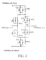
- FIG. 3 there is shown another power module constructed in accordance with a preferred embodiment of the subject invention.
- a synchronous rectifier is also connected in parallel with each of the serially connected diodes SBD Z1 and SBD Z2 on the first terminal interface side of the power module.
- a similar switching logic to that employed with the power module described with respect to Fig. 1 could also be applied and this topology, for both the three-level inverter and converter.
- SiC Schottky diodes utilized in the power module of the subject invention, have a much lower reverse recovery current than silicon fast recovery diodes, and a higher reverse voltage, thus the SiC Schottky diode is very fast at the turn-on and turn-off times.
- the forward voltage drop through the SiC Schottky diode is relatively high (up to 1.7 V max) as compared to the voltage drop of a large die-size SiC power MOSFET.
- the synchronous rectifier (as a combination of a SiC MOSFET and SiC Schottky diode), a good rectification device for high frequency and high power operation (fast turn-on, turn-off and low conduction drop, translates to high efficiency at a high operating frequency).
- silicon carbide has a high thermal conductivity, and temperature has little influence on its switching and thermal characteristics.
- silicon carbide Schottky diodes can operate at junction temperatures of over 500 K (about 200 °C), which allows passive radiative cooling in aerospace applications such as those disclosed herein.
Landscapes
- Engineering & Computer Science (AREA)
- Power Engineering (AREA)
- Rectifiers (AREA)
- Inverter Devices (AREA)
- Dc-Dc Converters (AREA)
Applications Claiming Priority (1)
| Application Number | Priority Date | Filing Date | Title |
|---|---|---|---|
| US13/888,935 US9172301B2 (en) | 2013-05-07 | 2013-05-07 | Synchronous rectification in the three-level inverter-converter topologies |
Publications (2)
| Publication Number | Publication Date |
|---|---|
| EP2802068A2 true EP2802068A2 (fr) | 2014-11-12 |
| EP2802068A3 EP2802068A3 (fr) | 2015-09-09 |
Family
ID=50639373
Family Applications (1)
| Application Number | Title | Priority Date | Filing Date |
|---|---|---|---|
| EP14167387.1A Withdrawn EP2802068A3 (fr) | 2013-05-07 | 2014-05-07 | Rectification synchrone dans des topologies de convertisseur/inverseur à trois niveaux |
Country Status (2)
| Country | Link |
|---|---|
| US (1) | US9172301B2 (fr) |
| EP (1) | EP2802068A3 (fr) |
Cited By (3)
| Publication number | Priority date | Publication date | Assignee | Title |
|---|---|---|---|---|
| WO2016170569A1 (fr) * | 2015-04-20 | 2016-10-27 | 東芝三菱電機産業システム株式会社 | Convertisseur et dispositif de conversion de puissance utilisant ce convertisseur |
| CN111642061A (zh) * | 2020-06-01 | 2020-09-08 | 西安交通大学 | 一种Vienna整流用双面结构碳化硅功率模块及其制备方法 |
| CN113991989A (zh) * | 2021-12-27 | 2022-01-28 | 深圳市永联科技股份有限公司 | 电流纹波调整单元及相关产品 |
Families Citing this family (10)
| Publication number | Priority date | Publication date | Assignee | Title |
|---|---|---|---|---|
| US9362844B2 (en) * | 2013-06-14 | 2016-06-07 | Hamilton Sundstrand Corporation | Method of deriving switch current signals in a rectifier |
| US9672582B2 (en) * | 2014-12-05 | 2017-06-06 | Toyota Motor Engineering & Manufacturing North America, Inc. | Systems and methods for Gaussian filter standard deviation variation |
| JP6610406B2 (ja) * | 2016-04-19 | 2019-11-27 | 株式会社デンソー | 電力変換装置 |
| CN106981998A (zh) * | 2017-04-07 | 2017-07-25 | 南京航空航天大学 | 一种可拓宽调制比逆变器及其调制策略 |
| US10193544B2 (en) * | 2017-04-21 | 2019-01-29 | Ford Global Technologies, Llc | Minimizing ringing in wide band gap semiconductor devices |
| CN108462399A (zh) * | 2018-01-11 | 2018-08-28 | 浙江大学 | 一种高效整流器 |
| CN110323954B (zh) * | 2019-08-08 | 2020-11-03 | 中车青岛四方车辆研究所有限公司 | 基于SiC功率器件的三电平牵引功率模块及逆变电路 |
| EP4315584A4 (fr) * | 2021-04-21 | 2024-05-22 | Huawei Digital Power Technologies Co., Ltd. | Convertisseur de puissance |
| JP7550730B2 (ja) * | 2021-07-02 | 2024-09-13 | 三菱電機株式会社 | 半導体装置、半導体モジュール、及び、電力変換装置 |
| CN114465455A (zh) * | 2021-07-07 | 2022-05-10 | 厦门三优光电股份有限公司 | 不加反并联续流二极管的全SiC功率模块 |
Citations (1)
| Publication number | Priority date | Publication date | Assignee | Title |
|---|---|---|---|---|
| EP2237402A1 (fr) * | 2008-01-31 | 2010-10-06 | Daikin Industries, Ltd. | Transformateur de puissance |
Family Cites Families (8)
| Publication number | Priority date | Publication date | Assignee | Title |
|---|---|---|---|---|
| US6256214B1 (en) * | 1999-03-11 | 2001-07-03 | Ericsson Inc. | General self-driven synchronous rectification scheme for synchronous rectifiers having a floating gate |
| US6188592B1 (en) * | 1999-11-05 | 2001-02-13 | Ericsson Inc. | Externally-driven scheme for synchronous rectification |
| TW548892B (en) * | 2000-11-30 | 2003-08-21 | Delta Electronics Inc | Synchronous rectification circuit |
| US7375988B2 (en) * | 2005-03-08 | 2008-05-20 | Wall Industries, Inc. | Self-synchronized high voltage synchronous rectifier and drive |
| TWM301461U (en) * | 2006-05-09 | 2006-11-21 | Hipro Electronics Taiwan Co Lt | Half-bridge LLC resonant transformer having a synchronizing rectifying function |
| US8582331B2 (en) | 2009-07-20 | 2013-11-12 | Vincotech Holdings S.à.r.l. | Inverter topologies usable with reactive power |
| WO2012056766A1 (fr) | 2010-10-27 | 2012-05-03 | 三菱電機株式会社 | Appareil de conversion électrique |
| CA2778072C (fr) | 2011-05-27 | 2015-12-01 | Alstom Technology Ltd. | Methode de determination de modele de controle de npc vsc, plus particulierement comme filtre d'alimentation actif |
-
2013
- 2013-05-07 US US13/888,935 patent/US9172301B2/en active Active
-
2014
- 2014-05-07 EP EP14167387.1A patent/EP2802068A3/fr not_active Withdrawn
Patent Citations (1)
| Publication number | Priority date | Publication date | Assignee | Title |
|---|---|---|---|---|
| EP2237402A1 (fr) * | 2008-01-31 | 2010-10-06 | Daikin Industries, Ltd. | Transformateur de puissance |
Cited By (6)
| Publication number | Priority date | Publication date | Assignee | Title |
|---|---|---|---|---|
| WO2016170569A1 (fr) * | 2015-04-20 | 2016-10-27 | 東芝三菱電機産業システム株式会社 | Convertisseur et dispositif de conversion de puissance utilisant ce convertisseur |
| KR20170136620A (ko) * | 2015-04-20 | 2017-12-11 | 도시바 미쓰비시덴키 산교시스템 가부시키가이샤 | 컨버터 및 그것을 사용한 전력 변환 장치 |
| JPWO2016170569A1 (ja) * | 2015-04-20 | 2018-02-01 | 東芝三菱電機産業システム株式会社 | コンバータおよびそれを用いた電力変換装置 |
| CN111642061A (zh) * | 2020-06-01 | 2020-09-08 | 西安交通大学 | 一种Vienna整流用双面结构碳化硅功率模块及其制备方法 |
| CN111642061B (zh) * | 2020-06-01 | 2021-12-28 | 西安交通大学 | 一种Vienna整流用双面结构碳化硅功率模块及其制备方法 |
| CN113991989A (zh) * | 2021-12-27 | 2022-01-28 | 深圳市永联科技股份有限公司 | 电流纹波调整单元及相关产品 |
Also Published As
| Publication number | Publication date |
|---|---|
| US20140334208A1 (en) | 2014-11-13 |
| EP2802068A3 (fr) | 2015-09-09 |
| US9172301B2 (en) | 2015-10-27 |
Similar Documents
| Publication | Publication Date | Title |
|---|---|---|
| US9172301B2 (en) | Synchronous rectification in the three-level inverter-converter topologies | |
| Gurpinar et al. | Single-phase T-type inverter performance benchmark using Si IGBTs, SiC MOSFETs, and GaN HEMTs | |
| JP5118258B2 (ja) | 電力変換装置 | |
| CN100576707C (zh) | 单向dc-dc变换器 | |
| US9362844B2 (en) | Method of deriving switch current signals in a rectifier | |
| EP1679782A2 (fr) | Dispositif de conversion de tension à base de semiconducteur en GaN | |
| EP2728734A1 (fr) | Onduleur fixé au point neutre à trois niveaux | |
| CN103636113A (zh) | 升降压型ac/dc转换器 | |
| CN103378757B (zh) | 功率转换装置 | |
| CN107078732A (zh) | 使用多个电流决定开关模式操作混合功率器件的方法和系统 | |
| CN108370223A (zh) | 电力转换装置 | |
| EP2811632A1 (fr) | Circuit d'attaque pour élément semi-conducteur de commutation et circuit de conversion électrique l'utilisant | |
| CN106921305B (zh) | 三电平功率转换电路 | |
| JP6136011B2 (ja) | 半導体装置、および電力変換装置 | |
| Todorovic et al. | Sic mw pv inverter | |
| JP4719746B2 (ja) | カスコード整流器 | |
| Garcia-Rodriguez et al. | Design of a GaN-based microinverter for photovoltaic systems | |
| US12573956B2 (en) | Converter for power conversion, three-phase converter arrangement and method for packaging a converter | |
| JP6641782B2 (ja) | 電力変換装置 | |
| JP2016144326A (ja) | 共振型dc−dcコンバータ | |
| EP2858221A1 (fr) | Protection contre les courts-circuits | |
| Alharbi et al. | A highly efficient non-isolated DC-DC buck-boost converter with a cascode GaN-FET and SiC-Schottky diode | |
| EP3057232A1 (fr) | Dispositif de coupe-circuit | |
| CN104521122A (zh) | 逆变驱动电路 | |
| Abbatelli et al. | Fully SiC based high efficiency boost converter |
Legal Events
| Date | Code | Title | Description |
|---|---|---|---|
| PUAI | Public reference made under article 153(3) epc to a published international application that has entered the european phase |
Free format text: ORIGINAL CODE: 0009012 |
|
| 17P | Request for examination filed |
Effective date: 20140507 |
|
| AK | Designated contracting states |
Kind code of ref document: A2 Designated state(s): AL AT BE BG CH CY CZ DE DK EE ES FI FR GB GR HR HU IE IS IT LI LT LU LV MC MK MT NL NO PL PT RO RS SE SI SK SM TR |
|
| AX | Request for extension of the european patent |
Extension state: BA ME |
|
| PUAL | Search report despatched |
Free format text: ORIGINAL CODE: 0009013 |
|
| AK | Designated contracting states |
Kind code of ref document: A3 Designated state(s): AL AT BE BG CH CY CZ DE DK EE ES FI FR GB GR HR HU IE IS IT LI LT LU LV MC MK MT NL NO PL PT RO RS SE SI SK SM TR |
|
| AX | Request for extension of the european patent |
Extension state: BA ME |
|
| RIC1 | Information provided on ipc code assigned before grant |
Ipc: H02M 7/487 20070101ALI20150803BHEP Ipc: H02M 7/217 20060101AFI20150803BHEP Ipc: H02M 7/5387 20070101ALI20150803BHEP |
|
| R17P | Request for examination filed (corrected) |
Effective date: 20160309 |
|
| RBV | Designated contracting states (corrected) |
Designated state(s): AL AT BE BG CH CY CZ DE DK EE ES FI FR GB GR HR HU IE IS IT LI LT LU LV MC MK MT NL NO PL PT RO RS SE SI SK SM TR |
|
| STAA | Information on the status of an ep patent application or granted ep patent |
Free format text: STATUS: EXAMINATION IS IN PROGRESS |
|
| 17Q | First examination report despatched |
Effective date: 20180220 |
|
| STAA | Information on the status of an ep patent application or granted ep patent |
Free format text: STATUS: THE APPLICATION IS DEEMED TO BE WITHDRAWN |
|
| 18D | Application deemed to be withdrawn |
Effective date: 20221008 |