EP2814152A2 - Procédé de dérivation de signaux de courant de commutation dans un redresseur - Google Patents
Procédé de dérivation de signaux de courant de commutation dans un redresseur Download PDFInfo
- Publication number
- EP2814152A2 EP2814152A2 EP14172345.2A EP14172345A EP2814152A2 EP 2814152 A2 EP2814152 A2 EP 2814152A2 EP 14172345 A EP14172345 A EP 14172345A EP 2814152 A2 EP2814152 A2 EP 2814152A2
- Authority
- EP
- European Patent Office
- Prior art keywords
- gate driver
- signal
- signals
- switch
- rectifier
- Prior art date
- Legal status (The legal status is an assumption and is not a legal conclusion. Google has not performed a legal analysis and makes no representation as to the accuracy of the status listed.)
- Granted
Links
Images


Classifications
-
- H—ELECTRICITY
- H02—GENERATION; CONVERSION OR DISTRIBUTION OF ELECTRIC POWER
- H02M—APPARATUS FOR CONVERSION BETWEEN AC AND AC, BETWEEN AC AND DC, OR BETWEEN DC AND DC, AND FOR USE WITH MAINS OR SIMILAR POWER SUPPLY SYSTEMS; CONVERSION OF DC OR AC INPUT POWER INTO SURGE OUTPUT POWER; CONTROL OR REGULATION THEREOF
- H02M7/00—Conversion of AC power input into DC power output; Conversion of DC power input into AC power output
- H02M7/02—Conversion of AC power input into DC power output without possibility of reversal
- H02M7/04—Conversion of AC power input into DC power output without possibility of reversal by static converters
- H02M7/12—Conversion of AC power input into DC power output without possibility of reversal by static converters using discharge tubes with control electrode or semiconductor devices with control electrode
- H02M7/21—Conversion of AC power input into DC power output without possibility of reversal by static converters using discharge tubes with control electrode or semiconductor devices with control electrode using devices of a triode or transistor type requiring continuous application of a control signal
- H02M7/217—Conversion of AC power input into DC power output without possibility of reversal by static converters using discharge tubes with control electrode or semiconductor devices with control electrode using devices of a triode or transistor type requiring continuous application of a control signal using semiconductor devices only
- H02M7/2173—Conversion of AC power input into DC power output without possibility of reversal by static converters using discharge tubes with control electrode or semiconductor devices with control electrode using devices of a triode or transistor type requiring continuous application of a control signal using semiconductor devices only in a biphase or polyphase circuit arrangement
-
- H—ELECTRICITY
- H02—GENERATION; CONVERSION OR DISTRIBUTION OF ELECTRIC POWER
- H02M—APPARATUS FOR CONVERSION BETWEEN AC AND AC, BETWEEN AC AND DC, OR BETWEEN DC AND DC, AND FOR USE WITH MAINS OR SIMILAR POWER SUPPLY SYSTEMS; CONVERSION OF DC OR AC INPUT POWER INTO SURGE OUTPUT POWER; CONTROL OR REGULATION THEREOF
- H02M1/00—Details of apparatus for conversion
- H02M1/08—Circuits specially adapted for the generation of control voltages for semiconductor devices incorporated in static converters
- H02M1/084—Circuits specially adapted for the generation of control voltages for semiconductor devices incorporated in static converters using a control circuit common to several phases of a multi-phase system
-
- H—ELECTRICITY
- H02—GENERATION; CONVERSION OR DISTRIBUTION OF ELECTRIC POWER
- H02M—APPARATUS FOR CONVERSION BETWEEN AC AND AC, BETWEEN AC AND DC, OR BETWEEN DC AND DC, AND FOR USE WITH MAINS OR SIMILAR POWER SUPPLY SYSTEMS; CONVERSION OF DC OR AC INPUT POWER INTO SURGE OUTPUT POWER; CONTROL OR REGULATION THEREOF
- H02M7/00—Conversion of AC power input into DC power output; Conversion of DC power input into AC power output
- H02M7/02—Conversion of AC power input into DC power output without possibility of reversal
- H02M7/04—Conversion of AC power input into DC power output without possibility of reversal by static converters
- H02M7/12—Conversion of AC power input into DC power output without possibility of reversal by static converters using discharge tubes with control electrode or semiconductor devices with control electrode
- H02M7/21—Conversion of AC power input into DC power output without possibility of reversal by static converters using discharge tubes with control electrode or semiconductor devices with control electrode using devices of a triode or transistor type requiring continuous application of a control signal
- H02M7/217—Conversion of AC power input into DC power output without possibility of reversal by static converters using discharge tubes with control electrode or semiconductor devices with control electrode using devices of a triode or transistor type requiring continuous application of a control signal using semiconductor devices only
-
- H—ELECTRICITY
- H02—GENERATION; CONVERSION OR DISTRIBUTION OF ELECTRIC POWER
- H02M—APPARATUS FOR CONVERSION BETWEEN AC AND AC, BETWEEN AC AND DC, OR BETWEEN DC AND DC, AND FOR USE WITH MAINS OR SIMILAR POWER SUPPLY SYSTEMS; CONVERSION OF DC OR AC INPUT POWER INTO SURGE OUTPUT POWER; CONTROL OR REGULATION THEREOF
- H02M1/00—Details of apparatus for conversion
- H02M1/0003—Details of control, feedback or regulation circuits
- H02M1/0009—Devices or circuits for detecting current in a converter
Definitions
- the subject invention relates to synchronous rectification, and more particularly, to a method of deriving the individual switching current signal for the currents flowing in each switch of the synchronous rectifier switches utilized in a three-level Vienna-type active rectifier.
- Synchronous rectification is a concept that has been applied in the past, particularly in DC-DC converters at low output voltage levels.
- a voltage drop of 0.4 V to about 1.0 V in the output rectifier is common and would be converted into a significant loss, since the output voltage of a typical DC-DC power converter in these applications is usually only about 1.0 or 2.0V.
- Synchronous rectification involves the use of a power MOSFET connected in parallel with a diode, wherein the MOSFET is configured to be turned on when the diode is conducting, so that current flow is re-directed through the MOSFET. Since the MOSFET operates with lower resistance than the diode, the voltage drop across the circuit will be lower and more efficient.
- the subject invention is directed to a new and useful method of deriving switch currents in a rectifier that includes the steps of generating gate driver signals and subsequently deriving switch currents from the gate driver signals.
- the method may further include the step of using analog switches driven by the gate driver signals to derive the switch currents.
- the method may also include the step of providing a first analog switch for deriving the top switch current signal, a second analog switch for deriving the clamp switch current signal and a third analog switch for deriving the bottom switch current signal.
- Line current may be sensed upstream from the power switch block of a Vienna-type active rectifier whether a synchronous rectification principle is applied.
- the gate driver signals derived to drive the gates of the power switched are preferably generated by a pulse width modulator and include a top gate driver signal, a clamp gate driver signal and a bottom gate driver signal.
- the top and bottom gate driver signals are delayed with respect to the clamp gate driver signal.
- the step of generating the gate driver signals preferably includes the step of comparing a nearly sinusoidal control signal from a controller with two triangular waveforms.
- the subject invention is also directed to a method of deriving synchronous switch currents signals for a three-phase Vienna-type active rectifier that includes the step of generating gate driver signals for each phase of the rectifier by pulse width modulation, wherein the gate driver signals include a top gate driver signal, a clamp gate driver signal and a bottom gate driver signal.
- the method further includes the step of deriving synchronous switch currents from the gate driver signals and the sensed line current signal (which comes from a current sensor installed in front of the rectifier power semi-conductor switch block), wherein the synchronous switch current signals include a top gate switch current signal, a clamp gate switch current signal and a bottom gate switch current signal.
- the method may further include the step of using analog switches driven by the gate driver signals to derive the individual switch current signals, wherein the analog switches include a first analog switch driven by the driver signal of the top gate to provide the top switch current signal, a second analog switch driven by the driver signal of the clamp gate to provide the clamp switch current signal and a third analog switch driven by the driver signal of the bottom gate to provide the bottom switch current signal.
- the top and bottom gate driver signals are delayed with respect to the clamp gate driver signal.
- SiC synchronous rectifier refers to a combined module block that includes a SiC Schottky diode connected in parallel with a SiC MOSFET.
- the SiC MOSFET is configured to be turned on when the diode is conducting, so that current flow is re-directed through the MOSFET rather than the diode.
- a SiC MOSFET is designed to have very low resistance when it is turned on, and therefore its use leads to a lower voltage drop across the circuit than if only a SiC Schottky diode were used. Consequently, the module conduction loss is significantly reduced, as compared to a conventional rectifier or SiC Schottky diode.
- Fig. 1 a single-phase portion of a three-phase conventional Vienna-type active rectifier.
- the two front-end diodes connected to inductor L are regular diodes.
- the two front end diodes need not be SiC type diodes in normal operating temperatures. Because these are diodes, there is no switching at the front-end of the rectifier.
- the top and bottom diodes should be SiC Schottky diodes. And, for both high frequency and high temperature operating conditions, all four of the diodes, including the two front end diodes as well as the top and bottom diodes should be SiC Schottky diodes. Thus, there is switching in the front end as well as in the top and bottom of the rectifier.
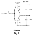
- Fig. 2 there is illustrated a single phase portion of a Vienna-type active rectifier similar to the topology shown in Fig. 1 .
- the top and bottom diodes are replaced by two SiC synchronous rectifiers.
- the two front-end diodes connected to inductor L need not be SiC Schottky type. Instead, these two diodes can be regular diodes that have low voltage drops.
- the top and bottom diodes are provided as two SiC synchronous rectifier blocks (S1 and S2). Within each of these blocks, the SiC MOSFETs are used to further reduce the diode forward voltage drops, while still maintaining the rapid turn-on and turn-off properties of the Schottky SiC diode in the rectifier switch.
- Fig. 3 there is illustrated a single phase portion of a Vienna-type rectifier similar to the topology shown in Fig. 2 .
- the two front end diodes are replaced by SiC synchronous rectifier blocks. This is particularly well adapted for high temperature and high frequency operating conditions.
- the two source-connected synchronous rectifiers i.e., the two blocks that are connected to the source inductor L
- the two source-connected synchronous rectifiers can be fully turned-on during the top-half and bottom-half of the source current half-cycles.
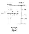
- a basic Y-clamped active rectifier that includes two clamped SiC Schottky diodes (D1 and D2) and a bidirectional switch containing two pairs of SiC Schottky diode and SiC MOSFETs connected in parallel (S1 and S2).
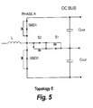
- the Y-clamped active rectifier of Fig. 4 can be modified as shown in Fig. 5 , by replacing the SiC Schottky diodes (D1 and D2) with two SiC MOSFETs that are connected in parallel with SiC Schottky diodes (SBD1 and SBD2).
- the SiC MOSFETs are turned-on after their reverse parallel SiC Schottky diodes are turned-on and then turned-off shortly before their reverse parallel SiC Schottky diodes turned-off.
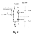
- Fig. 6 there is illustrated a single phase portion of a Vienna-type active rectifier as shown in Fig. 2 , wherein line current is sensed at a location that is next to the switching pole of the circuit, using a single current sensor.
- current signals for the currents flowing inside the diodes (these are also the current signals of the current flowing in the corresponding synchronous rectifiers) of the Vienna-type active rectifier are sensed using a single current sensor for the phase.
- the synchronous switch current signals for S1 and S2 and the clamp switch currents S Clamp 1 and S Clamp 2 of the rectifier can be derived using analog switches driven by derived gate signals, as explained in more detail below.
- the switching pole containing the analog switches for each individual rectifier phase, which includes a first analog switch (Switch 1) for deriving the signal for the current flowing through the top switch of the rectifier phase, a second analog switch (Switch 2) for deriving the signal for the current flowing through the clamp switches of the rectifier phase and a third analog switch (Switch 3) for deriving the signal for the current flowing through the bottom switch of the rectifier phase.
- Line current signal is sensed and fed upstream to the three analog switches.
- the gate driver signals generated by the pulse width modulator (PWM) are fed to the gates of the analog switches of each switching pole of each phase, which include a top gate driver signal, a clamp gate driver signal and a bottom gate driver signal.
- PWM pulse width modulator
- the analog switches When each gate of the analog switches is closed (i.e., logic "1"), it will permit the sensed line current signal (as illustrated in Fig. 6 ) to pass through the analog switch to become a current signal representing the switch current of the corresponding switch of the rectifier, including, for example, the top and bottom synchronous rectifiers shown in the topology of Fig. 2 .
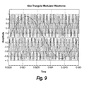
- Fig. 8 there is illustrated a block diagram of a pulse width modulator used to generate the control signals for each phase of the rectifier. That is, the PWM generates a control signal for the top, middle and bottom gates of the active rectifier switches, as shown in Fig. 7 . More particularly, the PWM signals obtained from sine-triangular modulation method are used to drive the three gates of the analog switches of the switching pole.
- Fig. 9 shows an example of a sine-triangle modulation waveform used to create gate driver signals for a Vienna-type active rectifier (although as noted later that the sine-triangular modulation is not the only method to create the PWM signals). This is accomplished by comparing a "nearly" sinusoidal control signal (coming from a controller) with the two triangular waveforms. The amplitude of the sine wave can be up or down. In this example, a modulation frequency of 19.6 kHz and a modulation index of 0.9 at 400 Hz fundamental frequency are illustrated.
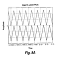
- Fig. 10 there is illustrated the gate driver signals generated by the PWM. It is assumed that a few microseconds of delay exists from the top (or bottom) gate signal relative to the middle clamp gate signal. This delay is sufficient to prevent any shoot-through condition from occurring within the synchronous rectifier switches.
- the clamp switch pair gate driver signal in the plot at the middle of Fig. 10 controls: the two middle switches in Topology A of Fig. 1 ; the two middle switches in Topology B of Fig. 2 ; the two right-side middle switches in Topology C of Fig. 3 ; and the two clamp switches in Topologies D and E of Figs. 4 and 5 .
- the two left-side middle switches in Topology C of Fig. 3 are turned on-and-off differently by the direction of the line source current at tow half-cycles.
- FIG. 11 shows the gate drive signal applied to the top synchronous rectifier switch (lower plot) and the derived signal representing the current flowing in the top synchronous rectifier switch (upper plot);
- Fig. 12 shows the gate driver signal applied to the bottom synchronous rectifier switch (upper plot) and the derived signal representing the current flowing in the bottom synchronous rectifier switch (lower plot);
- Fig. 13 shows the gate driver signal applied to the clamped middle switches (lower plot) and the derived signal representing the current flowing in the clamp middle switches (upper plot).
- a method is disclosed to generate the gate driver signals applied to the top and bottom synchronous rectifier switches of a Vienna-type active rectifier.
- a method is disclosed to use a single current sensor per phase to sense the line current next to the active rectifier switches, to derive the current signals for all rectifier switches. This derivation can be applied in the Vienna-type active rectifiers where synchronous rectifiers are utilized to further reduce the voltage drops across the SiC Schottky diodes.
- the derived switch currents serve to prevent reverse current flow in the synchronous switches, which is prohibited due to unidirectional power flow constraint in aircraft power systems.
Landscapes
- Engineering & Computer Science (AREA)
- Power Engineering (AREA)
- Rectifiers (AREA)
Applications Claiming Priority (1)
| Application Number | Priority Date | Filing Date | Title |
|---|---|---|---|
| US13/918,521 US9362844B2 (en) | 2013-06-14 | 2013-06-14 | Method of deriving switch current signals in a rectifier |
Publications (3)
| Publication Number | Publication Date |
|---|---|
| EP2814152A2 true EP2814152A2 (fr) | 2014-12-17 |
| EP2814152A3 EP2814152A3 (fr) | 2015-04-29 |
| EP2814152B1 EP2814152B1 (fr) | 2021-11-17 |
Family
ID=50933076
Family Applications (1)
| Application Number | Title | Priority Date | Filing Date |
|---|---|---|---|
| EP14172345.2A Active EP2814152B1 (fr) | 2013-06-14 | 2014-06-13 | Procédé de dérivation de signaux de courant de commutation dans un redresseur |
Country Status (2)
| Country | Link |
|---|---|
| US (1) | US9362844B2 (fr) |
| EP (1) | EP2814152B1 (fr) |
Cited By (3)
| Publication number | Priority date | Publication date | Assignee | Title |
|---|---|---|---|---|
| EP3557748A1 (fr) * | 2018-04-19 | 2019-10-23 | Hamilton Sundstrand Corporation | Redressement de ca à tolérance de pannes |
| CN113193768A (zh) * | 2021-04-21 | 2021-07-30 | 三峡大学 | 四开关管串联型的背靠背式三电平整流器 |
| EP4380025A4 (fr) * | 2021-09-28 | 2024-09-25 | Huawei Technologies Co., Ltd. | Procédé de commande de circuit de correction de facteur de puissance (pfc) et circuit de pfc |
Families Citing this family (10)
| Publication number | Priority date | Publication date | Assignee | Title |
|---|---|---|---|---|
| CN104081645A (zh) * | 2012-02-03 | 2014-10-01 | 东芝三菱电机产业系统株式会社 | 功率转换装置 |
| DE102013221322A1 (de) * | 2013-10-21 | 2015-04-23 | Robert Bosch Gmbh | Halbbrücke für einen aktiven Gleichrichter |
| CN103715921B (zh) * | 2013-12-19 | 2015-10-28 | 浙江大学 | 用于vienna整流器的限流控制方法 |
| US9531378B1 (en) | 2015-09-03 | 2016-12-27 | Toyota Motor Engineering & Manufacturing North America, Inc. | Method and apparatus for driving a power device |
| US10630165B2 (en) | 2017-09-08 | 2020-04-21 | General Electric Company | Systems and methods for synchronous power conversion |
| DE102017130498A1 (de) | 2017-12-19 | 2019-06-19 | Dr. Ing. H.C. F. Porsche Aktiengesellschaft | Leistungselektronikmodul für eine Ladestation sowie entsprechende Ladestation und Stromtankstelle |
| US10298118B1 (en) * | 2018-05-14 | 2019-05-21 | Haier Us Appliance Solutions, Inc. | Systems and methods for self-driven active rectification |
| JP7039430B2 (ja) * | 2018-09-19 | 2022-03-22 | 株式会社東芝 | Ac/dcコンバータ |
| CN112865561B (zh) * | 2021-01-28 | 2022-05-06 | 三峡大学 | 一种二极管箝位式背对背无桥三电平整流器 |
| DE102021206853B3 (de) | 2021-06-30 | 2022-02-10 | Vitesco Technologies GmbH | Treiberschaltung mit zwei kaskadierten Halbbrückentreibern zur Ansteuerung von drei Transistoren |
Family Cites Families (9)
| Publication number | Priority date | Publication date | Assignee | Title |
|---|---|---|---|---|
| JP3412067B2 (ja) * | 1997-09-30 | 2003-06-03 | 株式会社日立製作所 | 電力変換装置 |
| JP2002315343A (ja) * | 2001-04-18 | 2002-10-25 | Hitachi Ltd | Pwmコンバータ装置 |
| US20080013352A1 (en) * | 2006-07-13 | 2008-01-17 | Baker Donal E | Active rectifier system with power factor correction |
| US7751212B2 (en) * | 2007-04-23 | 2010-07-06 | Raytheon Company | Methods and apparatus for three-phase rectifier with lower voltage switches |
| US7986538B2 (en) * | 2008-06-03 | 2011-07-26 | Hamilton Sundstrand Corporation | Midpoint current and voltage regulation of a multi-level converter |
| JP5463289B2 (ja) * | 2008-08-22 | 2014-04-09 | 東芝三菱電機産業システム株式会社 | 電力変換装置 |
| US8804388B2 (en) * | 2010-12-06 | 2014-08-12 | Hamilton Sundstrand Corporation | Active rectification control |
| EP2590312A1 (fr) | 2011-11-04 | 2013-05-08 | Alstom Technology Ltd | Convertisseur de source de tension avec topologie clampée en neutre modifiée et procédé de fonctionnement d'un tel convertisseur |
| US9172301B2 (en) * | 2013-05-07 | 2015-10-27 | Hamilton Sundstrand Corporation | Synchronous rectification in the three-level inverter-converter topologies |
-
2013
- 2013-06-14 US US13/918,521 patent/US9362844B2/en active Active
-
2014
- 2014-06-13 EP EP14172345.2A patent/EP2814152B1/fr active Active
Non-Patent Citations (1)
| Title |
|---|
| None |
Cited By (3)
| Publication number | Priority date | Publication date | Assignee | Title |
|---|---|---|---|---|
| EP3557748A1 (fr) * | 2018-04-19 | 2019-10-23 | Hamilton Sundstrand Corporation | Redressement de ca à tolérance de pannes |
| CN113193768A (zh) * | 2021-04-21 | 2021-07-30 | 三峡大学 | 四开关管串联型的背靠背式三电平整流器 |
| EP4380025A4 (fr) * | 2021-09-28 | 2024-09-25 | Huawei Technologies Co., Ltd. | Procédé de commande de circuit de correction de facteur de puissance (pfc) et circuit de pfc |
Also Published As
| Publication number | Publication date |
|---|---|
| EP2814152B1 (fr) | 2021-11-17 |
| US20140369101A1 (en) | 2014-12-18 |
| US9362844B2 (en) | 2016-06-07 |
| EP2814152A3 (fr) | 2015-04-29 |
Similar Documents
| Publication | Publication Date | Title |
|---|---|---|
| US9362844B2 (en) | Method of deriving switch current signals in a rectifier | |
| CN107318272B (zh) | 半导体装置 | |
| CN205725436U (zh) | 栅极驱动电路以及包括栅极驱动电路的桥电路 | |
| EP3103189B1 (fr) | Dispositif onduleur à niveaux multiples et procédé de fonctionnement | |
| EP2728734A1 (fr) | Onduleur fixé au point neutre à trois niveaux | |
| EP2966768A1 (fr) | Onduleur à trois niveaux | |
| US10554150B2 (en) | Three-level inverter | |
| US9172301B2 (en) | Synchronous rectification in the three-level inverter-converter topologies | |
| EP3105846B1 (fr) | Onduleur hybride multi-niveau et procédé de fonctionnement | |
| EP2811632A1 (fr) | Circuit d'attaque pour élément semi-conducteur de commutation et circuit de conversion électrique l'utilisant | |
| Uemura et al. | Comparative evaluation of T-type topologies comprising standard and reverse-blocking IGBTs | |
| Yapa et al. | Analysis of SiC technology in two-level and three-level converters for aerospace applications | |
| US10601303B2 (en) | Control method and device for circuit with a bridge arm of a switch | |
| CN103580526A (zh) | 功率转换装置 | |
| EP2814154A1 (fr) | Procédé de réduction de la distorsion de courant d'entrée dans un redresseur | |
| Todorovic et al. | Sic mw pv inverter | |
| CN105940599A (zh) | 电力变换装置及控制装置 | |
| EP4451542A1 (fr) | Convertisseur arcp et commande de celui-ci | |
| Sanjeev et al. | Analysis of conduction and switching losses in two level inverter for low power applications | |
| EP2936672B1 (fr) | Branche de pont | |
| US10298118B1 (en) | Systems and methods for self-driven active rectification | |
| Mazgaj et al. | A novel soft switching system for three-phase voltage source inverter | |
| JP5857189B2 (ja) | インバータ装置 | |
| EP4482003A1 (fr) | Agencement pour le partage de courant de convertisseurs connectés en parallèle | |
| Zeng et al. | Four-step switching strategy for bidirectional switches in single-phase ac/ac buck converter |
Legal Events
| Date | Code | Title | Description |
|---|---|---|---|
| 17P | Request for examination filed |
Effective date: 20140613 |
|
| AK | Designated contracting states |
Kind code of ref document: A2 Designated state(s): AL AT BE BG CH CY CZ DE DK EE ES FI FR GB GR HR HU IE IS IT LI LT LU LV MC MK MT NL NO PL PT RO RS SE SI SK SM TR |
|
| AX | Request for extension of the european patent |
Extension state: BA ME |
|
| PUAI | Public reference made under article 153(3) epc to a published international application that has entered the european phase |
Free format text: ORIGINAL CODE: 0009012 |
|
| PUAL | Search report despatched |
Free format text: ORIGINAL CODE: 0009013 |
|
| AK | Designated contracting states |
Kind code of ref document: A3 Designated state(s): AL AT BE BG CH CY CZ DE DK EE ES FI FR GB GR HR HU IE IS IT LI LT LU LV MC MK MT NL NO PL PT RO RS SE SI SK SM TR |
|
| AX | Request for extension of the european patent |
Extension state: BA ME |
|
| RIC1 | Information provided on ipc code assigned before grant |
Ipc: H02M 1/084 20060101AFI20150326BHEP |
|
| R17P | Request for examination filed (corrected) |
Effective date: 20151029 |
|
| RBV | Designated contracting states (corrected) |
Designated state(s): AL AT BE BG CH CY CZ DE DK EE ES FI FR GB GR HR HU IE IS IT LI LT LU LV MC MK MT NL NO PL PT RO RS SE SI SK SM TR |
|
| STAA | Information on the status of an ep patent application or granted ep patent |
Free format text: STATUS: EXAMINATION IS IN PROGRESS |
|
| 17Q | First examination report despatched |
Effective date: 20180219 |
|
| RIC1 | Information provided on ipc code assigned before grant |
Ipc: H02M 1/00 20060101ALN20201125BHEP Ipc: H02M 1/084 20060101AFI20201125BHEP |
|
| GRAP | Despatch of communication of intention to grant a patent |
Free format text: ORIGINAL CODE: EPIDOSNIGR1 |
|
| STAA | Information on the status of an ep patent application or granted ep patent |
Free format text: STATUS: GRANT OF PATENT IS INTENDED |
|
| INTG | Intention to grant announced |
Effective date: 20210114 |
|
| GRAJ | Information related to disapproval of communication of intention to grant by the applicant or resumption of examination proceedings by the epo deleted |
Free format text: ORIGINAL CODE: EPIDOSDIGR1 |
|
| STAA | Information on the status of an ep patent application or granted ep patent |
Free format text: STATUS: EXAMINATION IS IN PROGRESS |
|
| GRAP | Despatch of communication of intention to grant a patent |
Free format text: ORIGINAL CODE: EPIDOSNIGR1 |
|
| INTC | Intention to grant announced (deleted) | ||
| STAA | Information on the status of an ep patent application or granted ep patent |
Free format text: STATUS: GRANT OF PATENT IS INTENDED |
|
| RIC1 | Information provided on ipc code assigned before grant |
Ipc: H02M 1/084 20060101AFI20210507BHEP Ipc: H02M 1/00 20060101ALN20210507BHEP |
|
| INTG | Intention to grant announced |
Effective date: 20210610 |
|
| GRAS | Grant fee paid |
Free format text: ORIGINAL CODE: EPIDOSNIGR3 |
|
| GRAA | (expected) grant |
Free format text: ORIGINAL CODE: 0009210 |
|
| STAA | Information on the status of an ep patent application or granted ep patent |
Free format text: STATUS: THE PATENT HAS BEEN GRANTED |
|
| AK | Designated contracting states |
Kind code of ref document: B1 Designated state(s): AL AT BE BG CH CY CZ DE DK EE ES FI FR GB GR HR HU IE IS IT LI LT LU LV MC MK MT NL NO PL PT RO RS SE SI SK SM TR |
|
| REG | Reference to a national code |
Ref country code: GB Ref legal event code: FG4D |
|
| REG | Reference to a national code |
Ref country code: DE Ref legal event code: R096 Ref document number: 602014081268 Country of ref document: DE |
|
| REG | Reference to a national code |
Ref country code: IE Ref legal event code: FG4D |
|
| REG | Reference to a national code |
Ref country code: AT Ref legal event code: REF Ref document number: 1448869 Country of ref document: AT Kind code of ref document: T Effective date: 20211215 |
|
| REG | Reference to a national code |
Ref country code: LT Ref legal event code: MG9D |
|
| REG | Reference to a national code |
Ref country code: NL Ref legal event code: MP Effective date: 20211117 |
|
| REG | Reference to a national code |
Ref country code: AT Ref legal event code: MK05 Ref document number: 1448869 Country of ref document: AT Kind code of ref document: T Effective date: 20211117 |
|
| PG25 | Lapsed in a contracting state [announced via postgrant information from national office to epo] |
Ref country code: RS Free format text: LAPSE BECAUSE OF FAILURE TO SUBMIT A TRANSLATION OF THE DESCRIPTION OR TO PAY THE FEE WITHIN THE PRESCRIBED TIME-LIMIT Effective date: 20211117 Ref country code: LT Free format text: LAPSE BECAUSE OF FAILURE TO SUBMIT A TRANSLATION OF THE DESCRIPTION OR TO PAY THE FEE WITHIN THE PRESCRIBED TIME-LIMIT Effective date: 20211117 Ref country code: FI Free format text: LAPSE BECAUSE OF FAILURE TO SUBMIT A TRANSLATION OF THE DESCRIPTION OR TO PAY THE FEE WITHIN THE PRESCRIBED TIME-LIMIT Effective date: 20211117 Ref country code: BG Free format text: LAPSE BECAUSE OF FAILURE TO SUBMIT A TRANSLATION OF THE DESCRIPTION OR TO PAY THE FEE WITHIN THE PRESCRIBED TIME-LIMIT Effective date: 20220217 Ref country code: AT Free format text: LAPSE BECAUSE OF FAILURE TO SUBMIT A TRANSLATION OF THE DESCRIPTION OR TO PAY THE FEE WITHIN THE PRESCRIBED TIME-LIMIT Effective date: 20211117 |
|
| PG25 | Lapsed in a contracting state [announced via postgrant information from national office to epo] |
Ref country code: IS Free format text: LAPSE BECAUSE OF FAILURE TO SUBMIT A TRANSLATION OF THE DESCRIPTION OR TO PAY THE FEE WITHIN THE PRESCRIBED TIME-LIMIT Effective date: 20220317 Ref country code: SE Free format text: LAPSE BECAUSE OF FAILURE TO SUBMIT A TRANSLATION OF THE DESCRIPTION OR TO PAY THE FEE WITHIN THE PRESCRIBED TIME-LIMIT Effective date: 20211117 Ref country code: PT Free format text: LAPSE BECAUSE OF FAILURE TO SUBMIT A TRANSLATION OF THE DESCRIPTION OR TO PAY THE FEE WITHIN THE PRESCRIBED TIME-LIMIT Effective date: 20220317 Ref country code: PL Free format text: LAPSE BECAUSE OF FAILURE TO SUBMIT A TRANSLATION OF THE DESCRIPTION OR TO PAY THE FEE WITHIN THE PRESCRIBED TIME-LIMIT Effective date: 20211117 Ref country code: NO Free format text: LAPSE BECAUSE OF FAILURE TO SUBMIT A TRANSLATION OF THE DESCRIPTION OR TO PAY THE FEE WITHIN THE PRESCRIBED TIME-LIMIT Effective date: 20220217 Ref country code: NL Free format text: LAPSE BECAUSE OF FAILURE TO SUBMIT A TRANSLATION OF THE DESCRIPTION OR TO PAY THE FEE WITHIN THE PRESCRIBED TIME-LIMIT Effective date: 20211117 Ref country code: LV Free format text: LAPSE BECAUSE OF FAILURE TO SUBMIT A TRANSLATION OF THE DESCRIPTION OR TO PAY THE FEE WITHIN THE PRESCRIBED TIME-LIMIT Effective date: 20211117 Ref country code: HR Free format text: LAPSE BECAUSE OF FAILURE TO SUBMIT A TRANSLATION OF THE DESCRIPTION OR TO PAY THE FEE WITHIN THE PRESCRIBED TIME-LIMIT Effective date: 20211117 Ref country code: GR Free format text: LAPSE BECAUSE OF FAILURE TO SUBMIT A TRANSLATION OF THE DESCRIPTION OR TO PAY THE FEE WITHIN THE PRESCRIBED TIME-LIMIT Effective date: 20220218 Ref country code: ES Free format text: LAPSE BECAUSE OF FAILURE TO SUBMIT A TRANSLATION OF THE DESCRIPTION OR TO PAY THE FEE WITHIN THE PRESCRIBED TIME-LIMIT Effective date: 20211117 |
|
| PG25 | Lapsed in a contracting state [announced via postgrant information from national office to epo] |
Ref country code: SM Free format text: LAPSE BECAUSE OF FAILURE TO SUBMIT A TRANSLATION OF THE DESCRIPTION OR TO PAY THE FEE WITHIN THE PRESCRIBED TIME-LIMIT Effective date: 20211117 Ref country code: SK Free format text: LAPSE BECAUSE OF FAILURE TO SUBMIT A TRANSLATION OF THE DESCRIPTION OR TO PAY THE FEE WITHIN THE PRESCRIBED TIME-LIMIT Effective date: 20211117 Ref country code: RO Free format text: LAPSE BECAUSE OF FAILURE TO SUBMIT A TRANSLATION OF THE DESCRIPTION OR TO PAY THE FEE WITHIN THE PRESCRIBED TIME-LIMIT Effective date: 20211117 Ref country code: EE Free format text: LAPSE BECAUSE OF FAILURE TO SUBMIT A TRANSLATION OF THE DESCRIPTION OR TO PAY THE FEE WITHIN THE PRESCRIBED TIME-LIMIT Effective date: 20211117 Ref country code: DK Free format text: LAPSE BECAUSE OF FAILURE TO SUBMIT A TRANSLATION OF THE DESCRIPTION OR TO PAY THE FEE WITHIN THE PRESCRIBED TIME-LIMIT Effective date: 20211117 Ref country code: CZ Free format text: LAPSE BECAUSE OF FAILURE TO SUBMIT A TRANSLATION OF THE DESCRIPTION OR TO PAY THE FEE WITHIN THE PRESCRIBED TIME-LIMIT Effective date: 20211117 |
|
| REG | Reference to a national code |
Ref country code: DE Ref legal event code: R097 Ref document number: 602014081268 Country of ref document: DE |
|
| PLBE | No opposition filed within time limit |
Free format text: ORIGINAL CODE: 0009261 |
|
| STAA | Information on the status of an ep patent application or granted ep patent |
Free format text: STATUS: NO OPPOSITION FILED WITHIN TIME LIMIT |
|
| 26N | No opposition filed |
Effective date: 20220818 |
|
| PG25 | Lapsed in a contracting state [announced via postgrant information from national office to epo] |
Ref country code: AL Free format text: LAPSE BECAUSE OF FAILURE TO SUBMIT A TRANSLATION OF THE DESCRIPTION OR TO PAY THE FEE WITHIN THE PRESCRIBED TIME-LIMIT Effective date: 20211117 |
|
| PG25 | Lapsed in a contracting state [announced via postgrant information from national office to epo] |
Ref country code: SI Free format text: LAPSE BECAUSE OF FAILURE TO SUBMIT A TRANSLATION OF THE DESCRIPTION OR TO PAY THE FEE WITHIN THE PRESCRIBED TIME-LIMIT Effective date: 20211117 |
|
| PG25 | Lapsed in a contracting state [announced via postgrant information from national office to epo] |
Ref country code: MC Free format text: LAPSE BECAUSE OF FAILURE TO SUBMIT A TRANSLATION OF THE DESCRIPTION OR TO PAY THE FEE WITHIN THE PRESCRIBED TIME-LIMIT Effective date: 20211117 |
|
| REG | Reference to a national code |
Ref country code: CH Ref legal event code: PL |
|
| REG | Reference to a national code |
Ref country code: BE Ref legal event code: MM Effective date: 20220630 |
|
| PG25 | Lapsed in a contracting state [announced via postgrant information from national office to epo] |
Ref country code: LU Free format text: LAPSE BECAUSE OF NON-PAYMENT OF DUE FEES Effective date: 20220613 Ref country code: LI Free format text: LAPSE BECAUSE OF NON-PAYMENT OF DUE FEES Effective date: 20220630 Ref country code: IE Free format text: LAPSE BECAUSE OF NON-PAYMENT OF DUE FEES Effective date: 20220613 Ref country code: CH Free format text: LAPSE BECAUSE OF NON-PAYMENT OF DUE FEES Effective date: 20220630 |
|
| PG25 | Lapsed in a contracting state [announced via postgrant information from national office to epo] |
Ref country code: IT Free format text: LAPSE BECAUSE OF FAILURE TO SUBMIT A TRANSLATION OF THE DESCRIPTION OR TO PAY THE FEE WITHIN THE PRESCRIBED TIME-LIMIT Effective date: 20211117 Ref country code: BE Free format text: LAPSE BECAUSE OF NON-PAYMENT OF DUE FEES Effective date: 20220630 |
|
| P01 | Opt-out of the competence of the unified patent court (upc) registered |
Effective date: 20230522 |
|
| PG25 | Lapsed in a contracting state [announced via postgrant information from national office to epo] |
Ref country code: HU Free format text: LAPSE BECAUSE OF FAILURE TO SUBMIT A TRANSLATION OF THE DESCRIPTION OR TO PAY THE FEE WITHIN THE PRESCRIBED TIME-LIMIT; INVALID AB INITIO Effective date: 20140613 |
|
| PG25 | Lapsed in a contracting state [announced via postgrant information from national office to epo] |
Ref country code: MK Free format text: LAPSE BECAUSE OF FAILURE TO SUBMIT A TRANSLATION OF THE DESCRIPTION OR TO PAY THE FEE WITHIN THE PRESCRIBED TIME-LIMIT Effective date: 20211117 Ref country code: CY Free format text: LAPSE BECAUSE OF FAILURE TO SUBMIT A TRANSLATION OF THE DESCRIPTION OR TO PAY THE FEE WITHIN THE PRESCRIBED TIME-LIMIT Effective date: 20211117 |
|
| PG25 | Lapsed in a contracting state [announced via postgrant information from national office to epo] |
Ref country code: MT Free format text: LAPSE BECAUSE OF FAILURE TO SUBMIT A TRANSLATION OF THE DESCRIPTION OR TO PAY THE FEE WITHIN THE PRESCRIBED TIME-LIMIT Effective date: 20211117 |
|
| PGFP | Annual fee paid to national office [announced via postgrant information from national office to epo] |
Ref country code: DE Payment date: 20250520 Year of fee payment: 12 |
|
| PGFP | Annual fee paid to national office [announced via postgrant information from national office to epo] |
Ref country code: GB Payment date: 20250520 Year of fee payment: 12 |
|
| PGFP | Annual fee paid to national office [announced via postgrant information from national office to epo] |
Ref country code: FR Payment date: 20250520 Year of fee payment: 12 |
|
| PG25 | Lapsed in a contracting state [announced via postgrant information from national office to epo] |
Ref country code: TR Free format text: LAPSE BECAUSE OF FAILURE TO SUBMIT A TRANSLATION OF THE DESCRIPTION OR TO PAY THE FEE WITHIN THE PRESCRIBED TIME-LIMIT Effective date: 20211117 |