EP2854174B1 - Dispositif à semi-conducteurs et son procédé de fabrication - Google Patents
Dispositif à semi-conducteurs et son procédé de fabrication Download PDFInfo
- Publication number
- EP2854174B1 EP2854174B1 EP13793424.6A EP13793424A EP2854174B1 EP 2854174 B1 EP2854174 B1 EP 2854174B1 EP 13793424 A EP13793424 A EP 13793424A EP 2854174 B1 EP2854174 B1 EP 2854174B1
- Authority
- EP
- European Patent Office
- Prior art keywords
- heatsink
- package
- semiconductor device
- block module
- outer case
- Prior art date
- Legal status (The legal status is an assumption and is not a legal conclusion. Google has not performed a legal analysis and makes no representation as to the accuracy of the status listed.)
- Active
Links
Images



Classifications
-
- H—ELECTRICITY
- H05—ELECTRIC TECHNIQUES NOT OTHERWISE PROVIDED FOR
- H05K—PRINTED CIRCUITS; CASINGS OR CONSTRUCTIONAL DETAILS OF ELECTRIC APPARATUS; MANUFACTURE OF ASSEMBLAGES OF ELECTRICAL COMPONENTS
- H05K7/00—Constructional details common to different types of electric apparatus
- H05K7/20—Modifications to facilitate cooling, ventilating, or heating
- H05K7/2089—Modifications to facilitate cooling, ventilating, or heating for power electronics, e.g. for inverters for controlling motor
- H05K7/209—Heat transfer by conduction from internal heat source to heat radiating structure
-
- H—ELECTRICITY
- H10—SEMICONDUCTOR DEVICES; ELECTRIC SOLID-STATE DEVICES NOT OTHERWISE PROVIDED FOR
- H10P—GENERIC PROCESSES OR APPARATUS FOR THE MANUFACTURE OR TREATMENT OF DEVICES COVERED BY CLASS H10
- H10P95/00—Generic processes or apparatus for manufacture or treatments not covered by the other groups of this subclass
-
- H—ELECTRICITY
- H10—SEMICONDUCTOR DEVICES; ELECTRIC SOLID-STATE DEVICES NOT OTHERWISE PROVIDED FOR
- H10W—GENERIC PACKAGES, INTERCONNECTIONS, CONNECTORS OR OTHER CONSTRUCTIONAL DETAILS OF DEVICES COVERED BY CLASS H10
- H10W40/00—Arrangements for thermal protection or thermal control
- H10W40/60—Securing means for detachable heating or cooling arrangements, e.g. clamps
- H10W40/611—Bolts or screws
-
- H—ELECTRICITY
- H10—SEMICONDUCTOR DEVICES; ELECTRIC SOLID-STATE DEVICES NOT OTHERWISE PROVIDED FOR
- H10W—GENERIC PACKAGES, INTERCONNECTIONS, CONNECTORS OR OTHER CONSTRUCTIONAL DETAILS OF DEVICES COVERED BY CLASS H10
- H10W40/00—Arrangements for thermal protection or thermal control
- H10W40/70—Fillings or auxiliary members in containers or in encapsulations for thermal protection or control
- H10W40/77—Auxiliary members characterised by their shape
- H10W40/778—Auxiliary members characterised by their shape in encapsulations
-
- H—ELECTRICITY
- H10—SEMICONDUCTOR DEVICES; ELECTRIC SOLID-STATE DEVICES NOT OTHERWISE PROVIDED FOR
- H10W—GENERIC PACKAGES, INTERCONNECTIONS, CONNECTORS OR OTHER CONSTRUCTIONAL DETAILS OF DEVICES COVERED BY CLASS H10
- H10W70/00—Package substrates; Interposers; Redistribution layers [RDL]
- H10W70/40—Leadframes
- H10W70/421—Shapes or dispositions
- H10W70/424—Cross-sectional shapes
- H10W70/427—Bent parts
- H10W70/429—Bent parts being the outer leads
-
- H—ELECTRICITY
- H10—SEMICONDUCTOR DEVICES; ELECTRIC SOLID-STATE DEVICES NOT OTHERWISE PROVIDED FOR
- H10W—GENERIC PACKAGES, INTERCONNECTIONS, CONNECTORS OR OTHER CONSTRUCTIONAL DETAILS OF DEVICES COVERED BY CLASS H10
- H10W90/00—Package configurations
-
- H—ELECTRICITY
- H10—SEMICONDUCTOR DEVICES; ELECTRIC SOLID-STATE DEVICES NOT OTHERWISE PROVIDED FOR
- H10W—GENERIC PACKAGES, INTERCONNECTIONS, CONNECTORS OR OTHER CONSTRUCTIONAL DETAILS OF DEVICES COVERED BY CLASS H10
- H10W90/00—Package configurations
- H10W90/811—Multiple chips on leadframes
-
- H—ELECTRICITY
- H10—SEMICONDUCTOR DEVICES; ELECTRIC SOLID-STATE DEVICES NOT OTHERWISE PROVIDED FOR
- H10W—GENERIC PACKAGES, INTERCONNECTIONS, CONNECTORS OR OTHER CONSTRUCTIONAL DETAILS OF DEVICES COVERED BY CLASS H10
- H10W40/00—Arrangements for thermal protection or thermal control
- H10W40/20—Arrangements for cooling
- H10W40/25—Arrangements for cooling characterised by their materials
- H10W40/255—Arrangements for cooling characterised by their materials having a laminate or multilayered structure, e.g. direct bond copper [DBC] ceramic substrates
-
- H—ELECTRICITY
- H10—SEMICONDUCTOR DEVICES; ELECTRIC SOLID-STATE DEVICES NOT OTHERWISE PROVIDED FOR
- H10W—GENERIC PACKAGES, INTERCONNECTIONS, CONNECTORS OR OTHER CONSTRUCTIONAL DETAILS OF DEVICES COVERED BY CLASS H10
- H10W70/00—Package substrates; Interposers; Redistribution layers [RDL]
- H10W70/40—Leadframes
-
- H—ELECTRICITY
- H10—SEMICONDUCTOR DEVICES; ELECTRIC SOLID-STATE DEVICES NOT OTHERWISE PROVIDED FOR
- H10W—GENERIC PACKAGES, INTERCONNECTIONS, CONNECTORS OR OTHER CONSTRUCTIONAL DETAILS OF DEVICES COVERED BY CLASS H10
- H10W72/00—Interconnections or connectors in packages
- H10W72/50—Bond wires
- H10W72/531—Shapes of wire connectors
- H10W72/533—Cross-sectional shape
- H10W72/534—Cross-sectional shape being rectangular
-
- H—ELECTRICITY
- H10—SEMICONDUCTOR DEVICES; ELECTRIC SOLID-STATE DEVICES NOT OTHERWISE PROVIDED FOR
- H10W—GENERIC PACKAGES, INTERCONNECTIONS, CONNECTORS OR OTHER CONSTRUCTIONAL DETAILS OF DEVICES COVERED BY CLASS H10
- H10W72/00—Interconnections or connectors in packages
- H10W72/50—Bond wires
- H10W72/551—Materials of bond wires
- H10W72/552—Materials of bond wires comprising metals or metalloids, e.g. silver
- H10W72/5524—Materials of bond wires comprising metals or metalloids, e.g. silver comprising aluminium [Al]
-
- H—ELECTRICITY
- H10—SEMICONDUCTOR DEVICES; ELECTRIC SOLID-STATE DEVICES NOT OTHERWISE PROVIDED FOR
- H10W—GENERIC PACKAGES, INTERCONNECTIONS, CONNECTORS OR OTHER CONSTRUCTIONAL DETAILS OF DEVICES COVERED BY CLASS H10
- H10W74/00—Encapsulations, e.g. protective coatings
-
- H—ELECTRICITY
- H10—SEMICONDUCTOR DEVICES; ELECTRIC SOLID-STATE DEVICES NOT OTHERWISE PROVIDED FOR
- H10W—GENERIC PACKAGES, INTERCONNECTIONS, CONNECTORS OR OTHER CONSTRUCTIONAL DETAILS OF DEVICES COVERED BY CLASS H10
- H10W90/00—Package configurations
- H10W90/701—Package configurations characterised by the relative positions of pads or connectors relative to package parts
- H10W90/751—Package configurations characterised by the relative positions of pads or connectors relative to package parts of bond wires
- H10W90/753—Package configurations characterised by the relative positions of pads or connectors relative to package parts of bond wires between laterally-adjacent chips
-
- H—ELECTRICITY
- H10—SEMICONDUCTOR DEVICES; ELECTRIC SOLID-STATE DEVICES NOT OTHERWISE PROVIDED FOR
- H10W—GENERIC PACKAGES, INTERCONNECTIONS, CONNECTORS OR OTHER CONSTRUCTIONAL DETAILS OF DEVICES COVERED BY CLASS H10
- H10W90/00—Package configurations
- H10W90/701—Package configurations characterised by the relative positions of pads or connectors relative to package parts
- H10W90/751—Package configurations characterised by the relative positions of pads or connectors relative to package parts of bond wires
- H10W90/756—Package configurations characterised by the relative positions of pads or connectors relative to package parts of bond wires between a chip and a stacked lead frame, conducting package substrate or heat sink
Definitions
- the present disclosure relates to semiconductor devices and methods for fabricating the same.
- Examples of semiconductor devices include power devices, such as switching elements.
- a power device is used, for example, in the form of a power conditioner of a photovoltaic power generation system, or is used to control the rotation of a motor.
- Module products each formed by housing a plurality of power devices in a block module are referred to as power modules.
- FIG. 11 is a schematic cross-sectional view of a semiconductor device described in PATENT DOCUMENT 1.
- the semiconductor device according to PATENT DOCUMENT 1 includes a metal plate 103 containing copper (Cu) as the main ingredient, and an outer case 102 insert-molded together with a metal terminal 101.
- the metal plate 103 is fixed on a lower surface of the outer case 102 with an adhesive 104.
- An insulative substrate 105 having an interconnect pattern is joined onto the metal plate 103 with solder 106.
- a plurality of power semiconductor elements 107 including an insulated gate bipolar transistor (IGBT) and a freewheel diode are joined onto the insulative substrate 105 with solder (not shown).
- IGBT insulated gate bipolar transistor
- Electrodes each formed on the surface of a corresponding one of the power semiconductor elements 107 and relay terminals 108 of the outer case 102 are connected together through an aluminum (Al) wire 109.
- a control substrate 112 is placed immediately above the power semiconductor elements 107.
- the control element 110 controls the power semiconductor elements 107.
- the relay terminals 108 are inserted into the control substrate 112 to electrically connect the power semiconductor elements 107 to the control element 110.
- a region surrounding the power semiconductor elements 107 (the internal space of the outer case 102 between the metal plate 103 and the control substrate 112) is encapsulated with a resin material, such as a silicone gel 113, to protect the power semiconductor elements 107 from the external environment.
- a resin material such as a silicone gel 113
- PATENT DOCUMENT 2 describes a configuration in which a bottom plate of a package extends beyond a package body toward an area surrounding the package body, and a portion of the bottom plate extending beyond the package body is secured onto a base by screws.
- JP H09 45851 A relates to a resin-sealed semiconductor device and a manufacturing method thereof.
- the semiconductor device including the warped metal plate 103 is placed on a heatsink, the degree of contact between the semiconductor device and the heatsink may be reduced, and heat dissipation may be locally reduced.
- a semiconductor device includes: a block module which internally includes a power semiconductor element and a first heatsink, and from which a main circuit terminal and a control terminal are drawn; a control substrate connected to the control terminal; a package in which the block module and the control substrate are housed; and a second heatsink to which the package is fixed by a connection screw.
- the connection screw is inserted into the second heatsink so as to be inclined at an inclination angle ⁇ relative to a normal to a surface of the second heatsink.
- a semiconductor device includes: a block module which internally includes a power semiconductor element and a first heatsink, and from which a main circuit terminal and a control terminal are drawn; a control substrate connected to the control terminal; a package in which the block module and the control substrate are housed; and a second heatsink to which the package is fixed.
- a bottom surface of the package is inclined at an inclination angle ⁇ relative to a surface of the second heatsink in a situation where the package is not fixed to the second heatsink, and the bottom surface of the package is parallel to the surface of the second heatsink in a situation where the package is fixed to the second heatsink.
- a method for fabricating a semiconductor device includes: preparing a block module which internally includes a power semiconductor element and a first heatsink, and from which a main circuit terminal and a control terminal are drawn, a control substrate connected to the control terminal, and a package in which the block module and the control substrate are housed and which includes a connection terminal joined to the main circuit terminal; and fixing the package having as a bottom surface, an inclined surface inclined at an inclination angle ⁇ to a second heatsink by a connection screw inserted into the second heatsink at the inclination angle ⁇ relative to a normal to a surface of the second heatsink.
- the present disclosure can provide a semiconductor device that reduces the transfer of excessive heat from power semiconductor elements to a control substrate and has a high degree of contact with, for example, a heatsink, and a method for fabricating the same.
- FIG. 1 is a schematic cross-sectional view of a semiconductor device according to a first embodiment of the present disclosure.
- the semiconductor device according to the first embodiment includes an outer case 1, a block module 2 incorporated into the outer case 1, and a control substrate 3 placed immediately above the block module 2. While FIG. 1 illustrates a situation in which the single block module 2 is incorporated into the outer case 1, the semiconductor device according to this embodiment can include a plurality of block modules 2 incorporated into the outer case 1. A plurality of main circuit terminals 4 and a plurality of control terminals 5 are drawn from the block module 2.
- the outer case 1 is an example package.
- the bottom surface of the outer case 1 is inclined upwardly (in a positive direction along the Z axis) at an inclination angle ⁇ from the outer ends of the bottom surface of the outer case 1 (the lower ends of the outer case 1) toward the inner ends of the bottom surface.
- the bottom surface of the outer case 1 is inclined upwardly at an inclination angle ⁇ from the outside of the outer case 1 (the outer periphery thereof) toward the interior of the outer case 1 (toward the block module 2).
- the bottom surface of the outer case 1 is an example surface of the outer case 1.
- a feature of this embodiment is that the bottom surface of the outer case 1 into which the block module 2 is incorporated is inclined at such an inclination angle ⁇ .
- the bottom surface of the outer case 1 denotes a surface of the outer case 1 closer to the block module 2, i.e., a surface thereof at which a first heatsink 17 forming a portion of the block module 2 is exposed.
- the bottom surface of the outer case 1 forms a hollow rectangle with four sides
- two opposite ones of the four sides of the bottom surface of the outer case 1 are inclined at at least the inclination angle ⁇ .
- the reason why the two opposite sides of the bottom surface of the outer case 1 are inclined at at least the inclination angle ⁇ is that when the outer case 1 is placed on a second heatsink 25 described below, the inward inclination of the outer case 1 enhances the degree of contact between the block module 2 and the second heatsink 25.
- the inclination angle ⁇ at which the bottom surface of the outer case 1 is inclined is determined such that the height of the bottom surface of the block module 2 (the first heatsink 17) is lower than that of the inner ends of the bottom surface of the outer case 1.
- the inclination angle ⁇ is determined such that a lower portion of the block module 2 protrudes in a negative direction along the Z axis beyond a virtual line A connecting opposite ones of the inner ends of the bottom surface of the outer case 1 together.
- the virtual line A passes through the interior of the block module 2 (the first heatsink 17) in a situation where the outer case 1 is not fixed to the second heatsink 25 described below.
- the amount D is a positive value.
- the amount D is preferably determined such that the block module 2 is not beyond a virtual line B connecting the outer ends of the bottom surface of the outer case 1 (the lower ends of the outer case 1) together. If the amount D is determined such that the block module 2 is not beyond the virtual line B, the lower ends of the outer case 1 can protect a lower portion of the block module 2, for example, while the semiconductor device in the situation illustrated in FIG. 1 is carried.
- the main circuit terminals 4 extend in lateral directions, i.e., in in-plane directions of the principal surface of a lead frame 10 (in positive and negative directions along the X axis), and are each connected to a corresponding one of outer case terminals 1a.
- each main circuit terminal 4 and the corresponding one of the outer case terminals 1a are electrically joined together by caulking.
- a caulking tool can be inserted into the main circuit terminals 4 to join each main circuit terminal 4 and the corresponding one of the outer case terminals 1a by caulking.
- Other examples of a process for electrically connecting the main circuit terminals 4 and the outer case terminals 1a together include soldering or screwing.
- the control terminals 5 are drawn in a direction perpendicular to the main circuit terminals 4 (in a positive direction along the Z axis), and are connected to the control substrate 3.
- the control terminals 5 are each inserted through a corresponding one of through-holes (not shown) of the control substrate 3, and are electrically joined to the control substrate 3 by soldering, thereby connecting the control terminals 5 and the control substrate 3 together.
- the cross-sectional area of each control terminal 5 along a direction perpendicular to the major axis of the control terminal 5 is smaller than that of each main circuit terminal 4.
- the control terminals 5 each have a protrusion 7 under the control substrate 3, and the protrusions 7 support the control substrate 3.
- control element 8 and passive components 9, such as a resistor and a capacitor, are mounted on the control substrate 3.
- the lead frame 10 is placed inside the block module 2, and a plurality of power semiconductor elements 11 are placed on the lead frame 10.
- the power semiconductor elements 11 are each joined to a terminal of the lead frame 10 through an aluminum (Al) wire 14.
- the first heatsink 17 is located on a lower surface of the lead frame 10 with an insulating layer 16 interposed therebetween.
- a portion of the block module 2 except a portion of each of the main circuit terminals 4 and the control terminals 5 that is drawn outward is encapsulated with a resin material 15.
- the block module 2 includes a portion of the lead frame 10, the power semiconductor elements 11, the insulating layer 16, and the first heatsink 17. A portion of the first heatsink 17 is exposed from the block module 2.
- a plurality of first through holes 20 are formed in the outer case 1.
- the first through holes 20 are utilized to secure the outer case 1 to the second heatsink 25 described below by screws, thereby bringing the first heatsink 17 into close contact with the second heatsink 25.
- the first through holes 20 are example screw through holes through which the outer case 1 is screwed.
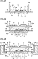
- FIG. 2 is a schematic plan view of the interior of the block module 2 of this embodiment.
- FIG. 3 is a schematic cross-sectional view taken along the line III-III in FIG. 2 .
- FIG. 4 illustrates an example circuit configuration of the block module 2 according to this embodiment.
- the internal structure and circuit configuration of the block module 2 should not be limited to the structure and configuration described in this embodiment.
- the power semiconductor elements 11 are placed on the lead frame 10 encapsulated with the resin material 15.
- the power semiconductor elements 11 each include, for example, an IGBT 11a and a diode 11b.
- the IGBT 11a and the diode 11b are placed in parallel on the lead frame 10.
- the power semiconductor elements 11 are joined to the lead frame 10 with a joining material (not shown).
- a metallic material having excellent thermal conductivity such as Sn-Ag-Cu solder or sinterable Ag paste, is preferably used as the joining material.
- An aluminum (Al) wire having a diameter of about 150 ⁇ m, for example, can be used as the Al wire 14.
- the Al wire 14 does not need to be a wire, and may be a foil-like aluminum (Al) ribbon.
- a thermosetting epoxy resin for transfer molding can be used as the resin material 15.
- the first heatsink 17 is placed on the lower surface of the lead frame 10 with the insulating layer 16 interposed therebetween. Heat generated from the power semiconductor elements 11 is dissipated outwardly through the first heatsink 17.
- a circuit including the power semiconductor elements 11 generates a maximum voltage from several hundred volts to volts higher than 1000 V.
- the first heatsink 17 and the lead frame 10 need to be electrically insulated from each other.
- the insulating layer 16 is provided between the first heatsink 17 and the lead frame 10.
- a resin material having both a heat-dissipation property and an insulation property is preferably used as the insulating layer 16.
- the insulating layer 16 can include a filler having high thermal conductivity, such as alumina or boron nitride.
- the semiconductor device includes, for example, two power semiconductor elements 11 connected in series, and is a single-phase inverter including a positive electrode terminal, a negative electrode terminal, and an AC terminal.
- the two power semiconductor elements 11 are placed on the lead frame 10, one of the power semiconductor elements 11 forms a positive electrode side circuit, and the other one thereof forms a negative electrode side circuit.
- the semiconductor device further includes gates each for switching a corresponding one of the circuits between on and off states.
- a combination of three block modules 2 each having such a circuit configuration enables the formation of a three-phase alternating-current inverter circuit.
- the formation of the three-phase alternating-current inverter circuit enables the formation of a circuit that controls rotation of a motor.
- power semiconductor elements 11 are placed on a prepared lead frame 10.
- IGBTs 11a and diodes 11b are placed on the lead frame 10, and each power semiconductor element 11 includes one of the IGBTs 11a and one of the diodes 11b.
- copper (Cu) having high thermal conductivity is preferably used as the material of the lead frame 10.
- a material having good thermal conductivity is preferably used as a material used to join the power semiconductor elements 11 to the lead frame 10.
- each IGBT 11a and a corresponding one of the diodes 11b are connected in inverse parallel, and the Al wire 14 is connected to the lead frame 10.
- ultrasonic joining is used to join the Al wire 14 to the lead frame 10 to join the Al wire 14 to the lead frame 10.
- the Al wire 14 is preferably joined to the lead frame 10 by ultrasonic joining.
- a first heatsink 17 is adhered to a lower surface of the lead frame 10 with an insulating layer 16 interposed therebetween.
- the insulating layer 16 including an adhesive layer is previously adhered to the first heatsink 17, is formed into a desired shape, and is then adhered to the lead frame 10.
- conditions, such as a temperature need to be adjusted to prevent a loss of adhesiveness of the resin material arising from full curing of the resin material in an initial adhesion step because target objects to be adhered to the insulating layer 16 in this embodiment include two types of objects, i.e., the first heatsink 17 and the lead frame 10.
- a region of the lead frame 10 including the two power semiconductor elements 11 is encapsulated with a resin material 15 to fabricate a block module 2.
- examples of an encapsulation process include a transfer molding process in which a thermosetting epoxy resin serving as the resin material 15 is injected into an encapsulation die (not shown).
- the bottom surface of the first heatsink 17 is designed to contact the encapsulation die, and after encapsulation, the bottom surface of the first heatsink 17 is preferably exposed. The reason for this is that if the resin material 15 flows to the bottom surface of the first heatsink 17 during encapsulation to cover the bottom surface, a path through which heat is dissipated from the power semiconductor elements 11 is blocked to increase the thermal resistance.
- an unnecessary portion of the lead frame 10 is cut away, and a plurality of control terminals 5 are then preferably bent in a direction perpendicular to main circuit terminals 4.
- a block module 2 is first formed by performing this bending process. Each control terminal 5 of the formed block module 2 has already been formed with a protrusion 7.
- the formed block module 2 is placed in an outer case 1.
- the bottom surface of the outer case 1 is inclined at the inclination angle ⁇ described above.
- a feature of the present disclosure is that the bottom surface of the outer case 1 is inclined upwardly toward the interior of the outer case 1 at the inclination angle ⁇ .
- the bottom surface of the outer case 1 inclined at the inclination angle ⁇ provides advantages described below.
- a plurality of block modules 2 can be placed in the outer case 1 along a lateral direction (along the Y axis in FIG. 1 ), and the number of the block modules 2 placed is determined by the circuit configuration of the semiconductor device.
- the outer case 1 needs to include outer case terminals 1a each previously formed at a location corresponding to one of the main circuit terminals 4 of the block modules 2.
- soldering, screwing, caulking, or ultrasonic joining can be used to join each main circuit terminal 4 and a corresponding one of the outer case terminals 1a together.
- a joining material when a joining material is used for soldering or any other process, the difference in coefficient of thermal expansion between the joining material and the main circuit terminal 4 or the outer case terminal 1a may cause a break in the joining material.
- Mechanical fastening such as screwing, increases the contact resistance between a screw and the main circuit terminal 4 or the outer case terminal 1a, and when a large current is passed through the semiconductor device, the resistance may cause a problem.
- a process through which the terminals can be directly joined together such as caulking or ultrasonic joining, is preferably selected to join the terminals.
- caulking is selected, and the main circuit terminal 4 and the outer case terminal 1a are caulked with a caulking tool to form a caulked portion 21, thereby joining the main circuit terminal 4 and the outer case terminal 1a together.
- the control terminals 5 of the block module 2 are inserted through through-holes of the control substrate 3 to electrically join the control substrate 3 and the block module 2 together.
- the control substrate 3 since the control substrate 3 is supported by the protrusions 7 of the control terminals 5, the control substrate 3 can be fixed while the location of the control substrate 3 relative to the block module 2 is regulated.
- the semiconductor device according to this embodiment has a structure that regulates the location of the control substrate 3 as described above. This can reduce the heat transfer from the power semiconductor elements 11 to the control substrate 3, and can prevent the control substrate 3 and a control element 8 from being deteriorated or broken even when the temperature of each power semiconductor element 11 is high.
- a distal end portion of each control terminal 5 is tapered, the control terminal 5 is easily inserted through a corresponding one of the through-holes of the control substrate 3.
- Through-holes or cutouts may be formed in a peripheral portion of the control substrate 3, and a caulking tool may be inserted through each through-hole or each cutout to form a caulked portion 21.
- the outer case 1 is fixed to a second heatsink 25 while being inclined, and the control substrate 3 may be, therefore, warped by being caught in the outer case 1.
- the size of the control substrate 3 is preferably reduced such that the control substrate 3 is located inwardly from the locations at which the main circuit terminals 4 are caulked without forming through-holes or cutouts.
- the semiconductor device according to this embodiment is fabricated through the process steps described above.
- the semiconductor device includes the outer case 1 having two opposite sides each having a bottom surface inclined at the inclination angle ⁇ .
- the outer case 1 when the outer case 1 is fixed on the second heatsink 25 by a plurality of connection screws 60, opposite side surfaces of the outer case 1 are inclined inwardly at the inclination angle ⁇ .
- the outer case 1 inclined at the inclination angle ⁇ is fixed, the outer case 1 is inclined inwardly to allow the first heatsink 17 of the block module 2 to be in close contact with the second heatsink 25.
- the first through holes 20 of the outer case 1 are parallel to the side surfaces of the outer case 1, and the connection screws 60 are each inserted through a corresponding one of the first through holes 20 so as to be inclined at the inclination angle ⁇ relative to the normal to an upper surface of the second heatsink 25.
- the bottom surface of the outer case 1 inclined at the inclination angle ⁇ allows the side surfaces of the outer case 1, which are illustrated in FIG. 1 , to be perpendicular to the bottom surface of the block module 2 before the fixing of the outer case 1 on the second heatsink 25.
- the side surfaces of the outer case 1 fixed on the second heatsink 25 as illustrated in FIG. 7A are inclined at the inclination angle ⁇ relative to the bottom surface of the block module 2, i.e., the top surface of the second heatsink 25.
- the close contact between the block module 2 and the second heatsink 25 can increase heat dissipation from the block module 2 through the first heatsink 17 of the block module 2.
- the close contact corresponds to an example condition of contact.
- the semiconductor device according to this embodiment does not require a metal plate covering the entire bottom surface of the semiconductor device. This prevents variations in thickness of grease due to a warp in a metal plate. Furthermore, the semiconductor device according to this embodiment includes the first heatsink 17 placed in an lower portion of the block module 2, resulting in a reduction in the amount of the block module 2 itself warped. This can reduce the amount of increase in thermal resistance and variations in thermal resistance.
- the inclination angle ⁇ which is illustrated in FIG. 1 and at which the bottom surface of the outer case 1 is inclined from the X plane toward a central portion of the block module 2 is preferably greater than or equal to 0.1° and equal to or less than 10° (0.1 ⁇ ⁇ ⁇ 10°).
- This range corresponds to the range of inclination angles in which fixing the outer case 1 by the connection screws 60 through the first through holes 20 as illustrated in FIG. 7A allows the lead frame 10 to generate an appropriate spring force.
- the inclination angle ⁇ is less than 0.1°, the block module 2 cannot be pressed against the second heatsink 25 in the situation illustrated in FIG. 7A .
- the inclination angle ⁇ is preferably greater than or equal to 0.1°.
- the inclination angle ⁇ is preferably equal to or less than 10°.
- the inclination angle ⁇ of the bottom surface of the outer case 1 is more preferably greater than or equal to 3°.
- the inclination angle ⁇ at which the outer case 1 is inclined toward the central portion of the block module 2 is more preferably greater than or equal to 3° and equal to or less than 10° (3° ⁇ ⁇ 10°).
- the difference D in height between the inner ends of the outer case 1 and the bottom surface of the block module 2 below the inner ends is preferably greater than or equal to 0.05 mm.
- connection screws 60 are used to fix the semiconductor device through the first through holes 20 of the outer case 1 as described above.
- the second heatsink 25 is, for example, an aluminum (Al) heatsink.
- the utilization of the block module can reduce the amount of an encapsulation resin material used when transfer molding is performed using dies.
- Combining the lead frame 10 with the insulating layer 16 enables the replacement of an expensive ceramic substrate with an inexpensive material.
- the structure of the semiconductor device according to this embodiment can sharply reduce the material cost.
- control terminals 5 drawn from the block module 2 are connected to the control substrate 3 immediately above the control terminals 5 (along the Z axis). This can sharply reduce the length of interconnects along lateral directions (along the X axis and the Y axis). This reduction can reduce the inductance of the semiconductor device, thereby reducing electrical damage caused to the semiconductor device by a surge voltage.
- control terminals 5 of the block module 2 may be previously joined to the control substrate 3 as illustrated in FIG. 6C before the block module 2 is placed in the outer case 1.
- the power semiconductor elements 11 are encapsulated with the resin material 15 of the block module 2, and as illustrated in FIG. 1 , an airspace is, therefore, formed between the block module 2 and the control substrate 3.
- the thermal conductivity of the silicone gel 113 for use in the conventional semiconductor device that was described with reference to FIG. 11 is higher than or equal to at least 1 W/(m ⁇ K)
- the thermal conductivity of air is about 0.02-0.03 W/(m ⁇ K).
- the presence of the airspace can significantly reduce the heat transfer to the control substrate 3 as compared with the conventional semiconductor device.
- each power semiconductor element 11 and corresponding ones of the outer case terminals 1a are joined together using the main circuit terminals 4 that are portions of the lead frame 10.
- the pattern of the lead frame 10 can easily increase the junction area (the cross-sectional junction area).
- copper (Cu) having a thermal conductivity of 398 W/(m ⁇ K) is used as the material of the lead frame 10
- heat can be about 1.7 times more easily transferred than when Al having a thermal conductivity of 237 W/(m ⁇ K) is used.
- the properties of Cu also help transfer heat.
- the degree of heat transfer through a current path is much higher than in the conventional semiconductor device, and heat transferred to the control substrate 3 can be, therefore, reduced.
- the control terminals 5 inserted through the through-holes of the control substrate 3 are portions of the lead frame 10 through which heat is more likely to be transferred in terms of the properties of the lead frame 10.
- the cross-sectional area of each control terminal 5 is previously reduced. This reduces heat transferred through the control terminal 5 to the control substrate 3.
- the control terminal 5 transmits only a control signal, and for this reason, even when the cross-sectional area of the control terminal 5 is equal to or less than one half of the cross-sectional area of each main circuit terminal 4, the control terminal 5 is not problematic in terms of electrical characteristics.
- Some of the Al wires 14 connected to the control terminals 5 in the block module 2 are preferably thinner than the other ones of the Al wires 14 joined to the main circuit terminals 4, because heat is less likely to be transferred.
- new power semiconductor elements including a new material, such as silicon carbide (SiC) or gallium nitride (GaN), instead of a conventional material, i.e., silicon (Si), have been becoming commercially practical.
- a new material such as silicon carbide (SiC) or gallium nitride (GaN)
- Si silicon
- Such new power semiconductor elements can operate at a temperature exceeding 150-200° corresponding to conventional operating temperatures, and thus, have been expected to be downsized by simplifying the structures of heat dissipation mechanisms.
- the semiconductor device according to this embodiment is useful, in particular, when used for such a new power semiconductor element requiring heat control measures.
- FIG. 7B illustrates a semiconductor device according to a variation of the first embodiment.
- the semiconductor device includes an outer case 41 including outer case terminals 41a and fixed with an adhesive material.
- the outer case 41 is fixed to a second heatsink 25 with an adhesive instead of by connection screws.
- the semiconductor device according to this variation will be described with reference to FIG. 7B .
- the semiconductor device according to this variation includes an adhesive 23 instead of connection screws 60 as a fixing member for fixing the outer case 41 to the second heatsink 25.
- the adhesive 23 is previously applied to at least the inclined bottom surface of the outer case 41 in which a block module 2 is placed. Thereafter, the outer case 41 placed on a predetermined region of the second heatsink 25 is pressed against the second heatsink 25 by heat to allow a first heatsink 17 exposed from the bottom surface of the block module 2 to be in close contact with an upper surface of the second heatsink 25.
- thermosetting resin for example, can be used as the adhesive 23.
- FIG. 8 is a schematic cross-sectional view of a semiconductor device according to a second embodiment of the present disclosure.
- the semiconductor device according to the second embodiment includes an outer case 51 into which, for example, a block module 52 is incorporated, and a control substrate 53 is placed immediately above the block module 52 (in a positive direction along the Z axis).
- the semiconductor device according to this embodiment can include the outer case 51 into which a plurality of block modules 2 are incorporated.
- the outer case 51 is an example package.
- Main circuit terminals 54 and control terminals 55 are drawn from the block module 52.
- the control terminals 55 each include a protrusion 57, and support the control substrate 53.
- the main circuit terminals 54 extend in lateral directions (along the X axis), and are each electrically connected to a corresponding one of outer case terminals 51a.
- each main circuit terminal 54 is electrically connected to the corresponding one of the outer case terminals 51a by a connection screw 61 inserted through a screw through hole 22 formed in both of the main circuit terminal 54 and the corresponding one of the outer case terminals 51a.
- the connection screw 61 is also a member for fixing the outer case 51 and the block module 52 to a second heatsink 25.
- the control terminals 55 are drawn in a direction perpendicular to the main circuit terminals 54 (in a positive direction along the Z axis), and are inserted through through-holes (not shown) of the control substrate 53. In this case, the control terminals 55 are electrically joined to the control substrate 53 by, for example, soldering.
- the control substrate 53 has a plurality of through holes 53b that are each inclined at an inclination angle ⁇ .
- the through holes 53b are each formed to pass the connection screw 61 therethrough when a corresponding one of the main circuit terminals 54 and a corresponding one of the outer case terminals 51a are screwed.
- the reason why the through holes 53b are inclined at the inclination angle ⁇ is that when the connection screw 61 is passed through a corresponding one of the through holes 53b, the inclination angle ⁇ at which the bottom surface of the outer case 51 is inclined allows the screw through holes 22 to be inclined at the angle ⁇ .
- a peripheral portion of the control substrate 53 can have through holes or cutouts, and the connection screws 61 can be each inserted through a corresponding one of the through holes or a corresponding one of the cutouts to connect a corresponding one of the main circuit terminals 54 to a corresponding one of the outer case terminals 51a. If the control substrate 53 has the through holes or cutouts, the control substrate 53 is fixed to the second heatsink 25 with the outer case 51 inclined. This may cause the control substrate 53 to be caught in the outer case 51, resulting in a warp in the control substrate 53.
- the size of the control substrate 53 is preferably reduced such that the control substrate 53 is located inwardly from portions of the main circuit terminals 54 and portions of the outer case terminals 51a connected using the connection screws 61 without forming through holes or cutouts.
- FIGS. 9A-9C A method for fabricating a semiconductor device according to this embodiment will be described with reference to FIGS. 9A-9C .
- a block module 52 including a plurality of power semiconductor elements 11 is fabricated.
- a control substrate 53 is joined to control terminals 55 of the block module 52.
- an airspace is formed between the control substrate 53 and the block module 52.
- screw through holes 22 of the block module 52 joined to the control substrate 53 are each aligned with a corresponding one of the screw through holes 22 of the outer case 51.
- the outer case 51 and the second heatsink 25 are electrically connected together by connection screws 61, and are fixed.
- the screw through holes 22 of the outer case 51 are parallel to side surfaces of the outer case 51.
- the connection screws 61 are inserted through the screw through holes 22 while being inclined at an inclination angle ⁇ relative to the normal to an upper surface of the second heatsink 25.
- the inclination of the bottom surface of the outer case 51 at the inclination angle ⁇ allows the side surfaces of the outer case 51 illustrated in FIG. 8 to be perpendicular to a lower surface of the block module 52 before the outer case 51 is fixed to the second heatsink 25.
- the side surfaces of the outer case 51 illustrated in FIG. 10 and fixed to the second heatsink 25 are inclined at the inclination angle ⁇ relative to the lower surface of the block module 52, i.e., the upper surface of the second heatsink 25.
- control terminals 55 of the block module 52 may be joined to the control substrate 53 after the block module 52 is placed in the outer case 51.
- a caulking process step can be eliminated, thereby reducing the time period during which process steps are performed.
- the semiconductor devices according to the first and second embodiments are each easily disassembled into the outer case, the block module, and the control substrate by unscrewing the connection screws, and are easily recycled.
- a semiconductor device according to the present disclosure and a method for fabricating the same can be utilized for, for example, power devices used in the form of power conditioners of photovoltaic power generation systems and power devices used to control and the rotation of a motor.
Landscapes
- Engineering & Computer Science (AREA)
- Microelectronics & Electronic Packaging (AREA)
- Physics & Mathematics (AREA)
- Thermal Sciences (AREA)
- Cooling Or The Like Of Semiconductors Or Solid State Devices (AREA)
- Cooling Or The Like Of Electrical Apparatus (AREA)
- Structures Or Materials For Encapsulating Or Coating Semiconductor Devices Or Solid State Devices (AREA)
Claims (13)
- Dispositif à semi-conducteur comprenant:un module de bloc (2, 52) qui comprend intérieurement un élément semi-conducteur de puissance (11) et un premier dissipateur thermique (17) et à partir duquel découlent une borne de circuit principal (4, 54) et une borne de commande (5, 55);un substrat de commande (3, 53) connecté à la borne de commande (5, 55);un boîtier dans lequel sont logés le module de bloc (2, 52) et le substrat de commande (3, 53); etun second dissipateur thermique (25) sur lequel est fixé le boîtier par une vis de connexion (60, 61),dans lequel la vis de connexion (60, 61) est introduite dans le second dissipateur thermique (25) pour être incliné selon un angle d'inclinaison θ par rapport à une normale à une surface du second dissipateur thermique (25),une surface inférieure du boîtier est inclinée par rapport à l'angle d'inclinaison θ par rapport à une surface du second dissipateur thermique (25) dans une situation où le boîtier n'est pas fixé au second dissipateur thermique (25), etlorsque le boîtier n'est pas fixé au second dissipateur thermique (25), une ligne virtuelle (A) connectant les extrémités internes opposées de la surface inclinée du boîtier passe à travers l'intérieur du premier dissipateur thermique (17) du module de bloc (2, 52).
- Dispositif à semi-conducteur selon la revendication 1, dans lequel la vis de connexion (60, 61) permet aux premier et second dissipateurs thermiques (17, 25) d'être en contact étroit l'un avec l'autre.
- Dispositif à semi-conducteur selon les revendications 1 ou 2, dans lequel le boîtier est rectangulaire vu de dessus et
le boîtier est fixé à chacun des deux côtés opposés des quatre côtés du boîtier par la vis de connexion (60, 61). - Dispositif à semi-conducteur selon l'une quelconque des revendications 1 à 3, dans lequel le boîtier est fixé de sorte qu'une surface latérale du boîtier est inclinée selon l'angle d'inclinaison θ par rapport à la normale à la surface du second dissipateur thermique (25).
- Dispositif à semi-conducteur selon l'une quelconque des revendications 1 à 4, dans lequel l'angle d'inclinaison θ est supérieur ou égal à 3° et inférieur ou égal à 10°.
- Dispositif à semi-conducteur selon l'une quelconque des revendications 1 à 5, dans lequel le boîtier est fixé à la second dissipateur thermique (25) par la vis de connexion (60, 61) à travers un trou traversant (53b) formé dans le boîtier.
- Dispositif à semi-conducteur selon l'une quelconque des revendications 1 à 6, dans lequel la borne de circuit principal (4, 54) du module de bloc (2, 52) et une borne de connexion du boîtier sont joints ensemble par calfeutrage.
- Dispositif à semi-conducteur selon l'une quelconque des revendications 1 à 6, dans lequel le boîtier est fixé au second dissipateur thermique (25) par la vis de connexion (60, 61) à travers un trou traversant formé dans la borne de circuit principal et un trou traversant formé dans la borne de connexion du boîtier.
- Dispositif à semi-conducteur comprenant:un module de bloc (2, 52) qui comprend intérieurement un élément semi-conducteur de puissance (11) et un premier dissipateur thermique (17) et à partir duquel découlent une borne de circuit principal (4, 54) et une borne de commande (5, 55);un substrat de commande (3, 53) connecté à la borne de commande (5, 55);un boîtier dans lequel sont logés le module de bloc (2, 52) et le substrat de commande (3, 53); etun second dissipateur thermique (25) sur lequel est fixé le boîtier, dans lequel, lorsque les premier et second dissipateurs thermiques (17, 25) sont disposés en parallèle,une surface inférieure du boîtier est inclinée par rapport à l'angle d'inclinaison θ par rapport à une surface du second dissipateur thermique (25) dans une situation où le boîtier n'est pas fixé au second dissipateur thermique (25), etla surface inférieure du boîtier est parallèle à la surface du second dissipateur thermique (25) dans une situation où le boîtier est fixé sur le second dissipateur thermique (25),lorsque le boîtier n'est pas fixé au second dissipateur thermique (25), une ligne virtuelle (A) connectant les extrémités internes opposées de la surface inclinée du boîtier passe à travers l'intérieur du premier dissipateur thermique (17) du module de bloc (2, 52).
- Procédé de fabrication d'un dispositif à semi-conducteur, le procédé comprenant les étapes suivantes:fabriquer un module de bloc (2, 52) qui comprend intérieurement un élément semi-conducteur de puissance (11) et un premier dissipateur thermique (17) et à partir duquel découlent une borne de circuit principal (4, 54) et une borne de commande (5, 55), un substrat de commande (3, 53) connecté à la borne de commande (5, 55), et un boîtier dans lequel sont logés le module de bloc (2, 52) et le substrat de commande (3, 53), qui comprend une borne de connexion reliée à la borne de circuit principal (4, 54); etfixer le boîtier ayant comme surface inférieure une surface inclinée selon un angle d'inclinaison θ sur un second dissipateur thermique (25) par une vis de connexion (60, 61) introduite dans le second dissipateur thermique (25) selon l'angle d'inclinaison θ par rapport à une normale à une surface du second dissipateur thermique (25),dans lequel, avant de fixer le boîtier au second dissipateur thermique (25), une ligne virtuelle (A) connectant les extrémités internes opposées de la surface inclinée du boîtier passe à travers l'intérieur du premier dissipateur thermique (17) du module de bloc (2, 52).
- Procédé selon la revendication 10, où
le boîtier est rectangulaire vu de dessus, et
le boîtier est fixé à chacun des deux côtés opposés des quatre côtés du boîtier par la vis de connexion (60, 61). - Procédé selon les revendications 10 ou 11, dans lequel l'angle d'inclinaison θ est supérieur ou égal à 3° et inférieur ou égal à 10°.
- Procédé selon l'une quelconque des revendications 10 à 12, dans lequel le boîtier est fixé au second dissipateur thermique (25) par la vis de connexion (60, 61) à travers un trou traversant formé dans la borne de circuit principal et un trou traversant formé dans la borne de connexion du boîtier.
Applications Claiming Priority (2)
| Application Number | Priority Date | Filing Date | Title |
|---|---|---|---|
| JP2012116187 | 2012-05-22 | ||
| PCT/JP2013/002866 WO2013175714A1 (fr) | 2012-05-22 | 2013-04-26 | Dispositif à semi-conducteurs et son procédé de fabrication |
Publications (3)
| Publication Number | Publication Date |
|---|---|
| EP2854174A1 EP2854174A1 (fr) | 2015-04-01 |
| EP2854174A4 EP2854174A4 (fr) | 2015-08-05 |
| EP2854174B1 true EP2854174B1 (fr) | 2019-02-20 |
Family
ID=49623429
Family Applications (1)
| Application Number | Title | Priority Date | Filing Date |
|---|---|---|---|
| EP13793424.6A Active EP2854174B1 (fr) | 2012-05-22 | 2013-04-26 | Dispositif à semi-conducteurs et son procédé de fabrication |
Country Status (5)
| Country | Link |
|---|---|
| US (1) | US9572291B2 (fr) |
| EP (1) | EP2854174B1 (fr) |
| JP (1) | JP5948668B2 (fr) |
| CN (1) | CN104285294B (fr) |
| WO (1) | WO2013175714A1 (fr) |
Families Citing this family (25)
| Publication number | Priority date | Publication date | Assignee | Title |
|---|---|---|---|---|
| JP5542765B2 (ja) * | 2011-09-26 | 2014-07-09 | 日立オートモティブシステムズ株式会社 | パワーモジュール |
| EP2814056B1 (fr) * | 2012-09-13 | 2017-07-12 | Fuji Electric Co., Ltd. | Dispositif à semi-conducteur, procédé destiné à fixer un élément de dissipation de la chaleur sur un dispositif à semi-conducteur, et procédé destiné à fabriquer un dispositif à semi-conducteur |
| JP6459418B2 (ja) * | 2014-11-13 | 2019-01-30 | 富士電機株式会社 | 半導体装置およびその製造方法 |
| CN106298688B (zh) * | 2015-05-28 | 2018-11-06 | 台达电子工业股份有限公司 | 封装型功率电路模块 |
| JP6455364B2 (ja) | 2015-08-28 | 2019-01-23 | 三菱電機株式会社 | 半導体装置、インテリジェントパワーモジュールおよび電力変換装置 |
| WO2017040787A1 (fr) * | 2015-09-01 | 2017-03-09 | Macom Technology Solutions Holdings, Inc. | Conditionnement à cavités d'air |
| ITUB20153344A1 (it) * | 2015-09-02 | 2017-03-02 | St Microelectronics Srl | Modulo di potenza elettronico con migliorata dissipazione termica e relativo metodo di fabbricazione |
| JP6631114B2 (ja) * | 2015-09-17 | 2020-01-15 | 富士電機株式会社 | 半導体装置及び半導体装置の計測方法 |
| JP6759784B2 (ja) * | 2016-07-12 | 2020-09-23 | 三菱電機株式会社 | 半導体モジュール |
| DE112016007133B4 (de) * | 2016-08-10 | 2021-08-12 | Mitsubishi Electric Corporation | Halbleitervorrichtung |
| JP6395164B1 (ja) * | 2017-04-20 | 2018-09-26 | 三菱電機株式会社 | 電力変換装置 |
| JP6769556B2 (ja) * | 2017-07-28 | 2020-10-14 | 三菱電機株式会社 | 半導体装置及び半導体モジュール |
| CA3075179C (fr) * | 2017-09-07 | 2025-05-20 | Green Cubes Technology, Llc | Systèmes électriques et procédés d’utilisation de ces derniers pour fournir de l’énergie |
| CN109906509B (zh) * | 2017-10-10 | 2022-10-28 | 新电元工业株式会社 | 模块以及电力转换装置 |
| EP3499563B1 (fr) * | 2017-12-13 | 2020-04-15 | SEMIKRON Elektronik GmbH & Co. KG | Module semi-conducteur de puissance et procédé de positionnement en force d'un module semi-conducteur de puissance |
| US10784183B2 (en) * | 2018-11-30 | 2020-09-22 | Infineon Technologies Ag | Semiconductor module with package extension frames |
| US11715679B2 (en) * | 2019-10-09 | 2023-08-01 | Texas Instruments Incorporated | Power stage package including flexible circuit and stacked die |
| US11264311B2 (en) * | 2019-10-11 | 2022-03-01 | Semiconductor Components Industries, Llc | Clips for semiconductor package and related methods |
| JP6928129B2 (ja) * | 2020-01-17 | 2021-09-01 | 三菱電機株式会社 | 電力変換装置 |
| JP7286582B2 (ja) | 2020-03-24 | 2023-06-05 | 株式会社東芝 | 半導体装置 |
| EP3936722B1 (fr) * | 2020-07-06 | 2024-09-04 | Schott Ag | Partie de boîtier, en particulier une partie de boîtier d'un boîtier électronique, de préférence un terminal de compresseur électronique |
| JP7528634B2 (ja) * | 2020-08-25 | 2024-08-06 | 富士電機株式会社 | 半導体装置及び半導体装置の製造方法 |
| US20220396154A1 (en) * | 2021-06-14 | 2022-12-15 | Panasonic Intellectual Property Management Co., Ltd. | Vehicle mounted electric power converter |
| JP7378096B2 (ja) * | 2021-12-23 | 2023-11-13 | 三安ジャパンテクノロジー株式会社 | モジュールおよびモジュールの製造方法 |
| JP2024106060A (ja) * | 2023-01-26 | 2024-08-07 | 三菱電機株式会社 | 半導体装置 |
Family Cites Families (30)
| Publication number | Priority date | Publication date | Assignee | Title |
|---|---|---|---|---|
| JPH04233752A (ja) | 1990-12-28 | 1992-08-21 | Shinko Electric Ind Co Ltd | 電子部品用パッケージ |
| JP3110657B2 (ja) * | 1995-08-02 | 2000-11-20 | 松下電子工業株式会社 | 樹脂封止型半導体装置およびその製造方法 |
| US6147869A (en) * | 1997-11-24 | 2000-11-14 | International Rectifier Corp. | Adaptable planar module |
| JP3674333B2 (ja) * | 1998-09-11 | 2005-07-20 | 株式会社日立製作所 | パワー半導体モジュール並びにそれを用いた電動機駆動システム |
| JP4054137B2 (ja) * | 1999-06-03 | 2008-02-27 | 株式会社東京アールアンドデー | パワー半導体素子の給電及び放熱装置 |
| JP4027558B2 (ja) * | 2000-03-03 | 2007-12-26 | 三菱電機株式会社 | パワーモジュール |
| JP4218193B2 (ja) * | 2000-08-24 | 2009-02-04 | 三菱電機株式会社 | パワーモジュール |
| US7061080B2 (en) * | 2001-06-11 | 2006-06-13 | Fairchild Korea Semiconductor Ltd. | Power module package having improved heat dissipating capability |
| US6974460B2 (en) * | 2001-09-14 | 2005-12-13 | Stryker Spine | Biased angulation bone fixation assembly |
| JP4177571B2 (ja) * | 2001-09-20 | 2008-11-05 | 三菱電機株式会社 | 半導体装置 |
| JP3813098B2 (ja) * | 2002-02-14 | 2006-08-23 | 三菱電機株式会社 | 電力用半導体モジュール |
| JP3764687B2 (ja) * | 2002-02-18 | 2006-04-12 | 三菱電機株式会社 | 電力半導体装置及びその製造方法 |
| JP3828036B2 (ja) * | 2002-03-28 | 2006-09-27 | 三菱電機株式会社 | 樹脂モールド型デバイスの製造方法及び製造装置 |
| JP3740116B2 (ja) * | 2002-11-11 | 2006-02-01 | 三菱電機株式会社 | モールド樹脂封止型パワー半導体装置及びその製造方法 |
| WO2004093187A1 (fr) * | 2003-04-16 | 2004-10-28 | Fujitsu Limited | Boitier pour composants electroniques, ensemble boitier pour composants electroniques et unite de circuit imprime |
| JP4391407B2 (ja) * | 2004-12-20 | 2009-12-24 | 三菱電機株式会社 | 制御装置一体型回転電機 |
| US7766943B1 (en) * | 2005-08-11 | 2010-08-03 | Medicine Lodge Inc. | Modular percutaneous spinal fusion system and method |
| CN200990577Y (zh) * | 2006-08-28 | 2007-12-12 | 中山大洋电机股份有限公司 | 一种直流无刷电机的控制器结构 |
| EP1914470B1 (fr) * | 2006-10-20 | 2016-05-18 | OSRAM GmbH | Lampe à semi-conducteur |
| TWI402952B (zh) * | 2007-09-27 | 2013-07-21 | 三洋電機股份有限公司 | 電路裝置及其製造方法 |
| JP4934559B2 (ja) * | 2007-09-27 | 2012-05-16 | オンセミコンダクター・トレーディング・リミテッド | 回路装置およびその製造方法 |
| JP2009099339A (ja) | 2007-10-16 | 2009-05-07 | Mitsubishi Electric Corp | 電子機器の配線接続構造及び方法 |
| EP2154419B1 (fr) * | 2008-07-31 | 2016-07-06 | Toshiba Lighting & Technology Corporation | Lampe à lumière mixte |
| JP5435286B2 (ja) * | 2009-06-24 | 2014-03-05 | 株式会社デンソー | 駆動装置 |
| JP5177711B2 (ja) * | 2010-05-21 | 2013-04-10 | 株式会社デンソー | 電動装置 |
| JP5692575B2 (ja) * | 2010-12-28 | 2015-04-01 | 株式会社デンソー | 駆動装置 |
| JP5351907B2 (ja) * | 2011-01-13 | 2013-11-27 | アイシン・エィ・ダブリュ株式会社 | 半導体装置 |
| US20120250335A1 (en) * | 2011-03-08 | 2012-10-04 | Panasonic Corporation | Illumination apparatus and fan unit for illumination apparatus |
| US8304871B2 (en) * | 2011-04-05 | 2012-11-06 | Texas Instruments Incorporated | Exposed die package for direct surface mounting |
| JP5692593B2 (ja) * | 2011-05-11 | 2015-04-01 | 株式会社デンソー | 駆動装置 |
-
2013
- 2013-04-26 EP EP13793424.6A patent/EP2854174B1/fr active Active
- 2013-04-26 WO PCT/JP2013/002866 patent/WO2013175714A1/fr not_active Ceased
- 2013-04-26 CN CN201380024660.7A patent/CN104285294B/zh active Active
- 2013-04-26 JP JP2014516649A patent/JP5948668B2/ja active Active
- 2013-04-26 US US14/395,411 patent/US9572291B2/en active Active
Non-Patent Citations (1)
| Title |
|---|
| None * |
Also Published As
| Publication number | Publication date |
|---|---|
| US20150116945A1 (en) | 2015-04-30 |
| CN104285294B (zh) | 2016-11-09 |
| JP5948668B2 (ja) | 2016-07-06 |
| US9572291B2 (en) | 2017-02-14 |
| CN104285294A (zh) | 2015-01-14 |
| WO2013175714A1 (fr) | 2013-11-28 |
| JPWO2013175714A1 (ja) | 2016-01-12 |
| EP2854174A4 (fr) | 2015-08-05 |
| EP2854174A1 (fr) | 2015-04-01 |
Similar Documents
| Publication | Publication Date | Title |
|---|---|---|
| EP2854174B1 (fr) | Dispositif à semi-conducteurs et son procédé de fabrication | |
| US10861833B2 (en) | Semiconductor device | |
| US9171773B2 (en) | Semiconductor device | |
| US8324726B2 (en) | Semiconductor device, electrode member and electrode member fabrication method | |
| US9754855B2 (en) | Semiconductor module having an embedded metal heat dissipation plate | |
| US8610263B2 (en) | Semiconductor device module | |
| US10163752B2 (en) | Semiconductor device | |
| CN105874596A (zh) | 半导体模块 | |
| EP4148778B1 (fr) | Module semi-conducteur de puissance | |
| US9437508B2 (en) | Method for manufacturing semiconductor device and semiconductor device | |
| JP6061967B2 (ja) | パワー半導体装置 | |
| CN117438386A (zh) | 半导体装置、半导体装置的制造方法及电力转换装置 | |
| CN114446916A (zh) | 三层级互连夹 | |
| CN104798194B (zh) | 半导体器件 | |
| EP3410481A1 (fr) | Module de puce d'alimentation à semi-conducteur | |
| EP2680305A2 (fr) | Boîtier de semi-conducteur | |
| US9099451B2 (en) | Power module package and method of manufacturing the same | |
| JP2013157485A (ja) | 半導体装置とその製造方法 | |
| US20250218887A1 (en) | Semiconductor device and manufacturing method of semiconductor device | |
| JP2025115059A (ja) | 半導体モジュール | |
| CN116403997A (zh) | 半导体装置 |
Legal Events
| Date | Code | Title | Description |
|---|---|---|---|
| PUAI | Public reference made under article 153(3) epc to a published international application that has entered the european phase |
Free format text: ORIGINAL CODE: 0009012 |
|
| 17P | Request for examination filed |
Effective date: 20141105 |
|
| AK | Designated contracting states |
Kind code of ref document: A1 Designated state(s): AL AT BE BG CH CY CZ DE DK EE ES FI FR GB GR HR HU IE IS IT LI LT LU LV MC MK MT NL NO PL PT RO RS SE SI SK SM TR |
|
| AX | Request for extension of the european patent |
Extension state: BA ME |
|
| RA4 | Supplementary search report drawn up and despatched (corrected) |
Effective date: 20150703 |
|
| RIC1 | Information provided on ipc code assigned before grant |
Ipc: H01L 23/40 20060101AFI20150629BHEP Ipc: H01L 25/16 20060101ALI20150629BHEP Ipc: H01L 23/495 20060101ALI20150629BHEP |
|
| DAX | Request for extension of the european patent (deleted) | ||
| STAA | Information on the status of an ep patent application or granted ep patent |
Free format text: STATUS: EXAMINATION IS IN PROGRESS |
|
| 17Q | First examination report despatched |
Effective date: 20180110 |
|
| GRAP | Despatch of communication of intention to grant a patent |
Free format text: ORIGINAL CODE: EPIDOSNIGR1 |
|
| STAA | Information on the status of an ep patent application or granted ep patent |
Free format text: STATUS: GRANT OF PATENT IS INTENDED |
|
| INTG | Intention to grant announced |
Effective date: 20180905 |
|
| GRAS | Grant fee paid |
Free format text: ORIGINAL CODE: EPIDOSNIGR3 |
|
| GRAA | (expected) grant |
Free format text: ORIGINAL CODE: 0009210 |
|
| STAA | Information on the status of an ep patent application or granted ep patent |
Free format text: STATUS: THE PATENT HAS BEEN GRANTED |
|
| AK | Designated contracting states |
Kind code of ref document: B1 Designated state(s): AL AT BE BG CH CY CZ DE DK EE ES FI FR GB GR HR HU IE IS IT LI LT LU LV MC MK MT NL NO PL PT RO RS SE SI SK SM TR |
|
| REG | Reference to a national code |
Ref country code: GB Ref legal event code: FG4D |
|
| REG | Reference to a national code |
Ref country code: CH Ref legal event code: EP |
|
| REG | Reference to a national code |
Ref country code: DE Ref legal event code: R096 Ref document number: 602013051040 Country of ref document: DE |
|
| REG | Reference to a national code |
Ref country code: AT Ref legal event code: REF Ref document number: 1099297 Country of ref document: AT Kind code of ref document: T Effective date: 20190315 |
|
| REG | Reference to a national code |
Ref country code: IE Ref legal event code: FG4D |
|
| REG | Reference to a national code |
Ref country code: NL Ref legal event code: MP Effective date: 20190220 |
|
| REG | Reference to a national code |
Ref country code: LT Ref legal event code: MG4D |
|
| PG25 | Lapsed in a contracting state [announced via postgrant information from national office to epo] |
Ref country code: PT Free format text: LAPSE BECAUSE OF FAILURE TO SUBMIT A TRANSLATION OF THE DESCRIPTION OR TO PAY THE FEE WITHIN THE PRESCRIBED TIME-LIMIT Effective date: 20190620 Ref country code: SE Free format text: LAPSE BECAUSE OF FAILURE TO SUBMIT A TRANSLATION OF THE DESCRIPTION OR TO PAY THE FEE WITHIN THE PRESCRIBED TIME-LIMIT Effective date: 20190220 Ref country code: NO Free format text: LAPSE BECAUSE OF FAILURE TO SUBMIT A TRANSLATION OF THE DESCRIPTION OR TO PAY THE FEE WITHIN THE PRESCRIBED TIME-LIMIT Effective date: 20190520 Ref country code: FI Free format text: LAPSE BECAUSE OF FAILURE TO SUBMIT A TRANSLATION OF THE DESCRIPTION OR TO PAY THE FEE WITHIN THE PRESCRIBED TIME-LIMIT Effective date: 20190220 Ref country code: LT Free format text: LAPSE BECAUSE OF FAILURE TO SUBMIT A TRANSLATION OF THE DESCRIPTION OR TO PAY THE FEE WITHIN THE PRESCRIBED TIME-LIMIT Effective date: 20190220 Ref country code: NL Free format text: LAPSE BECAUSE OF FAILURE TO SUBMIT A TRANSLATION OF THE DESCRIPTION OR TO PAY THE FEE WITHIN THE PRESCRIBED TIME-LIMIT Effective date: 20190220 |
|
| PG25 | Lapsed in a contracting state [announced via postgrant information from national office to epo] |
Ref country code: GR Free format text: LAPSE BECAUSE OF FAILURE TO SUBMIT A TRANSLATION OF THE DESCRIPTION OR TO PAY THE FEE WITHIN THE PRESCRIBED TIME-LIMIT Effective date: 20190521 Ref country code: BG Free format text: LAPSE BECAUSE OF FAILURE TO SUBMIT A TRANSLATION OF THE DESCRIPTION OR TO PAY THE FEE WITHIN THE PRESCRIBED TIME-LIMIT Effective date: 20190520 Ref country code: RS Free format text: LAPSE BECAUSE OF FAILURE TO SUBMIT A TRANSLATION OF THE DESCRIPTION OR TO PAY THE FEE WITHIN THE PRESCRIBED TIME-LIMIT Effective date: 20190220 Ref country code: HR Free format text: LAPSE BECAUSE OF FAILURE TO SUBMIT A TRANSLATION OF THE DESCRIPTION OR TO PAY THE FEE WITHIN THE PRESCRIBED TIME-LIMIT Effective date: 20190220 Ref country code: LV Free format text: LAPSE BECAUSE OF FAILURE TO SUBMIT A TRANSLATION OF THE DESCRIPTION OR TO PAY THE FEE WITHIN THE PRESCRIBED TIME-LIMIT Effective date: 20190220 Ref country code: IS Free format text: LAPSE BECAUSE OF FAILURE TO SUBMIT A TRANSLATION OF THE DESCRIPTION OR TO PAY THE FEE WITHIN THE PRESCRIBED TIME-LIMIT Effective date: 20190620 |
|
| REG | Reference to a national code |
Ref country code: AT Ref legal event code: MK05 Ref document number: 1099297 Country of ref document: AT Kind code of ref document: T Effective date: 20190220 |
|
| PG25 | Lapsed in a contracting state [announced via postgrant information from national office to epo] |
Ref country code: RO Free format text: LAPSE BECAUSE OF FAILURE TO SUBMIT A TRANSLATION OF THE DESCRIPTION OR TO PAY THE FEE WITHIN THE PRESCRIBED TIME-LIMIT Effective date: 20190220 Ref country code: IT Free format text: LAPSE BECAUSE OF FAILURE TO SUBMIT A TRANSLATION OF THE DESCRIPTION OR TO PAY THE FEE WITHIN THE PRESCRIBED TIME-LIMIT Effective date: 20190220 Ref country code: CZ Free format text: LAPSE BECAUSE OF FAILURE TO SUBMIT A TRANSLATION OF THE DESCRIPTION OR TO PAY THE FEE WITHIN THE PRESCRIBED TIME-LIMIT Effective date: 20190220 Ref country code: SK Free format text: LAPSE BECAUSE OF FAILURE TO SUBMIT A TRANSLATION OF THE DESCRIPTION OR TO PAY THE FEE WITHIN THE PRESCRIBED TIME-LIMIT Effective date: 20190220 Ref country code: AL Free format text: LAPSE BECAUSE OF FAILURE TO SUBMIT A TRANSLATION OF THE DESCRIPTION OR TO PAY THE FEE WITHIN THE PRESCRIBED TIME-LIMIT Effective date: 20190220 Ref country code: EE Free format text: LAPSE BECAUSE OF FAILURE TO SUBMIT A TRANSLATION OF THE DESCRIPTION OR TO PAY THE FEE WITHIN THE PRESCRIBED TIME-LIMIT Effective date: 20190220 Ref country code: DK Free format text: LAPSE BECAUSE OF FAILURE TO SUBMIT A TRANSLATION OF THE DESCRIPTION OR TO PAY THE FEE WITHIN THE PRESCRIBED TIME-LIMIT Effective date: 20190220 Ref country code: ES Free format text: LAPSE BECAUSE OF FAILURE TO SUBMIT A TRANSLATION OF THE DESCRIPTION OR TO PAY THE FEE WITHIN THE PRESCRIBED TIME-LIMIT Effective date: 20190220 |
|
| REG | Reference to a national code |
Ref country code: DE Ref legal event code: R097 Ref document number: 602013051040 Country of ref document: DE |
|
| PG25 | Lapsed in a contracting state [announced via postgrant information from national office to epo] |
Ref country code: SM Free format text: LAPSE BECAUSE OF FAILURE TO SUBMIT A TRANSLATION OF THE DESCRIPTION OR TO PAY THE FEE WITHIN THE PRESCRIBED TIME-LIMIT Effective date: 20190220 Ref country code: PL Free format text: LAPSE BECAUSE OF FAILURE TO SUBMIT A TRANSLATION OF THE DESCRIPTION OR TO PAY THE FEE WITHIN THE PRESCRIBED TIME-LIMIT Effective date: 20190220 |
|
| REG | Reference to a national code |
Ref country code: CH Ref legal event code: PL |
|
| REG | Reference to a national code |
Ref country code: BE Ref legal event code: MM Effective date: 20190430 |
|
| PLBE | No opposition filed within time limit |
Free format text: ORIGINAL CODE: 0009261 |
|
| STAA | Information on the status of an ep patent application or granted ep patent |
Free format text: STATUS: NO OPPOSITION FILED WITHIN TIME LIMIT |
|
| PG25 | Lapsed in a contracting state [announced via postgrant information from national office to epo] |
Ref country code: LU Free format text: LAPSE BECAUSE OF NON-PAYMENT OF DUE FEES Effective date: 20190426 Ref country code: AT Free format text: LAPSE BECAUSE OF FAILURE TO SUBMIT A TRANSLATION OF THE DESCRIPTION OR TO PAY THE FEE WITHIN THE PRESCRIBED TIME-LIMIT Effective date: 20190220 Ref country code: MC Free format text: LAPSE BECAUSE OF FAILURE TO SUBMIT A TRANSLATION OF THE DESCRIPTION OR TO PAY THE FEE WITHIN THE PRESCRIBED TIME-LIMIT Effective date: 20190220 |
|
| 26N | No opposition filed |
Effective date: 20191121 |
|
| GBPC | Gb: european patent ceased through non-payment of renewal fee |
Effective date: 20190520 |
|
| PG25 | Lapsed in a contracting state [announced via postgrant information from national office to epo] |
Ref country code: LI Free format text: LAPSE BECAUSE OF NON-PAYMENT OF DUE FEES Effective date: 20190430 Ref country code: CH Free format text: LAPSE BECAUSE OF NON-PAYMENT OF DUE FEES Effective date: 20190430 |
|
| PG25 | Lapsed in a contracting state [announced via postgrant information from national office to epo] |
Ref country code: SI Free format text: LAPSE BECAUSE OF FAILURE TO SUBMIT A TRANSLATION OF THE DESCRIPTION OR TO PAY THE FEE WITHIN THE PRESCRIBED TIME-LIMIT Effective date: 20190220 Ref country code: FR Free format text: LAPSE BECAUSE OF NON-PAYMENT OF DUE FEES Effective date: 20190430 Ref country code: BE Free format text: LAPSE BECAUSE OF NON-PAYMENT OF DUE FEES Effective date: 20190430 |
|
| PG25 | Lapsed in a contracting state [announced via postgrant information from national office to epo] |
Ref country code: TR Free format text: LAPSE BECAUSE OF FAILURE TO SUBMIT A TRANSLATION OF THE DESCRIPTION OR TO PAY THE FEE WITHIN THE PRESCRIBED TIME-LIMIT Effective date: 20190220 |
|
| PG25 | Lapsed in a contracting state [announced via postgrant information from national office to epo] |
Ref country code: GB Free format text: LAPSE BECAUSE OF NON-PAYMENT OF DUE FEES Effective date: 20190520 Ref country code: IE Free format text: LAPSE BECAUSE OF NON-PAYMENT OF DUE FEES Effective date: 20190426 |
|
| PG25 | Lapsed in a contracting state [announced via postgrant information from national office to epo] |
Ref country code: CY Free format text: LAPSE BECAUSE OF FAILURE TO SUBMIT A TRANSLATION OF THE DESCRIPTION OR TO PAY THE FEE WITHIN THE PRESCRIBED TIME-LIMIT Effective date: 20190220 |
|
| PG25 | Lapsed in a contracting state [announced via postgrant information from national office to epo] |
Ref country code: MT Free format text: LAPSE BECAUSE OF FAILURE TO SUBMIT A TRANSLATION OF THE DESCRIPTION OR TO PAY THE FEE WITHIN THE PRESCRIBED TIME-LIMIT Effective date: 20190220 Ref country code: HU Free format text: LAPSE BECAUSE OF FAILURE TO SUBMIT A TRANSLATION OF THE DESCRIPTION OR TO PAY THE FEE WITHIN THE PRESCRIBED TIME-LIMIT; INVALID AB INITIO Effective date: 20130426 |
|
| PG25 | Lapsed in a contracting state [announced via postgrant information from national office to epo] |
Ref country code: MK Free format text: LAPSE BECAUSE OF FAILURE TO SUBMIT A TRANSLATION OF THE DESCRIPTION OR TO PAY THE FEE WITHIN THE PRESCRIBED TIME-LIMIT Effective date: 20190220 |
|
| PGFP | Annual fee paid to national office [announced via postgrant information from national office to epo] |
Ref country code: DE Payment date: 20250422 Year of fee payment: 13 |
|
| REG | Reference to a national code |
Ref country code: DE Ref legal event code: R079 Ref document number: 602013051040 Country of ref document: DE Free format text: PREVIOUS MAIN CLASS: H01L0023400000 Ipc: H10W0040600000 |