EP2863430A2 - Dispositif semi-conducteur - Google Patents
Dispositif semi-conducteur Download PDFInfo
- Publication number
- EP2863430A2 EP2863430A2 EP20150150440 EP15150440A EP2863430A2 EP 2863430 A2 EP2863430 A2 EP 2863430A2 EP 20150150440 EP20150150440 EP 20150150440 EP 15150440 A EP15150440 A EP 15150440A EP 2863430 A2 EP2863430 A2 EP 2863430A2
- Authority
- EP
- European Patent Office
- Prior art keywords
- film
- insulating film
- hole
- groove
- inter
- Prior art date
- Legal status (The legal status is an assumption and is not a legal conclusion. Google has not performed a legal analysis and makes no representation as to the accuracy of the status listed.)
- Granted
Links
Images
















Classifications
-
- H—ELECTRICITY
- H10—SEMICONDUCTOR DEVICES; ELECTRIC SOLID-STATE DEVICES NOT OTHERWISE PROVIDED FOR
- H10W—GENERIC PACKAGES, INTERCONNECTIONS, CONNECTORS OR OTHER CONSTRUCTIONAL DETAILS OF DEVICES COVERED BY CLASS H10
- H10W20/00—Interconnections in chips, wafers or substrates
- H10W20/01—Manufacture or treatment
- H10W20/031—Manufacture or treatment of conductive parts of the interconnections
- H10W20/056—Manufacture or treatment of conductive parts of the interconnections by filling conductive material into holes, grooves or trenches
-
- H—ELECTRICITY
- H10—SEMICONDUCTOR DEVICES; ELECTRIC SOLID-STATE DEVICES NOT OTHERWISE PROVIDED FOR
- H10D—INORGANIC ELECTRIC SEMICONDUCTOR DEVICES
- H10D84/00—Integrated devices formed in or on semiconductor substrates that comprise only semiconducting layers, e.g. on Si wafers or on GaAs-on-Si wafers
-
- H—ELECTRICITY
- H10—SEMICONDUCTOR DEVICES; ELECTRIC SOLID-STATE DEVICES NOT OTHERWISE PROVIDED FOR
- H10D—INORGANIC ELECTRIC SEMICONDUCTOR DEVICES
- H10D62/00—Semiconductor bodies, or regions thereof, of devices having potential barriers
- H10D62/10—Shapes, relative sizes or dispositions of the regions of the semiconductor bodies; Shapes of the semiconductor bodies
- H10D62/102—Constructional design considerations for preventing surface leakage or controlling electric field concentration
-
- H—ELECTRICITY
- H10—SEMICONDUCTOR DEVICES; ELECTRIC SOLID-STATE DEVICES NOT OTHERWISE PROVIDED FOR
- H10D—INORGANIC ELECTRIC SEMICONDUCTOR DEVICES
- H10D62/00—Semiconductor bodies, or regions thereof, of devices having potential barriers
- H10D62/10—Shapes, relative sizes or dispositions of the regions of the semiconductor bodies; Shapes of the semiconductor bodies
- H10D62/102—Constructional design considerations for preventing surface leakage or controlling electric field concentration
- H10D62/103—Constructional design considerations for preventing surface leakage or controlling electric field concentration for increasing or controlling the breakdown voltage of reverse-biased devices
-
- H—ELECTRICITY
- H10—SEMICONDUCTOR DEVICES; ELECTRIC SOLID-STATE DEVICES NOT OTHERWISE PROVIDED FOR
- H10D—INORGANIC ELECTRIC SEMICONDUCTOR DEVICES
- H10D62/00—Semiconductor bodies, or regions thereof, of devices having potential barriers
- H10D62/10—Shapes, relative sizes or dispositions of the regions of the semiconductor bodies; Shapes of the semiconductor bodies
- H10D62/102—Constructional design considerations for preventing surface leakage or controlling electric field concentration
- H10D62/103—Constructional design considerations for preventing surface leakage or controlling electric field concentration for increasing or controlling the breakdown voltage of reverse-biased devices
- H10D62/105—Constructional design considerations for preventing surface leakage or controlling electric field concentration for increasing or controlling the breakdown voltage of reverse-biased devices by having particular doping profiles, shapes or arrangements of PN junctions; by having supplementary regions, e.g. junction termination extension [JTE]
- H10D62/106—Constructional design considerations for preventing surface leakage or controlling electric field concentration for increasing or controlling the breakdown voltage of reverse-biased devices by having particular doping profiles, shapes or arrangements of PN junctions; by having supplementary regions, e.g. junction termination extension [JTE] having supplementary regions doped oppositely to or in rectifying contact with regions of the semiconductor bodies, e.g. guard rings with PN or Schottky junctions
-
- H—ELECTRICITY
- H10—SEMICONDUCTOR DEVICES; ELECTRIC SOLID-STATE DEVICES NOT OTHERWISE PROVIDED FOR
- H10W—GENERIC PACKAGES, INTERCONNECTIONS, CONNECTORS OR OTHER CONSTRUCTIONAL DETAILS OF DEVICES COVERED BY CLASS H10
- H10W20/00—Interconnections in chips, wafers or substrates
- H10W20/01—Manufacture or treatment
- H10W20/031—Manufacture or treatment of conductive parts of the interconnections
- H10W20/032—Manufacture or treatment of conductive parts of the interconnections of conductive barrier, adhesion or liner layers
- H10W20/033—Manufacture or treatment of conductive parts of the interconnections of conductive barrier, adhesion or liner layers in openings in dielectrics
-
- H—ELECTRICITY
- H10—SEMICONDUCTOR DEVICES; ELECTRIC SOLID-STATE DEVICES NOT OTHERWISE PROVIDED FOR
- H10W—GENERIC PACKAGES, INTERCONNECTIONS, CONNECTORS OR OTHER CONSTRUCTIONAL DETAILS OF DEVICES COVERED BY CLASS H10
- H10W20/00—Interconnections in chips, wafers or substrates
- H10W20/01—Manufacture or treatment
- H10W20/071—Manufacture or treatment of dielectric parts thereof
- H10W20/081—Manufacture or treatment of dielectric parts thereof by forming openings in the dielectric parts
- H10W20/082—Manufacture or treatment of dielectric parts thereof by forming openings in the dielectric parts the openings being tapered via holes
-
- H—ELECTRICITY
- H10—SEMICONDUCTOR DEVICES; ELECTRIC SOLID-STATE DEVICES NOT OTHERWISE PROVIDED FOR
- H10W—GENERIC PACKAGES, INTERCONNECTIONS, CONNECTORS OR OTHER CONSTRUCTIONAL DETAILS OF DEVICES COVERED BY CLASS H10
- H10W20/00—Interconnections in chips, wafers or substrates
- H10W20/20—Interconnections within wafers or substrates, e.g. through-silicon vias [TSV]
-
- H—ELECTRICITY
- H10—SEMICONDUCTOR DEVICES; ELECTRIC SOLID-STATE DEVICES NOT OTHERWISE PROVIDED FOR
- H10W—GENERIC PACKAGES, INTERCONNECTIONS, CONNECTORS OR OTHER CONSTRUCTIONAL DETAILS OF DEVICES COVERED BY CLASS H10
- H10W20/00—Interconnections in chips, wafers or substrates
- H10W20/40—Interconnections external to wafers or substrates, e.g. back-end-of-line [BEOL] metallisations or vias connecting to gate electrodes
-
- H—ELECTRICITY
- H10—SEMICONDUCTOR DEVICES; ELECTRIC SOLID-STATE DEVICES NOT OTHERWISE PROVIDED FOR
- H10W—GENERIC PACKAGES, INTERCONNECTIONS, CONNECTORS OR OTHER CONSTRUCTIONAL DETAILS OF DEVICES COVERED BY CLASS H10
- H10W20/00—Interconnections in chips, wafers or substrates
- H10W20/40—Interconnections external to wafers or substrates, e.g. back-end-of-line [BEOL] metallisations or vias connecting to gate electrodes
- H10W20/41—Interconnections external to wafers or substrates, e.g. back-end-of-line [BEOL] metallisations or vias connecting to gate electrodes characterised by their conductive parts
- H10W20/42—Vias, e.g. via plugs
-
- H—ELECTRICITY
- H10—SEMICONDUCTOR DEVICES; ELECTRIC SOLID-STATE DEVICES NOT OTHERWISE PROVIDED FOR
- H10W—GENERIC PACKAGES, INTERCONNECTIONS, CONNECTORS OR OTHER CONSTRUCTIONAL DETAILS OF DEVICES COVERED BY CLASS H10
- H10W20/00—Interconnections in chips, wafers or substrates
- H10W20/40—Interconnections external to wafers or substrates, e.g. back-end-of-line [BEOL] metallisations or vias connecting to gate electrodes
- H10W20/41—Interconnections external to wafers or substrates, e.g. back-end-of-line [BEOL] metallisations or vias connecting to gate electrodes characterised by their conductive parts
- H10W20/425—Barrier, adhesion or liner layers
-
- H—ELECTRICITY
- H10—SEMICONDUCTOR DEVICES; ELECTRIC SOLID-STATE DEVICES NOT OTHERWISE PROVIDED FOR
- H10W—GENERIC PACKAGES, INTERCONNECTIONS, CONNECTORS OR OTHER CONSTRUCTIONAL DETAILS OF DEVICES COVERED BY CLASS H10
- H10W20/00—Interconnections in chips, wafers or substrates
- H10W20/40—Interconnections external to wafers or substrates, e.g. back-end-of-line [BEOL] metallisations or vias connecting to gate electrodes
- H10W20/41—Interconnections external to wafers or substrates, e.g. back-end-of-line [BEOL] metallisations or vias connecting to gate electrodes characterised by their conductive parts
- H10W20/43—Layouts of interconnections
-
- H—ELECTRICITY
- H10—SEMICONDUCTOR DEVICES; ELECTRIC SOLID-STATE DEVICES NOT OTHERWISE PROVIDED FOR
- H10W—GENERIC PACKAGES, INTERCONNECTIONS, CONNECTORS OR OTHER CONSTRUCTIONAL DETAILS OF DEVICES COVERED BY CLASS H10
- H10W20/00—Interconnections in chips, wafers or substrates
- H10W20/40—Interconnections external to wafers or substrates, e.g. back-end-of-line [BEOL] metallisations or vias connecting to gate electrodes
- H10W20/41—Interconnections external to wafers or substrates, e.g. back-end-of-line [BEOL] metallisations or vias connecting to gate electrodes characterised by their conductive parts
- H10W20/435—Cross-sectional shapes or dispositions of interconnections
-
- H—ELECTRICITY
- H10—SEMICONDUCTOR DEVICES; ELECTRIC SOLID-STATE DEVICES NOT OTHERWISE PROVIDED FOR
- H10W—GENERIC PACKAGES, INTERCONNECTIONS, CONNECTORS OR OTHER CONSTRUCTIONAL DETAILS OF DEVICES COVERED BY CLASS H10
- H10W20/00—Interconnections in chips, wafers or substrates
- H10W20/40—Interconnections external to wafers or substrates, e.g. back-end-of-line [BEOL] metallisations or vias connecting to gate electrodes
- H10W20/41—Interconnections external to wafers or substrates, e.g. back-end-of-line [BEOL] metallisations or vias connecting to gate electrodes characterised by their conductive parts
- H10W20/44—Conductive materials thereof
-
- H—ELECTRICITY
- H10—SEMICONDUCTOR DEVICES; ELECTRIC SOLID-STATE DEVICES NOT OTHERWISE PROVIDED FOR
- H10W—GENERIC PACKAGES, INTERCONNECTIONS, CONNECTORS OR OTHER CONSTRUCTIONAL DETAILS OF DEVICES COVERED BY CLASS H10
- H10W20/00—Interconnections in chips, wafers or substrates
- H10W20/40—Interconnections external to wafers or substrates, e.g. back-end-of-line [BEOL] metallisations or vias connecting to gate electrodes
- H10W20/41—Interconnections external to wafers or substrates, e.g. back-end-of-line [BEOL] metallisations or vias connecting to gate electrodes characterised by their conductive parts
- H10W20/44—Conductive materials thereof
- H10W20/4403—Conductive materials thereof based on metals, e.g. alloys, metal silicides
- H10W20/4421—Conductive materials thereof based on metals, e.g. alloys, metal silicides the principal metal being copper
-
- H—ELECTRICITY
- H10—SEMICONDUCTOR DEVICES; ELECTRIC SOLID-STATE DEVICES NOT OTHERWISE PROVIDED FOR
- H10W—GENERIC PACKAGES, INTERCONNECTIONS, CONNECTORS OR OTHER CONSTRUCTIONAL DETAILS OF DEVICES COVERED BY CLASS H10
- H10W20/00—Interconnections in chips, wafers or substrates
- H10W20/40—Interconnections external to wafers or substrates, e.g. back-end-of-line [BEOL] metallisations or vias connecting to gate electrodes
- H10W20/45—Interconnections external to wafers or substrates, e.g. back-end-of-line [BEOL] metallisations or vias connecting to gate electrodes characterised by their insulating parts
- H10W20/48—Insulating materials thereof
-
- H—ELECTRICITY
- H10—SEMICONDUCTOR DEVICES; ELECTRIC SOLID-STATE DEVICES NOT OTHERWISE PROVIDED FOR
- H10W—GENERIC PACKAGES, INTERCONNECTIONS, CONNECTORS OR OTHER CONSTRUCTIONAL DETAILS OF DEVICES COVERED BY CLASS H10
- H10W42/00—Arrangements for protection of devices
-
- H—ELECTRICITY
- H10—SEMICONDUCTOR DEVICES; ELECTRIC SOLID-STATE DEVICES NOT OTHERWISE PROVIDED FOR
- H10W—GENERIC PACKAGES, INTERCONNECTIONS, CONNECTORS OR OTHER CONSTRUCTIONAL DETAILS OF DEVICES COVERED BY CLASS H10
- H10W42/00—Arrangements for protection of devices
- H10W42/121—Arrangements for protection of devices protecting against mechanical damage
-
- H—ELECTRICITY
- H10—SEMICONDUCTOR DEVICES; ELECTRIC SOLID-STATE DEVICES NOT OTHERWISE PROVIDED FOR
- H10W—GENERIC PACKAGES, INTERCONNECTIONS, CONNECTORS OR OTHER CONSTRUCTIONAL DETAILS OF DEVICES COVERED BY CLASS H10
- H10W20/00—Interconnections in chips, wafers or substrates
- H10W20/40—Interconnections external to wafers or substrates, e.g. back-end-of-line [BEOL] metallisations or vias connecting to gate electrodes
- H10W20/45—Interconnections external to wafers or substrates, e.g. back-end-of-line [BEOL] metallisations or vias connecting to gate electrodes characterised by their insulating parts
- H10W20/47—Interconnections external to wafers or substrates, e.g. back-end-of-line [BEOL] metallisations or vias connecting to gate electrodes characterised by their insulating parts comprising two or more dielectric layers having different properties, e.g. different dielectric constants
-
- H—ELECTRICITY
- H10—SEMICONDUCTOR DEVICES; ELECTRIC SOLID-STATE DEVICES NOT OTHERWISE PROVIDED FOR
- H10W—GENERIC PACKAGES, INTERCONNECTIONS, CONNECTORS OR OTHER CONSTRUCTIONAL DETAILS OF DEVICES COVERED BY CLASS H10
- H10W20/00—Interconnections in chips, wafers or substrates
- H10W20/40—Interconnections external to wafers or substrates, e.g. back-end-of-line [BEOL] metallisations or vias connecting to gate electrodes
- H10W20/497—Inductive arrangements or effects of, or between, wiring layers
Definitions
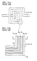
- the inventor of the present application has made studies of a new inductor structure that the uppermost interconnection layer is formed of aluminum, and an inductor is formed, including the aluminum interconnection layer.
- the inductor including the aluminum interconnection layer has new problems which has not taken place in inductors formed of only copper interconnection layers.
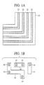
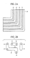
- the above-described contrivances for the pattern may be applied to the pattern of the copper interconnection below the groove-shaped vias. It is true with the damascene interconnection that the defective filling tends to occur at the corner of the groove-shaped vias.
- a width of the via-hole 4 6a may be suitably designed as described above.
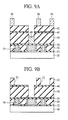
- the photoresist film 42 and the non-photosensitive resin 40 are removed by ashing using, e.g., oxygen plasma ( FIG. 9B ).
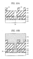
- the etching stopper film 60 is anisotropically etched to open the via-holes 66, 66a down onto the interconnection 58 ( FIG. 12A ).
- a 700 nm-thick silicon oxide film 84 and a 500 nm-thick silicon nitride film 86 are sequentially deposited by, e.g., CVD to form the cover film of the layer structure of the silicon nitride film 86/the silicon oxide film 86.
- the defective filling of the contact plug can be prevented, whereby resultantly the cracking of the inter-layer insulating film can be prevented. Steps on the contact plug can be reduced, so that the step cannot be influential on the upper interconnection layers and insulating layers. Accordingly, defective contact with the upper interconnection layer and the problems taking place in laying the films can be hindered.
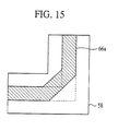
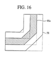
- the semiconductor device and the method for fabricating the same according to a second embodiment of the present invention will be explained with reference to FIGs. 15 and 16 .
- the same members of the present embodiment as those of the semiconductor device and the method for fabricating the same according to the first embodiment are represented by the same reference numbers not to repeat or to simplify their explanation.
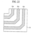
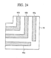
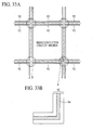
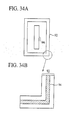
- the pattern of the groove-shaped via-hole 66a has the corner bent twice each time at 135°, whereby the corner is bent totally at 90°.
- the pattern of the via-hole 66a is thus designed, whereby a maximum width of the via-hole 66a can be made smaller in comparison with a maximum width the via-hole 66a is bent once by 90°.
- the generation of the defective filling of the contact plug 72a at the corner can be suppressed.
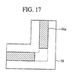
- FIG. 17 is a plan view of the design structure of the semiconductor device according to the present embodiment.
- the layout of the via-hole shown in FIG. 18 may be applied to the via-hole 46a, whereby the generation of the defective filling of the interconnection 58 can be suppressed.
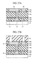
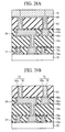
- film thickness conditions of the titanium nitride film 68 and the tungsten film 70 for forming the contact plugs 72 are respectively set to 50 nm and to 300 nm so as to sufficiently fill the via-holes 66.
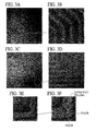
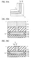
- film thickness conditions can completely fill the vial holes of a 0.7 ⁇ m-maximum width but cannot completely fill the via-hole 66a having a 0.8 ⁇ m-maximum width at the corner ( FIG. 29B ). Accordingly, when the contact plug 72a is formed later by polishing by CMP, the defective filling takes place at the central part of the plug ( FIGs. 29A and 29C ).
- film thickness conditions for forming the contact plugs are set in consideration of a maximum width of the groove-shaped via pattern, whereby even when a difference takes place in the finished size between the hole-shaped pattern and the groove-shaped pattern, the defective filling of the contact plug and the interconnection can be prevented. The cracking of the inter-layer insulating film due to the defective filling can be prevented.
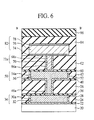
- FIG. 31 is a diagrammatic sectional view of the semiconductor device according to the present embodiment, which shows the structure thereof.
- FIG. 32 is a diagrammatic sectional view of the semiconductor device according to another example of the present embodiment, which shows the structure thereof.
- An inter-layer insulating film 134 of a layer film of a silicon oxide film/a silicon nitride film is formed on the inter-layer insulating film 130 with the interconnections 132 buried in.
- An inter-layer insulating film 136 of a layer film of a silicon oxide film/a silicon nitride film is formed on the inter-layer insulating film 134.
- Interconnections 138 of a layer structure of a copper film/a tantalum film are formed in the inter-layer insulating films 134, 136 with the via portion buried in the inter-layer insulating film 134 and the interconnection portion buried in the inter-layer insulating film 136.
- the present invention may be applicable to the step of forming the contact plugs 154. Accordingly, the defective filling of the contact plugs 154 can be prevented, and resultantly the cracking of the inter-layer insulating film 152 can be prevented. In the case that the defective filling of the copper interconnections takes place, the present invention may be applicable to the steps of forming the interconnections 120, 126, 132, 138, 144, 150. In the case that groove-shaped vias are used for the contact plugs 110, the defective filling of the contact plugs 110 can be also prevented.
- An inter-layer insulating film 224 of a layer film of an SiC film/a SiLK film/an SiC film is formed on the inter-layer insulating film 220 with the interconnections 222 buried in.
- Interconnections 226 of a layer structure of a copper film/a tantalum film and having the via portion and the interconnection portion are buried in the inter-layer insulating film 224.
- An inter-layer insulating film 258 of a layer film of a silicon oxide film/an SiC film is formed on the inter-layer insulating film 254 with the interconnections 256 buried in.
- An inter-layer insulating film 260 of a layer film of a silicon oxide film/an SiC film is formed on the inter-layer insulating film 258.
- Interconnections 262 of a layer structure of a copper film/a tantalum film are formed in the inter-layer insulating films 258, 260 with the via portion buried in the inter-layer insulating film 258 and the interconnection portion buried in the inter-layer insulating film 260.
- An inter-layer insulating film 264 of a layer film of a silicon oxide film/an SiC film is formed on the inter-layer insulating film 260 with the interconnections 262 buried in.
- Contact plugs 266 of a layer structure of a tungsten film/a titanium nitride film are buried in the inter-layer insulating film 264.
Landscapes
- Internal Circuitry In Semiconductor Integrated Circuit Devices (AREA)
- Physics & Mathematics (AREA)
- Geometry (AREA)
- Semiconductor Integrated Circuits (AREA)
Priority Applications (1)
| Application Number | Priority Date | Filing Date | Title |
|---|---|---|---|
| EP17156454.5A EP3208846B1 (fr) | 2002-07-31 | 2003-07-24 | Dispositif semi-conducteur |
Applications Claiming Priority (3)
| Application Number | Priority Date | Filing Date | Title |
|---|---|---|---|
| JP2002223343A JP3779243B2 (ja) | 2002-07-31 | 2002-07-31 | 半導体装置及びその製造方法 |
| EP20100000804 EP2175487B8 (fr) | 2002-07-31 | 2003-07-24 | Dispositif à semi-conducteur |
| EP03016553A EP1387404B1 (fr) | 2002-07-31 | 2003-07-24 | Dispositif à semi-conducteur |
Related Parent Applications (3)
| Application Number | Title | Priority Date | Filing Date |
|---|---|---|---|
| EP03016553A Division EP1387404B1 (fr) | 2002-07-31 | 2003-07-24 | Dispositif à semi-conducteur |
| EP20100000804 Division EP2175487B8 (fr) | 2002-07-31 | 2003-07-24 | Dispositif à semi-conducteur |
| EP20100000804 Division-Into EP2175487B8 (fr) | 2002-07-31 | 2003-07-24 | Dispositif à semi-conducteur |
Related Child Applications (2)
| Application Number | Title | Priority Date | Filing Date |
|---|---|---|---|
| EP17156454.5A Division-Into EP3208846B1 (fr) | 2002-07-31 | 2003-07-24 | Dispositif semi-conducteur |
| EP17156454.5A Division EP3208846B1 (fr) | 2002-07-31 | 2003-07-24 | Dispositif semi-conducteur |
Publications (3)
| Publication Number | Publication Date |
|---|---|
| EP2863430A2 true EP2863430A2 (fr) | 2015-04-22 |
| EP2863430A3 EP2863430A3 (fr) | 2015-07-22 |
| EP2863430B1 EP2863430B1 (fr) | 2017-04-12 |
Family
ID=30112961
Family Applications (6)
| Application Number | Title | Priority Date | Filing Date |
|---|---|---|---|
| EP15150443.8A Expired - Lifetime EP2863431B1 (fr) | 2002-07-31 | 2003-07-24 | Dispositif semi-conducteur |
| EP17156454.5A Expired - Lifetime EP3208846B1 (fr) | 2002-07-31 | 2003-07-24 | Dispositif semi-conducteur |
| EP20100000803 Expired - Lifetime EP2175486B1 (fr) | 2002-07-31 | 2003-07-24 | Dispositif à semi-conducteur et son procédé de fabrication |
| EP20100000804 Expired - Lifetime EP2175487B8 (fr) | 2002-07-31 | 2003-07-24 | Dispositif à semi-conducteur |
| EP03016553A Expired - Lifetime EP1387404B1 (fr) | 2002-07-31 | 2003-07-24 | Dispositif à semi-conducteur |
| EP15150440.4A Expired - Lifetime EP2863430B1 (fr) | 2002-07-31 | 2003-07-24 | Dispositif semi-conducteur |
Family Applications Before (5)
| Application Number | Title | Priority Date | Filing Date |
|---|---|---|---|
| EP15150443.8A Expired - Lifetime EP2863431B1 (fr) | 2002-07-31 | 2003-07-24 | Dispositif semi-conducteur |
| EP17156454.5A Expired - Lifetime EP3208846B1 (fr) | 2002-07-31 | 2003-07-24 | Dispositif semi-conducteur |
| EP20100000803 Expired - Lifetime EP2175486B1 (fr) | 2002-07-31 | 2003-07-24 | Dispositif à semi-conducteur et son procédé de fabrication |
| EP20100000804 Expired - Lifetime EP2175487B8 (fr) | 2002-07-31 | 2003-07-24 | Dispositif à semi-conducteur |
| EP03016553A Expired - Lifetime EP1387404B1 (fr) | 2002-07-31 | 2003-07-24 | Dispositif à semi-conducteur |
Country Status (7)
| Country | Link |
|---|---|
| US (31) | US7301241B2 (fr) |
| EP (6) | EP2863431B1 (fr) |
| JP (1) | JP3779243B2 (fr) |
| KR (1) | KR100917455B1 (fr) |
| CN (1) | CN1294653C (fr) |
| DE (1) | DE60331799D1 (fr) |
| TW (1) | TWI223399B (fr) |
Cited By (1)
| Publication number | Priority date | Publication date | Assignee | Title |
|---|---|---|---|---|
| CN106684046A (zh) * | 2015-11-11 | 2017-05-17 | 无锡华润上华半导体有限公司 | 一种降低多晶高阻的氢化作用的结构、方法及半导体器件 |
Families Citing this family (74)
| Publication number | Priority date | Publication date | Assignee | Title |
|---|---|---|---|---|
| US7271489B2 (en) * | 2003-10-15 | 2007-09-18 | Megica Corporation | Post passivation interconnection schemes on top of the IC chips |
| JP3779243B2 (ja) * | 2002-07-31 | 2006-05-24 | 富士通株式会社 | 半導体装置及びその製造方法 |
| US7400025B2 (en) * | 2003-05-21 | 2008-07-15 | Texas Instruments Incorporated | Integrated circuit inductor with integrated vias |
| US7198409B2 (en) * | 2003-06-30 | 2007-04-03 | Adc Telecommunications, Inc. | Fiber optic connector holder and method |
| JP4725092B2 (ja) * | 2004-12-10 | 2011-07-13 | ソニー株式会社 | 固体撮像装置及びその製造方法 |
| US7323784B2 (en) * | 2005-03-17 | 2008-01-29 | Taiwan Semiconductor Manufacturing Co., Ltd. | Top via pattern for bond pad structure |
| JP2007019188A (ja) | 2005-07-06 | 2007-01-25 | Renesas Technology Corp | 半導体集積回路装置およびその製造方法 |
| KR100632467B1 (ko) * | 2005-08-12 | 2006-10-09 | 삼성전자주식회사 | 반도체 메모리 소자 및 그 제조 방법 |
| JP5038612B2 (ja) | 2005-09-29 | 2012-10-03 | 富士通セミコンダクター株式会社 | 半導体装置 |
| KR100650907B1 (ko) * | 2005-12-29 | 2006-11-28 | 동부일렉트로닉스 주식회사 | 구리 금속으로 된 집적회로 인덕터 및 그 제조 방법 |
| US7459792B2 (en) * | 2006-06-19 | 2008-12-02 | Taiwan Semiconductor Manufacturing Co., Ltd. | Via layout with via groups placed in interlocked arrangement |
| KR100737155B1 (ko) * | 2006-08-28 | 2007-07-06 | 동부일렉트로닉스 주식회사 | 반도체 소자의 고주파 인덕터 제조 방법 |
| US20080067554A1 (en) * | 2006-09-14 | 2008-03-20 | Jae-Hun Jeong | NAND flash memory device with 3-dimensionally arranged memory cell transistors |
| US20080099884A1 (en) * | 2006-10-31 | 2008-05-01 | Masahio Inohara | Staggered guard ring structure |
| KR100995558B1 (ko) * | 2007-03-22 | 2010-11-22 | 후지쯔 세미컨덕터 가부시키가이샤 | 반도체 장치 및 반도체 장치의 제조 방법 |
| JP5332200B2 (ja) * | 2007-03-22 | 2013-11-06 | 富士通セミコンダクター株式会社 | 半導体装置及び半導体装置の製造方法 |
| US8030733B1 (en) | 2007-05-22 | 2011-10-04 | National Semiconductor Corporation | Copper-compatible fuse target |
| US7964934B1 (en) | 2007-05-22 | 2011-06-21 | National Semiconductor Corporation | Fuse target and method of forming the fuse target in a copper process flow |
| KR100946024B1 (ko) * | 2007-09-06 | 2010-03-09 | 주식회사 하이닉스반도체 | 반도체 소자의 금속 배선 및 그것의 형성 방법 |
| US20090079083A1 (en) * | 2007-09-26 | 2009-03-26 | United Microelectronics Corp. | Interconnect structure and fabricating method of the same |
| JP5411436B2 (ja) * | 2008-03-04 | 2014-02-12 | セミコンダクター・コンポーネンツ・インダストリーズ・リミテッド・ライアビリティ・カンパニー | 集積回路及びその製造方法 |
| JP5324833B2 (ja) * | 2008-06-16 | 2013-10-23 | ルネサスエレクトロニクス株式会社 | 半導体装置 |
| US9287438B1 (en) * | 2008-07-16 | 2016-03-15 | Solaero Technologies Corp. | Method for forming ohmic N-contacts at low temperature in inverted metamorphic multijunction solar cells with contaminant isolation |
| US7709956B2 (en) * | 2008-09-15 | 2010-05-04 | National Semiconductor Corporation | Copper-topped interconnect structure that has thin and thick copper traces and method of forming the copper-topped interconnect structure |
| JP2010108966A (ja) * | 2008-10-28 | 2010-05-13 | Elpida Memory Inc | 半導体装置及び半導体装置の製造方法 |
| JP2010141097A (ja) * | 2008-12-11 | 2010-06-24 | Panasonic Corp | 半導体装置及びその製造方法 |
| US8630033B2 (en) | 2008-12-23 | 2014-01-14 | Silex Microsystems Ab | Via structure and method thereof |
| SE533992C2 (sv) | 2008-12-23 | 2011-03-22 | Silex Microsystems Ab | Elektrisk anslutning i en struktur med isolerande och ledande lager |
| US20100314765A1 (en) * | 2009-06-16 | 2010-12-16 | Liang Wen-Ping | Interconnection structure of semiconductor integrated circuit and method for making the same |
| JP5460141B2 (ja) * | 2009-06-26 | 2014-04-02 | ラピスセミコンダクタ株式会社 | 半導体装置 |
| JP2011014610A (ja) * | 2009-06-30 | 2011-01-20 | Toshiba Corp | 半導体記憶装置 |
| US8314472B2 (en) | 2010-07-29 | 2012-11-20 | Avago Technologies Wireless Ip (Singapore) Pte. Ltd. | Semiconductor structure comprising pillar |
| US8344504B2 (en) | 2010-07-29 | 2013-01-01 | Avago Technologies Wireless Ip (Singapore) Pte. Ltd. | Semiconductor structure comprising pillar and moisture barrier |
| KR101143637B1 (ko) * | 2010-11-18 | 2012-05-09 | 에스케이하이닉스 주식회사 | 내부 연결 구조를 포함하는 반도체 소자 |
| CN102324427B (zh) * | 2011-10-20 | 2016-03-16 | 上海集成电路研发中心有限公司 | 一种金属薄膜电阻结构及其制造方法 |
| US8536707B2 (en) | 2011-11-29 | 2013-09-17 | Avago Technologies General Ip (Singapore) Pte. Ltd. | Semiconductor structure comprising moisture barrier and conductive redistribution layer |
| JP5802534B2 (ja) * | 2011-12-06 | 2015-10-28 | 株式会社東芝 | 半導体装置 |
| US8994178B2 (en) | 2012-03-29 | 2015-03-31 | Taiwan Semiconductor Manufacturing Company, Ltd. | Interconnect structure and method for forming the same |
| SE538058C2 (sv) * | 2012-03-30 | 2016-02-23 | Silex Microsystems Ab | Metod att tillhandahålla ett viahål och en routing-struktur |
| US8877628B2 (en) | 2012-07-12 | 2014-11-04 | Micron Technologies, Inc. | Methods of forming nano-scale pores, nano-scale electrical contacts, and memory devices including nano-scale electrical contacts, and related structures and devices |
| US8754508B2 (en) * | 2012-08-29 | 2014-06-17 | Taiwan Semiconductor Manufacturing Company, Ltd. | Structure to increase resistance to electromigration |
| US8871634B2 (en) * | 2012-08-30 | 2014-10-28 | Intel Corporation | Chip package incorporating interfacial adhesion through conductor sputtering |
| WO2014109044A1 (fr) * | 2013-01-11 | 2014-07-17 | ルネサスエレクトロニクス株式会社 | Dispositif à semi-conducteurs |
| US8793627B1 (en) * | 2013-03-15 | 2014-07-29 | Globalfoundries Inc. | Via non-standard limiting parameters |
| US9524950B2 (en) | 2013-05-31 | 2016-12-20 | Freescale Semiconductor, Inc. | Stacked microelectronic packages having sidewall conductors and methods for the fabrication thereof |
| US9577023B2 (en) | 2013-06-04 | 2017-02-21 | Globalfoundries Inc. | Metal wires of a stacked inductor |
| US9251948B2 (en) * | 2013-07-24 | 2016-02-02 | International Business Machines Corporation | High efficiency on-chip 3D transformer structure |
| US9831026B2 (en) | 2013-07-24 | 2017-11-28 | Globalfoundries Inc. | High efficiency on-chip 3D transformer structure |
| US9171663B2 (en) | 2013-07-25 | 2015-10-27 | Globalfoundries U.S. 2 Llc | High efficiency on-chip 3D transformer structure |
| US9779869B2 (en) | 2013-07-25 | 2017-10-03 | International Business Machines Corporation | High efficiency on-chip 3D transformer structure |
| US9263420B2 (en) * | 2013-12-05 | 2016-02-16 | Freescale Semiconductor, Inc. | Devices and stacked microelectronic packages with package surface conductors and methods of their fabrication |
| US10388607B2 (en) | 2014-12-17 | 2019-08-20 | Nxp Usa, Inc. | Microelectronic devices with multi-layer package surface conductors and methods of their fabrication |
| CN107004598B (zh) * | 2014-12-23 | 2021-03-19 | 英特尔公司 | 过孔阻挡层 |
| US9583438B2 (en) * | 2014-12-26 | 2017-02-28 | Taiwan Semiconductor Manufacturing Company Ltd. | Interconnect structure with misaligned metal lines coupled using different interconnect layer |
| US9818729B1 (en) * | 2016-06-16 | 2017-11-14 | Taiwan Semiconductor Manufacturing Company, Ltd. | Package-on-package structure and method |
| KR20180006740A (ko) * | 2016-07-11 | 2018-01-19 | 에스케이하이닉스 주식회사 | 반도체 소자 및 그 제조 방법 |
| KR102307127B1 (ko) * | 2017-06-14 | 2021-10-05 | 삼성전자주식회사 | 반도체 소자 |
| US10643006B2 (en) * | 2017-06-14 | 2020-05-05 | International Business Machines Corporation | Semiconductor chip including integrated security circuit |
| JP6806252B2 (ja) * | 2017-07-13 | 2021-01-06 | 富士電機株式会社 | 半導体装置 |
| DE102018108763A1 (de) | 2018-04-12 | 2019-10-17 | Hettich-Oni Gmbh & Co. Kg | Scharnier |
| DE102018111319A1 (de) | 2018-05-11 | 2019-11-14 | Osram Opto Semiconductors Gmbh | Optoelektronisches Halbleiterbauelement und Verfahren zur Herstellung eines optoelektronischen Halbleiterbauelements |
| CN208489194U (zh) * | 2018-05-23 | 2019-02-12 | 京东方科技集团股份有限公司 | 阵列基板、显示面板及显示装置 |
| US11545449B2 (en) * | 2018-06-25 | 2023-01-03 | Intel Corporation | Guard ring structure for an integrated circuit |
| CN109690776B (zh) | 2018-12-07 | 2020-01-10 | 长江存储科技有限责任公司 | 新型3d nand存储器件及其形成方法 |
| US11004805B2 (en) * | 2019-08-16 | 2021-05-11 | Winbond Electronics Corp. | Semiconductor device and method of fabricating same including two seal rings |
| JP7290513B2 (ja) * | 2019-08-26 | 2023-06-13 | ルネサスエレクトロニクス株式会社 | 半導体装置 |
| US11728282B2 (en) * | 2019-10-17 | 2023-08-15 | Advanced Semiconductor Engineering, Inc. | Package structure, assembly structure and method for manufacturing the same |
| JP7284121B2 (ja) * | 2020-03-23 | 2023-05-30 | 株式会社東芝 | アイソレータ |
| CN113589638B (zh) * | 2020-04-30 | 2024-05-24 | 中芯国际集成电路制造(上海)有限公司 | 掩膜版版图和半导体结构 |
| KR20220028539A (ko) * | 2020-08-28 | 2022-03-08 | 에스케이하이닉스 주식회사 | 반도체 장치 |
| CN112447518A (zh) * | 2020-11-25 | 2021-03-05 | 绍兴同芯成集成电路有限公司 | 一种igbt晶圆的接触孔成形工艺 |
| CN113506786B (zh) * | 2021-07-08 | 2022-02-15 | 哈尔滨工业大学 | 一种适用于叠层式封装的层间连接线改良设计方法 |
| US12354975B2 (en) | 2021-11-23 | 2025-07-08 | Taiwan Semiconductor Manufacturing Company, Ltd. | Guard ring structure |
| US20240355728A1 (en) * | 2023-04-21 | 2024-10-24 | Taiwan Semiconductor Manufacturing Company, Ltd. | Semiconductor structure |
Citations (1)
| Publication number | Priority date | Publication date | Assignee | Title |
|---|---|---|---|---|
| JP2000124403A (ja) | 1998-10-12 | 2000-04-28 | Nec Corp | 半導体装置 |
Family Cites Families (63)
| Publication number | Priority date | Publication date | Assignee | Title |
|---|---|---|---|---|
| JPS6020578A (ja) * | 1983-07-15 | 1985-02-01 | Hitachi Ltd | 絶縁ゲ−ト半導体装置とその製造法 |
| JPS6223135A (ja) | 1985-07-24 | 1987-01-31 | Hitachi Micro Comput Eng Ltd | 半導体装置 |
| JPH0389548A (ja) | 1989-08-31 | 1991-04-15 | Fujitsu Ltd | 半導体集積回路 |
| JP3216161B2 (ja) | 1991-09-12 | 2001-10-09 | 日本電気株式会社 | 半導体装置 |
| JPH05175198A (ja) | 1991-12-25 | 1993-07-13 | Kawasaki Steel Corp | 半導体装置 |
| JP2823461B2 (ja) * | 1992-12-11 | 1998-11-11 | 三菱電機株式会社 | 高周波帯ic用パッケージ |
| JPH07201855A (ja) * | 1993-12-28 | 1995-08-04 | Fujitsu Ltd | 半導体装置 |
| US5559367A (en) * | 1994-07-12 | 1996-09-24 | International Business Machines Corporation | Diamond-like carbon for use in VLSI and ULSI interconnect systems |
| US5584320A (en) * | 1994-10-31 | 1996-12-17 | Cobe Laboratories, Inc. | Multi-tube clamp actuator and mating cartridge |
| US5521121A (en) * | 1995-04-03 | 1996-05-28 | Taiwan Semiconductor Manufacturing Company | Oxygen plasma etch process post contact layer etch back |
| US5981384A (en) * | 1995-08-14 | 1999-11-09 | Micron Technology, Inc. | Method of intermetal dielectric planarization by metal features layout modification |
| JPH09153545A (ja) * | 1995-09-29 | 1997-06-10 | Toshiba Corp | 半導体装置及びその製造方法 |
| JPH09312391A (ja) * | 1996-05-22 | 1997-12-02 | Toshiba Corp | 半導体装置およびその製造方法 |
| JP3526376B2 (ja) * | 1996-08-21 | 2004-05-10 | 株式会社東芝 | 半導体装置及びその製造方法 |
| US6349401B2 (en) * | 1996-09-12 | 2002-02-19 | Matsushita Electric Industrial Co., Ltd. | Semiconductor integrated circuit, design method and computer-readable medium using a permissive current ratio |
| TW325576B (en) * | 1996-12-12 | 1998-01-21 | Winbond Electronics Corp | The manufacturing methods for die seal |
| KR100444012B1 (ko) | 1997-05-08 | 2004-11-06 | 삼성전자주식회사 | 반도체칩의가드링(guard-ring) |
| US5895267A (en) * | 1997-07-09 | 1999-04-20 | Lsi Logic Corporation | Method to obtain a low resistivity and conformity chemical vapor deposition titanium film |
| JP3164025B2 (ja) | 1997-08-04 | 2001-05-08 | 日本電気株式会社 | 半導体集積回路装置及びその製造方法 |
| US6025221A (en) * | 1997-08-22 | 2000-02-15 | Micron Technology, Inc. | Processing methods of forming integrated circuitry memory devices, methods of forming DRAM arrays, and related semiconductor masks |
| JP3697044B2 (ja) * | 1997-12-19 | 2005-09-21 | 株式会社ルネサステクノロジ | 半導体集積回路装置およびその製造方法 |
| JP3500319B2 (ja) * | 1998-01-08 | 2004-02-23 | 太陽誘電株式会社 | 電子部品 |
| US5955781A (en) * | 1998-01-13 | 1999-09-21 | International Business Machines Corporation | Embedded thermal conductors for semiconductor chips |
| US6365958B1 (en) * | 1998-02-06 | 2002-04-02 | Texas Instruments Incorporated | Sacrificial structures for arresting insulator cracks in semiconductor devices |
| US5977571A (en) * | 1998-02-26 | 1999-11-02 | Lucent Technologies, Inc. | Low loss connecting arrangement for photodiodes |
| US6353242B1 (en) * | 1998-03-30 | 2002-03-05 | Kabushiki Kaisha Toshiba | Nonvolatile semiconductor memory |
| US5986343A (en) * | 1998-05-04 | 1999-11-16 | Lucent Technologies Inc. | Bond pad design for integrated circuits |
| US6483714B1 (en) * | 1999-02-24 | 2002-11-19 | Kyocera Corporation | Multilayered wiring board |
| US6956248B2 (en) * | 1999-03-01 | 2005-10-18 | Teccor Electronics, Lp | Semiconductor device for low voltage protection with low capacitance |
| US6531717B1 (en) * | 1999-03-01 | 2003-03-11 | Teccor Electronics, L.P. | Very low voltage actuated thyristor with centrally-located offset buried region |
| JP3502288B2 (ja) | 1999-03-19 | 2004-03-02 | 富士通株式会社 | 半導体装置およびその製造方法 |
| JP2000294625A (ja) | 1999-04-02 | 2000-10-20 | Sony Corp | 半導体装置 |
| US20020000665A1 (en) * | 1999-04-05 | 2002-01-03 | Alexander L. Barr | Semiconductor device conductive bump and interconnect barrier |
| JP2000311939A (ja) * | 1999-04-27 | 2000-11-07 | Mitsubishi Electric Corp | 半導体装置およびその製造方法 |
| US6365453B1 (en) * | 1999-06-16 | 2002-04-02 | Micron Technology, Inc. | Method and structure for reducing contact aspect ratios |
| JP2001007202A (ja) * | 1999-06-22 | 2001-01-12 | Sony Corp | 半導体装置の製造方法 |
| JP4122113B2 (ja) * | 1999-06-24 | 2008-07-23 | 新電元工業株式会社 | 高破壊耐量電界効果型トランジスタ |
| US6204557B1 (en) * | 1999-09-13 | 2001-03-20 | Integrated Device Technology, Inc. | Reduction of topside movement during temperature cycles |
| US6483176B2 (en) * | 1999-12-22 | 2002-11-19 | Kabushiki Kaisha Toshiba | Semiconductor with multilayer wiring structure that offer high speed performance |
| US6436763B1 (en) * | 2000-02-07 | 2002-08-20 | Taiwan Semiconductor Manufacturing Company | Process for making embedded DRAM circuits having capacitor under bit-line (CUB) |
| JP3386032B2 (ja) * | 2000-04-11 | 2003-03-10 | セイコーエプソン株式会社 | 半導体装置 |
| JP4979154B2 (ja) * | 2000-06-07 | 2012-07-18 | ルネサスエレクトロニクス株式会社 | 半導体装置 |
| US6362524B1 (en) * | 2000-07-26 | 2002-03-26 | Advanced Micro Devices, Inc. | Edge seal ring for copper damascene process and method for fabrication thereof |
| JP3917355B2 (ja) * | 2000-09-21 | 2007-05-23 | 株式会社東芝 | 半導体装置およびその製造方法 |
| US6555909B1 (en) * | 2001-01-11 | 2003-04-29 | Advanced Micro Devices, Inc. | Seedless barrier layers in integrated circuits and a method of manufacture therefor |
| US6709945B2 (en) * | 2001-01-16 | 2004-03-23 | Micron Technology, Inc. | Reduced aspect ratio digit line contact process flow used during the formation of a semiconductor device |
| JP3506676B2 (ja) * | 2001-01-25 | 2004-03-15 | Necエレクトロニクス株式会社 | 半導体装置 |
| JP4118029B2 (ja) * | 2001-03-09 | 2008-07-16 | 富士通株式会社 | 半導体集積回路装置とその製造方法 |
| US20020167071A1 (en) * | 2001-05-10 | 2002-11-14 | Mu-Chun Wang | Guard ring for protecting integrated circuits |
| FR2824954A1 (fr) * | 2001-05-18 | 2002-11-22 | St Microelectronics Sa | Plot de connexion d'un circuit integre |
| TW518680B (en) * | 2001-06-13 | 2003-01-21 | Matsushita Electric Industrial Co Ltd | Semiconductor device and method for fabricating the same |
| JP2003031575A (ja) * | 2001-07-17 | 2003-01-31 | Nec Corp | 半導体装置及びその製造方法 |
| JP3538170B2 (ja) | 2001-09-11 | 2004-06-14 | 松下電器産業株式会社 | 半導体装置及びその製造方法 |
| US6605874B2 (en) * | 2001-12-19 | 2003-08-12 | Intel Corporation | Method of making semiconductor device using an interconnect |
| EP2259325B1 (fr) * | 2002-02-20 | 2013-12-25 | Shindengen Electric Manufacturing Co., Ltd. | Dispositif de transistor |
| JP3914785B2 (ja) * | 2002-02-20 | 2007-05-16 | 新電元工業株式会社 | ダイオード素子 |
| US6841825B2 (en) * | 2002-06-05 | 2005-01-11 | Shindengen Electric Manufacturing Co., Ltd. | Semiconductor device |
| JP4274771B2 (ja) * | 2002-10-04 | 2009-06-10 | 新電元工業株式会社 | 半導体装置 |
| JP3779243B2 (ja) * | 2002-07-31 | 2006-05-24 | 富士通株式会社 | 半導体装置及びその製造方法 |
| JP4177798B2 (ja) * | 2004-08-23 | 2008-11-05 | 株式会社東芝 | 半導体装置 |
| JP2006210439A (ja) * | 2005-01-25 | 2006-08-10 | Nec Electronics Corp | 半導体装置 |
| JP4699172B2 (ja) * | 2005-10-25 | 2011-06-08 | ルネサスエレクトロニクス株式会社 | 半導体装置 |
| US7485912B2 (en) * | 2006-03-28 | 2009-02-03 | Taiwan Semiconductor Manufacturing Company, Ltd. | Flexible metal-oxide-metal capacitor design |
-
2002
- 2002-07-31 JP JP2002223343A patent/JP3779243B2/ja not_active Expired - Lifetime
-
2003
- 2003-07-21 US US10/622,614 patent/US7301241B2/en not_active Expired - Lifetime
- 2003-07-24 EP EP15150443.8A patent/EP2863431B1/fr not_active Expired - Lifetime
- 2003-07-24 EP EP17156454.5A patent/EP3208846B1/fr not_active Expired - Lifetime
- 2003-07-24 EP EP20100000803 patent/EP2175486B1/fr not_active Expired - Lifetime
- 2003-07-24 EP EP20100000804 patent/EP2175487B8/fr not_active Expired - Lifetime
- 2003-07-24 DE DE60331799T patent/DE60331799D1/de not_active Expired - Lifetime
- 2003-07-24 EP EP03016553A patent/EP1387404B1/fr not_active Expired - Lifetime
- 2003-07-24 EP EP15150440.4A patent/EP2863430B1/fr not_active Expired - Lifetime
- 2003-07-25 KR KR1020030051297A patent/KR100917455B1/ko not_active Expired - Lifetime
- 2003-07-28 TW TW092120527A patent/TWI223399B/zh not_active IP Right Cessation
- 2003-07-31 CN CNB031523986A patent/CN1294653C/zh not_active Expired - Lifetime
-
2005
- 2005-06-02 US US11/142,407 patent/US7446418B2/en not_active Expired - Lifetime
-
2007
- 2007-09-13 US US11/898,548 patent/US7906851B2/en not_active Expired - Lifetime
-
2010
- 2010-09-14 US US12/881,515 patent/US7932609B2/en not_active Expired - Lifetime
-
2011
- 2011-01-25 US US13/013,103 patent/US8410613B2/en not_active Expired - Fee Related
-
2012
- 2012-07-13 US US13/548,792 patent/US8633594B2/en not_active Expired - Fee Related
- 2012-07-13 US US13/549,006 patent/US8829681B2/en not_active Expired - Lifetime
- 2012-07-13 US US13/548,911 patent/US8791576B2/en not_active Expired - Lifetime
- 2012-07-13 US US13/548,966 patent/US8633595B2/en not_active Expired - Fee Related
- 2012-07-13 US US13/548,857 patent/US8872347B2/en not_active Expired - Lifetime
-
2013
- 2013-02-28 US US13/780,396 patent/US8847403B2/en not_active Expired - Lifetime
- 2013-02-28 US US13/780,236 patent/US8872352B2/en not_active Expired - Lifetime
- 2013-02-28 US US13/780,174 patent/US8853861B2/en not_active Expired - Lifetime
- 2013-02-28 US US13/780,311 patent/US8872353B2/en not_active Expired - Lifetime
- 2013-03-15 US US13/834,418 patent/US8841775B2/en not_active Expired - Lifetime
- 2013-11-20 US US14/085,124 patent/US20140077392A1/en not_active Abandoned
-
2014
- 2014-01-31 US US14/169,717 patent/US9082771B2/en not_active Expired - Lifetime
- 2014-01-31 US US14/169,649 patent/US9105640B2/en not_active Expired - Lifetime
- 2014-06-13 US US14/304,225 patent/US9412697B2/en not_active Expired - Fee Related
- 2014-06-13 US US14/304,088 patent/US9412696B2/en not_active Expired - Fee Related
- 2014-06-13 US US14/304,139 patent/US9406610B2/en not_active Expired - Fee Related
- 2014-06-13 US US14/304,186 patent/US9406611B2/en not_active Expired - Fee Related
- 2014-06-20 US US14/310,680 patent/US9224690B2/en not_active Expired - Lifetime
- 2014-06-20 US US14/310,612 patent/US9502353B2/en not_active Expired - Fee Related
- 2014-06-20 US US14/310,244 patent/US9412698B2/en not_active Expired - Fee Related
- 2014-06-20 US US14/310,338 patent/US9224689B2/en not_active Expired - Lifetime
- 2014-06-24 US US14/313,010 patent/US9406613B2/en not_active Expired - Fee Related
- 2014-06-24 US US14/312,867 patent/US9406612B2/en not_active Expired - Fee Related
- 2014-06-24 US US14/313,024 patent/US9412699B2/en not_active Expired - Fee Related
-
2016
- 2016-10-12 US US15/291,593 patent/US9972531B2/en not_active Expired - Lifetime
-
2018
- 2018-04-11 US US15/950,201 patent/US10403543B2/en not_active Expired - Lifetime
Patent Citations (1)
| Publication number | Priority date | Publication date | Assignee | Title |
|---|---|---|---|---|
| JP2000124403A (ja) | 1998-10-12 | 2000-04-28 | Nec Corp | 半導体装置 |
Cited By (2)
| Publication number | Priority date | Publication date | Assignee | Title |
|---|---|---|---|---|
| CN106684046A (zh) * | 2015-11-11 | 2017-05-17 | 无锡华润上华半导体有限公司 | 一种降低多晶高阻的氢化作用的结构、方法及半导体器件 |
| CN106684046B (zh) * | 2015-11-11 | 2019-03-08 | 无锡华润上华科技有限公司 | 一种降低多晶高阻的氢化作用的结构、方法及半导体器件 |
Also Published As
Similar Documents
| Publication | Publication Date | Title |
|---|---|---|
| US10403543B2 (en) | Semiconductor device having groove-shaped via-hole |
Legal Events
| Date | Code | Title | Description |
|---|---|---|---|
| PUAI | Public reference made under article 153(3) epc to a published international application that has entered the european phase |
Free format text: ORIGINAL CODE: 0009012 |
|
| 17P | Request for examination filed |
Effective date: 20150108 |
|
| AC | Divisional application: reference to earlier application |
Ref document number: 1387404 Country of ref document: EP Kind code of ref document: P Ref document number: 2175487 Country of ref document: EP Kind code of ref document: P |
|
| AK | Designated contracting states |
Kind code of ref document: A2 Designated state(s): DE FR IT |
|
| RAP1 | Party data changed (applicant data changed or rights of an application transferred) |
Owner name: SOCIONEXT INC. |
|
| PUAL | Search report despatched |
Free format text: ORIGINAL CODE: 0009013 |
|
| AK | Designated contracting states |
Kind code of ref document: A3 Designated state(s): DE FR IT |
|
| RIC1 | Information provided on ipc code assigned before grant |
Ipc: H01L 23/58 20060101ALI20150617BHEP Ipc: H01L 23/532 20060101ALI20150617BHEP Ipc: H01L 23/528 20060101ALI20150617BHEP Ipc: H01L 23/522 20060101AFI20150617BHEP |
|
| R17P | Request for examination filed (corrected) |
Effective date: 20151221 |
|
| RBV | Designated contracting states (corrected) |
Designated state(s): DE FR IT |
|
| 17Q | First examination report despatched |
Effective date: 20160421 |
|
| GRAP | Despatch of communication of intention to grant a patent |
Free format text: ORIGINAL CODE: EPIDOSNIGR1 |
|
| INTG | Intention to grant announced |
Effective date: 20161031 |
|
| RIN1 | Information on inventor provided before grant (corrected) |
Inventor name: WATANABE, KENICHI |
|
| GRAS | Grant fee paid |
Free format text: ORIGINAL CODE: EPIDOSNIGR3 |
|
| GRAA | (expected) grant |
Free format text: ORIGINAL CODE: 0009210 |
|
| AC | Divisional application: reference to earlier application |
Ref document number: 2175487 Country of ref document: EP Kind code of ref document: P Ref document number: 1387404 Country of ref document: EP Kind code of ref document: P |
|
| AK | Designated contracting states |
Kind code of ref document: B1 Designated state(s): DE FR IT |
|
| REG | Reference to a national code |
Ref country code: DE Ref legal event code: R096 Ref document number: 60350125 Country of ref document: DE |
|
| REG | Reference to a national code |
Ref country code: DE Ref legal event code: R097 Ref document number: 60350125 Country of ref document: DE |
|
| PLBE | No opposition filed within time limit |
Free format text: ORIGINAL CODE: 0009261 |
|
| STAA | Information on the status of an ep patent application or granted ep patent |
Free format text: STATUS: NO OPPOSITION FILED WITHIN TIME LIMIT |
|
| PG25 | Lapsed in a contracting state [announced via postgrant information from national office to epo] |
Ref country code: IT Free format text: LAPSE BECAUSE OF FAILURE TO SUBMIT A TRANSLATION OF THE DESCRIPTION OR TO PAY THE FEE WITHIN THE PRESCRIBED TIME-LIMIT Effective date: 20170412 |
|
| 26N | No opposition filed |
Effective date: 20180115 |
|
| REG | Reference to a national code |
Ref country code: FR Ref legal event code: ST Effective date: 20180330 |
|
| PG25 | Lapsed in a contracting state [announced via postgrant information from national office to epo] |
Ref country code: FR Free format text: LAPSE BECAUSE OF NON-PAYMENT OF DUE FEES Effective date: 20170731 |
|
| PGFP | Annual fee paid to national office [announced via postgrant information from national office to epo] |
Ref country code: DE Payment date: 20220720 Year of fee payment: 20 |
|
| REG | Reference to a national code |
Ref country code: DE Ref legal event code: R071 Ref document number: 60350125 Country of ref document: DE |