EP2874005A2 - Verfahren zum Aufbringen eines Bildes, und entsprechende Unterlage - Google Patents
Verfahren zum Aufbringen eines Bildes, und entsprechende Unterlage Download PDFInfo
- Publication number
- EP2874005A2 EP2874005A2 EP20140186497 EP14186497A EP2874005A2 EP 2874005 A2 EP2874005 A2 EP 2874005A2 EP 20140186497 EP20140186497 EP 20140186497 EP 14186497 A EP14186497 A EP 14186497A EP 2874005 A2 EP2874005 A2 EP 2874005A2
- Authority
- EP
- European Patent Office
- Prior art keywords
- opaque
- image
- opaque layer
- cell
- etched
- Prior art date
- Legal status (The legal status is an assumption and is not a legal conclusion. Google has not performed a legal analysis and makes no representation as to the accuracy of the status listed.)
- Withdrawn
Links
- 238000000034 method Methods 0.000 title claims abstract description 87
- 239000000758 substrate Substances 0.000 claims abstract description 73
- 238000005530 etching Methods 0.000 claims abstract description 49
- 239000011159 matrix material Substances 0.000 claims abstract description 28
- 238000000151 deposition Methods 0.000 claims abstract description 23
- 238000000206 photolithography Methods 0.000 claims description 52
- 238000012216 screening Methods 0.000 claims description 20
- 239000000463 material Substances 0.000 claims description 15
- 238000009432 framing Methods 0.000 claims description 13
- 238000000354 decomposition reaction Methods 0.000 claims description 11
- 230000008021 deposition Effects 0.000 claims description 8
- 238000005286 illumination Methods 0.000 claims 1
- 239000010410 layer Substances 0.000 description 224
- 230000033458 reproduction Effects 0.000 description 32
- 230000005540 biological transmission Effects 0.000 description 31
- MUMZUERVLWJKNR-UHFFFAOYSA-N oxoplatinum Chemical compound [Pt]=O MUMZUERVLWJKNR-UHFFFAOYSA-N 0.000 description 12
- 229910003446 platinum oxide Inorganic materials 0.000 description 12
- 239000012780 transparent material Substances 0.000 description 12
- 230000003287 optical effect Effects 0.000 description 9
- 238000003860 storage Methods 0.000 description 7
- 238000001514 detection method Methods 0.000 description 6
- VYPSYNLAJGMNEJ-UHFFFAOYSA-N silicon dioxide Inorganic materials O=[Si]=O VYPSYNLAJGMNEJ-UHFFFAOYSA-N 0.000 description 6
- 230000000694 effects Effects 0.000 description 5
- 238000006073 displacement reaction Methods 0.000 description 4
- 230000010070 molecular adhesion Effects 0.000 description 4
- 238000004026 adhesive bonding Methods 0.000 description 3
- 239000003086 colorant Substances 0.000 description 3
- 150000001875 compounds Chemical class 0.000 description 3
- 239000011347 resin Substances 0.000 description 3
- 229920005989 resin Polymers 0.000 description 3
- 229910004298 SiO 2 Inorganic materials 0.000 description 2
- 238000009792 diffusion process Methods 0.000 description 2
- 239000011521 glass Substances 0.000 description 2
- 238000009434 installation Methods 0.000 description 2
- JEIPFZHSYJVQDO-UHFFFAOYSA-N iron(III) oxide Inorganic materials O=[Fe]O[Fe]=O JEIPFZHSYJVQDO-UHFFFAOYSA-N 0.000 description 2
- BASFCYQUMIYNBI-UHFFFAOYSA-N platinum Chemical compound [Pt] BASFCYQUMIYNBI-UHFFFAOYSA-N 0.000 description 2
- 239000010453 quartz Substances 0.000 description 2
- 229910052594 sapphire Inorganic materials 0.000 description 2
- 239000010980 sapphire Substances 0.000 description 2
- 239000000377 silicon dioxide Substances 0.000 description 2
- 239000002356 single layer Substances 0.000 description 2
- 229910018072 Al 2 O 3 Inorganic materials 0.000 description 1
- VYZAMTAEIAYCRO-UHFFFAOYSA-N Chromium Chemical compound [Cr] VYZAMTAEIAYCRO-UHFFFAOYSA-N 0.000 description 1
- 241001080024 Telles Species 0.000 description 1
- NRTOMJZYCJJWKI-UHFFFAOYSA-N Titanium nitride Chemical compound [Ti]#N NRTOMJZYCJJWKI-UHFFFAOYSA-N 0.000 description 1
- 240000008042 Zea mays Species 0.000 description 1
- 230000001174 ascending effect Effects 0.000 description 1
- 230000008033 biological extinction Effects 0.000 description 1
- 230000015572 biosynthetic process Effects 0.000 description 1
- 239000000969 carrier Substances 0.000 description 1
- 229910052804 chromium Inorganic materials 0.000 description 1
- 239000011651 chromium Substances 0.000 description 1
- 230000007547 defect Effects 0.000 description 1
- 238000010586 diagram Methods 0.000 description 1
- 229920002457 flexible plastic Polymers 0.000 description 1
- 238000001459 lithography Methods 0.000 description 1
- 230000007774 longterm Effects 0.000 description 1
- 238000004519 manufacturing process Methods 0.000 description 1
- 230000000873 masking effect Effects 0.000 description 1
- 229910052751 metal Inorganic materials 0.000 description 1
- 239000002184 metal Substances 0.000 description 1
- TWNQGVIAIRXVLR-UHFFFAOYSA-N oxo(oxoalumanyloxy)alumane Chemical compound O=[Al]O[Al]=O TWNQGVIAIRXVLR-UHFFFAOYSA-N 0.000 description 1
- 229920002120 photoresistant polymer Polymers 0.000 description 1
- 229920003023 plastic Polymers 0.000 description 1
- 230000010287 polarization Effects 0.000 description 1
- 238000011084 recovery Methods 0.000 description 1
Images


Classifications
-
- G—PHYSICS
- G03—PHOTOGRAPHY; CINEMATOGRAPHY; ANALOGOUS TECHNIQUES USING WAVES OTHER THAN OPTICAL WAVES; ELECTROGRAPHY; HOLOGRAPHY
- G03F—PHOTOMECHANICAL PRODUCTION OF TEXTURED OR PATTERNED SURFACES, e.g. FOR PRINTING, FOR PROCESSING OF SEMICONDUCTOR DEVICES; MATERIALS THEREFOR; ORIGINALS THEREFOR; APPARATUS SPECIALLY ADAPTED THEREFOR
- G03F7/00—Photomechanical, e.g. photolithographic, production of textured or patterned surfaces, e.g. printing surfaces; Materials therefor, e.g. comprising photoresists; Apparatus specially adapted therefor
- G03F7/20—Exposure; Apparatus therefor
- G03F7/2022—Multi-step exposure, e.g. hybrid; backside exposure; blanket exposure, e.g. for image reversal; edge exposure, e.g. for edge bead removal; corrective exposure
-
- G—PHYSICS
- G03—PHOTOGRAPHY; CINEMATOGRAPHY; ANALOGOUS TECHNIQUES USING WAVES OTHER THAN OPTICAL WAVES; ELECTROGRAPHY; HOLOGRAPHY
- G03F—PHOTOMECHANICAL PRODUCTION OF TEXTURED OR PATTERNED SURFACES, e.g. FOR PRINTING, FOR PROCESSING OF SEMICONDUCTOR DEVICES; MATERIALS THEREFOR; ORIGINALS THEREFOR; APPARATUS SPECIALLY ADAPTED THEREFOR
- G03F7/00—Photomechanical, e.g. photolithographic, production of textured or patterned surfaces, e.g. printing surfaces; Materials therefor, e.g. comprising photoresists; Apparatus specially adapted therefor
- G03F7/12—Production of screen printing forms or similar printing forms, e.g. stencils
-
- G—PHYSICS
- G03—PHOTOGRAPHY; CINEMATOGRAPHY; ANALOGOUS TECHNIQUES USING WAVES OTHER THAN OPTICAL WAVES; ELECTROGRAPHY; HOLOGRAPHY
- G03F—PHOTOMECHANICAL PRODUCTION OF TEXTURED OR PATTERNED SURFACES, e.g. FOR PRINTING, FOR PROCESSING OF SEMICONDUCTOR DEVICES; MATERIALS THEREFOR; ORIGINALS THEREFOR; APPARATUS SPECIALLY ADAPTED THEREFOR
- G03F7/00—Photomechanical, e.g. photolithographic, production of textured or patterned surfaces, e.g. printing surfaces; Materials therefor, e.g. comprising photoresists; Apparatus specially adapted therefor
- G03F7/20—Exposure; Apparatus therefor
- G03F7/2051—Exposure without an original mask, e.g. using a programmed deflection of a point source, by scanning, by drawing with a light beam, using an addressed light or corpuscular source
-
- G—PHYSICS
- G11—INFORMATION STORAGE
- G11B—INFORMATION STORAGE BASED ON RELATIVE MOVEMENT BETWEEN RECORD CARRIER AND TRANSDUCER
- G11B7/00—Recording or reproducing by optical means, e.g. recording using a thermal beam of optical radiation by modifying optical properties or the physical structure, reproducing using an optical beam at lower power by sensing optical properties; Record carriers therefor
- G11B7/24—Record carriers characterised by shape, structure or physical properties, or by the selection of the material
- G11B7/26—Apparatus or processes specially adapted for the manufacture of record carriers
- G11B7/261—Preparing a master, e.g. exposing photoresist, electroforming
Definitions
- the present invention relates to the field of photolithographic inscription of an image on a support, and more particularly the field of image archiving methods.
- the archiving of an image here designates the storage of a reproduction of this image for later reading "by transparency”. It is usually a reproduction in reduced dimensions of this image, often in a single copy.
- image designates any graphic representation such as a photograph, a text, a table, a drawing, etc.
- the invention also relates to the field of image carriers made using such methods.
- the dithering step consists of converting a grayscale image into a black and white image, made of a matrix of cells of the same size, called “screening cells".
- the term "gray level" may also designate gradations of intensity of a color.
- frequency modulation screening is known in which each cell is homogeneous: entirely black or entirely white.
- Amplitude modulation dithering is also known in which each cell contains a shape of variable size written in white on black or in black on white.
- Figure 1A an image to archive.
- the Figure 1B represents this image after amplitude modulation dithering.
- the figure 1C represents this image after a framing by frequency modulation.
- the reading of the archiving medium is ensured by a low-pass filter which eliminates the fine variations of the screening structure below the cell scale, keeping only the evolutions averaged over a few cells.
- the archiving medium can for example be read by simple optical magnification means.
- the archiving medium 31 is illuminated by a light source 32.
- An optic 33 images the archiving medium 31 on a detector 34 such as a matrix detector.
- the optic 33 has an optical transfer function which introduces an optical blur comparable to a Gaussian spot width (we speak of "waist") equal to a few pixels, typically two or three.
- the magnification of the optics 33 is adapted to match the size of a screening cell with the pixel size of the matrix detector 34.
- the dark shades coded in the storage medium 31 are relative to the opaque layer and the hues clear to the etched openings in the opaque layer and releasing the surface of the transparent substrate.
- the image 35 is obtained on the matrix detector 34.
- a high-definition image is 8-bit encoded: each pixel in the image can take a gray level from 256 ( 28 ) available gray levels.
- the known solution is that one pixel of the image corresponds to a large number of screening cells.
- a disadvantage of such a solution is that the area of the archiving medium corresponding to this high definition image is increased.
- An object of the present invention is to provide a method of writing a source image, which does not present at least one of the disadvantages of the prior art.
- an object of the present invention is to provide a method of registering a source image by photolithography, which allows a compact writing of source images.
- an objective of the present invention is to propose a method of registering a source image by photolithography, which allows a compact writing of source images in high definition, typically a definition of at least 8 bits, for example 16 bits.
- Another object of the present invention is to provide an image support obtained using such a method.
- a layer of an opaque material, or opaque layer means a layer whose transmission coefficient is lower than that of the first substrate. This transmission coefficient can be zero, as long as it allows the formation of the elementary pattern obtained by the superimposed layers.
- the transmission coefficient is defined for the wavelengths of the visible, preferably between 400 nm and 800 nm.
- the first and second opaque layers preferably have respective degrees of opacity different from each other.
- the degree of opacity designates the rate or extinction coefficient, that is to say the inverse of the rate or transmission coefficient.
- the degree of opacity is preferably defined for the wavelengths of the visible, preferably between 400 nm and 800 nm.
- the first and second opaque layers preferably have different thicknesses and are formed by the same material. Opaque and first and second opaque layers are thus produced with respective degrees of opacity different from each other.
- first and second opaque layers may each consist of a different material. These materials advantageously have different properties of light transmission. It is thus possible to produce first and second opaque layers having the same thickness, and with respective degrees of opacity different from each other.
- the deposition of the second opaque layer is performed after the etching of the first opaque layer.
- the etching of the second opaque layer may be performed before or after deposition of the second opaque layer on the first etched opaque layer.
- an image to be decomposed is decomposed according to an HSV decomposition to obtain a "hue” component, a “saturation” component, and a “light intensity” component, the "hue” and “saturation” components are entered in the high definition archive area, and the "light intensity” component is entered in the low definition archive area.
- the first opaque layer and the second opaque layer may have different thicknesses, each thickness being between 10 nm and 200 nm.
- Each first cell and second cell may be either fully etched or ungraved.
- each first cell and second cell may be integrally etched, or non-etched, or etched to form a transparent closed surface in an opaque-edge cell or a closed opaque surface in a transparent-border cell, with closed surfaces formed. in different first cells having different dimensions, closed surfaces formed in different second cells having different dimensions.
- the invention also relates to a system comprising an image carrier according to the invention and means for reading in transparency (or in other words transmission reading) of the reproduction of a source image situated in this image carrier.
- the transparency reading means comprise a light source located on one side of said image carrier, and a detector located on the side of the image carrier opposite to the light source.
- FIGS. 1A, 1B, 1C, 2A, 2B, and 3 have already been described in the introduction.
- the recording method according to the invention comprises a first step 401 of depositing, on a first transparent substrate 41, a first opaque layer 42. At this stage, the first opaque layer 42 forms a matrix 43 of first cells 430 all identical and opaque.
- the first opaque layer 42 is etched by photolithography.
- the photolithography etching may be a maskless etching, particularly in the context of the archiving of a single copy of a source image.
- the photolithography etching may be a mask etching.
- a mask etching implements an etching of a set of patterns in a source mask.
- the set of patterns is reproduced on substrates, in as many copies as desired, by projections through this mask.
- This variant is advantageous for a reproduction of an image in several copies. This will be the case, for example, for product marking applications in order to identify with certainty the manufacturer of this product.
- a matrix 44 of first cells 440 is thus formed, each having one of several predetermined patterns.
- the first opaque layer is engraved throughout its thickness.
- a second opaque layer 45 is deposited, so that this second opaque layer 45 is between the first opaque layer 42 and a second transparent substrate 46, and this second opaque layer is etched.
- the second transparent substrate 46 serves as a layer protection for opaque opaque layers.
- the method according to the invention is not limited to an order between the steps of deposition of the second opaque layer 45 and etching thereof, as shown in the examples which follow.
- the second opaque layer 45 is also etched by photolithography (with or without a mask). The second opaque layer is engraved throughout its thickness.
- This etching forms a matrix 47 of second cells 470 each having one of several predetermined patterns.
- the superposition of the matrix 44 of the first cells on the matrix 47 of second cells forms a matrix 48 of cells 480 each having an elementary pattern formed by the superposition of a second pattern on a first pattern. At least one elementary pattern is formed by superimposing a second pattern on a first pattern, said second pattern being different from the first pattern.
- the matrix 48 is a matrix of elementary patterns and corresponds to a reproduction in reduced dimensions of a source image, this source image having been rasterized.
- the invention makes it possible to obtain, for a given cell size, a larger number of elementary patterns available for constructing a reproduction in reduced dimensions of a source image. It will be possible to encode all the gray levels of a high definition image using a small number of cells. A compact archiving of a source image in high definition is thus performed, typically a definition of at least 8 bits.
- the etchings use photolithography methods, offering etching resolutions in an opaque layer of the order of 1 ⁇ m.
- the first substrate is not necessarily transparent, and the second opaque layer 46 is not covered with a second transparent substrate.
- This variant corresponds to a simple inscription, by photolithography, of an image on a support.
- the method according to the invention offers there again excellent image definition for a reduced registration area.
- This variant is advantageously combined with the implementation of etchings by photolithography with a mask.
- the Figure 5A illustrates a side view of an image carrier 50 shown schematically and obtained using a registration method according to the invention. It is more particularly a storage medium 50, obtained by means of an archiving method as described with reference to the figure 4 .
- the matrix of elementary patterns defined above is formed in a high definition archival area 51, between the first transparent substrate 41 and the second transparent substrate 46.
- Figure 5B illustrates a front view of the archive medium 50 shown schematically.
- the first transparent substrate and the second transparent substrate each consist for example of a quartz or sapphire layer.
- the first transparent substrate and the second transparent substrate may also be formed of a flexible plastic material or a rigid plastic material such as those used to make the optical disks.
- the thickness of the first and second transparent substrates is of the order of mm, for example less than 1 mm, in particular equal to 0.7 mm.
- Each opaque layer consists for example of a metal layer such as a chromium layer, a titanium nitride layer layer, or a platinum oxide layer PtO x .
- the thickness of an opaque layer is generally less than 200 nm, or even less than 100 nm, for example equal to 60 nm, 40 nm or 30 nm.
- the Figure 6A illustrates a first example of combinations of first and second cells, forming the elementary patterns according to the invention.
- the first non-etched cell 61 has a transmission coefficient greater than that of the second non-etched cell 62.
- the transmission coefficient depends on the thickness of the corresponding opaque layer. For example, a layer 40 nm thick platinum oxide has a transmission coefficient close to 5%, while a layer 30 nm thick platinum oxide has a transmission coefficient close to 10 %.
- These four elementary patterns 631, 632, 633, 634 define four coding patterns available in the context of a frequency modulation framing.
- the gray level of such a coding pattern corresponds to the transmission coefficient of the associated elementary pattern.
- one pixel of the source image can be subdivided into several zones to be associated with an encoding pattern.
- Each opaque layer is etched to achieve a predetermined checkerboard.
- the Figure 6B illustrates a second example of combinations of first and second cells, forming the elementary patterns according to the invention.
- the Figure 6B corresponds to the case of an amplitude modulated screening.
- Each first cell 61 is either fully etched, not etched, or etched to draw a transparent closed surface in an opaque edge cell or an opaque closed surface in a transparent edge cell.
- non-circular openings for example oval.
- An opening is considered to have a circular or oval shape, without taking into account the edge defects related to photolithography etching.
- opaque forms on a transparent background Each cell may also be etched according to openings of different dimensions, for example discs of different diameters.
- the solutions can be varied from one opaque layer to another.
- laser impacts can be achieved by displacing the laser beam from the center of the cell.
- laser impacts can be achieved by displacing the laser beam on the edges of the cell.
- the four basic patterns 641, 642, 643, 644 define four coding patterns available in the context of an amplitude modulated framing.
- the gray level of such a coding pattern corresponds to the average transmission coefficient of the associated elementary pattern.
- each pixel is coded using the coding pattern whose gray level is closest to the gray level of said pixel.
- one pixel of the source image can be subdivided into several zones to be associated with an encoding pattern.
- amplitude modulation framing over frequency modulation framing is that there is a direct link between a pixel in the source image and the associated elementary pattern.
- the Figure 7A illustrates a maskless photolithography step of a thick opaque layer 421.
- the thickness of the opaque layer associated with the conical shape of the focused laser beam 21, implies a minimum opening size that can be etched in the layer
- the minimum aperture is a disk of 4 ⁇ m in diameter.
- photolithography without an indirect mask or photolithography with a mask the same phenomenon is observed: if the chemical compound reaches the opaque layer at depth, it also spreads laterally.
- the Figure 7B illustrates a maskless photolithography step of a thin opaque layer 422.
- the thickness of the opaque layer implies a minimum aperture size that can be etched in the thin opaque layer 422. This minimum size is all the more reduced that the layer is thin. For example, for a thickness of 25 nm opaque layer of platinum oxide, the minimum aperture is a disc 0.6 ⁇ m in diameter.
- the Figure 7C illustrates a graph showing the minimum diameter of a disk that can be etched in an opaque layer of platinum oxide by maskless photolithography, depending on the thickness of the opaque layer.
- the x-axis is graduated in nm.
- the y-axis is graduated in ⁇ m. This figure illustrates the fact that the minimum size of an opening that can be etched in the opaque layer is even smaller than the layer is thin. It should be noted that this minimum opening size also depends on the diffraction limit of the engraving tool.
- the predetermined openings are the openings that can be etched in successive steps of enlargement of the opening, starting from the minimum opening size.
- the successive steps correspond, for example, to displacements of the laser beam on the cell, or to increases in the intensity of the fixed laser beam.
- the dark shades coded in the archiving medium are relative to the opaque layer and the light colors are relative to the etched openings in the opaque layer.
- dark hue and light hue must be the most extreme possible.
- the light source will be powered to generate a signal as close as possible to the high linear detection limit of the matrix detector.
- the only adjustment variable relates to the transmission coefficient of the opaque layer.
- the invention in that it proposes the superposition of at least two opaque layers, offers a clever way of reconciling these two criteria. With the aid of a thin opaque first layer, it is possible to engrave small openings. Thanks to the superposition of at least two opaque layers, it is possible to achieve very low transmission coefficients corresponding to the stack of layers, for example less than 5%. Preferably, different thicknesses will be chosen for each of the opaque layers according to the invention.
- each opaque layer is then engraved in the form of a checkerboard, where each square of the checkerboard is either entirely engraved or ungraved.
- a small thickness of the opaque layer makes it possible to make checkerboard boxes of small dimensions. Overlaying opaque layers, however, avoids the loss of reading dynamics.
- the first opaque layer has a transmission T a .
- the second opaque layer has a transmission T b .
- T a transmission
- T b transmission
- each cell of the first opaque layer is etched a disc of radius r a , centered on the cell.
- r b disc of radius r b , centered on the cell.
- Each cell is a side square ⁇ .
- ⁇ ab T at . T b x ⁇ 2 + T at . 1 - T b x ⁇ . r b 2 + 1 - T at x ⁇ . r at 2 ⁇ 1 ⁇ 2
- the gray level corresponds to surfaces of a cell weighted by corresponding transmission coefficients, the whole related to the total surface of the cell.
- each pixel may have one of 256 different gray levels, the gray levels being regularly spaced from white to black, it is desired to have at its disposal a library of 256 elementary patterns, such as we find at best this regular spacing gray levels corresponding, ranging from white to black.
- the figure 8 illustrates a cell 80 of the first opaque layer according to the invention.
- the cell is a square of side ⁇ .
- an addressing grid corresponding to a matrix of squares with a side ⁇ is defined. This grid corresponds to the elementary displacements of a laser beam used for etching, relative to the cell 80.
- this cell is etched a disk of minimum radius ⁇ .
- Enlarged apertures can be etched with one or more elementary displacement (s) of the laser beam relative to the cell 80.
- NMSK ⁇ 2 - ⁇ . ⁇ 2 ⁇ 2
- NMSK ab NMSK at ⁇ NMSK b
- Nmsk a 349, for the dimensions ⁇ , ⁇ and ⁇ previously mentioned.
- Nmsk b 371, for the same dimensions ⁇ and ⁇ , and for a value of ⁇ slightly lower (thickness of the opaque layer b lower than that of the opaque layer a ).
- Nmsk ab 129 4793.
- the Figure 9A illustrates a diagram in which 16 available elementary patterns A to P are represented, regularly spaced along an abscissa axis.
- the ordinate axis corresponds to the calculated or measured average transmission coefficient corresponding to each elementary pattern.
- each first available pattern is combined successively with all second available patterns.
- the elementary patterns are arranged in ascending order of average transmission coefficient.
- the vertical bars 91 in dotted lines each represent one of the X desired coding patterns.
- the dotted line 92 connects the two desired ends for coding. These ends respectively correspond to a completely transparent elementary pattern and a completely opaque elementary pattern.
- the points A to P are translated horizontally, so as to place them as close as possible to the points of intersection between the straight line 92 and each of the vertical bars 91. It can be seen, for example, that the point N, translated horizontally along the arrow 93, is placed exactly on one of these points of intersection.
- the horizontal axis corresponds to the abscissa axis of the orthogonal reference marks of the Figures 9A to 9D .
- this elementary pattern is removed from the elementary pattern library shown in FIG. Figure 9D . It is replaced by another basic pattern, chosen by example in elementary patterns removed during the passage of the Figure 9C to the Figure 9D .
- the first transparent substrate 41 is covered with the first opaque layer 42.
- the first opaque layer 42 is etched by photolithography (step 115).
- the second transparent substrate 46 is covered with the second opaque layer 45.
- the second opaque layer 45 is etched by photolithography (step 116).
- the assembly formed of the second transparent substrate 46 and the second opaque layer 45 is deposited and adhered to the first opaque layer 42, so that the second opaque layer 45 is between the first opaque layer 42 and the second opaque layer 42. transparent substrate 46.
- bonding is achieved by a resin layer 110 deposited on the first or second opaque layer (step 117).
- the bonding is carried out by molecular adhesion.
- a layer of transparent material 111, 112 is deposited on each of the first and second opaque layers 42, 45. Then, these layers of transparent material 111, 112 are polished.
- transparent is for example Al 2 O 3 aluminum oxide or SiO 2 silica. The layers of transparent material are finally deposited one on the other, and remain connected to each other by molecular adhesion (step 118).
- the second opaque layer 45 is returned to paste it on the first opaque layer. It is therefore necessary to provide the etching of the second opaque layer 45 accordingly.
- the currently available gluing devices offer an alignment accuracy for this last gluing step of the order of ⁇ 1 ⁇ m, which makes it possible to use a side square cell ⁇ equal to at least 2 ⁇ m (cf. figure 8 ).
- the figure 12 illustrates a second embodiment of the registration method according to the invention.
- the first transparent substrate 41 is covered with the first opaque layer 42.
- the first opaque layer 42 is etched by photolithography (step 120).
- a layer of transparent material 121 is deposited on the opaque layer previously etched (step 122).
- This transparent material is for example silica SiO 2 .
- a flat surface is thus obtained on the side of the transparent material opposite the first layer of opaque material 42.
- a new opaque layer 45 is deposited on the transparent material 121.
- the new opaque layer 45 is etched by photolithography (step 123).
- the method then comprises a final step 124 for bonding the second transparent substrate 46 to the opaque layer 125 previously etched.
- this last bonding step may be carried out using a resin or by molecular adhesion.
- This embodiment has the advantage of allowing to superpose more than two opaque layers.
- the alignment of the opaque layers relative to each other is facilitated by the fact that the etching of an opaque layer is done after its deposition on the lower opaque layer (s). Indeed, the alignment accuracy of the engraving is better than that of the collage. 200 nm accuracies are commonly achieved using commercial laser writing equipment.
- the expansion of the substrates remains less than 1 ⁇ m, provided that the temperature is stabilized at 0.7 ° C for sapphire, to within 0.5 ° C for glass, at 10 ° C for quartz. Clean rooms using lithography and gluing equipment are stabilized and controlled in temperature. Substrate support plates guarantee thermal uniformity at +/- 0.5 ° C. It can thus be seen that these authorized temperature variations are in agreement with what is technically feasible.
- the figure 13 illustrates a third embodiment of an inscription method according to the invention, which is a variant of the method illustrated in FIG. figure 12 .
- the process illustrated in figure 13 differs from the illustrated process in figure 12 in that the steps of depositing a transparent material and depositing a new opaque layer are replaced by a step of bonding to the previously etched opaque layer of an intermediate transparent substrate 131 (step 132).
- a new opaque layer 45 may have been deposited on the intermediate transparent substrate 131 before bonding 132.
- a new opaque layer 45 is deposited on the intermediate transparent substrate 131 after bonding 132.
- the bonding is for example carried out using a resin 133. In a variant, it is produced by molecular adhesion.
- the intermediate transparent substrate 131 is for example a glass sheet with a thickness of 30 ⁇ m to 100 ⁇ m.
- the figure 14 illustrates a fourth embodiment of the registration method according to the invention.
- the first transparent substrate 41 is covered with the first opaque layer 42.
- the first opaque layer 42 is etched by photolithography (step 140).
- the method then comprises a step 142 of depositing, directly on the opaque layer previously etched, a new opaque layer 45.
- the new opaque layer 45 is then etched by photolithography (step 143).
- the method then comprises a final step 144 for bonding the second transparent substrate 46 to the previously etched opaque layer.
- the figure 15 illustrates an archiving medium 150 according to the invention, comprising a high definition archiving area 151 (in black) and a low archiving area definition 152 (in gray).
- the high definition archive area does not correspond to the total extent of the data archived in the archive medium 150.
- a source image corresponds to a low archiving zone or high definition and the same medium receives several reproductions of source images.
- Part 155 represents the main part of the media, with the thickest opaque layer. It contains a document storage area 155 1 , a reference area 155 2 (media title, table of contents, ...) and calibration areas and alignment patterns 155 3 .
- the reference zone 155 2 does not present high definition information, it does not therefore require the implementation of the method according to the invention.
- the document storage area 155 1 may also include low definition data that can be processed by a single opaque layer method according to the prior art. These areas, which do not have high definition information, are therefore not found in the second part 156 of the archive medium. The processing of the second part 156 of the archive medium can thus be accelerated.
- a color image In the case where a color image must be archived, it is decomposed into three components, each component being archived independently. It is expected that some components are archived using a single opaque layer, as in the prior art, and that other components are archived using at least two opaque layers superimposed, by a method archiving according to the invention.
- an image is decomposed on HSV or LAB.
- the color component (s) determines the color dynamics of the image.
- it will be chosen to archive the chromatic component (s) by a method according to the invention, in the high-definition archival area 151 of the archive medium.
- the other components are archived in the low-definition archive area 152 of the archive medium.
- an image to be decomposed according to a LAB decomposition is decomposed to obtain a luminous intensity component, a first chromatic component, and a second chromatic component.
- the first and second color components are stored in the high definition archiving area 151, and the light intensity component is stored in the low definition archive area 152.
- An image to be archived can also be decomposed according to an HSV decomposition to obtain a "hue” component, a “saturation” component, and a “light intensity” component.
- the "hue” and “saturation” components are stored in the high-definition archiving area 151, and the "light intensity” component is stored in the low-definition archiving area 152.
- a component can also be favored by providing a reduced reproduction of this component of the image, according to a lower reduction factor.
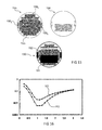
- the figure 16 illustrates a comparison of the mean squared error between a source image and its representation in the form of elementary patterns, in the case of archiving according to the prior art and in the case of archiving according to the invention.
- a source image is compared with the image obtained after optical detection of its representation in the form of elementary patterns.
- the optical detection is that described with reference to the figure 3 , using an optics that introduces an optical blur comparable to a Gaussian spot of width wg. It is an optical detection by Gaussian convolution.
- the abscissa axis corresponds to the width wg of the Gaussian relative to the size of the cell.
- the y-axis corresponds to the mean squared error relative to the source image.
- the source image is a pattern of gray scale tones made up of 20x20 different gray tones randomly distributed spatially and dynamically from 0 to 255.
- the zones have an extension of 3x3 pixels, ie an image to code of 60x60 pixels.
- Curve 161 corresponds to an archiving method according to the prior art using a single layer of platinum oxide 45 nm thick and an amplitude modulation screening using circular openings in opaque cells.
- the pitch of the addressing grid is 0.02 ⁇ m.
- a square cell with side ⁇ equal to 2 ⁇ m is used (see figure 8 ).
- the minimum error is about 2%.
- Curve 162 corresponds to an archiving method according to the invention using two layers of platinum oxide with thicknesses of 45 nm and 30 nm, and amplitude modulation screening using circular openings in cells. opaque.
- the pitch of the addressing grid is 0.02 ⁇ m and a square cell with a side ⁇ equal to 2 ⁇ m is used.
- the minimum error is about 0.6%, about 3 times less than the error obtained with the method according to the prior art and under similar conditions.
- the invention is not limited to the described embodiments.
Landscapes
- Physics & Mathematics (AREA)
- General Physics & Mathematics (AREA)
- Engineering & Computer Science (AREA)
- Manufacturing & Machinery (AREA)
- Exposure And Positioning Against Photoresist Photosensitive Materials (AREA)
Applications Claiming Priority (1)
| Application Number | Priority Date | Filing Date | Title |
|---|---|---|---|
| FR1359398A FR3011347A1 (fr) | 2013-09-30 | 2013-09-30 | Procede d'inscription d'une image et support associe. |
Publications (2)
| Publication Number | Publication Date |
|---|---|
| EP2874005A2 true EP2874005A2 (de) | 2015-05-20 |
| EP2874005A3 EP2874005A3 (de) | 2015-06-03 |
Family
ID=50137746
Family Applications (1)
| Application Number | Title | Priority Date | Filing Date |
|---|---|---|---|
| EP14186497.5A Withdrawn EP2874005A3 (de) | 2013-09-30 | 2014-09-26 | Verfahren zum Aufbringen eines Bildes, und entsprechende Unterlage |
Country Status (3)
| Country | Link |
|---|---|
| US (1) | US20150093706A1 (de) |
| EP (1) | EP2874005A3 (de) |
| FR (1) | FR3011347A1 (de) |
Citations (1)
| Publication number | Priority date | Publication date | Assignee | Title |
|---|---|---|---|---|
| EP2105921A1 (de) | 2008-03-28 | 2009-09-30 | Commissariat a L'Energie Atomique | Bildspeicherverfahren und entsprechender Datenträger für die Speicherung der Bilder |
Family Cites Families (3)
| Publication number | Priority date | Publication date | Assignee | Title |
|---|---|---|---|---|
| US4090031A (en) * | 1974-10-21 | 1978-05-16 | Eli S. Jacobs | Multi-layered opitcal data records and playback apparatus |
| US5278816A (en) * | 1989-09-22 | 1994-01-11 | Russell James T | Recording/reproducing system using wavelength/depth selective optical storage medium |
| US5471455A (en) * | 1994-05-17 | 1995-11-28 | Jabr; Salim N. | High density optical storage system |
-
2013
- 2013-09-30 FR FR1359398A patent/FR3011347A1/fr not_active Withdrawn
-
2014
- 2014-09-25 US US14/496,332 patent/US20150093706A1/en not_active Abandoned
- 2014-09-26 EP EP14186497.5A patent/EP2874005A3/de not_active Withdrawn
Patent Citations (1)
| Publication number | Priority date | Publication date | Assignee | Title |
|---|---|---|---|---|
| EP2105921A1 (de) | 2008-03-28 | 2009-09-30 | Commissariat a L'Energie Atomique | Bildspeicherverfahren und entsprechender Datenträger für die Speicherung der Bilder |
Also Published As
| Publication number | Publication date |
|---|---|
| FR3011347A1 (fr) | 2015-04-03 |
| US20150093706A1 (en) | 2015-04-02 |
| EP2874005A3 (de) | 2015-06-03 |
Similar Documents
| Publication | Publication Date | Title |
|---|---|---|
| EP3129238B1 (de) | Optische sicherheitskomponente mit reflektierender wirkung, herstellung solch einer komponente und sicheres dokument mit solch einer komponente | |
| EP2836371B1 (de) | Optisches sicherheitselement, herstellung eines derartigem sicherheitselements und geschütztes produkt mit diesem element | |
| EP3870453B1 (de) | Sicherheitselement für ein wertdokument, verfahren zu seiner herstellung und dieses enthaltendes wertdokument | |
| FR3072053B1 (fr) | Composant optique de securite a effet reflectif, fabrication d'un tel composant et document securise equipe d'un tel composant | |
| FR2983317A1 (fr) | Procede de formation d'un hologramme synthetique dans une image tramee | |
| WO2021105582A1 (fr) | Un document sécurisé avec une image personnalisee formee a partir d'un hologramme metallique et son procede de fabrication | |
| WO2010139794A1 (fr) | Procède de fabrication d'images colorées avec une résolution micronique enfouies dans un support très robuste et très pérenne | |
| WO2012032266A1 (fr) | Hologramme synthetique crypte et procede de lecture d'un tel hologramme | |
| EP3969293B1 (de) | Optische sicherheitskomponente mit plasmonischem effekt, herstellung einer solchen komponente und sicheres dokument mit einer solchen komponente | |
| Jiang et al. | Solvent-free optical recording of structural colours on pre-imprinted photocrosslinkable nanostructures | |
| WO2022112708A1 (fr) | Image personnalisee formee a partir d'une couche metallique et d'un reseau lenticulaire | |
| EP2874005A2 (de) | Verfahren zum Aufbringen eines Bildes, und entsprechende Unterlage | |
| EP3899605B1 (de) | Vorrichtung zur anzeige eines oder mehrerer transitorischer bilder aus dreidimensionalen mikrostrukturen und verwendungen solch einer vorrichtung | |
| EP4366954B1 (de) | Optische sicherheitskomponenten, herstellung solcher komponenten und mit solchen komponenten ausgestattete sicherheitsdokumente | |
| EP4088946B1 (de) | Herstellung eines bilds aus einer holografischen struktur | |
| EP4319987B1 (de) | Optische reflexionssichtbare sicherheitskomponenten, herstellung solcher komponenten und mit solchen komponenten ausgestattete sicherheitsdokumente | |
| EP2085241B1 (de) | Methoden und Mittel zur Erstellung von grafischen Daten sowie ihr Benutzerschutz und entsprechende Lese- und Speicherverfahren | |
| EP4428614B1 (de) | Verfahren zur dimensionierung einer grauskala-lithographiemaske | |
| EP4642653A1 (de) | Optische, im transmissionbereich sichtbare sicherheitskomponenten, herstellung solcher komponenten und mit solchen komponenten ausgestattete sichere objekte | |
| EP4448296A1 (de) | Sicherheitsvorrichtung zur erzeugung eines vergrösserten projektionsbildes mit mikrolinsen und einer perforierten metallschicht |
Legal Events
| Date | Code | Title | Description |
|---|---|---|---|
| PUAL | Search report despatched |
Free format text: ORIGINAL CODE: 0009013 |
|
| PUAI | Public reference made under article 153(3) epc to a published international application that has entered the european phase |
Free format text: ORIGINAL CODE: 0009012 |
|
| 17P | Request for examination filed |
Effective date: 20140926 |
|
| AK | Designated contracting states |
Kind code of ref document: A2 Designated state(s): AL AT BE BG CH CY CZ DE DK EE ES FI FR GB GR HR HU IE IS IT LI LT LU LV MC MK MT NL NO PL PT RO RS SE SI SK SM TR |
|
| AX | Request for extension of the european patent |
Extension state: BA ME |
|
| AK | Designated contracting states |
Kind code of ref document: A3 Designated state(s): AL AT BE BG CH CY CZ DE DK EE ES FI FR GB GR HR HU IE IS IT LI LT LU LV MC MK MT NL NO PL PT RO RS SE SI SK SM TR |
|
| AX | Request for extension of the european patent |
Extension state: BA ME |
|
| RIC1 | Information provided on ipc code assigned before grant |
Ipc: G03F 7/12 20060101AFI20150424BHEP Ipc: G11B 7/26 20060101ALI20150424BHEP Ipc: G03F 7/20 20060101ALI20150424BHEP |
|
| STAA | Information on the status of an ep patent application or granted ep patent |
Free format text: STATUS: THE APPLICATION IS DEEMED TO BE WITHDRAWN |
|
| 18D | Application deemed to be withdrawn |
Effective date: 20151204 |