EP2884263B1 - Oberflächenverstärktes ramanstreuungselement - Google Patents
Oberflächenverstärktes ramanstreuungselement Download PDFInfo
- Publication number
- EP2884263B1 EP2884263B1 EP13827548.2A EP13827548A EP2884263B1 EP 2884263 B1 EP2884263 B1 EP 2884263B1 EP 13827548 A EP13827548 A EP 13827548A EP 2884263 B1 EP2884263 B1 EP 2884263B1
- Authority
- EP
- European Patent Office
- Prior art keywords
- fine structure
- projections
- raman scattering
- substrate
- molded layer
- Prior art date
- Legal status (The legal status is an assumption and is not a legal conclusion. Google has not performed a legal analysis and makes no representation as to the accuracy of the status listed.)
- Not-in-force
Links
Images




Classifications
-
- G—PHYSICS
- G01—MEASURING; TESTING
- G01N—INVESTIGATING OR ANALYSING MATERIALS BY DETERMINING THEIR CHEMICAL OR PHYSICAL PROPERTIES
- G01N21/00—Investigating or analysing materials by the use of optical means, i.e. using sub-millimetre waves, infrared, visible or ultraviolet light
- G01N21/62—Systems in which the material investigated is excited whereby it emits light or causes a change in wavelength of the incident light
- G01N21/63—Systems in which the material investigated is excited whereby it emits light or causes a change in wavelength of the incident light optically excited
- G01N21/65—Raman scattering
- G01N21/658—Raman scattering enhancement Raman, e.g. surface plasmons
-
- B—PERFORMING OPERATIONS; TRANSPORTING
- B82—NANOTECHNOLOGY
- B82Y—SPECIFIC USES OR APPLICATIONS OF NANOSTRUCTURES; MEASUREMENT OR ANALYSIS OF NANOSTRUCTURES; MANUFACTURE OR TREATMENT OF NANOSTRUCTURES
- B82Y40/00—Manufacture or treatment of nanostructures
-
- G—PHYSICS
- G01—MEASURING; TESTING
- G01N—INVESTIGATING OR ANALYSING MATERIALS BY DETERMINING THEIR CHEMICAL OR PHYSICAL PROPERTIES
- G01N2201/00—Features of devices classified in G01N21/00
- G01N2201/06—Illumination; Optics
- G01N2201/061—Sources
Definitions
- the present invention relates to a surface-enhanced Raman scattering element.
- Known as an example of the above-mentioned minute metal structure is one manufactured by etching a fluorine-containing silica glass layer and a silica glass film which are sequentially stacked on a silicon substrate, so as to form a plurality of minute projections, and then forming a metal film by sputtering (see, for example, Patent Literature 2).
- WO 2010/104520 A1 discloses a broad band structure for surface enhanced Raman spectroscopy.
- the structure is made up of a metal layer and a dielectric layer on the metal layer, wherein the dielectric layer has a controlled thickness that varies from at least one portion of the dielectric layer to at least another portion of the dielectric layer.
- Nanostructures are provided on the dielectric layer, the nanostructures thus being configured to exhibit variable plasmon resonances.
- Non Patent Literature 1 " Q-SERSTM G1 Substrate", [online], Opto Science, Inc., [retrieved on 2012-07-19]. Retrieved from the Internet: ⁇ URL: http://www.optoscience.com/maker/nanova/pdf/Q-SERS_G1.pdf> .
- the invention is defined by the independent claim, which relates to a surface-enhanced Raman scattering element.
- This surface-enhanced Raman scattering element comprises a substrate having a principal surface; a molded layer having a support part formed on the principal surface of the substrate so as to extend along the principal surface and a fine structure part formed on the support part; and a conductor layer formed on the fine structure part and constituting an optical functional part for generating surface-enhanced Raman scattering; the fine structure part including a plurality of projections formed integrally with the support part, the projections being arranged into a two-dimensional array on the support part; the molded layer being relatively thinner in a direction intersecting the principal surface of the substrate at the projections in a center part of a fine structure area formed with the fine structure part in the molded layer than at the projections in an outer edge part of the fine structure area.
- the molded layer has the fine structure part, on which the conductor layer is formed, so as to construct the optical function part for generating surface-enhanced Raman scattering.
- the molded layer is made relatively thin at the center part of the fine structure area formed with the fine structure part and relatively thick at its outer edge part, respectively. This reduces the amount of deformation caused by thermal expansion at the center part mainly contributing to surface-enhanced Raman scattering in the fine structure area and mitigates distortions occurring at the outer edge part of the fine structure area due to its difference in coefficient of thermal expansion from the substrate. Therefore, this surface-enhanced Raman scattering element can stabilize surface-enhanced Raman scattering characteristics.
- the projections have a forming density relatively lower at the outer edge part of the fine structure area than at the center part thereof. This makes it possible to form the molded layer easily and securely by nanoimprinting, for example, such that it becomes relatively thinner at the center part of the fine structure area than at the outer edge part thereof.
- the forming density of the projections is defined by the total volume of the projections formed within a predetermined reference area, for example. Therefore, the forming density herein becomes higher and lower when the total volume of the projections formed within the predetermined area is larger and smaller, respectively.
- the projections to be compared with each other in terms of forming density have a uniform shape, for example, whether the forming density is high or low corresponds to whether the number of projections formed within the predetermined area is large or small.
- the molded layer is made relatively thinner in the direction intersecting the principal surface of the substrate at the center part of the fine structure area than at the outer edge part of the fine structure area due to a gradient in thickness of the support part.
- This can also form the molded layer easily and securely by nanoimprinting, for example, such that it becomes relatively thinner at the center part of the fine structure area than at the outer edge part thereof.
- the surface-enhanced Raman scattering element in accordance with one aspect of the present invention may further comprise a frame part formed on the principal surface of the substrate so as to surround the support part and fine structure part along the principal surface of the substrate. This can make the frame part protect the fine structure part, so as to improve reliability.
- the fine structure part may be formed all over the principal surface of the substrate. This makes it possible to generate surface-enhanced Raman scattering all over the principal surface of the substrate.
- One aspect of the present invention can provide a surface-enhanced Raman scattering element which can stabilize surface-enhanced Raman scattering characteristics.
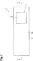
- Fig. 1 is a plan view of the surface-enhanced Raman scattering unit in accordance with an embodiment
- Fig. 2 is a sectional view taken along the line II-II of Fig. 1
- a SERS unit (surface-enhanced Raman scattering unit) 1 in accordance with this embodiment comprises a handling board 2 and a SERS element (surface-enhanced Raman scattering element) 3 attached onto the handling board 2.
- the handling board 2 is a rectangular plate-shaped glass slide, resin board, ceramic board, or the like.
- the SERS element 3 is arranged on a front face 2a of the handling board 2 while being biased to one side in the longitudinal direction of the handling board 2.
- the SERS element 3 comprises a substrate 4 attached onto the handling board 2, a molded layer 5 formed on a front face (principal surface) 4a of the substrate 4, and a conductor layer 6 formed on the molded layer 5.
- the substrate 4 is formed into a rectangular plate by silicon, glass, or the like and has an outer form on the order of several hundred ⁇ m ⁇ several hundred ⁇ m to several ten mm ⁇ several ten mm and a thickness on the order of 100 ⁇ m to 2 mm.
- a rear face 4b of the substrate 4 is secured to the front face 2a of the handling board 2 by direct bonding, bonding with a metal such as solder, eutectic bonding, fusion bonding by irradiation with laser light and the like, anodic bonding, or bonding with a resin.
- a metal such as solder, eutectic bonding, fusion bonding by irradiation with laser light and the like, anodic bonding, or bonding with a resin.
- Fig. 3 is a schematic enlarged sectional view of a region AR in Fig. 2 .
- Fig. 3 omits the conductor layer 6.
- the molded layer 5 has a support part 7 formed on the front face 4a of the substrate 4 and a fine structure part 8 formed on the support part 7.
- the support part 7 is formed so as to extend all over the front face 4a of the substrate 4.
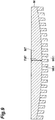
- the support 7 has a thickness T7 with such a gradient as to decrease gradually from an outer edge part 7a of the support part 7 to a center part 7b thereof.
- the thickness T7 of the support part 7 is relatively smaller at the center part 7b than at the outer edge part 7a.
- the thickness T7 of the support part 7 is about 200 nm at the outer edge part 7a and about 100 nm at the center part 7b, for example.
- the fine structure part 8 is formed on the support 7 all over the front face 4a of the substrate 4.
- the fine structure part 8 is formed integrally with the support part 7.
- the molded layer 5 includes a fine structure area A5 formed with the fine structure part 8.
- the fine structure area A5 is also an area extending all over the front face 4a of the substrate 4.
- the support part 7 is also formed all over the front surface 4a of the substrate 4, the fine structure area A5 has an outer edge part 5a and a center part 5b which coincide with the outer edge part 7a and center part 7b of the support part 7, respectively.
- the fine structure part 8 includes a plurality of projections 81 formed on the support 7.
- the projections 81 project from the support part 7 and are formed integrally with the support part 7.
- the projections 81 are arranged into a two-dimensional array on the support part 7 (i.e., on the front face 4a of the substrate 4). A surface 7s of the support part 7 is exposed between the projections 81 adjacent to each other.
- Each projection 81 is formed into a circular column, for example.
- the projections 81 may be arranged into a matrix, a triangle, a honeycomb, or the like.
- the form of the projection 81 is not limited to the circular column but may be any of columns, examples of which include elliptical columns and polygonal columns such as quadrangular columns, or any of cones.
- the forming density of the projections 81 is relatively lower at the outer edge part 5a of the fine structure area A5 than at the center part 5b thereof. That is, the fine structure part 8 has a low-density region 8a which is a ring-shaped region including the outer edge part 5a of the fine structure area A5 and exhibiting a relatively low forming density of the projections 81 and a high-density region 8b which is a region surrounded by the low-density region 8a so as to include the center part 5b of the fine structure area A5 while exhibiting a relatively high forming density of the projections 81.
- a low-density region 8a which is a ring-shaped region including the outer edge part 5a of the fine structure area A5 and exhibiting a relatively low forming density of the projections 81
- a high-density region 8b which is a region surrounded by the low-density region 8a so as to include the center part 5b of the fine structure area A5 while exhibiting
- the forming density of the projections 81 is defined by the total volume of the projections 81 formed within a predetermined reference area R, for example. Therefore, the forming density herein becomes higher and lower when the total volume of the projections 81 formed within the predetermined area R is larger and smaller, respectively. Since the projections 81 to be compared with each other in terms of forming density have a uniform shape here, whether the forming density is high or low corresponds to whether the number of projections 81 formed within the predetermined area R is large or small.
- the projections 81 are formed with a column diameter of about 150 nm, for example.
- the pitch of the projections 81 in the low-density region 8a is about 450 nm, for example.
- the pitch of the projections 81 in the high-density region 8b is smaller than that in the low-density region 8a.
- the projections 81 have a height H81, an example of which is about 180 nm, which is substantially constant in the low-density region 8a and high-density region 8b. That is, the fine structure part 8 has a thickness T8 which is substantially constant all over the fine structure area A5.
- the total thickness T5 of the molded layer 5 has a gradient corresponding to the thickness T7 of the support part 7. More specifically, due to the gradient in the thickness T7 of the support part 7, the thickness T5 of the molded layer 5 is relatively smaller at the center part 5b of the fine structure area A5 than at the outer edge part 5a thereof. In other words, the thickness T5 of the molded layer 5 has such a gradient as to become smaller gradually from the outer edge part 5a of the fine structure area A5 to the center part 5b thereof according to the gradient in the thickness T7 of the support part 7.
- the foregoing molded layer 5 is integrally formed by molding a resin (examples of which include resins based on acrylics, fluorine, epoxy, silicone, and urethane, PET, polycarbonate, and inorganic/organic hybrid materials) or low-melting glass arranged on the front face 4a of the substrate 4 by nanoimprinting, for example.
- a resin examples of which include resins based on acrylics, fluorine, epoxy, silicone, and urethane, PET, polycarbonate, and inorganic/organic hybrid materials
- low-melting glass arranged on the front face 4a of the substrate 4 by nanoimprinting, for example.
- the conductor layer 6 is formed on the fine structure part 8.
- the conductor layer 6 reaches not only the surfaces of the projections 81 but also the surface 7s of the support part 7 exposed between the projections 81. Therefore, the conductor layer 6 has a fine structure corresponding to the fine structure part 8 of the molded layer 5.
- the conductor layer 6 has a thickness on the order of several nm to several ⁇ m, for example.
- the conductor layer 6 like this is formed by vapor-depositing a conductor such as a metal (Au, Ag, Al, Cu, Pt, or the like) on the molded layer 5 molded by nanoimprinting, for example, as mentioned above.
- a conductor such as a metal (Au, Ag, Al, Cu, Pt, or the like)
- the conductor layer 6 formed on the fine structure part 8 and the surface 7a of the support part 7 constructs an optical function part 10 which generates surface-enhanced Raman scattering.
- the SERS unit 1 is prepared. Subsequently, a sample of a solution (or a dispersion of a powder sample in a solution such as water or ethanol; the same hereinafter) is dropped with a pipette or the like, so as to be arranged on the optical function part 10. The sample is arranged on the conductor layer 6, which is formed on the surface 7s of the support part 7 and the surfaces of the projections 81 of the fine structure part 8.
- a spacer made of silicone or the like may be arranged beforehand on the handling board 2 in order to form a sample cell.
- a glass cover is mounted on the optical function part 10 (or can be mounted on a spacer when the spacer is used) and brought into close contact with the solution sample.
- the SERS unit 1 is set in a Raman spectroscopic analyzer, and the sample arranged on the optical function part 10 is irradiated with excitation light through the glass cover.
- This generates surface-enhanced Raman scattering at the interface between the optical function part 10 and sample, whereby surface-enhanced Raman scattering light derived from the sample is enhanced by about 10 8 times, for example, and released.
- the Raman spectroscopic analyzer enables Raman spectroscopy with high sensitivity and high accuracy.
- the following methods may also be used for arranging the sample on the optical function part 10.
- the SERS element 3 may be dipped in and lifted from the solution sample, and then the sample may be blown to dry. A minute amount of the solution sample may be dropped onto the optical function part 10 and left to dry. A powder sample may be dispersed as it is on the optical function part 10.
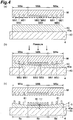
- a mold M is prepared in this manufacturing method.
- the mold M has a pattern which is the reverse of the above-mentioned fine structure part 8 of the molded layer 5. More specifically, the mold M has a high-density region M8a at an outer edge part formed with projections M81 having a relatively large column diameter and a low-density region M8b at a center part formed with projections M82 having a relatively small column diameter.
- a depression M83 defined by the projections M81, M82 adjacent to each other corresponds to the projection 81 in the molded layer 5. Since the projections 81 in the molded layer 5 have a fixed column diameter D81, the depressions M83 in the mold M have a fixed width. Therefore, in the high-density region M8a of the mold M formed with the relatively large projections M81, the depressions M83 have a wider gap therebetween and a relatively small total volume. In the low-density region M8b of the mold M formed with the relatively small projections M82, by contrast, the depressions M83 have a narrower gap therebetween and a relatively large total volume.
- the mold M may be either a master mold for nanoimprinting or a replica mold formed by using the master mold.
- the mold M may be either a film mold made of PET, polycarbonate, PMMA, polyimide, silicone, or the like, or a silica mold, a nickel mold, a silicon mold, or the like without being restricted to film molds, for example.
- a wafer 40 including the substrate 4 is prepared, and a nanoimprinting resin 50 is arranged on its surface 40a.
- a UV-curable resin (examples of which include resins based on acrylics, fluorine, epoxy, silicone, and urethane, PET, polycarbonate, and inorganic/organic hybrid materials) or low-melting glass can be used, for example.
- each of the depressions M83 of the mold M is filled with the nanoimprinting resin 50 (though there is a case where it is not fully filled).
- the depressions M83 in the high-density region M8a of the mold M where the total volume of the depressions M83 is relatively small can be filled with a smaller amount of resin.
- a relatively large amount of resin is necessary for filling the depressions M83 in the low-density region M8b of the mold M where the total volume of the depressions M83 is relatively large.
- the molded layer 5 is formed by transferring the pattern of the mold M to the nanoimprinting resin 50 under such a circumstance, relatively small and large amounts of resin are required to fill the depressions M83 in the high-density region M8a and low-density region M8b, respectively, at the time of pressing the mold M against the nanoimprinting resin 50, whereby a gradient is generated in the amount of resin utilized for forming the support part 7 so as to correspond to these regions M8a, M8b, which results in the above-mentioned gradient in thickness of the support part 7.
- the nanoimprinting resin 50 is cured by UV irradiation, for example, and the mold M is released from the molded layer 5 as illustrated in (c) of Fig. 4 .
- the low-density region 8a and high-density region 8b in the fine structure part 8 can easily and securely form the molded layer 5 (support part 7) having a gradient in thickness because of the fact that the amount of resin required for forming the depressions 81 in the high-density region 8b (the amount of resin for filling the depressions M83 in the low-density region M8b of the mold M) is greater than the amount of resin required for forming the depressions 81 in the low-density region 8a (the amount of resin for filling the depressions M83 in the high-density region M8a of the mold M).
- the nanoimprinting process illustrated in (a) to (c) of Fig. 4 may be performed such as to form a plurality of molded layers 5 collectively on a wafer level by using the mold M in a wafer size, or a plurality of molded layers 5 may be formed sequentially by repeatedly using the mold M having a size smaller than that of the wafer (step & repeat).
- a conductor such as a metal (Au, Ag, Al, Cu, Pt, or the like) is vapor-deposited on the molded layer 5 (fine structure part 8), so as to form the conductor layer 6, thereby constituting the optical function part 10.
- a conductor such as a metal (Au, Ag, Al, Cu, Pt, or the like) is vapor-deposited on the molded layer 5 (fine structure part 8), so as to form the conductor layer 6, thereby constituting the optical function part 10.
- the wafer 40 is diced into the SERS elements 3, and the cut SERS element 3 is secured to the handling board 2, whereby the SERS unit 1 is obtained.
- the molded layer 5 has the fine structure part 8, on which the conductor layer 6 is formed, so as to construct the optical function part 10 for generating surface-enhanced Raman scattering.
- the thickness T5 of the molded layer 5 is constructed relatively large at the outer edge part 5a of the fine structure area A5 formed with the fine structure part 8 but relatively small at the center part 5b. This reduces the amount of deformation caused by thermal expansion at the center part 5b mainly contributing to surface-enhanced Raman scattering and mitigates distortions occurring at the outer edge part 5a due to its difference in coefficient of thermal expansion from the substrate 4. Therefore, this SERS element 3 can stabilize surface-enhanced Raman scattering characteristics.
- the above-mentioned structure concerning the thickness T5 of the molded layer 5 in the SERS element 3 is achieved according to the inventors' finding that, since the expansion of a resin or the like is obtained by multiplying its thickness, the coefficient of thermal expansion, and the change in temperature, the advantageous effects mentioned above can be attained when the thickness T5 of the molded layer 5 is made larger at the outer edge part 5a, which is allowed to deform, so as to mitigate distortions occurring due to its difference in coefficient of thermal expansion from the substrate 4, while making the thickness T5 of the molded layer 5 smaller at the center part 5b to be restrained from deforming, so as to reduce the absolute amount of expansion caused by thermal expansion.
- the fine structure part 8 includes a plurality of projections 81, while the forming density of the projections 81 is relatively lower at the outer edge part 5a of the fine structure area A5 than at the center part 5b thereof.
- the molded layer 5 like this can be formed easily and securely such that its thickness T5 is relatively smaller at the center part 5b of the fine structure area A5 than at the outer edge part 5a thereof by nanoimprinting using the above-mentioned mold M, for example. The same also applies when providing the thickness T7 of the support part 7 with the above-mentioned gradient.
- the molded layer 5 has the support part 7 extending along the front face 4a of the substrate 4, while the fine structure part 8 (projection 81) is constructed integrally with the support part 7. This restrains the fine structure part 8 from peeling (the projections 81 from falling and dropping) and thus improves reliability.
- the thickness T5 of the molded layer 5 decreases gradually from the outer edge part 5a of the fine structure area A5 to the center part 5b thereof, thereby forming a recess as a whole. Therefore, reserving the solution sample in this recess can improve the ratio by which the sample adheres to the fine structure part 8 (i.e., to the conductor layer 6 on the fine structure part 8).
- the present invention is not limited to the above-mentioned SERS element 3, but may encompass any modifications of the SERS element 3 within the scope defined by the independent claim.
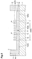
- the SERS element 3 may comprise a molded layer 5A illustrated in Fig. 5 in place of the above-mentioned molded layer 5.
- the molded layer 5A has a fine structure part 8A in place of the fine structure part 8.
- the fine structure part 8A is formed at the center part 7b of the support part 7. More specifically, the fine structure part 8A includes a plurality of projections 81 projecting from the center part 7b of the support part 7. The projections 81 are not formed at the outer edge part 7a of the support 7. Therefore, the fine structure area A5 does not cover all over the front face 4a of the substrate 4 but only the center part thereof.
- the forming density of the projections 81 is constant in the fine structure area A5.
- the thickness T8 of the fine structure part 8A is constant, while the thickness T7 of the support part 7 has a gradient, whereby the thickness T5 of the molded layer 5A has a gradient corresponding to the thickness T7 of the support part 7 in this case as well. More specifically, due to the gradient in the thickness T7 of the support part 7, the thickness T5 of the molded layer 5A is relatively thinner at the center part 5b of the fine structure area A5 than at the outer edge part 5a thereof. In other words, the thickness T5 of the molded layer 5A has such a gradient as to become smaller gradually from the outer edge part 5a of the fine structure area A5 to the center part 5b thereof according to the gradient in the thickness T7 of the support part 7.
- the molded layer 5A further has a frame part 9 formed on the front face 4a of the substrate 4.
- the frame part 9 is continuous from the support part 7 and formed integrally therewith.
- the frame part 9 is arranged at an outer peripheral part of the front face 4a of the substrate 4, is formed like a ring so as to surround the support part 7 and fine structure part 8 along the front face 4a of the substrate 4.
- the frame part 9 has a height H9 from the front face 4a of the substrate 4 greater than the height of the fine structure part 8 from the front face 4a of the substrate 4 (the sum of the thickness T7 of the support part 7 and the thickness T8 of the fine structure part 8). Therefore, in the molded layer 5A, the frame part 9 and support part 7 define a recess C, while the fine structure part 8 (projection 81) is formed on the bottom face of the recess C (the surface 7s of the support part 7).
- the frame part 9 protects the fine structure part 8, thereby improving reliability.
- the recess C can also reserve the solution sample, thereby improving the ratio by which the sample adheres to the fine structure part 8 (i.e., to the conductor layer 6 on the fine structure part 8).
- the solution sample does not leak out of the boundary between the frame part 9 and support part 7, since the frame 9 is formed integrally with the support part 7.
- Raman spectroscopic analysis can be conducted with a glass cover mounted on the frame part 9 and thus can be performed while protecting the fine structure part 8 (blocking impurities from mingling) and preventing the solution from evaporating.
- the distance between the arranged glass cover and the fine structure part 8 can be kept constant among different elements, so as to achieve stable measurement (suppress fluctuations in measurement caused by variations in distance). Arranging a flat glass cover can suppress the lens effect of the solution sample, thereby enabling appropriate measurement.
- the molded layer 5A also reduces the amount of deformation caused by thermal expansion at the center part 5b mainly contributing to surface-enhanced Raman scattering and mitigates distortions occurring at a part including the frame part 9 due to its difference in coefficient of thermal expansion from the substrate 4, thereby making it possible to prevent the molded layer 5A from peeling due to temperature cycles and the like.
- the frame part 9 can also be used as a space for providing an alignment mark for mounting or a space to be marked for identifying chips. Chipping, if any, occurring in the SERS element 3 stops at the frame part 9, thereby avoiding an effective area including the fine structure part 8 from being damaged.
- the foregoing molded layer 5A can be formed by nanoimprinting similar to that forming the molded layer 5 if the mold M is provided with a pattern corresponding to the frame part 9 (a recess) in the above-mentioned manufacturing method.
- the whole structure area A5 formed with the projections 81 as a whole can be regarded as the high-density region 8b, while the outer edge part 7a of the support part 7 not formed with the projections 81 can be regarded as the low-density region 8a, whereby the support part 7 can be formed such that the thickness T7 is relatively smaller at the center part 7b than at the outer edge part 7a.
- the molded layer 5A has the frame part 9 having a volume larger than that of the projections 81, a greater amount of resin is required for forming the frame part 9 (for filling the recess of the mold M corresponding to the frame part 9), whereby the thickness T7 of the support part 7 becomes smaller (the support part 7 is formed with a recess) at the boundary part between the frame part 9 and support part 7.
- Adjusting the forming density of the frame part 9 in a frame region can set the height H9 of the frame part 9 greater than the height of the fine structure part 8 (the sum of the thickness T7 of the support part 7 and the thickness T8 of the fine structure part 8).
- the height H9 of the frame part 9 from the front face 4a of the substrate 4 may be made smaller than the height of the fine structure part 8A from the front face 4a of the substrate 4 (the sum of the thickness T7 of the support part 7 and the thickness T8 of the fine structure part 8A), so as to become substantially the same as the height of the support part 7 (thickness T7) from the front face 4a of the substrate 4.
- the frame part 9 is relatively lower (thinner) than the fine structure part 8A and thus can be utilized as a region for setting a cut line for chipping and also is less likely to peel during dicing for chipping.
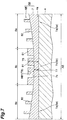
- the SERS element 3 may comprise a molded layer 5B illustrated in Fig. 7 in place of the molded layer 5.
- the molded layer 5B has a fine structure part 8B instead of the fine structure part 8.
- the fine structure part 8B is formed all over the front face 4a of the substrate 4, whereby the fine structure area A5 extends all over the front face 4a of the substrate 4.
- the fine structure part 8B has a plurality of projections 81, 82 projecting from the support part 7.
- the projections 81 have a column diameter larger than that of the projections 82 and are formed at the center part 5b of the fine structure area A5.
- the projections 82 are formed at the outer edge part 5a of the fine structure area A5.
- the space between the projections 81 adjacent to each other is smaller than that between the projections 82 adjacent to each other. Therefore, the forming density of the projections 81 is higher than that of the projections 82.
- the fine structure part 8B has a low-density region 8a which is a ring-shaped region including the outer edge part 5a of the fine structure area A5 and exhibiting a relatively low forming density of the projections 82 and a high-density region 8b which is a region surrounded by the low-density region 8a so as to include the center part 5b of the fine structure area A5 while exhibiting a relatively high forming density of the projections 81.
- the total thickness T5 of the molded layer 5B also has a gradient corresponding to the thickness T7 of the support part 7. More specifically, due to the gradient in the thickness T7 of the support part 7, the thickness T5 of the molded layer 5B is relatively thinner at the center part 5b of the fine structure area A5 than at the outer edge part 5a thereof. In other words, the thickness T5 of the molded layer 5B has such a gradient as to become smaller gradually from the outer edge part 5a of the fine structure area A5 to the center part 5b thereof according to the gradient in the thickness T7 of the support part 7.
- the form (column diameter) of projections may vary between the low-density region 8a and high-density region 8b of the fine structure part 8B.
- Preparing the mold M for the molded layer 5B and pressing it against the nanoimprinting resin 50 can provide the support part 7 with a gradient due to the fact that a larger amount of resin is necessary for forming the projections 81 than the projections 82 in this case as well.
- the molded layer 5 includes the fine structure part 8 having the low-density region 8a and high-density region 8b whose forming densities of the projections 81 differ from each other, so that the thickness T5 of the molded layer 5 (the thickness T7 of the support part 7) is provided with a gradient due to whether the forming density of the projections 81 is high or low (due to whether the required amount of resin is large or small), when forming the molded layer 5 by nanoimprinting in the above-mentioned embodiment, but the method for providing the thickness T5 of the molded layer 5 with a gradient is not limited thereto.
- the thickness T5 of the molded layer 5C (i.e., the thickness T7 of the support part 7) can be provided with such a gradient as to become smaller gradually from the outer edge part 5a of the fine structure area A5 to the center part 5b by similar nanoimprinting if the mold M used for forming this layer has a thickness TM7 of a support part M7 provided with a corresponding gradient beforehand as illustrated in Fig. 9 .
- the molded layer in the SERS element 3 is only required to be relatively thinner at the center part 5b of the fine structure area A5 formed with the fine structure part 8 than at the outer edge part 5a thereof, but may become thinner stepwise (e.g., in two or three steps) from the outer edge part 5a to the center part 5b and need not be formed by nanoimprinting.
- the forming density of the projections 81 in the fine structure part 8 has two stages of high and low densities in the molded layer 5
- the forming density of the projections 81 is only required to be relatively lower at the outer edge part 5a of the fine structure area A5 than at the center part 5b thereof and may be provided with three or more stages of forming density differences.
- the conductor layer 6 is not limited to the one directly formed on the molded layer 5 (fine structure part 8), but may be formed indirectly on the molded layer 5 (fine structure part 8) with a layer such as a buffer metal (Ti, Cr, or the like) for improving the adhesion of a metal to the molded layer 5 (fine structure part 8), for example, interposed therebetween.
- a buffer metal Ti, Cr, or the like
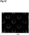
- the optical function part shown in Fig. 10 is one in which Au was vapor-deposited as a conductor layer so as to yield a thickness of 50 nm in a fine structure part made of a nanoimprinting resin having a plurality of pillars (each having a diameter of 120 nm and a height of 180 nm) periodically arranged at a predetermined pitch (center line distance of 360 nm).
- One aspect of the present invention can provide a surface-enhanced Raman scattering element which can stabilize surface-enhanced Raman scattering characteristics.
- SERS unit surface-enhanced Raman scattering unit
- 3 SERS element (surface-enhanced Raman scattering element);
- 4 substrate; 4a: front face (principal surface);
- 5 molded layer; 5a: outer edge part; 5b: center part; 6: conductor layer; 7: support part; 8: fine structure part; 9: frame part; 10: optical function part; 81: projection;
- A5 fine structure area.
Landscapes
- Health & Medical Sciences (AREA)
- Nuclear Medicine, Radiotherapy & Molecular Imaging (AREA)
- Physics & Mathematics (AREA)
- Life Sciences & Earth Sciences (AREA)
- Chemical & Material Sciences (AREA)
- Analytical Chemistry (AREA)
- Biochemistry (AREA)
- General Health & Medical Sciences (AREA)
- General Physics & Mathematics (AREA)
- Immunology (AREA)
- Pathology (AREA)
- Investigating, Analyzing Materials By Fluorescence Or Luminescence (AREA)
Claims (4)
- Oberflächenverstärktes Ramanstreuungselement (3), umfassend:ein Substrat (4), das eine Hauptoberfläche (4a) aufweist;eine geformte Schicht (5), die ein Stützteil (7) aufweist, das auf der Hauptoberfläche (4a) des Substrats (4) gebildet ist, um sich entlang der Hauptoberfläche (4a) zu erstrecken, und ein Feinstrukturteil (8), das auf dem Stützteil (7) gebildet ist; undeine Leiterschicht (6), die auf dem Feinstrukturteil (8) gebildet ist und ein optisches Funktionsteil (10) zum Generieren von oberflächenverstärkter Ramanstreuung ausbildet;dadurch gekennzeichnet, dass das Feinstrukturteil (8) eine Vielzahl von Vorsprüngen (81) beinhaltet, die integral mit dem Stützteil (7) gebildet sind,wobei die Vorsprünge (81) in einem zweidimensionalen Array auf dem Stützteil (7) angeordnet sind,wobei die geformte Schicht (5) in einer Richtung, die die Hauptoberfläche (4a) des Substrats (4) schneidet, an den Vorsprüngen in einem mittleren Teil eines Feinstrukturbereichs (A5), der mit dem Feinstrukturteil (8) in der geformten Schicht (5) gebildet ist, relativ dünner ist als an den Vorsprüngen in einem Außenkantenteil des Feinstrukturbereichs (A5),wobei die geformte Schicht (5) in der Richtung, die die Hauptoberfläche (4a) des Substrats (4) schneidet, in dem mittleren Teil des Feinstrukturbereichs (A5) relativ dünner gefertigt ist als an dem Außenkantenteil des Feinstrukturbereichs (A5) aufgrund eines Dicke-Gradienten des Stützteils (7).
- Oberflächenverstärktes Ramanstreuungselement (3) nach Anspruch 1, wobei die Vorsprünge (81) eine relativ niedrigere Bildungsdichte an dem Außenkantenteil des Feinstrukturbereichs (A5) aufweisen als in dem mittleren Teil davon.
- Oberflächenverstärktes Ramanstreuungselement (3) nach Anspruch 1 oder 2, weiter umfassend ein Rahmenteil (9), das auf der Hauptoberfläche (4a) des Substrats (4) gebildet ist, um das Stützteil (7) und das Feinstrukturteil (8) entlang der Hauptoberfläche (4a) des Substrats zu umgeben.
- Oberflächenverstärktes Ramanstreuungselement (3) nach Anspruch 1 oder 2, wobei das Feinstrukturteil (8) über die gesamte Hauptoberfläche (4a) des Substrats (4) gebildet ist.
Applications Claiming Priority (2)
| Application Number | Priority Date | Filing Date | Title |
|---|---|---|---|
| JP2012178768A JP5921380B2 (ja) | 2012-08-10 | 2012-08-10 | 表面増強ラマン散乱ユニット |
| PCT/JP2013/071700 WO2014025031A1 (ja) | 2012-08-10 | 2013-08-09 | 表面増強ラマン散乱素子 |
Publications (3)
| Publication Number | Publication Date |
|---|---|
| EP2884263A1 EP2884263A1 (de) | 2015-06-17 |
| EP2884263A4 EP2884263A4 (de) | 2016-08-10 |
| EP2884263B1 true EP2884263B1 (de) | 2020-10-28 |
Family
ID=50068247
Family Applications (1)
| Application Number | Title | Priority Date | Filing Date |
|---|---|---|---|
| EP13827548.2A Not-in-force EP2884263B1 (de) | 2012-08-10 | 2013-08-09 | Oberflächenverstärktes ramanstreuungselement |
Country Status (5)
| Country | Link |
|---|---|
| US (1) | US9726608B2 (de) |
| EP (1) | EP2884263B1 (de) |
| JP (1) | JP5921380B2 (de) |
| CN (1) | CN104520695B (de) |
| WO (1) | WO2014025031A1 (de) |
Families Citing this family (4)
| Publication number | Priority date | Publication date | Assignee | Title |
|---|---|---|---|---|
| JP6294797B2 (ja) * | 2014-09-10 | 2018-03-14 | 浜松ホトニクス株式会社 | 表面増強ラマン散乱ユニット |
| CN107075661B (zh) * | 2014-09-26 | 2020-03-17 | 韩国机械研究院 | 形成有多个纳米间隙的基底及其制备方法 |
| JP6607635B2 (ja) * | 2015-09-09 | 2019-11-20 | 学校法人 東洋大学 | 測定用器具 |
| US11067507B2 (en) * | 2017-06-01 | 2021-07-20 | Versitech Limited | Sensors with gradient nanostructures and associated method of use |
Family Cites Families (57)
| Publication number | Priority date | Publication date | Assignee | Title |
|---|---|---|---|---|
| JPH0544867U (ja) | 1991-11-18 | 1993-06-15 | 三洋電機株式会社 | 測定装置の包装体 |
| JPH07260646A (ja) | 1994-03-17 | 1995-10-13 | Nikon Corp | 試料容器 |
| US6242264B1 (en) | 1996-09-04 | 2001-06-05 | The Penn State Research Foundation | Self-assembled metal colloid monolayers having size and density gradients |
| US20040023046A1 (en) | 1998-08-04 | 2004-02-05 | Falko Schlottig | Carrier substrate for Raman spectrometric analysis |
| JP2003026232A (ja) | 2001-07-18 | 2003-01-29 | Seiko Epson Corp | 梱包方法及び緩衝材 |
| US7460224B2 (en) | 2005-12-19 | 2008-12-02 | Opto Trace Technologies, Inc. | Arrays of nano structures for surface-enhanced Raman scattering |
| CN100357738C (zh) | 2004-03-26 | 2007-12-26 | 博奥生物有限公司 | 一种检测小分子化合物的方法 |
| RU2361193C2 (ru) | 2004-05-19 | 2009-07-10 | Вп Холдинг, Ллс | Оптический датчик с многослойной плазмонной структурой для усовершенствованного обнаружения химических групп посредством sers |
| JP2005337771A (ja) * | 2004-05-25 | 2005-12-08 | National Institute For Materials Science | ナノ構造を有する集積化ピラー構造光学素子 |
| GB0424458D0 (en) | 2004-11-04 | 2004-12-08 | Mesophotonics Ltd | Metal nano-void photonic crystal for enhanced raman spectroscopy |
| US7245370B2 (en) | 2005-01-06 | 2007-07-17 | Hewlett-Packard Development Company, L.P. | Nanowires for surface-enhanced Raman scattering molecular sensors |
| JP2008026109A (ja) | 2006-07-20 | 2008-02-07 | Fujifilm Corp | 微細構造体及びその製造方法、センサデバイス及びラマン分光用デバイス |
| US7528948B2 (en) | 2006-07-25 | 2009-05-05 | Hewlett-Packard Development Company, L.P. | Controllable surface enhanced Raman spectroscopy |
| WO2008030666A2 (en) * | 2006-07-25 | 2008-03-13 | The Board Of Trustees Of The University Of Illinois | Multispectral plasmonic crystal sensors |
| EP2074421B1 (de) | 2006-10-12 | 2014-12-17 | Koninklijke Philips N.V. | Schneller biosensor mit reagenzschicht |
| US7388661B2 (en) | 2006-10-20 | 2008-06-17 | Hewlett-Packard Development Company, L.P. | Nanoscale structures, systems, and methods for use in nano-enhanced raman spectroscopy (NERS) |
| JP2008128786A (ja) | 2006-11-20 | 2008-06-05 | Canon Inc | 表面増強振動分光分析用治具及びその製造方法 |
| JP2008196992A (ja) | 2007-02-14 | 2008-08-28 | National Institute Of Information & Communication Technology | 表面プラズモンの電場増強構造 |
| JP5397577B2 (ja) | 2007-03-05 | 2014-01-22 | オムロン株式会社 | 表面プラズモン共鳴センサ及び当該センサ用チップ |
| CN101024483B (zh) | 2007-03-27 | 2010-12-29 | 吉林大学 | 金属有序结构表面增强基底的构筑方法 |
| JP2008268059A (ja) | 2007-04-23 | 2008-11-06 | St Japan Inc | 試料ホルダ |
| JP4993360B2 (ja) | 2007-06-08 | 2012-08-08 | 富士フイルム株式会社 | 微細構造体及びその製造方法、光電場増強デバイス |
| JP2009047623A (ja) | 2007-08-22 | 2009-03-05 | Jiyasuko Eng Kk | 透過測定用ホルダ |
| JP2009103643A (ja) | 2007-10-25 | 2009-05-14 | Fujifilm Corp | 表面増強ラマン分光装置 |
| US8115920B2 (en) | 2007-11-14 | 2012-02-14 | 3M Innovative Properties Company | Method of making microarrays |
| JP2009222507A (ja) | 2008-03-14 | 2009-10-01 | National Institute Of Advanced Industrial & Technology | 微量物質検出素子 |
| JP2009236830A (ja) | 2008-03-28 | 2009-10-15 | Sumitomo Precision Prod Co Ltd | 被分析物担体、及び、その製造方法 |
| CN101281133B (zh) | 2008-05-12 | 2010-08-18 | 中国科学院合肥物质科学研究院 | 具有大面积微纳树状结构阵列的表面增强拉曼活性基底的制备方法 |
| CN101629906A (zh) * | 2008-07-20 | 2010-01-20 | 欧普图垂斯科技有限公司 | 检测被测对象中特定化学物质的方法及系统 |
| JP4980324B2 (ja) | 2008-09-30 | 2012-07-18 | テルモ株式会社 | 成分測定装置 |
| JP5042371B2 (ja) | 2008-10-30 | 2012-10-03 | 日本電信電話株式会社 | 測定チップ着脱装置、spr測定システム及び測定チップ着脱方法 |
| CN102282094A (zh) | 2008-11-17 | 2011-12-14 | 惠普开发有限公司 | 用于表面增强拉曼散射(sers)的衬底 |
| JP5632751B2 (ja) | 2009-02-09 | 2014-11-26 | 浜松ホトニクス株式会社 | 加工対象物切断方法 |
| WO2010104520A1 (en) | 2009-03-13 | 2010-09-16 | Hewlett-Packard Development Company, L.P. | Broad band structures for surface enhanced raman spectroscopy |
| EP2419733A4 (de) | 2009-04-13 | 2013-12-25 | Univ Leland Stanford Junior | Verfahren und vorrichtungen zur erkennung des vorhandenseins eines analyts in einer probe |
| JP2011021085A (ja) | 2009-07-15 | 2011-02-03 | Yokohama Rubber Co Ltd:The | 空気入りタイヤ用ゴム組成物 |
| JP2011033518A (ja) | 2009-08-04 | 2011-02-17 | Toray Res Center:Kk | 表面増強ラマン分光分析方法 |
| US8659391B2 (en) | 2009-08-18 | 2014-02-25 | Indian Institute Of Technology Madras | Multielement and multiproperty tagging |
| EP2478343A1 (de) | 2009-09-17 | 2012-07-25 | Hewlett-Packard Development Company, L.P. | Elektrisch betriebene vorrichtungen für oberflächenverstärkte raman-spektroskopie |
| TWI523950B (zh) | 2009-09-30 | 2016-03-01 | 凸版印刷股份有限公司 | 核酸分析裝置 |
| JP2011075348A (ja) | 2009-09-30 | 2011-04-14 | Nidek Co Ltd | 試験片の製造方法 |
| WO2011047690A1 (en) | 2009-10-23 | 2011-04-28 | Danmarks Tekniske Universitet | Surface enhanced raman scattering substrates consumables for raman spectroscopy |
| US8415611B2 (en) * | 2009-11-19 | 2013-04-09 | Seiko Epson Corporation | Sensor chip, sensor cartridge, and analysis apparatus |
| JP5544836B2 (ja) | 2009-11-19 | 2014-07-09 | オムロン株式会社 | 表面プラズモン共鳴チップ |
| US20110166045A1 (en) * | 2009-12-01 | 2011-07-07 | Anuj Dhawan | Wafer scale plasmonics-active metallic nanostructures and methods of fabricating same |
| JP5589656B2 (ja) * | 2009-12-11 | 2014-09-17 | セイコーエプソン株式会社 | センサーチップ、センサーカートリッジ及び分析装置 |
| JP5574783B2 (ja) | 2010-03-31 | 2014-08-20 | 富士フイルム株式会社 | 蛍光検出装置および方法 |
| JP5560891B2 (ja) | 2010-05-13 | 2014-07-30 | セイコーエプソン株式会社 | 光デバイス及び分析装置 |
| US9182338B2 (en) | 2010-05-21 | 2015-11-10 | The Trustees Of Princeton University | Structures for enhancement of local electric field, light absorption, light radiation, material detection and methods for making and using of the same |
| JP5614278B2 (ja) | 2010-12-24 | 2014-10-29 | セイコーエプソン株式会社 | センサーチップ、センサーチップの製造方法、検出装置 |
| JP5779963B2 (ja) | 2011-04-28 | 2015-09-16 | ナノフォトン株式会社 | 観察試料密閉容器 |
| WO2013015810A2 (en) | 2011-07-27 | 2013-01-31 | Hewlett-Packard Development Company, L.P. | Surface enhanced raman spectroscopy employing a nanorod in a surface indentation |
| EP2769214B1 (de) | 2011-10-18 | 2019-05-22 | Hewlett-Packard Development Company, L.P. | Molekulare erfassungsvorrichtung |
| JP5848458B2 (ja) * | 2011-10-27 | 2016-01-27 | ヒューレット−パッカード デベロップメント カンパニー エル.ピー.Hewlett‐Packard Development Company, L.P. | 化学種をフィルタリングする装置 |
| TWI469917B (zh) | 2012-08-09 | 2015-01-21 | Nat Univ Tsing Hua | 具表面增強拉曼散射活性之結構、其製造方法及其偵測裝置 |
| CN108827928B (zh) | 2012-08-10 | 2021-12-24 | 浜松光子学株式会社 | 表面增强拉曼散射单元及其使用方法 |
| EP4033222A1 (de) | 2012-08-10 | 2022-07-27 | Hamamatsu Photonics K.K. | Oberflächenverstärkte ramanstreuungseinheit |
-
2012
- 2012-08-10 JP JP2012178768A patent/JP5921380B2/ja not_active Expired - Fee Related
-
2013
- 2013-08-09 CN CN201380042449.8A patent/CN104520695B/zh not_active Expired - Fee Related
- 2013-08-09 US US14/420,449 patent/US9726608B2/en not_active Expired - Fee Related
- 2013-08-09 WO PCT/JP2013/071700 patent/WO2014025031A1/ja not_active Ceased
- 2013-08-09 EP EP13827548.2A patent/EP2884263B1/de not_active Not-in-force
Non-Patent Citations (1)
| Title |
|---|
| None * |
Also Published As
| Publication number | Publication date |
|---|---|
| WO2014025031A1 (ja) | 2014-02-13 |
| US9726608B2 (en) | 2017-08-08 |
| CN104520695A (zh) | 2015-04-15 |
| JP5921380B2 (ja) | 2016-05-24 |
| CN104520695B (zh) | 2018-04-13 |
| EP2884263A1 (de) | 2015-06-17 |
| EP2884263A4 (de) | 2016-08-10 |
| JP2014037972A (ja) | 2014-02-27 |
| US20150219561A1 (en) | 2015-08-06 |
Similar Documents
| Publication | Publication Date | Title |
|---|---|---|
| US10408761B2 (en) | Surface-enhanced Raman scattering element | |
| US9857306B2 (en) | Surface-enhanced Raman scattering element | |
| JP6571148B2 (ja) | 表面増強ラマン散乱素子の製造方法 | |
| US9874523B2 (en) | Surface-enhanced Raman scattering element including a conductor layer having a base part and a plurality of protusions | |
| US9976961B2 (en) | Surface-enhanced raman scattering element including a conductor layer having a base part and a plurality of protusions | |
| US9846123B2 (en) | Surface-enhanced Raman scattering element | |
| EP4033222A1 (de) | Oberflächenverstärkte ramanstreuungseinheit | |
| EP2884264B1 (de) | Oberflächenverstärktes raman-streuungselement und herstellungsverfahren dafür | |
| EP2884263B1 (de) | Oberflächenverstärktes ramanstreuungselement | |
| US9612201B2 (en) | Surface-enhanced raman scattering element | |
| JP6284610B2 (ja) | 表面増強ラマン散乱ユニット |
Legal Events
| Date | Code | Title | Description |
|---|---|---|---|
| PUAI | Public reference made under article 153(3) epc to a published international application that has entered the european phase |
Free format text: ORIGINAL CODE: 0009012 |
|
| 17P | Request for examination filed |
Effective date: 20150306 |
|
| AK | Designated contracting states |
Kind code of ref document: A1 Designated state(s): AL AT BE BG CH CY CZ DE DK EE ES FI FR GB GR HR HU IE IS IT LI LT LU LV MC MK MT NL NO PL PT RO RS SE SI SK SM TR |
|
| AX | Request for extension of the european patent |
Extension state: BA ME |
|
| DAX | Request for extension of the european patent (deleted) | ||
| RA4 | Supplementary search report drawn up and despatched (corrected) |
Effective date: 20160707 |
|
| RIC1 | Information provided on ipc code assigned before grant |
Ipc: B82Y 15/00 20110101ALI20160701BHEP Ipc: B82Y 40/00 20110101ALI20160701BHEP Ipc: G01N 21/65 20060101AFI20160701BHEP |
|
| STAA | Information on the status of an ep patent application or granted ep patent |
Free format text: STATUS: EXAMINATION IS IN PROGRESS |
|
| 17Q | First examination report despatched |
Effective date: 20191206 |
|
| GRAP | Despatch of communication of intention to grant a patent |
Free format text: ORIGINAL CODE: EPIDOSNIGR1 |
|
| STAA | Information on the status of an ep patent application or granted ep patent |
Free format text: STATUS: GRANT OF PATENT IS INTENDED |
|
| INTG | Intention to grant announced |
Effective date: 20200528 |
|
| GRAS | Grant fee paid |
Free format text: ORIGINAL CODE: EPIDOSNIGR3 |
|
| GRAA | (expected) grant |
Free format text: ORIGINAL CODE: 0009210 |
|
| STAA | Information on the status of an ep patent application or granted ep patent |
Free format text: STATUS: THE PATENT HAS BEEN GRANTED |
|
| AK | Designated contracting states |
Kind code of ref document: B1 Designated state(s): AL AT BE BG CH CY CZ DE DK EE ES FI FR GB GR HR HU IE IS IT LI LT LU LV MC MK MT NL NO PL PT RO RS SE SI SK SM TR |
|
| REG | Reference to a national code |
Ref country code: GB Ref legal event code: FG4D |
|
| REG | Reference to a national code |
Ref country code: CH Ref legal event code: EP |
|
| REG | Reference to a national code |
Ref country code: AT Ref legal event code: REF Ref document number: 1328700 Country of ref document: AT Kind code of ref document: T Effective date: 20201115 |
|
| REG | Reference to a national code |
Ref country code: DE Ref legal event code: R096 Ref document number: 602013073659 Country of ref document: DE |
|
| REG | Reference to a national code |
Ref country code: IE Ref legal event code: FG4D |
|
| REG | Reference to a national code |
Ref country code: AT Ref legal event code: MK05 Ref document number: 1328700 Country of ref document: AT Kind code of ref document: T Effective date: 20201028 |
|
| REG | Reference to a national code |
Ref country code: NL Ref legal event code: MP Effective date: 20201028 |
|
| PG25 | Lapsed in a contracting state [announced via postgrant information from national office to epo] |
Ref country code: GR Free format text: LAPSE BECAUSE OF FAILURE TO SUBMIT A TRANSLATION OF THE DESCRIPTION OR TO PAY THE FEE WITHIN THE PRESCRIBED TIME-LIMIT Effective date: 20210129 Ref country code: RS Free format text: LAPSE BECAUSE OF FAILURE TO SUBMIT A TRANSLATION OF THE DESCRIPTION OR TO PAY THE FEE WITHIN THE PRESCRIBED TIME-LIMIT Effective date: 20201028 Ref country code: FI Free format text: LAPSE BECAUSE OF FAILURE TO SUBMIT A TRANSLATION OF THE DESCRIPTION OR TO PAY THE FEE WITHIN THE PRESCRIBED TIME-LIMIT Effective date: 20201028 Ref country code: NL Free format text: LAPSE BECAUSE OF FAILURE TO SUBMIT A TRANSLATION OF THE DESCRIPTION OR TO PAY THE FEE WITHIN THE PRESCRIBED TIME-LIMIT Effective date: 20201028 Ref country code: NO Free format text: LAPSE BECAUSE OF FAILURE TO SUBMIT A TRANSLATION OF THE DESCRIPTION OR TO PAY THE FEE WITHIN THE PRESCRIBED TIME-LIMIT Effective date: 20210128 Ref country code: PT Free format text: LAPSE BECAUSE OF FAILURE TO SUBMIT A TRANSLATION OF THE DESCRIPTION OR TO PAY THE FEE WITHIN THE PRESCRIBED TIME-LIMIT Effective date: 20210301 |
|
| REG | Reference to a national code |
Ref country code: LT Ref legal event code: MG4D |
|
| PG25 | Lapsed in a contracting state [announced via postgrant information from national office to epo] |
Ref country code: BG Free format text: LAPSE BECAUSE OF FAILURE TO SUBMIT A TRANSLATION OF THE DESCRIPTION OR TO PAY THE FEE WITHIN THE PRESCRIBED TIME-LIMIT Effective date: 20210128 Ref country code: ES Free format text: LAPSE BECAUSE OF FAILURE TO SUBMIT A TRANSLATION OF THE DESCRIPTION OR TO PAY THE FEE WITHIN THE PRESCRIBED TIME-LIMIT Effective date: 20201028 Ref country code: AT Free format text: LAPSE BECAUSE OF FAILURE TO SUBMIT A TRANSLATION OF THE DESCRIPTION OR TO PAY THE FEE WITHIN THE PRESCRIBED TIME-LIMIT Effective date: 20201028 Ref country code: PL Free format text: LAPSE BECAUSE OF FAILURE TO SUBMIT A TRANSLATION OF THE DESCRIPTION OR TO PAY THE FEE WITHIN THE PRESCRIBED TIME-LIMIT Effective date: 20201028 Ref country code: LV Free format text: LAPSE BECAUSE OF FAILURE TO SUBMIT A TRANSLATION OF THE DESCRIPTION OR TO PAY THE FEE WITHIN THE PRESCRIBED TIME-LIMIT Effective date: 20201028 Ref country code: SE Free format text: LAPSE BECAUSE OF FAILURE TO SUBMIT A TRANSLATION OF THE DESCRIPTION OR TO PAY THE FEE WITHIN THE PRESCRIBED TIME-LIMIT Effective date: 20201028 Ref country code: IS Free format text: LAPSE BECAUSE OF FAILURE TO SUBMIT A TRANSLATION OF THE DESCRIPTION OR TO PAY THE FEE WITHIN THE PRESCRIBED TIME-LIMIT Effective date: 20210228 |
|
| PG25 | Lapsed in a contracting state [announced via postgrant information from national office to epo] |
Ref country code: HR Free format text: LAPSE BECAUSE OF FAILURE TO SUBMIT A TRANSLATION OF THE DESCRIPTION OR TO PAY THE FEE WITHIN THE PRESCRIBED TIME-LIMIT Effective date: 20201028 |
|
| REG | Reference to a national code |
Ref country code: DE Ref legal event code: R097 Ref document number: 602013073659 Country of ref document: DE |
|
| PG25 | Lapsed in a contracting state [announced via postgrant information from national office to epo] |
Ref country code: SK Free format text: LAPSE BECAUSE OF FAILURE TO SUBMIT A TRANSLATION OF THE DESCRIPTION OR TO PAY THE FEE WITHIN THE PRESCRIBED TIME-LIMIT Effective date: 20201028 Ref country code: RO Free format text: LAPSE BECAUSE OF FAILURE TO SUBMIT A TRANSLATION OF THE DESCRIPTION OR TO PAY THE FEE WITHIN THE PRESCRIBED TIME-LIMIT Effective date: 20201028 Ref country code: LT Free format text: LAPSE BECAUSE OF FAILURE TO SUBMIT A TRANSLATION OF THE DESCRIPTION OR TO PAY THE FEE WITHIN THE PRESCRIBED TIME-LIMIT Effective date: 20201028 Ref country code: CZ Free format text: LAPSE BECAUSE OF FAILURE TO SUBMIT A TRANSLATION OF THE DESCRIPTION OR TO PAY THE FEE WITHIN THE PRESCRIBED TIME-LIMIT Effective date: 20201028 Ref country code: EE Free format text: LAPSE BECAUSE OF FAILURE TO SUBMIT A TRANSLATION OF THE DESCRIPTION OR TO PAY THE FEE WITHIN THE PRESCRIBED TIME-LIMIT Effective date: 20201028 Ref country code: SM Free format text: LAPSE BECAUSE OF FAILURE TO SUBMIT A TRANSLATION OF THE DESCRIPTION OR TO PAY THE FEE WITHIN THE PRESCRIBED TIME-LIMIT Effective date: 20201028 |
|
| PG25 | Lapsed in a contracting state [announced via postgrant information from national office to epo] |
Ref country code: DK Free format text: LAPSE BECAUSE OF FAILURE TO SUBMIT A TRANSLATION OF THE DESCRIPTION OR TO PAY THE FEE WITHIN THE PRESCRIBED TIME-LIMIT Effective date: 20201028 |
|
| PLBE | No opposition filed within time limit |
Free format text: ORIGINAL CODE: 0009261 |
|
| STAA | Information on the status of an ep patent application or granted ep patent |
Free format text: STATUS: NO OPPOSITION FILED WITHIN TIME LIMIT |
|
| 26N | No opposition filed |
Effective date: 20210729 |
|
| PG25 | Lapsed in a contracting state [announced via postgrant information from national office to epo] |
Ref country code: IT Free format text: LAPSE BECAUSE OF FAILURE TO SUBMIT A TRANSLATION OF THE DESCRIPTION OR TO PAY THE FEE WITHIN THE PRESCRIBED TIME-LIMIT Effective date: 20201028 Ref country code: AL Free format text: LAPSE BECAUSE OF FAILURE TO SUBMIT A TRANSLATION OF THE DESCRIPTION OR TO PAY THE FEE WITHIN THE PRESCRIBED TIME-LIMIT Effective date: 20201028 |
|
| PG25 | Lapsed in a contracting state [announced via postgrant information from national office to epo] |
Ref country code: SI Free format text: LAPSE BECAUSE OF FAILURE TO SUBMIT A TRANSLATION OF THE DESCRIPTION OR TO PAY THE FEE WITHIN THE PRESCRIBED TIME-LIMIT Effective date: 20201028 |
|
| REG | Reference to a national code |
Ref country code: CH Ref legal event code: PL |
|
| PG25 | Lapsed in a contracting state [announced via postgrant information from national office to epo] |
Ref country code: MC Free format text: LAPSE BECAUSE OF FAILURE TO SUBMIT A TRANSLATION OF THE DESCRIPTION OR TO PAY THE FEE WITHIN THE PRESCRIBED TIME-LIMIT Effective date: 20201028 |
|
| REG | Reference to a national code |
Ref country code: BE Ref legal event code: MM Effective date: 20210831 |
|
| PG25 | Lapsed in a contracting state [announced via postgrant information from national office to epo] |
Ref country code: LI Free format text: LAPSE BECAUSE OF NON-PAYMENT OF DUE FEES Effective date: 20210831 Ref country code: CH Free format text: LAPSE BECAUSE OF NON-PAYMENT OF DUE FEES Effective date: 20210831 |
|
| PG25 | Lapsed in a contracting state [announced via postgrant information from national office to epo] |
Ref country code: IS Free format text: LAPSE BECAUSE OF FAILURE TO SUBMIT A TRANSLATION OF THE DESCRIPTION OR TO PAY THE FEE WITHIN THE PRESCRIBED TIME-LIMIT Effective date: 20210228 Ref country code: LU Free format text: LAPSE BECAUSE OF NON-PAYMENT OF DUE FEES Effective date: 20210809 |
|
| PG25 | Lapsed in a contracting state [announced via postgrant information from national office to epo] |
Ref country code: IE Free format text: LAPSE BECAUSE OF NON-PAYMENT OF DUE FEES Effective date: 20210809 Ref country code: BE Free format text: LAPSE BECAUSE OF NON-PAYMENT OF DUE FEES Effective date: 20210831 |
|
| PGFP | Annual fee paid to national office [announced via postgrant information from national office to epo] |
Ref country code: GB Payment date: 20220630 Year of fee payment: 10 |
|
| PGFP | Annual fee paid to national office [announced via postgrant information from national office to epo] |
Ref country code: DE Payment date: 20220621 Year of fee payment: 10 |
|
| PGFP | Annual fee paid to national office [announced via postgrant information from national office to epo] |
Ref country code: FR Payment date: 20220709 Year of fee payment: 10 |
|
| PG25 | Lapsed in a contracting state [announced via postgrant information from national office to epo] |
Ref country code: HU Free format text: LAPSE BECAUSE OF FAILURE TO SUBMIT A TRANSLATION OF THE DESCRIPTION OR TO PAY THE FEE WITHIN THE PRESCRIBED TIME-LIMIT; INVALID AB INITIO Effective date: 20130809 |
|
| P01 | Opt-out of the competence of the unified patent court (upc) registered |
Effective date: 20230509 |
|
| PG25 | Lapsed in a contracting state [announced via postgrant information from national office to epo] |
Ref country code: CY Free format text: LAPSE BECAUSE OF FAILURE TO SUBMIT A TRANSLATION OF THE DESCRIPTION OR TO PAY THE FEE WITHIN THE PRESCRIBED TIME-LIMIT Effective date: 20201028 |
|
| REG | Reference to a national code |
Ref country code: DE Ref legal event code: R119 Ref document number: 602013073659 Country of ref document: DE |
|
| GBPC | Gb: european patent ceased through non-payment of renewal fee |
Effective date: 20230809 |
|
| PG25 | Lapsed in a contracting state [announced via postgrant information from national office to epo] |
Ref country code: MK Free format text: LAPSE BECAUSE OF FAILURE TO SUBMIT A TRANSLATION OF THE DESCRIPTION OR TO PAY THE FEE WITHIN THE PRESCRIBED TIME-LIMIT Effective date: 20201028 |
|
| PG25 | Lapsed in a contracting state [announced via postgrant information from national office to epo] |
Ref country code: GB Free format text: LAPSE BECAUSE OF NON-PAYMENT OF DUE FEES Effective date: 20230809 |
|
| PG25 | Lapsed in a contracting state [announced via postgrant information from national office to epo] |
Ref country code: GB Free format text: LAPSE BECAUSE OF NON-PAYMENT OF DUE FEES Effective date: 20230809 Ref country code: FR Free format text: LAPSE BECAUSE OF NON-PAYMENT OF DUE FEES Effective date: 20230831 Ref country code: DE Free format text: LAPSE BECAUSE OF NON-PAYMENT OF DUE FEES Effective date: 20240301 |
|
| PG25 | Lapsed in a contracting state [announced via postgrant information from national office to epo] |
Ref country code: MT Free format text: LAPSE BECAUSE OF FAILURE TO SUBMIT A TRANSLATION OF THE DESCRIPTION OR TO PAY THE FEE WITHIN THE PRESCRIBED TIME-LIMIT Effective date: 20201028 |
|
| PG25 | Lapsed in a contracting state [announced via postgrant information from national office to epo] |
Ref country code: TR Free format text: LAPSE BECAUSE OF FAILURE TO SUBMIT A TRANSLATION OF THE DESCRIPTION OR TO PAY THE FEE WITHIN THE PRESCRIBED TIME-LIMIT Effective date: 20201028 |