EP2885667B1 - Élément optique plan, élément de détection et procédé de production correspondant - Google Patents
Élément optique plan, élément de détection et procédé de production correspondant Download PDFInfo
- Publication number
- EP2885667B1 EP2885667B1 EP13750277.9A EP13750277A EP2885667B1 EP 2885667 B1 EP2885667 B1 EP 2885667B1 EP 13750277 A EP13750277 A EP 13750277A EP 2885667 B1 EP2885667 B1 EP 2885667B1
- Authority
- EP
- European Patent Office
- Prior art keywords
- film layer
- nanowires
- layer
- optical element
- planar optical
- Prior art date
- Legal status (The legal status is an assumption and is not a legal conclusion. Google has not performed a legal analysis and makes no representation as to the accuracy of the status listed.)
- Active
Links
Images


Classifications
-
- G—PHYSICS
- G02—OPTICS
- G02B—OPTICAL ELEMENTS, SYSTEMS OR APPARATUS
- G02B6/00—Light guides; Structural details of arrangements comprising light guides and other optical elements, e.g. couplings
- G02B6/10—Light guides; Structural details of arrangements comprising light guides and other optical elements, e.g. couplings of the optical waveguide type
- G02B6/12—Light guides; Structural details of arrangements comprising light guides and other optical elements, e.g. couplings of the optical waveguide type of the integrated circuit kind
- G02B6/122—Basic optical elements, e.g. light-guiding paths
- G02B6/1225—Basic optical elements, e.g. light-guiding paths comprising photonic band-gap structures or photonic lattices
-
- G—PHYSICS
- G01—MEASURING; TESTING
- G01K—MEASURING TEMPERATURE; MEASURING QUANTITY OF HEAT; THERMALLY-SENSITIVE ELEMENTS NOT OTHERWISE PROVIDED FOR
- G01K11/00—Measuring temperature based upon physical or chemical changes not covered by groups G01K3/00, G01K5/00, G01K7/00 or G01K9/00
- G01K11/32—Measuring temperature based upon physical or chemical changes not covered by groups G01K3/00, G01K5/00, G01K7/00 or G01K9/00 using changes in transmittance, scattering or luminescence in optical fibres
- G01K11/3206—Measuring temperature based upon physical or chemical changes not covered by groups G01K3/00, G01K5/00, G01K7/00 or G01K9/00 using changes in transmittance, scattering or luminescence in optical fibres at discrete locations in the fibre, e.g. using Bragg scattering
-
- G—PHYSICS
- G01—MEASURING; TESTING
- G01L—MEASURING FORCE, STRESS, TORQUE, WORK, MECHANICAL POWER, MECHANICAL EFFICIENCY, OR FLUID PRESSURE
- G01L1/00—Measuring force or stress, in general
- G01L1/24—Measuring force or stress, in general by measuring variations of optical properties of material when it is stressed, e.g. by photoelastic stress analysis using infrared, visible light, ultraviolet
- G01L1/242—Measuring force or stress, in general by measuring variations of optical properties of material when it is stressed, e.g. by photoelastic stress analysis using infrared, visible light, ultraviolet the material being an optical fibre
- G01L1/246—Measuring force or stress, in general by measuring variations of optical properties of material when it is stressed, e.g. by photoelastic stress analysis using infrared, visible light, ultraviolet the material being an optical fibre using integrated gratings, e.g. Bragg gratings
-
- G—PHYSICS
- G02—OPTICS
- G02B—OPTICAL ELEMENTS, SYSTEMS OR APPARATUS
- G02B6/00—Light guides; Structural details of arrangements comprising light guides and other optical elements, e.g. couplings
- G02B6/10—Light guides; Structural details of arrangements comprising light guides and other optical elements, e.g. couplings of the optical waveguide type
- G02B6/107—Subwavelength-diameter waveguides, e.g. nanowires
-
- G—PHYSICS
- G02—OPTICS
- G02B—OPTICAL ELEMENTS, SYSTEMS OR APPARATUS
- G02B6/00—Light guides; Structural details of arrangements comprising light guides and other optical elements, e.g. couplings
- G02B6/10—Light guides; Structural details of arrangements comprising light guides and other optical elements, e.g. couplings of the optical waveguide type
- G02B6/12—Light guides; Structural details of arrangements comprising light guides and other optical elements, e.g. couplings of the optical waveguide type of the integrated circuit kind
- G02B6/12007—Light guides; Structural details of arrangements comprising light guides and other optical elements, e.g. couplings of the optical waveguide type of the integrated circuit kind forming wavelength selective elements, e.g. multiplexer, demultiplexer
- G02B6/12009—Light guides; Structural details of arrangements comprising light guides and other optical elements, e.g. couplings of the optical waveguide type of the integrated circuit kind forming wavelength selective elements, e.g. multiplexer, demultiplexer comprising arrayed waveguide grating [AWG] devices, i.e. with a phased array of waveguides
-
- G—PHYSICS
- G02—OPTICS
- G02B—OPTICAL ELEMENTS, SYSTEMS OR APPARATUS
- G02B6/00—Light guides; Structural details of arrangements comprising light guides and other optical elements, e.g. couplings
- G02B6/10—Light guides; Structural details of arrangements comprising light guides and other optical elements, e.g. couplings of the optical waveguide type
- G02B6/12—Light guides; Structural details of arrangements comprising light guides and other optical elements, e.g. couplings of the optical waveguide type of the integrated circuit kind
- G02B6/122—Basic optical elements, e.g. light-guiding paths
- G02B6/1221—Basic optical elements, e.g. light-guiding paths made from organic materials
-
- G—PHYSICS
- G02—OPTICS
- G02B—OPTICAL ELEMENTS, SYSTEMS OR APPARATUS
- G02B6/00—Light guides; Structural details of arrangements comprising light guides and other optical elements, e.g. couplings
- G02B6/10—Light guides; Structural details of arrangements comprising light guides and other optical elements, e.g. couplings of the optical waveguide type
- G02B6/12—Light guides; Structural details of arrangements comprising light guides and other optical elements, e.g. couplings of the optical waveguide type of the integrated circuit kind
- G02B6/122—Basic optical elements, e.g. light-guiding paths
- G02B6/124—Geodesic lenses or integrated gratings
-
- G—PHYSICS
- G02—OPTICS
- G02B—OPTICAL ELEMENTS, SYSTEMS OR APPARATUS
- G02B6/00—Light guides; Structural details of arrangements comprising light guides and other optical elements, e.g. couplings
- G02B6/10—Light guides; Structural details of arrangements comprising light guides and other optical elements, e.g. couplings of the optical waveguide type
- G02B6/12—Light guides; Structural details of arrangements comprising light guides and other optical elements, e.g. couplings of the optical waveguide type of the integrated circuit kind
- G02B6/13—Integrated optical circuits characterised by the manufacturing method
- G02B6/132—Integrated optical circuits characterised by the manufacturing method by deposition of thin films
-
- G—PHYSICS
- G02—OPTICS
- G02B—OPTICAL ELEMENTS, SYSTEMS OR APPARATUS
- G02B6/00—Light guides; Structural details of arrangements comprising light guides and other optical elements, e.g. couplings
- G02B6/10—Light guides; Structural details of arrangements comprising light guides and other optical elements, e.g. couplings of the optical waveguide type
- G02B6/12—Light guides; Structural details of arrangements comprising light guides and other optical elements, e.g. couplings of the optical waveguide type of the integrated circuit kind
- G02B2006/12133—Functions
- G02B2006/12138—Sensor
-
- G—PHYSICS
- G02—OPTICS
- G02B—OPTICAL ELEMENTS, SYSTEMS OR APPARATUS
- G02B6/00—Light guides; Structural details of arrangements comprising light guides and other optical elements, e.g. couplings
- G02B6/10—Light guides; Structural details of arrangements comprising light guides and other optical elements, e.g. couplings of the optical waveguide type
- G02B6/12—Light guides; Structural details of arrangements comprising light guides and other optical elements, e.g. couplings of the optical waveguide type of the integrated circuit kind
- G02B6/12007—Light guides; Structural details of arrangements comprising light guides and other optical elements, e.g. couplings of the optical waveguide type of the integrated circuit kind forming wavelength selective elements, e.g. multiplexer, demultiplexer
-
- G—PHYSICS
- G02—OPTICS
- G02B—OPTICAL ELEMENTS, SYSTEMS OR APPARATUS
- G02B6/00—Light guides; Structural details of arrangements comprising light guides and other optical elements, e.g. couplings
- G02B6/24—Coupling light guides
- G02B6/26—Optical coupling means
- G02B6/28—Optical coupling means having data bus means, i.e. plural waveguides interconnected and providing an inherently bidirectional system by mixing and splitting signals
- G02B6/293—Optical coupling means having data bus means, i.e. plural waveguides interconnected and providing an inherently bidirectional system by mixing and splitting signals with wavelength selective means
- G02B6/29379—Optical coupling means having data bus means, i.e. plural waveguides interconnected and providing an inherently bidirectional system by mixing and splitting signals with wavelength selective means characterised by the function or use of the complete device
- G02B6/29395—Optical coupling means having data bus means, i.e. plural waveguides interconnected and providing an inherently bidirectional system by mixing and splitting signals with wavelength selective means characterised by the function or use of the complete device configurable, e.g. tunable or reconfigurable
Definitions
- the invention relates to a planar optical element comprising at least one photonic component arranged in at least one carrier containing or consisting of at least one polymer. Furthermore, the invention relates to a method for producing such a planar optical element.
- the embossed surface consists of a transparent composite material which has a three-dimensional framework of inorganic or organically modified inorganic components in the form of nanoscale particles in a polymer matrix.
- the WO 2006/014582 A2 discloses an optical interconnect with a polymer waveguide.
- the core contains a polymer material with a nanoparticle filler having a particle size less than one-tenth of the shortest wavelength relevant to the optical interconnect.
- the EP 1 886 802 A2 shows an optical device consisting of a mixture or composite of polymer-inorganic particles.
- the inorganic particles can be phosphorescent, exhibit nonlinear optical properties, or possess piezoelectric properties.
- the particles are incorporated into structures that generally have interfaces with additional materials that can be advantageously used to fabricate desired devices.
- the structures are optical structures and the interfaces are optical interfaces.
- the JP H 11109155 (A ) discloses carbon fiber plates with small thermal expansion coefficients. These are densely arranged on the surfaces of an optical waveguide. Since the contraction of the optical waveguides due to temperature changes is minimized, the temperature change in the optical path length of the optical waveguides can be suppressed.
- JP 2006-208982 (A ) is a low-thermal-expansion optical waveguide film. It comprises a transparent base plate made of a fiber-reinforced composite containing fibers with an average diameter of 4 to 200 nm and a matrix material.
- the invention is therefore based on the object of providing a planar optical To specify a filter element that can be produced cost-effectively and easily in large quantities and can be easily integrated into other components or parts.
- planar optical element according to claim 1 and a method according to claim 8.
- the photonic component can be, for example, a passive optical component.
- the passive optical component can be selected from a waveguide, a fiber Bragg grating, a coupler, or an arrayed waveguide grating.
- the planar optical element or the proposed sensor element contains at least one such photonic component.
- several photonic components can also be integrated on the carrier, resulting in an integrated photonic component that can perform a plurality of functions or at least one complex function.
- the photonic component can be a spectrometer for several channels, so that the intensity of incoming light can be determined in a predeterminable spectral range.
- spectrometers can be used, for example, for readout of fiber optic sensors or for signal readout or signal generation in optical communications technology.
- the carrier has a first layer with a first side and an opposite second side, as well as at least one second layer with a first side and an opposite second side. Both layers are firmly bonded to one another, for example by gluing, welding, or lamination, so that the first side of the second layer lies on the second side of the first layer.
- the photonic components are arranged in the first layer and can be produced, for example, by a printing process, by photolithographic structuring, or by material modification using laser radiation.
- the first layer has no inclusions or material inhomogeneities, at least in the partial areas in which the photonic components are arranged.
- this leads to a larger thermal expansion coefficient, so that a change in temperature leads to a change in the size of the photonic components. This can change the optical properties of the at least one photonic component.
- the second layer of the carrier with nanowires to compensate for the temperature-induced expansion.
- the nanowires can be introduced into the second layer by coextrusion, lamination, a sol-gel process, or other processes not specified here.
- the nanowires can absorb and counteract tensile stresses in the material, so that the thermal expansion of the second layer can be considerably lower than the thermal expansion of the first layer alone.
- the second layer can have a negative temperature coefficient in certain temperature ranges, i.e., instead of thermal expansion, the second layer contracts with increasing temperature.
- the second layer can compensate or at least reduce the temperature expansion of the first layer, so that the photonic components on the carrier function reliably even when there are temperature changes in at least one predeterminable temperature range.
- a larger number of layers may also be present.
- multiple first layers may be provided in order to arrange a larger number of photonic components one above the other in the carrier.
- a layer may be composed of multiple layers, thus forming a multilayer system. This allows the material properties of the layer to be even better adapted to predeterminable target values.
- the second film layer can be provided with nanowires over its entire surface, so that the carrier has the required low temperature coefficient over its entire surface.
- only a partial area of the second film layer can be provided with nanowires, resulting in surface areas in which the photonic components are protected from inadmissibly large thermal expansion and other surface areas of the carrier have a different, usually larger, temperature coefficient.
- the nanowires can contain or consist of zinc oxide and/or titanium dioxide and/or carbon nanotubes. These materials are suitable for achieving the desired low thermal expansion of the carrier and on the other hand can be easily incorporated into the usual polymer materials for producing the carrier.
- the nanowires can be produced using wet chemical methods. This allows for cost-effective, large-scale production of the nanowires.
- the nanowires can be generated from a plasma. Due to the resulting non-equilibrium conditions, even thermodynamically unstable materials can be processed into nanowires.
- the nanowires can have a diameter of approximately 100 nm to approximately 1000 nm. These dimensions have proven to be effective in achieving a sufficient reduction in the thermal expansion of the carrier, while also allowing the nanowires to be easily manufactured and processed.
- the first film layer can contain nanoparticles and/or dopants. Such nanoparticles can be used in addition to or alternatively to dopants to achieve predeterminable optical properties of the first film layer. In some embodiments of the invention, nanoparticles and/or dopants can be used to adapt the refractive index of the first film layer to predeterminable values.
- only a partial area of the first film layer or a partial volume of the film layer can be provided with nanoparticles. This allows the optical properties of the material to be adapted in specific spatial regions or for specific photonic components. Other photonic components, however, can be arranged in other surface areas, which in turn have different optical properties.
- the first film layer can contain nanoparticles containing or consisting of titanium dioxide and/or zinc oxide and/or silicon dioxide. It has been shown that these materials are easy to produce, disperse well in the polymer materials of the first film layer, and have a positive influence on the optical properties for predefined wavelengths or wavelength ranges.
- the first film layer may contain nanoparticles having a diameter of about 10 nm to about 500 nm or having a diameter of about 100 nm to about 800 nm.
- the planar optical element can contain a third film layer having a first side and an opposite second side, wherein the third film layer contains nanowires at least in a partial area.
- the first side of the third film layer can be fully bonded to the second side of the second film layer, for example by gluing, welding, or lamination. In this way, in some embodiments of the invention, further improved stability and thus a lower susceptibility of the photonic components to thermal expansion and/or the action of mechanical stresses on the carrier result.
- the nanowires may have a predeterminable orientation. Such an orientation may be achieved, for example, by applying an electric and/or magnetic field, so that the nanowires align along a desired direction before the polymer material solidifies. In some embodiments of the invention, the orientation of the nanowires may deviate from the desired orientation by less than 20°, less than 15°, less than 5°, or less than 3°. This can provide a support exhibiting anisotropic thermal expansion behavior.
- the orientation of the nanowires of the third film layer may differ from the orientation of the nanowires of the second film layer.
- the nanowires of the third film layer and the second film layer may be arranged approximately orthogonally to each other. This allows for a particularly stable support that locks in the different expansion behavior of the layers, similar to laminated wood or plywood.
- the planar optical element can contain a fiber optic sensor having at least one waveguide, which in turn has at least one core made of a first material with a first refractive index and a cladding surrounding the core made of a second material with a second refractive index.
- a fiber optic sensor having at least one waveguide, which in turn has at least one core made of a first material with a first refractive index and a cladding surrounding the core made of a second material with a second refractive index.
- At least one fiber Bragg grating can be incorporated in the core.
- the fiber Bragg grating reflects part of the coupled optical power and transmits the other part.
- the wavelength or the wavelength distribution of the reflected light depends on the grating constant of the fiber Bragg grating.
- the grating constant is defined by the grating constant originally intended during the manufacture of the fiber Bragg grating and its change due to thermal expansion and/or mechanical stress.
- a component By integrating such a sensor element onto the carrier, a component can be created that integrates both the sensor element and the spectrometer required for readout.
- One or more sensors can cover a larger area, enabling the area-wide measurement of force or temperature.
- the carrier simply needs to be glued to the component to be monitored or laminated into it.
- the component to be provided with the sensor can be a battery or a battery housing.
- the component to be monitored can be a mechanical component, for example, the blade of a wind turbine, a wing, an engine nacelle, or an aircraft fuselage element, a tire, or another component not mentioned here made of a fiber-reinforced plastic, a thermoplastic, a thermoset, or a rubber.
- the proposed sensor element can be particularly easily embedded into these material systems during primary molding.
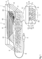
- Figure 1 shows a planar optical element 1 according to an embodiment of the invention.
- the planar optical element 1 has a carrier 2, which is composed of a first layer 21, a second layer 22, and a third layer 23.
- the first layer 21, the second layer 22, and the third layer 23 each contain a polymer as the base material.
- at least one partial area or a partial volume can also be provided with nanoparticles containing, for example, TiO 2. This can influence the optical properties of the first layer 21.
- the second layer 22 and the third layer 23 contain, in addition to the base material, nanowires 3.
- the nanowires 3 are introduced into each layer with a preferred direction, i.e. the longitudinal extensions of the individual nanowires 3 run approximately parallel to one another and approximately parallel to a predetermined desired direction.
- the first side 211 of the first layer 21 forms the surface of the carrier 2.
- the second side 212 of the first layer 21 lies on the first side 221 of the second layer 22.
- the interface can be connected over its entire surface by welding, gluing, or lamination.
- the second side 222 of the second layer 22 lies on the first side 232 of the third layer 23.
- a fully adhesive connection can also be provided at this interface.
- the second side 223 of the third layer 23 forms the underside of the carrier 2.
- the longitudinal extensions of the nanowires 3 in the second layer 22 run approximately orthogonal to the longitudinal extension of the nanotubes 3 of the third layer 23. This results in mechanical stabilization or stabilization against thermal expansion in both spatial directions, so that the photonic component 4 on the carrier 2 is little affected by thermal expansion or force.
- the nanowires 3 can be arranged over the entire surface of the carrier 2, so that the entire carrier 2 is insensitive to thermal expansion, i.e., the change in length or width as a function of temperature is small.
- the first layer 21, the second layer 22, and the third layer 23 can each have a thickness of approximately 25 ⁇ m to approximately 250 ⁇ m or of approximately 50 ⁇ m to approximately 125 ⁇ m. At least one of the layers 21, 22, or 23 can be produced by extrusion, rolling, or wet chemical deposition.
- An arrayed waveguide grating 43 is shown as an example of a photonic component 4.
- the arrayed waveguide grating can be used as an optical microspectrometer, i.e., input signals of different wavelengths are imaged at different locations of the output.
- the optical input signal is fed to the planar optical element 1 via an optical waveguide 50, which can be provided with an optional connector 51.
- the input signal is transmitted via the waveguide 50 into the integrated waveguide 41.
- the waveguide 41 forwards the input signal to the free propagation region 431 of the arrayed waveguide grating 43.
- the free propagation region 431 has an approximately triangular base area.
- a plurality of waveguides 432 are located.
- the waveguides 432 have different lengths and guide the optical input signal from the propagation region 431 to the interference region 433. There, the different wavelengths are caused to interfere.
- an interference pattern is formed, with different wavelengths being imaged at different locations.
- the individual components of the arrayed waveguide grating 43 can be introduced into the first layer 21, for example, by a nanoprinting process.
- the components can be created in the first layer 21 by material modification with a laser or by conventional photolithography.
- a conventional polymer carrier would expand or contract with changes in temperature, causing the geometric dimensions of the arrayed waveguide grating 43 to change. This would impair the performance of the arrayed waveguide grating 43.
- the carrier 2 made of a polymer material offers the advantage over known silicon substrates that even very large carriers can be produced cost-effectively, so that large photonic components or many photonic components can be produced cost-effectively.
- An arrayed waveguide grating with larger dimensions can have improved channel spacings, for example, more than 400 GHz, more than 600 GHz or more than 1 THz.
- additional or other photonic components can be arranged on the carrier 2.
- couplers, fiber Bragg gratings, fiber optic sensors, or waveguides and components derived therefrom can be produced in the first layer 21.
- Figure 2 shows an embodiment of a sensor element which is arranged on a carrier 2.
- the carrier 2 can be composed of at least two layers, as described above with reference to Figure 1 has already been explained.
- the carrier 2 has a partial surface 225 reinforced with nanowires 3.
- nanowires 3 For reasons of clarity, only a few nanowires 3 are shown with their orientation. Of course, however, the nanowires 3 can occupy the entire partial surface 225 and be arranged in several different orientations in one or more layers. It is only essential that the nanowires 3 achieve a sufficiently small expansion for at least one temperature range so that the components arranged in the surface region 225 are not unduly influenced by acting forces and/or temperature fluctuations.
- the remaining surface area of the carrier 2 is provided with fiber optic sensors 45a, 45b, and 45c.
- the invention does not teach the use of exactly three fiber optic sensors 45. Rather, the selected number can be greater or lesser, for example, from 1 to approximately 50.
- Each of the fiber optic sensors 45 has a core 411 whose refractive index is greater than the refractive index of the first layer 21 of the carrier 2. As a result, light is guided in the core 411, resulting in a waveguide 41.
- the waveguides are arranged in a straight line. Of course, meandering or spiral arrangements of at least one waveguide 41 can also be realized.
- At least one fiber Bragg grating 44 is arranged in the core 411 of the waveguide 41.
- each core 41 has seven fiber Bragg gratings 44. In other embodiments of the invention, the number may be greater or lesser. Furthermore, different numbers of fiber Bragg gratings 44 may be arranged in different waveguides 41.
- the optical waveguide 41 and/or the fiber Bragg gratings 44 can be produced in the carrier 2 by laser material processing and/or nanoprinting.
- the carrier 2 does not contain any stabilizing nanowires in the area of the fiber optic sensors 45, the lattice constant of the fiber Bragg gratings 44 changes when force and/or temperature are applied. This changes the spectrum reflected by the respective gratings 40.
- the light reflected by the fiber Bragg gratings 44 is analyzed by the spectrometer arranged in the surface area 225.
- the light is expanded by two couplers 42a and 42b into three optical paths, each of which is connected to a fiber optic sensor 45.
- the light reflected by the fiber Bragg gratings 44 is guided via further couplers 42c, 42d, and 42e to three arrayed waveguide gratings 43a, 43b, and 43c. These provide an optical signal to the output waveguides 435. , which can be converted into electrical signals, for example, via a CCD array or a photodiode array.
- the magnitude of the optical signal is thus a measure of the intensity of the light reflected by the respective fiber Bragg grating 44 and thus a measure of the temperature and/or force prevailing at the location of the respective grating 44. If the same temperature acts on the area 225, the spectrometer remains essentially unaffected, since the nanowires 3 provide mechanical stabilization of this partial area of the carrier 2.
- the invention thus discloses for the first time the integration of a fiber optic sensor and the associated signal readout on a carrier 2.
- Figure 3 shows a possible application of the sensor element from Figure 2 or the planar optical element according to Figure 1 .
- Figure 3 shows a battery housing 6, which can contain a plurality of battery cells to provide a battery with a predeterminable electrical voltage and/or a predeterminable current delivery capacity.
- the battery housing 6 has at least two connection contacts 61 and 62 on its exterior, via which current can be drawn from the battery or a charging current can be supplied.
- a fiber optic sensor 45 can be provided, which contains a plurality of fiber Bragg gratings 44, as described above with reference to Figure 2
- the battery housing 6 can be configured accordingly so that the temperature of the battery cells can be determined at the respective location of the fiber Bragg grating 44.
- the fiber optic sensor 45 is formed on a carrier 2, which is glued to the battery housing 6 or embedded in the material of the battery housing 6. As described above, the carrier 2 has a surface area 225 stabilized by nanowires 3. Located in this area is a planar optical spectrometer in the form of an arrayed waveguide grating 43.
- the light for querying the respective lattice constants of the arrayed waveguide gratings 44 can be coupled in via the waveguide 41 and the coupler 42, as described above.
- the proposed sensor element only requires the connection of a light source and an electronic evaluation circuit to monitor the temperature of a plurality of battery cells.
- the sensor element and the spectrometer required for readout can be embedded on the carrier 2 in the material of the housing 6, thus providing a mechanically robust structure that can withstand even harsh operating conditions without damage, such as those that can occur in vehicles.
- the materials used can be produced inexpensively, making mass market use easy.
Landscapes
- Physics & Mathematics (AREA)
- General Physics & Mathematics (AREA)
- Engineering & Computer Science (AREA)
- Optics & Photonics (AREA)
- Microelectronics & Electronic Packaging (AREA)
- Chemical & Material Sciences (AREA)
- Nanotechnology (AREA)
- Optical Integrated Circuits (AREA)
- Investigating Or Analysing Materials By Optical Means (AREA)
- Light Receiving Elements (AREA)
- Lasers (AREA)
Claims (12)
- Elément optique planaire (1) comprenant au moins un composant photonique (4) disposé dans au moins un support (2),
caractérisé en ce que
le support (2) présente au moins une première couche de film (21) avec une première face (211) et une deuxième face opposée (212) et une deuxième couche de film (22) avec une première face (221) et une deuxième face opposée (222), la première couche de film (21) et la deuxième couche de film contenant ou consistant chacune en au moins un polymère, et la première face (221) de la deuxième couche de film (22) étant disposée sur la deuxième face (212) de la première couche de film (21), la deuxième couche de film (22) contenant, dans au moins une surface partielle (225), des nanofils (3) qui contiennent ou consistent en oxyde de zinc et qui présentent un diamètre d'environ 100 nm à environ 1000 nm, et le composant photonique (4) étant disposé dans la première couche de film (21). - Elément optique planaire selon la revendication 1,
caractérisé en ce que les nanofils (3) ont une longueur d'environ 1 µm à environ 10 µm. - Elément optique planaire selon la revendication 1 ou 2,
caractérisé en ce que la première couche de film (21) contient en outre des nanoparticules. - Elément optique planaire selon la revendication 3,
caractérisé en ce que les nanoparticules contiennent ou consistent en TiO2 et/ou ZnO et/ou SiO2. - Elément optique planaire selon l'une des revendications 1 à 4, caractérisé en ce que le composant photonique (4) dans la première couche de film est choisi parmi au moins un guide d'ondes (41) et/ou au moins un coupleur (42) et/ou au moins un réseau de guides d'ondes (43) et/ou au moins un réseau de Bragg à fibre (44) et/ou au moins un capteur à fibre optique (45).
- Elément optique planaire selon l'une des revendications 1 à 5, contenant en outre une troisième couche de film (23) avec une première face (231) et une deuxième face opposée (232), la troisième couche de film (23) contenant des nanofils (3) au moins dans une surface partielle (225).
- Elément d'optique planaire selon l'une des revendications 1 à 6, caractérisé en ce que les nanofils (3) présentent une orientation prédéfinissable.
- Procédé de fabrication d'un élément optique planaire (1),
comprenant les étapes suivantes consistant à :- fournir une première couche de film (21) avec une première face (211) et une deuxième face opposée (212), la première couche de film (21) contenant un polymère ;- fournir une deuxième couche de film (22) avec une première face (221) et une deuxième face opposée (222), la deuxième couche de film (22) contenant un polymère et, dans au moins une surface partielle (225), des nanofils (3) qui contiennent ou consistent en oxyde de zinc et qui présentent un diamètre d'environ 100 nm à environ 1000 nm,- relier la première face (221) de la deuxième couche de film (22) à la deuxième face (212) de la première couche de film (21),- réaliser au moins un composant photonique (4) dans la première couche de film (21) par modification du matériau par rayonnement laser et/ou nano-impression et/ou photolithographie,- le composant photonique (4) dans la première couche de film (21) étant choisi parmi au moins un guide d'ondes (41) et/ou au moins un coupleur (42) et/ou au moins un réseau de guides d'ondes (43) et/ou au moins un réseau de Bragg à fibres (44) et/ou au moins un capteur à fibre optique (45). - Procédé selon la revendication 8,
comprenant en outre les étapes suivantes consistant à :- fournir une troisième couche de film (23) avec une première face (231) et une deuxième face opposée (232), la troisième couche de film (23) contenant des nanofils (3) dans au moins une surface partielle (225),- stratifier la première face (231) de la troisième couche de film (23) sur la deuxième face (222) de la deuxième couche de film (22). - Procédé selon la revendication 8 ou 9,
dans lequel la première couche de film (21) contient en outre des nanoparticules ou la première couche de film (21) contient en outre des nanoparticules qui contiennent ou consistent en TiO2 et/ou ZnO et/ou SiO2. - Procédé selon l'une des revendications 8 à 10,
dans lequel les nanofils (3) présentent une orientation prédéfinissable. - Procédé selon l'une des revendications 8 à 11,
dans lequel les nanofils (3) ont une longueur d'environ 1 µm à environ 10 µm.
Applications Claiming Priority (2)
| Application Number | Priority Date | Filing Date | Title |
|---|---|---|---|
| DE102012214440A DE102012214440B3 (de) | 2012-08-14 | 2012-08-14 | Planaroptisches Element, Sensorelement und Verfahren zu deren Herstellung |
| PCT/EP2013/066313 WO2014026867A2 (fr) | 2012-08-14 | 2013-08-02 | Élément optique plan, élément de détection et procédé de production correspondant |
Publications (2)
| Publication Number | Publication Date |
|---|---|
| EP2885667A2 EP2885667A2 (fr) | 2015-06-24 |
| EP2885667B1 true EP2885667B1 (fr) | 2025-06-18 |
Family
ID=48998575
Family Applications (1)
| Application Number | Title | Priority Date | Filing Date |
|---|---|---|---|
| EP13750277.9A Active EP2885667B1 (fr) | 2012-08-14 | 2013-08-02 | Élément optique plan, élément de détection et procédé de production correspondant |
Country Status (7)
| Country | Link |
|---|---|
| US (1) | US10120131B2 (fr) |
| EP (1) | EP2885667B1 (fr) |
| JP (1) | JP2015526765A (fr) |
| KR (1) | KR20150054771A (fr) |
| CN (1) | CN104704408B (fr) |
| DE (1) | DE102012214440B3 (fr) |
| WO (1) | WO2014026867A2 (fr) |
Families Citing this family (9)
| Publication number | Priority date | Publication date | Assignee | Title |
|---|---|---|---|---|
| DE112014004084A5 (de) * | 2013-09-05 | 2016-06-09 | Bruker Elemental Gmbh | Optikgrundkörper für Spektrometer, Verfahren zur Herstellung eines Optikgrundkörpers für Spektrometer sowie Spektrometer mit einem solchen Optikgrundkörper |
| DE102014219720B4 (de) * | 2014-09-29 | 2020-07-30 | Fraunhofer-Gesellschaft zur Förderung der angewandten Forschung e.V. | Batterie und Verfahren zu deren Betrieb |
| CN104458064B (zh) * | 2014-11-13 | 2016-06-29 | 中国矿业大学 | 一种矿山压力相似模拟气动支架系统及控制方法 |
| US10408644B2 (en) * | 2016-03-04 | 2019-09-10 | Mitsubishi Electric Corporation | Optical fiber temperature sensor and method for manufacturing same |
| CN109115365A (zh) * | 2018-11-14 | 2019-01-01 | 深圳伊讯科技有限公司 | 一种平面光波导器件及温度测量系统 |
| DE102020113680A1 (de) * | 2020-05-20 | 2021-11-25 | Rosen Swiss Ag | Sensorvorrichtung mit einem eingebetteten optischen Interrogator |
| US11965732B2 (en) * | 2021-02-17 | 2024-04-23 | Touch Netix Limited | Methods and sensor for measuring strain |
| CN113176513A (zh) * | 2021-04-23 | 2021-07-27 | 深圳吉阳智能科技有限公司 | 状态监测单元、状态监测方法及电池 |
| DE102021126080A1 (de) * | 2021-10-07 | 2023-04-13 | Leibniz-Institut für Photonische Technologien e.V. (Engl.Leibniz Institute of Photonic Technology) | Vorrichtung und Verfahren zum Messen einer kryogenen Temperatur sowie Verwendung einer Lichtleitfaser |
Citations (6)
| Publication number | Priority date | Publication date | Assignee | Title |
|---|---|---|---|---|
| JPH11109155A (ja) * | 1997-10-03 | 1999-04-23 | Nippon Telegr & Teleph Corp <Ntt> | 温度無依存導波路 |
| EP1072908A1 (fr) * | 1999-01-13 | 2001-01-31 | The Furukawa Electric Co., Ltd. | Circuit de guide d'ondes optiques et procede pour compenser la longueur d'ondes de la transmission de lumiere |
| JP2003156643A (ja) * | 2001-11-20 | 2003-05-30 | Shinzo Muto | 光学素子及びそれを用いた計測装置 |
| JP2006208982A (ja) * | 2005-01-31 | 2006-08-10 | Kyoto Univ | 低熱膨張性光導波路フィルム |
| JP2009020425A (ja) * | 2007-07-13 | 2009-01-29 | Fujitsu Component Ltd | 光導波路保持部材及び光トランシーバ |
| WO2012098159A2 (fr) * | 2011-01-18 | 2012-07-26 | Fraunhofer-Gesellschaft zur Förderung der angewandten Forschung e.V. | Accumulateur d'énergie électrochimique et procédé permettant d'en déterminer la température |
Family Cites Families (32)
| Publication number | Priority date | Publication date | Assignee | Title |
|---|---|---|---|---|
| CA2007533A1 (fr) * | 1989-01-13 | 1990-07-13 | Bruce Lee Booth | Dispositifs pour guides de lumiere, elements de fabrication de ces dispositifs et methodes de fabrication de ces dispositifs et elements |
| US5716679A (en) | 1991-09-13 | 1998-02-10 | Institut Fur Neue Materialien Gemeinnutzige Gmbh | Optical elements containing nanoscaled particles and having an embossed surface and process for their preparation |
| DE4130550A1 (de) | 1991-09-13 | 1993-03-18 | Inst Neue Mat Gemein Gmbh | Optische elemente und verfahren zu deren herstellung |
| DE4228853C2 (de) * | 1991-09-18 | 1993-10-21 | Schott Glaswerke | Optischer Wellenleiter mit einem planaren oder nur geringfügig gewölbten Substrat und Verfahren zu dessen Herstellung sowie Verwendung eines solchen |
| US7226966B2 (en) * | 2001-08-03 | 2007-06-05 | Nanogram Corporation | Structures incorporating polymer-inorganic particle blends |
| JP2000321442A (ja) * | 1999-05-13 | 2000-11-24 | Sumitomo Electric Ind Ltd | 光部品 |
| CN1330480A (zh) * | 2000-06-27 | 2002-01-09 | 索尼公司 | 字符输入方法及字符输入装置 |
| US6574383B1 (en) * | 2001-04-30 | 2003-06-03 | Massachusetts Institute Of Technology | Input light coupler using a pattern of dielectric contrast distributed in at least two dimensions |
| EP1886802A3 (fr) | 2001-08-03 | 2008-07-30 | NanoGram Corporation | Structure incorporant des mélanges de particules inorganiques-polymères |
| EP1351075A1 (fr) * | 2002-03-19 | 2003-10-08 | Fraunhofer-Gesellschaft zur Förderung der angewandten Forschung e.V. | Méthode de décalage de la longueur d'onde centrale d'un dispositif de guide d'ondes optique par irradiation |
| US7135728B2 (en) * | 2002-09-30 | 2006-11-14 | Nanosys, Inc. | Large-area nanoenabled macroelectronic substrates and uses therefor |
| US6800373B2 (en) * | 2002-10-07 | 2004-10-05 | General Electric Company | Epoxy resin compositions, solid state devices encapsulated therewith and method |
| US7265037B2 (en) * | 2003-06-20 | 2007-09-04 | The Regents Of The University Of California | Nanowire array and nanowire solar cells and methods for forming the same |
| WO2006014582A2 (fr) | 2004-07-08 | 2006-02-09 | Dow Corning Corporation | Interconnexion optique courte portee |
| US7320832B2 (en) * | 2004-12-17 | 2008-01-22 | Integran Technologies Inc. | Fine-grained metallic coatings having the coefficient of thermal expansion matched to the one of the substrate |
| US8703235B2 (en) * | 2007-02-23 | 2014-04-22 | The United States Of America As Represented By The Administrator Of The National Aeronautics And Space Administration | Preparation of metal nanowire decorated carbon allotropes |
| US7865048B2 (en) * | 2006-12-28 | 2011-01-04 | Wisconsin Alumni Research Foundation | Nested waveguides |
| US8134233B2 (en) * | 2007-07-30 | 2012-03-13 | Motorola Solutions, Inc. | Method and apparatus for providing electrically isolated closely spaced features on a printed circuit board |
| JP2009086138A (ja) | 2007-09-28 | 2009-04-23 | Toray Ind Inc | 光学用易接着フィルムおよび光学用積層フィルム |
| CN101553084B (zh) * | 2008-04-01 | 2010-12-08 | 富葵精密组件(深圳)有限公司 | 线路基板及线路基板的制作方法 |
| JP2010018717A (ja) | 2008-07-10 | 2010-01-28 | Hitachi Chem Co Ltd | クラッド形成用樹脂組成物、樹脂フィルム及びそれらを用いた光導波路 |
| WO2010062644A2 (fr) * | 2008-10-28 | 2010-06-03 | The Regents Of The University Of California | Nanofils verticaux des groupes iii à v sur du si, hétérostructures, matrices flexibles et fabrication |
| JP2010129964A (ja) | 2008-12-01 | 2010-06-10 | Kurabo Ind Ltd | フレキシブルプリント配線板補強用シート及びそれを用いたフレキシブルプリント配線板 |
| DE102008064168A1 (de) * | 2008-12-22 | 2010-06-24 | Leibniz-Institut Für Neue Materialien Gemeinnützige Gmbh | Verfahren und Zusammensetzung zur Herstellung optischer Elemente mit Gradientenstruktur |
| JP5182227B2 (ja) * | 2009-06-02 | 2013-04-17 | 住友ベークライト株式会社 | 光信号伝送用基板および電子機器 |
| JP2011034057A (ja) * | 2009-07-10 | 2011-02-17 | Nippon Telegr & Teleph Corp <Ntt> | 光変調器 |
| DE102010001197B4 (de) | 2010-01-25 | 2019-05-29 | Draka Cable Wuppertal Gmbh | Sensorelement und Verfahren zu seiner Herstellung und Verwendung |
| DE102010061831A1 (de) * | 2010-11-24 | 2012-05-24 | Fraunhofer-Gesellschaft zur Förderung der angewandten Forschung e.V. | Halbleiterbauelement und Verfahren zu seiner Herstellung |
| EP2515099A1 (fr) * | 2011-04-21 | 2012-10-24 | Fraunhofer Gesellschaft zur Förderung der angewandten Wissenschaft E.V. | Procédé de détection de molécules et capteur optique |
| DE102011017622B3 (de) | 2011-04-27 | 2012-10-31 | Fraunhofer-Gesellschaft zur Förderung der angewandten Forschung e.V. | Vorrichtung zur Messung von Zustandsgrößen mit einem faseroptischen Sensor und deren Verwendung |
| DE102012222460A1 (de) * | 2012-12-06 | 2014-06-12 | Fraunhofer-Gesellschaft zur Förderung der angewandten Forschung e.V. | Verfahren und Vorrichtung zur Herstellung von zumindest einem Faser-Bragg-Gitter |
| JP2016042159A (ja) * | 2014-08-18 | 2016-03-31 | 富士フイルム株式会社 | 光学フィルム及びその製造方法、偏光板保護フィルム、偏光板並びに液晶表示装置 |
-
2012
- 2012-08-14 DE DE102012214440A patent/DE102012214440B3/de active Active
-
2013
- 2013-08-02 CN CN201380052754.5A patent/CN104704408B/zh active Active
- 2013-08-02 US US14/420,083 patent/US10120131B2/en active Active
- 2013-08-02 KR KR1020157003978A patent/KR20150054771A/ko not_active Ceased
- 2013-08-02 WO PCT/EP2013/066313 patent/WO2014026867A2/fr not_active Ceased
- 2013-08-02 JP JP2015526929A patent/JP2015526765A/ja active Pending
- 2013-08-02 EP EP13750277.9A patent/EP2885667B1/fr active Active
Patent Citations (6)
| Publication number | Priority date | Publication date | Assignee | Title |
|---|---|---|---|---|
| JPH11109155A (ja) * | 1997-10-03 | 1999-04-23 | Nippon Telegr & Teleph Corp <Ntt> | 温度無依存導波路 |
| EP1072908A1 (fr) * | 1999-01-13 | 2001-01-31 | The Furukawa Electric Co., Ltd. | Circuit de guide d'ondes optiques et procede pour compenser la longueur d'ondes de la transmission de lumiere |
| JP2003156643A (ja) * | 2001-11-20 | 2003-05-30 | Shinzo Muto | 光学素子及びそれを用いた計測装置 |
| JP2006208982A (ja) * | 2005-01-31 | 2006-08-10 | Kyoto Univ | 低熱膨張性光導波路フィルム |
| JP2009020425A (ja) * | 2007-07-13 | 2009-01-29 | Fujitsu Component Ltd | 光導波路保持部材及び光トランシーバ |
| WO2012098159A2 (fr) * | 2011-01-18 | 2012-07-26 | Fraunhofer-Gesellschaft zur Förderung der angewandten Forschung e.V. | Accumulateur d'énergie électrochimique et procédé permettant d'en déterminer la température |
Non-Patent Citations (2)
| Title |
|---|
| ION SANDU ET AL: "Synthesis of optical transparent and electrical conductive polymer/nanocarbon composite by infiltration method", THIN SOLID FILMS, ELSEVIER, AMSTERDAM, NL, vol. 519, no. 12, 1 April 2011 (2011-04-01), pages 4128 - 4131, XP002715935, ISSN: 0040-6090, [retrieved on 20110202], DOI: 10.1016/J.TSF.2011.01.361 * |
| NANTAO HU ET AL: "Efficient dispersion of multi-walled carbon nanotubes by in situ polymerization", POLYMER INTERNATIONAL, BARKING, GB, vol. 56, no. 5, 1 May 2007 (2007-05-01), pages 655 - 659, XP002715934, ISSN: 0959-8103, [retrieved on 20061229], DOI: 10.1002/PI.2187 * |
Also Published As
| Publication number | Publication date |
|---|---|
| US10120131B2 (en) | 2018-11-06 |
| JP2015526765A (ja) | 2015-09-10 |
| DE102012214440B3 (de) | 2013-10-24 |
| CN104704408B (zh) | 2018-02-06 |
| CN104704408A (zh) | 2015-06-10 |
| KR20150054771A (ko) | 2015-05-20 |
| EP2885667A2 (fr) | 2015-06-24 |
| US20150219848A1 (en) | 2015-08-06 |
| WO2014026867A3 (fr) | 2014-04-03 |
| WO2014026867A2 (fr) | 2014-02-20 |
Similar Documents
| Publication | Publication Date | Title |
|---|---|---|
| EP2885667B1 (fr) | Élément optique plan, élément de détection et procédé de production correspondant | |
| DE60222696T2 (de) | Chirale faser-laser-vorrichtung und verfahren | |
| EP0840900B1 (fr) | Structure optique et son procede de fabrication | |
| EP0647328B1 (fr) | Element polymere optique pour coupler des cellules photo-electriques a des circuits optiques integres | |
| EP0560412A2 (fr) | Dispositif de spectromètre optique intégré et son procédé de fabrication | |
| EP1533876B1 (fr) | Contrôle de polarisation dans une diode laser verticale utilisant un réseau monolithiquement intégré | |
| EP3373023B1 (fr) | Capteur et son procédé de fabrication et d'utilisation | |
| DE112008000320T5 (de) | Metamaterialstrukturen für Lichtverarbeitung und Verfahren zum Verarbeiten von Licht | |
| EP2702364A1 (fr) | Dispositif pour mesurer des paramètres d'état | |
| DE112018007107B4 (de) | Optische integrierte Halbleitervorrichtung | |
| EP3183607B1 (fr) | Diode optique | |
| DE112016003950T5 (de) | Oberflächenemittierender laser mit zweidimensionalem photonischen kristall | |
| DE112007000664T5 (de) | Zweidimensionaler photonischer Kristall | |
| EP3545347B1 (fr) | Composant optoélectronique et procédé de fabrication d'un composant optoélectronique | |
| DE102012214441A1 (de) | Faseroptischer Sensor und Messverfahren | |
| EP0740802B1 (fr) | Procede de fabrication d'une composante optique integre | |
| EP0831343A2 (fr) | Guide d'ondes optique et son procédé de fabrication | |
| DE112022001742T5 (de) | Monolithisch integrierte optische Baugruppe | |
| EP2274571B1 (fr) | Dispositif de mesure comportant un réseau de bragg de fibre pour la détection de dilatations ou de températures | |
| EP3374808A1 (fr) | Composant optique et procédé de fabrication | |
| WO2005012885A1 (fr) | Capteur d'extension optique sans contact pour la mesure de variations dans la resonance plasmon de particules | |
| DE102020212112A1 (de) | Optisches Wellenleiterbauelement und Verfahren zu dessen Herstellung | |
| DE60115966T2 (de) | Optische filter, ihre herstellungsverfahren und ihre anwendung für ein multiplexsystem | |
| DE112008002444T5 (de) | Elektrische Kontaktvorrichtung für optische Wellenleiter | |
| DE102023209311A1 (de) | Messvorrichtung und Verfahren zu deren Herstellung und Verwendung |
Legal Events
| Date | Code | Title | Description |
|---|---|---|---|
| PUAI | Public reference made under article 153(3) epc to a published international application that has entered the european phase |
Free format text: ORIGINAL CODE: 0009012 |
|
| 17P | Request for examination filed |
Effective date: 20150120 |
|
| AK | Designated contracting states |
Kind code of ref document: A2 Designated state(s): AL AT BE BG CH CY CZ DE DK EE ES FI FR GB GR HR HU IE IS IT LI LT LU LV MC MK MT NL NO PL PT RO RS SE SI SK SM TR |
|
| AX | Request for extension of the european patent |
Extension state: BA ME |
|
| DAX | Request for extension of the european patent (deleted) | ||
| STAA | Information on the status of an ep patent application or granted ep patent |
Free format text: STATUS: EXAMINATION IS IN PROGRESS |
|
| PUAG | Search results despatched under rule 164(2) epc together with communication from examining division |
Free format text: ORIGINAL CODE: 0009017 |
|
| 17Q | First examination report despatched |
Effective date: 20191104 |
|
| B565 | Issuance of search results under rule 164(2) epc |
Effective date: 20191104 |
|
| RIC1 | Information provided on ipc code assigned before grant |
Ipc: G02B 6/138 20060101AFI20191029BHEP |
|
| RAP3 | Party data changed (applicant data changed or rights of an application transferred) |
Owner name: FRAUNHOFER-GESELLSCHAFT ZUR FOERDERUNG DER ANGEWANDTEN FORSCHUNG E.V. |
|
| REG | Reference to a national code |
Ref country code: DE Ref legal event code: R079 Free format text: PREVIOUS MAIN CLASS: G02B0006138000 Ipc: G01K0011320600 Ref country code: DE Ref legal event code: R079 Ref document number: 502013016592 Country of ref document: DE Free format text: PREVIOUS MAIN CLASS: G02B0006138000 Ipc: G01K0011320600 |
|
| GRAP | Despatch of communication of intention to grant a patent |
Free format text: ORIGINAL CODE: EPIDOSNIGR1 |
|
| STAA | Information on the status of an ep patent application or granted ep patent |
Free format text: STATUS: GRANT OF PATENT IS INTENDED |
|
| RIC1 | Information provided on ipc code assigned before grant |
Ipc: G02B 6/293 20060101ALN20250207BHEP Ipc: G02B 6/12 20060101ALN20250207BHEP Ipc: G02B 6/122 20060101ALI20250207BHEP Ipc: G02B 6/132 20060101ALI20250207BHEP Ipc: G01L 1/24 20060101ALI20250207BHEP Ipc: G01K 11/3206 20210101AFI20250207BHEP |
|
| INTG | Intention to grant announced |
Effective date: 20250227 |
|
| GRAS | Grant fee paid |
Free format text: ORIGINAL CODE: EPIDOSNIGR3 |
|
| GRAA | (expected) grant |
Free format text: ORIGINAL CODE: 0009210 |
|
| STAA | Information on the status of an ep patent application or granted ep patent |
Free format text: STATUS: THE PATENT HAS BEEN GRANTED |
|
| AK | Designated contracting states |
Kind code of ref document: B1 Designated state(s): AL AT BE BG CH CY CZ DE DK EE ES FI FR GB GR HR HU IE IS IT LI LT LU LV MC MK MT NL NO PL PT RO RS SE SI SK SM TR |
|
| REG | Reference to a national code |
Ref country code: GB Ref legal event code: FG4D Free format text: NOT ENGLISH |
|
| REG | Reference to a national code |
Ref country code: CH Ref legal event code: EP |
|
| REG | Reference to a national code |
Ref country code: DE Ref legal event code: R096 Ref document number: 502013016592 Country of ref document: DE |
|
| REG | Reference to a national code |
Ref country code: CH Ref legal event code: EP |
|
| REG | Reference to a national code |
Ref country code: IE Ref legal event code: FG4D Free format text: LANGUAGE OF EP DOCUMENT: GERMAN |
|
| PG25 | Lapsed in a contracting state [announced via postgrant information from national office to epo] |
Ref country code: FI Free format text: LAPSE BECAUSE OF FAILURE TO SUBMIT A TRANSLATION OF THE DESCRIPTION OR TO PAY THE FEE WITHIN THE PRESCRIBED TIME-LIMIT Effective date: 20250618 |
|
| PGFP | Annual fee paid to national office [announced via postgrant information from national office to epo] |
Ref country code: DE Payment date: 20250819 Year of fee payment: 13 |
|
| REG | Reference to a national code |
Ref country code: LT Ref legal event code: MG9D |
|
| PG25 | Lapsed in a contracting state [announced via postgrant information from national office to epo] |
Ref country code: GR Free format text: LAPSE BECAUSE OF FAILURE TO SUBMIT A TRANSLATION OF THE DESCRIPTION OR TO PAY THE FEE WITHIN THE PRESCRIBED TIME-LIMIT Effective date: 20250919 Ref country code: NO Free format text: LAPSE BECAUSE OF FAILURE TO SUBMIT A TRANSLATION OF THE DESCRIPTION OR TO PAY THE FEE WITHIN THE PRESCRIBED TIME-LIMIT Effective date: 20250918 |
|
| PG25 | Lapsed in a contracting state [announced via postgrant information from national office to epo] |
Ref country code: BG Free format text: LAPSE BECAUSE OF FAILURE TO SUBMIT A TRANSLATION OF THE DESCRIPTION OR TO PAY THE FEE WITHIN THE PRESCRIBED TIME-LIMIT Effective date: 20250618 |
|
| PGFP | Annual fee paid to national office [announced via postgrant information from national office to epo] |
Ref country code: GB Payment date: 20250822 Year of fee payment: 13 |
|
| PG25 | Lapsed in a contracting state [announced via postgrant information from national office to epo] |
Ref country code: HR Free format text: LAPSE BECAUSE OF FAILURE TO SUBMIT A TRANSLATION OF THE DESCRIPTION OR TO PAY THE FEE WITHIN THE PRESCRIBED TIME-LIMIT Effective date: 20250618 |
|
| PGFP | Annual fee paid to national office [announced via postgrant information from national office to epo] |
Ref country code: FR Payment date: 20250821 Year of fee payment: 13 |
|
| PG25 | Lapsed in a contracting state [announced via postgrant information from national office to epo] |
Ref country code: RS Free format text: LAPSE BECAUSE OF FAILURE TO SUBMIT A TRANSLATION OF THE DESCRIPTION OR TO PAY THE FEE WITHIN THE PRESCRIBED TIME-LIMIT Effective date: 20250918 |
|
| REG | Reference to a national code |
Ref country code: NL Ref legal event code: MP Effective date: 20250618 |
|
| PG25 | Lapsed in a contracting state [announced via postgrant information from national office to epo] |
Ref country code: LV Free format text: LAPSE BECAUSE OF FAILURE TO SUBMIT A TRANSLATION OF THE DESCRIPTION OR TO PAY THE FEE WITHIN THE PRESCRIBED TIME-LIMIT Effective date: 20250618 |
|
| PG25 | Lapsed in a contracting state [announced via postgrant information from national office to epo] |
Ref country code: NL Free format text: LAPSE BECAUSE OF FAILURE TO SUBMIT A TRANSLATION OF THE DESCRIPTION OR TO PAY THE FEE WITHIN THE PRESCRIBED TIME-LIMIT Effective date: 20250618 |
|
| PG25 | Lapsed in a contracting state [announced via postgrant information from national office to epo] |
Ref country code: PT Free format text: LAPSE BECAUSE OF FAILURE TO SUBMIT A TRANSLATION OF THE DESCRIPTION OR TO PAY THE FEE WITHIN THE PRESCRIBED TIME-LIMIT Effective date: 20251020 |
|
| PG25 | Lapsed in a contracting state [announced via postgrant information from national office to epo] |
Ref country code: IS Free format text: LAPSE BECAUSE OF FAILURE TO SUBMIT A TRANSLATION OF THE DESCRIPTION OR TO PAY THE FEE WITHIN THE PRESCRIBED TIME-LIMIT Effective date: 20251018 |
|
| PG25 | Lapsed in a contracting state [announced via postgrant information from national office to epo] |
Ref country code: SM Free format text: LAPSE BECAUSE OF FAILURE TO SUBMIT A TRANSLATION OF THE DESCRIPTION OR TO PAY THE FEE WITHIN THE PRESCRIBED TIME-LIMIT Effective date: 20250618 |
|
| PG25 | Lapsed in a contracting state [announced via postgrant information from national office to epo] |
Ref country code: CZ Free format text: LAPSE BECAUSE OF FAILURE TO SUBMIT A TRANSLATION OF THE DESCRIPTION OR TO PAY THE FEE WITHIN THE PRESCRIBED TIME-LIMIT Effective date: 20250618 |
|
| PG25 | Lapsed in a contracting state [announced via postgrant information from national office to epo] |
Ref country code: PL Free format text: LAPSE BECAUSE OF FAILURE TO SUBMIT A TRANSLATION OF THE DESCRIPTION OR TO PAY THE FEE WITHIN THE PRESCRIBED TIME-LIMIT Effective date: 20250618 |
|
| PG25 | Lapsed in a contracting state [announced via postgrant information from national office to epo] |
Ref country code: EE Free format text: LAPSE BECAUSE OF FAILURE TO SUBMIT A TRANSLATION OF THE DESCRIPTION OR TO PAY THE FEE WITHIN THE PRESCRIBED TIME-LIMIT Effective date: 20250618 |
|
| PG25 | Lapsed in a contracting state [announced via postgrant information from national office to epo] |
Ref country code: SK Free format text: LAPSE BECAUSE OF FAILURE TO SUBMIT A TRANSLATION OF THE DESCRIPTION OR TO PAY THE FEE WITHIN THE PRESCRIBED TIME-LIMIT Effective date: 20250618 Ref country code: RO Free format text: LAPSE BECAUSE OF FAILURE TO SUBMIT A TRANSLATION OF THE DESCRIPTION OR TO PAY THE FEE WITHIN THE PRESCRIBED TIME-LIMIT Effective date: 20250618 |
|
| PG25 | Lapsed in a contracting state [announced via postgrant information from national office to epo] |
Ref country code: ES Free format text: LAPSE BECAUSE OF FAILURE TO SUBMIT A TRANSLATION OF THE DESCRIPTION OR TO PAY THE FEE WITHIN THE PRESCRIBED TIME-LIMIT Effective date: 20250618 |
|
| REG | Reference to a national code |
Ref country code: CH Ref legal event code: H13 Free format text: ST27 STATUS EVENT CODE: U-0-0-H10-H13 (AS PROVIDED BY THE NATIONAL OFFICE) Effective date: 20260324 |
|
| PG25 | Lapsed in a contracting state [announced via postgrant information from national office to epo] |
Ref country code: MC Free format text: LAPSE BECAUSE OF FAILURE TO SUBMIT A TRANSLATION OF THE DESCRIPTION OR TO PAY THE FEE WITHIN THE PRESCRIBED TIME-LIMIT Effective date: 20250618 |
|
| PG25 | Lapsed in a contracting state [announced via postgrant information from national office to epo] |
Ref country code: DK Free format text: LAPSE BECAUSE OF FAILURE TO SUBMIT A TRANSLATION OF THE DESCRIPTION OR TO PAY THE FEE WITHIN THE PRESCRIBED TIME-LIMIT Effective date: 20250618 |
|
| PG25 | Lapsed in a contracting state [announced via postgrant information from national office to epo] |
Ref country code: LU Free format text: LAPSE BECAUSE OF NON-PAYMENT OF DUE FEES Effective date: 20250802 Ref country code: IT Free format text: LAPSE BECAUSE OF FAILURE TO SUBMIT A TRANSLATION OF THE DESCRIPTION OR TO PAY THE FEE WITHIN THE PRESCRIBED TIME-LIMIT Effective date: 20250618 |
|
| PG25 | Lapsed in a contracting state [announced via postgrant information from national office to epo] |
Ref country code: CH Free format text: LAPSE BECAUSE OF NON-PAYMENT OF DUE FEES Effective date: 20250831 |
|
| PLBE | No opposition filed within time limit |
Free format text: ORIGINAL CODE: 0009261 |
|
| STAA | Information on the status of an ep patent application or granted ep patent |
Free format text: STATUS: NO OPPOSITION FILED WITHIN TIME LIMIT |
|
| REG | Reference to a national code |
Ref country code: CH Ref legal event code: L10 Free format text: ST27 STATUS EVENT CODE: U-0-0-L10-L00 (AS PROVIDED BY THE NATIONAL OFFICE) Effective date: 20260430 |