EP2894697A1 - Strukturformungsverfahren, strukturen, verfahren zur herstellung ineinandergreifender elektroden und wiederaufladbare batterie - Google Patents
Strukturformungsverfahren, strukturen, verfahren zur herstellung ineinandergreifender elektroden und wiederaufladbare batterie Download PDFInfo
- Publication number
- EP2894697A1 EP2894697A1 EP13835967.4A EP13835967A EP2894697A1 EP 2894697 A1 EP2894697 A1 EP 2894697A1 EP 13835967 A EP13835967 A EP 13835967A EP 2894697 A1 EP2894697 A1 EP 2894697A1
- Authority
- EP
- European Patent Office
- Prior art keywords
- comb
- pattern
- forming
- guide hole
- resist layer
- Prior art date
- Legal status (The legal status is an assumption and is not a legal conclusion. Google has not performed a legal analysis and makes no representation as to the accuracy of the status listed.)
- Granted
Links
Images




Classifications
-
- H—ELECTRICITY
- H01—ELECTRIC ELEMENTS
- H01M—PROCESSES OR MEANS, e.g. BATTERIES, FOR THE DIRECT CONVERSION OF CHEMICAL ENERGY INTO ELECTRICAL ENERGY
- H01M4/00—Electrodes
- H01M4/02—Electrodes composed of, or comprising, active material
- H01M4/04—Processes of manufacture in general
- H01M4/0402—Methods of deposition of the material
- H01M4/0414—Methods of deposition of the material by screen printing
-
- G—PHYSICS
- G03—PHOTOGRAPHY; CINEMATOGRAPHY; ANALOGOUS TECHNIQUES USING WAVES OTHER THAN OPTICAL WAVES; ELECTROGRAPHY; HOLOGRAPHY
- G03F—PHOTOMECHANICAL PRODUCTION OF TEXTURED OR PATTERNED SURFACES, e.g. FOR PRINTING, FOR PROCESSING OF SEMICONDUCTOR DEVICES; MATERIALS THEREFOR; ORIGINALS THEREFOR; APPARATUS SPECIALLY ADAPTED THEREFOR
- G03F7/00—Photomechanical, e.g. photolithographic, production of textured or patterned surfaces, e.g. printing surfaces; Materials therefor, e.g. comprising photoresists; Apparatus specially adapted therefor
- G03F7/0035—Multiple processes, e.g. applying a further resist layer on an already in a previously step, processed pattern or textured surface
-
- H—ELECTRICITY
- H01—ELECTRIC ELEMENTS
- H01M—PROCESSES OR MEANS, e.g. BATTERIES, FOR THE DIRECT CONVERSION OF CHEMICAL ENERGY INTO ELECTRICAL ENERGY
- H01M10/00—Secondary cells; Manufacture thereof
- H01M10/05—Accumulators with non-aqueous electrolyte
- H01M10/058—Construction or manufacture
-
- H—ELECTRICITY
- H01—ELECTRIC ELEMENTS
- H01M—PROCESSES OR MEANS, e.g. BATTERIES, FOR THE DIRECT CONVERSION OF CHEMICAL ENERGY INTO ELECTRICAL ENERGY
- H01M4/00—Electrodes
- H01M4/02—Electrodes composed of, or comprising, active material
- H01M4/04—Processes of manufacture in general
- H01M4/0402—Methods of deposition of the material
- H01M4/0404—Methods of deposition of the material by coating on electrode collectors
-
- H—ELECTRICITY
- H01—ELECTRIC ELEMENTS
- H01M—PROCESSES OR MEANS, e.g. BATTERIES, FOR THE DIRECT CONVERSION OF CHEMICAL ENERGY INTO ELECTRICAL ENERGY
- H01M4/00—Electrodes
- H01M4/02—Electrodes composed of, or comprising, active material
- H01M4/13—Electrodes for accumulators with non-aqueous electrolyte, e.g. for lithium-accumulators; Processes of manufacture thereof
-
- H—ELECTRICITY
- H01—ELECTRIC ELEMENTS
- H01M—PROCESSES OR MEANS, e.g. BATTERIES, FOR THE DIRECT CONVERSION OF CHEMICAL ENERGY INTO ELECTRICAL ENERGY
- H01M4/00—Electrodes
- H01M4/02—Electrodes composed of, or comprising, active material
- H01M4/13—Electrodes for accumulators with non-aqueous electrolyte, e.g. for lithium-accumulators; Processes of manufacture thereof
- H01M4/139—Processes of manufacture
-
- H—ELECTRICITY
- H01—ELECTRIC ELEMENTS
- H01M—PROCESSES OR MEANS, e.g. BATTERIES, FOR THE DIRECT CONVERSION OF CHEMICAL ENERGY INTO ELECTRICAL ENERGY
- H01M4/00—Electrodes
- H01M4/02—Electrodes composed of, or comprising, active material
- H01M4/64—Carriers or collectors
- H01M4/70—Carriers or collectors characterised by shape or form
-
- H—ELECTRICITY
- H01—ELECTRIC ELEMENTS
- H01M—PROCESSES OR MEANS, e.g. BATTERIES, FOR THE DIRECT CONVERSION OF CHEMICAL ENERGY INTO ELECTRICAL ENERGY
- H01M6/00—Primary cells; Manufacture thereof
- H01M6/40—Printed batteries, e.g. thin film batteries
-
- G—PHYSICS
- G03—PHOTOGRAPHY; CINEMATOGRAPHY; ANALOGOUS TECHNIQUES USING WAVES OTHER THAN OPTICAL WAVES; ELECTROGRAPHY; HOLOGRAPHY
- G03F—PHOTOMECHANICAL PRODUCTION OF TEXTURED OR PATTERNED SURFACES, e.g. FOR PRINTING, FOR PROCESSING OF SEMICONDUCTOR DEVICES; MATERIALS THEREFOR; ORIGINALS THEREFOR; APPARATUS SPECIALLY ADAPTED THEREFOR
- G03F7/00—Photomechanical, e.g. photolithographic, production of textured or patterned surfaces, e.g. printing surfaces; Materials therefor, e.g. comprising photoresists; Apparatus specially adapted therefor
- G03F7/0037—Production of three-dimensional images
-
- G—PHYSICS
- G03—PHOTOGRAPHY; CINEMATOGRAPHY; ANALOGOUS TECHNIQUES USING WAVES OTHER THAN OPTICAL WAVES; ELECTROGRAPHY; HOLOGRAPHY
- G03F—PHOTOMECHANICAL PRODUCTION OF TEXTURED OR PATTERNED SURFACES, e.g. FOR PRINTING, FOR PROCESSING OF SEMICONDUCTOR DEVICES; MATERIALS THEREFOR; ORIGINALS THEREFOR; APPARATUS SPECIALLY ADAPTED THEREFOR
- G03F7/00—Photomechanical, e.g. photolithographic, production of textured or patterned surfaces, e.g. printing surfaces; Materials therefor, e.g. comprising photoresists; Apparatus specially adapted therefor
- G03F7/12—Production of screen printing forms or similar printing forms, e.g. stencils
-
- G—PHYSICS
- G03—PHOTOGRAPHY; CINEMATOGRAPHY; ANALOGOUS TECHNIQUES USING WAVES OTHER THAN OPTICAL WAVES; ELECTROGRAPHY; HOLOGRAPHY
- G03F—PHOTOMECHANICAL PRODUCTION OF TEXTURED OR PATTERNED SURFACES, e.g. FOR PRINTING, FOR PROCESSING OF SEMICONDUCTOR DEVICES; MATERIALS THEREFOR; ORIGINALS THEREFOR; APPARATUS SPECIALLY ADAPTED THEREFOR
- G03F7/00—Photomechanical, e.g. photolithographic, production of textured or patterned surfaces, e.g. printing surfaces; Materials therefor, e.g. comprising photoresists; Apparatus specially adapted therefor
- G03F7/26—Processing photosensitive materials; Apparatus therefor
- G03F7/40—Treatment after imagewise removal, e.g. baking
-
- H—ELECTRICITY
- H01—ELECTRIC ELEMENTS
- H01M—PROCESSES OR MEANS, e.g. BATTERIES, FOR THE DIRECT CONVERSION OF CHEMICAL ENERGY INTO ELECTRICAL ENERGY
- H01M10/00—Secondary cells; Manufacture thereof
- H01M10/05—Accumulators with non-aqueous electrolyte
- H01M10/052—Li-accumulators
-
- H—ELECTRICITY
- H01—ELECTRIC ELEMENTS
- H01M—PROCESSES OR MEANS, e.g. BATTERIES, FOR THE DIRECT CONVERSION OF CHEMICAL ENERGY INTO ELECTRICAL ENERGY
- H01M10/00—Secondary cells; Manufacture thereof
- H01M10/05—Accumulators with non-aqueous electrolyte
- H01M10/056—Accumulators with non-aqueous electrolyte characterised by the materials used as electrolytes, e.g. mixed inorganic/organic electrolytes
- H01M10/0564—Accumulators with non-aqueous electrolyte characterised by the materials used as electrolytes, e.g. mixed inorganic/organic electrolytes the electrolyte being constituted of organic materials only
- H01M10/0565—Polymeric materials, e.g. gel-type or solid-type
-
- H—ELECTRICITY
- H01—ELECTRIC ELEMENTS
- H01M—PROCESSES OR MEANS, e.g. BATTERIES, FOR THE DIRECT CONVERSION OF CHEMICAL ENERGY INTO ELECTRICAL ENERGY
- H01M4/00—Electrodes
- H01M4/02—Electrodes composed of, or comprising, active material
- H01M2004/025—Electrodes composed of, or comprising, active material with shapes other than plane or cylindrical
-
- H—ELECTRICITY
- H10—SEMICONDUCTOR DEVICES; ELECTRIC SOLID-STATE DEVICES NOT OTHERWISE PROVIDED FOR
- H10P—GENERIC PROCESSES OR APPARATUS FOR THE MANUFACTURE OR TREATMENT OF DEVICES COVERED BY CLASS H10
- H10P14/00—Formation of materials, e.g. in the shape of layers or pillars
- H10P14/40—Formation of materials, e.g. in the shape of layers or pillars of conductive or resistive materials
- H10P14/46—Formation of materials, e.g. in the shape of layers or pillars of conductive or resistive materials using a liquid
-
- H—ELECTRICITY
- H10—SEMICONDUCTOR DEVICES; ELECTRIC SOLID-STATE DEVICES NOT OTHERWISE PROVIDED FOR
- H10W—GENERIC PACKAGES, INTERCONNECTIONS, CONNECTORS OR OTHER CONSTRUCTIONAL DETAILS OF DEVICES COVERED BY CLASS H10
- H10W20/00—Interconnections in chips, wafers or substrates
- H10W20/01—Manufacture or treatment
- H10W20/031—Manufacture or treatment of conductive parts of the interconnections
- H10W20/063—Manufacture or treatment of conductive parts of the interconnections by forming conductive members before forming protective insulating material
-
- Y—GENERAL TAGGING OF NEW TECHNOLOGICAL DEVELOPMENTS; GENERAL TAGGING OF CROSS-SECTIONAL TECHNOLOGIES SPANNING OVER SEVERAL SECTIONS OF THE IPC; TECHNICAL SUBJECTS COVERED BY FORMER USPC CROSS-REFERENCE ART COLLECTIONS [XRACs] AND DIGESTS
- Y02—TECHNOLOGIES OR APPLICATIONS FOR MITIGATION OR ADAPTATION AGAINST CLIMATE CHANGE
- Y02E—REDUCTION OF GREENHOUSE GAS [GHG] EMISSIONS, RELATED TO ENERGY GENERATION, TRANSMISSION OR DISTRIBUTION
- Y02E60/00—Enabling technologies; Technologies with a potential or indirect contribution to GHG emissions mitigation
- Y02E60/10—Energy storage using batteries
-
- Y—GENERAL TAGGING OF NEW TECHNOLOGICAL DEVELOPMENTS; GENERAL TAGGING OF CROSS-SECTIONAL TECHNOLOGIES SPANNING OVER SEVERAL SECTIONS OF THE IPC; TECHNICAL SUBJECTS COVERED BY FORMER USPC CROSS-REFERENCE ART COLLECTIONS [XRACs] AND DIGESTS
- Y02—TECHNOLOGIES OR APPLICATIONS FOR MITIGATION OR ADAPTATION AGAINST CLIMATE CHANGE
- Y02P—CLIMATE CHANGE MITIGATION TECHNOLOGIES IN THE PRODUCTION OR PROCESSING OF GOODS
- Y02P70/00—Climate change mitigation technologies in the production process for final industrial or consumer products
- Y02P70/50—Manufacturing or production processes characterised by the final manufactured product
Definitions
- the present invention relates to a method for forming a pattern in which a plurality of patterns of identical or different pattern materials are formed on a support, a structural body comprising the pattern formed by the method for forming a pattern, a method for producing a comb-shaped electrode using the method for forming a pattern, and a secondary cell comprising the comb-shaped electrode produced by the production method.
- the present invention has been made in view of the problems described above; and it is an object of the present invention to provide a method for forming a pattern in which a plurality of patterns of identical or different pattern materials can be formed on a support in a short time, a structural body comprising the pattern formed by the method for forming a pattern, a method for forming a comb-shaped electrode using the method for forming a pattern, and a secondary cell comprising the comb-shaped electrode produced by the production method.
- the present inventors have thoroughly investigated to solve the problems described above. As a result, it has been found that the above-mentioned problems can be solved by way of filling a pattern material into a guide hole by a screen printing process when forming a pattern, thereby completing the present invention. Specifically, the present invention provides the following.
- a second aspect of the present invention relates to a structural body comprising the pattern formed by the method for forming a pattern.
- a third aspect of the present invention relates to a method for producing a comb-shaped electrode, in which a positive electrode and a negative electrode are each formed into a comb shape and oppositely disposed so that parts of teeth of the comb shapes are alternately arranged; and the method includes forming a conductive layer on a surface of a substrate, forming a current collector by patterning the conductive layer, and forming the positive electrode and the negative electrode on the current collector using the method for forming a pattern.
- a fourth aspect of the present invention relates to a secondary cell comprising the comb-shaped electrode produced by the above-mentioned production method.
- a method for forming a pattern in which a plurality of patterns of identical or different pattern materials can be formed on a support in a short time a structural body comprising the pattern formed by the method for forming a pattern, a method for producing a comb-shaped electrode using the method for forming a pattern, and a secondary cell comprising the comb-shaped electrode produced by the production method.
- FIGs. 1A to 1H are transverse sectional views showing the method for forming a pattern in accordance with an embodiment of the present invention.
- the pattern forming method in accordance with the embodiment of the present invention is explained with reference to FIGs. 1A to 1H .
- the first resist layer 2 is formed by coating a positive-type resist composition on the surface of the support 1 shown in FIG. 1A .
- the guide holes 3a and 3b are formed in order to form the pattern material layers 4a and 4b, as described later.
- the guide holes 3a and 3b become a casting mold when forming the pattern material layers 4a and 4b and thus are required to have sufficient depth for forming the pattern material layers 4a and 4b.
- the thickness of the first resist layer 2 becomes the future depth of the guide holes 3a and 3b and thus is appropriately set considering the necessary depth of the guide holes 3a and 3b.
- the thickness of the first resist layer 2 may be exemplified by 10 to 100 ⁇ m, without particular limitation thereto.
- the positive-type resist composition used for forming the first resist layer 2 may be conventional ones without particular limitation thereto and may be non-chemical amplification type or chemical amplification type.
- the non-chemical amplification-type positive-type resist composition may be exemplified by those containing at least a quinonediazide group-containing compound and an alkali-soluble resin.
- the chemical amplification-type positive-type resist composition may be exemplified by those containing at least a photoacid generator and a resin which has an acid-dissociating elimination group and increases alkali solubility when the elimination group is eliminated by action of an acid generated from the photoacid generator through exposure.
- the first resist layer 2 is selectively exposed through a desired mask. Consequently, the part to be the future guide hole 3a becomes soluble to a developer and the part not to be the future guide hole 3a retains its insolubility to the developer.
- the selectively exposed first resist layer 2 is developed.
- the development can be carried out by conventional processes using conventional developers.
- the developer may be exemplified by alkaline aqueous solutions. Additionally, the developing process may be exemplified by immersion processes, spray processes, etc.
- the guide hole 3a penetrating up to the surface of the support 1 is formed in the developed first resist layer 2.
- the guide hole 3a is used as a casting mold in order to deposit a pattern material in the step shown in FIG. 1D (explained below).
- an active energy beam such as UV rays or post-baking as additional heat treatment is applied to the first resist layer 2 where the guide hole 3a has been formed.
- Solvent resistance and plating solution resistance of the first resist layer 2 necessary at the step of filling a pattern material, as described later, are further improved by applying the after-curing or post-baking.
- a first pattern material is filled into the guide hole 3a formed in the step shown in FIG. 1C by a screen printing process. That is, the first pattern material layer 4a is formed on the surface of the support 1 using the guide hole 3a as a casting mold.
- the screen printing process may be carried out using a commercially available screen printer while appropriately adjusting squeegee pressure; squeegee speed; material, hardness, grinding angle, etc. of the squeegee used, for example.
- the positive-type resist composition is coated on the first resist layer 2 and the first pattern material that has been filled into the guide hole 3a (namely, the first pattern material layer 4a) to thereby form the second resist layer 5.
- the second resist layer 5 functions as the protective layer of the first pattern material layer 4a. That is, if the guide hole 3b is formed without forming the second resist layer 5, as described later, the first pattern material layer 4a contacts the developer and flows out in the process. As described above, the contact to the developer and flow out of the first pattern material layer 4a can be prevented by forming the second resist layer 5.
- the type and coating process of the positive-type resist composition are similar to those described above as to the step shown in FIG. 1B .
- the positive-type resist composition used in the step shown in FIG. 1E may be the same as the positive-type resist composition used in the step shown in FIG. 1B , but is preferably different therefrom in terms of compositional component or type.
- the thickness of the second resist layer 5 is not particularly limited as long as its function as the protective layer for the first pattern material layer 4a is assured; and the thickness thereof is appropriately set considering the depth required for the guide hole 3b formed in the step shown in FIG. 1F explained below and may be exemplified by 1 to 20 ⁇ m.
- the first resist layer 2 and the second resist layer 5 are selectively exposed through a desired mask. Consequently, the part to be the future guide hole 3b becomes soluble to a developer and the part not to be the future guide hole 3b retains its insolubility to the developer.
- the selectively exposed first resist layer 2 and second resist layer 5 are developed.
- the developer and the developing process are similar to those explained in terms of the step shown in FIG. 1C .
- the guide hole 3b penetrating up to the surface of the support 1 is formed in the developed first resist layer 2 and second resist layer 5.
- the guide hole 3b is used as a casting mold in order to deposit a pattern material in the step shown in FIG. 1G (explained below).
- an active energy beam such as UV rays or post-baking as additional heat treatment is applied to the first resist layer 2 and second resist layer 5 where the guide hole 3b has been formed.
- Solvent resistance and plating solution resistance of the first resist layer 2 and second resist layer 5 necessary at the step of filling a pattern material, as described later, are further improved by applying the after-curing or post-baking.
- a second pattern material is filled into the guide hole 3b formed in the step shown in FIG. 1F by a screen printing process. That is, the second pattern material layer 4b is formed on the surface of the support 1 using the guide hole 3b as a casting mold.
- two patterns of the first and second pattern materials can be formed on the support.
- the pattern material may be appropriately selected depending on the application of the resulting pattern without particular limitation thereto and may be exemplified by positive-electrode material/negative-electrode material, fluorescent body (RGB), medical marker, article tag, etc.
- the structural body according to the present invention comprises the pattern resulting from the pattern forming method described above.
- Such a structural body may be exemplified by cells and specifically secondary cells comprising a comb-shaped electrode.
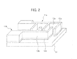
- the comb-shaped electrode may be exemplified by one in which a positive electrode and a negative electrode are each formed into a comb shape and oppositely disposed so that the parts of teeth of the comb shapes are alternately arranged. More specifically, the comb-shaped electrodes 11a and 11b shown in FIG. 2 may be exemplified.
- the comb-shaped electrodes 11a and 11b are simply explained with reference to FIG. 2 .
- the comb-shaped electrodes 11a and 11b are each formed into a comb shape and oppositely disposed so that the parts of teeth of the comb shapes are alternately arranged.
- the comb-shaped electrode 11a is a positive electrode and the comb-shaped electrode 11b is a negative electrode.
- Such a configuration of the comb-shaped electrodes 11a and 11b leads to a shorter distance between the electrodes and a constant electrolyte resistance, thus exchange of lithium ion can be effectively performed, thereby electric capacitance can be increased.
- the comb-shaped electrodes 11a and 11b are formed on the surface of the substrate 14 of which the surface is a non-conductor.
- a substrate 14 may be exemplified by silicon substrates having an oxide film on their surface.
- the comb-shaped electrode 11a of a positive electrode has the current collector 12a to draw a current and the positive-electrode active material layer 13a formed on the surface of the current collector 12a.
- the current collector 12a is formed into a comb shape in planar view.
- the positive-electrode active material layer 13a is formed on the surface of the comb-shaped current collector 12a and formed into a comb shape in planar view similarly to the current collector 12a.
- the current collector 12a is constructed from metal and preferably gold. Then, in order to ensure the adhesion between the current collector 12a and the substrate 14, an adhesion imparting layer (not shown) is formed between the current collector 12a and the substrate 14 as necessary.
- the adhesion imparting layer is appropriately set considering the material of the current collector 12a and the material of the substrate 14. As an example, when the current collector 2a is constructed from gold and the substrate 14 is constructed from silicon, a thin film of titanium is preferably used as the adhesion imparting layer.
- the thickness of the current collector 12a and the thickness of the adhesion imparting layer may be optionally set without particular limitation thereto. As an example, the thickness of the current collector 12a is 100 nm and the thickness of the adhesion imparting layer is 50 nm, without particular limitation thereto.
- the comb-shaped electrode 11b of a negative electrode has the current collector 12b to draw a current and the negative-electrode active material layer 13b formed on the surface of the current collector 12b.
- the other items of the comb-shaped electrode 11b are similar to those of the comb-shaped electrode 11a of a positive electrode; therefore, explanations thereof are omitted.
- An electrolyte (not shown) is provided between the comb-shaped electrode 11a of a positive electrode and the comb-shaped electrode 11b of a negative electrode. Consequently, the comb-shaped electrode 11a and the comb-shaped electrode 11b each cause an electrode reaction, and the current can be drawn from the current collector 12a and the current collector 12b.
- the entire size of comb-shaped electrodes; the thickness, length, and number of teeth in the comb-shaped electrode 11a or the comb-shaped electrode 11b; the space between two adjacent teeth; the thickness of active material layers, etc. may be appropriately adjusted depending on the desirable charged capacity and discharged capacity.
- 10 to 50 ⁇ m of the thickness of teeth, 30 to 70 ⁇ m of the space between two adjacent teeth, and 10 to 50 ⁇ m of the thickness of active material layers may be employed.
- the material to construct the positive-electrode active material layer 13a and the negative-electrode active material layer 13b and the type of the electrolyte may be appropriately set depending on the type of the cell to be formed.
- the material to construct the positive-electrode active material layer 13a may be exemplified by transition metal oxides such as lithium cobaltate
- the material to construct the negative-electrode active material layer 13b may be exemplified by carbon, graphite, lithium titanate, etc.
- the electrolyte may be exemplified by electrolyte liquids containing a salt such as lithium perchlorate and lithium hexafluorophosphate and an organic solvent in which the salt is soluble such as carbonate ester compounds including ethylene carbonate, dimethyl carbonate and diethyl carbonate, and acetonitrile, and mixtures of two or more of them, and gel-like electrolytes containing the above-mentioned electro
- the active material may be exemplified by particles of positive-electrode active materials such as LiCoO 2 , LiFePO 4 , and LiMn 2 O 4 and particles of negative-electrode active materials such as graphite, Li 4 Ti 5 O 12 , Sn alloys, and Si-based compounds.
- the active material is used in a condition of dispersion liquid where the active material is dispersed in a dispersion medium.
- the dispersion medium used may be exemplified by water, acetonitrile, N-methylpyrrolidone, acetone, ethanol, etc.
- the amount of the dispersion medium used is the amount that leads to 35 to 60 mass% of solid content concentration in the dispersion liquid.
- the dispersion liquid typically contains a binder such as styrene-butadiene rubber (SBR) and polyvinylidene fluoride.
- the dispersion liquid may also contain a conductive aid such as carbon black (e.g. acetylene black) and a dispersant such as carboxymethylcellulose.
- a conductive aid such as carbon black (e.g. acetylene black) and a dispersant such as carboxymethylcellulose.
- the contents of the active material, binder, conductive aid, and dispersant in the solid content of the dispersion liquid are not particularly limited.
- the content of the active material is preferably 85 to 99 mass%
- the content of the binder is preferably 1 to 15 mass%
- the content of the conductive aid is preferably 0 to 9 mass%
- the content of the dispersant is preferably 0 to 7 mass%.
- the content of the salt is adjusted such that the concentration of metal atom (e.g. lithium atom) constituting the salt is 0.2 to 2.0 M.
- the content of the polymer is 2 to 80 mass%.
- the above-mentioned electrolyte liquid may also contain an additive including unsaturated cyclic carbonate ester compounds such as vinylene carbonate, halogen-substituted carbonate ester compounds such as fluoroethylene carbonate, cyclic sulfonate-based compounds such as 1,3-propane sultone, cyclic sulfite ester compounds such as ethylene sulfite, crown ethers such as 12-crown-4, and aromatic compounds such as benzene and toluene.
- unsaturated cyclic carbonate ester compounds such as vinylene carbonate
- halogen-substituted carbonate ester compounds such as fluoroethylene carbonate
- cyclic sulfonate-based compounds such as 1,3-propane sultone
- cyclic sulfite ester compounds such as ethylene sulfite
- crown ethers such as 12-crown-4
- aromatic compounds such as benzene and toluen
- the comb-shaped electrodes 11a and 11b shown in FIG. 2 can be produced by forming a conductive layer on the surface of the substrate 14, patterning the conductive layer to form current collectors 12a and 12b, and forming a positive electrode and a negative electrode on the current collectors 12a and 12b using the pattern forming method according to the embodiment of the present invention explained with reference to FIGs. 1A to 1H , for example.
- the conductive layer and current collectors 12a and 12b can be formed by the method described in Patent Document 1, for example.
- the negative and positive electrodes can be formed on the current collectors 12a and 12b by forming a pattern in accordance with FIGs. 1A to 1H using the current collectors 12a and 12b of FIG. 2 as the support in FIGs.
- the resist composition 1 is novolac type, non-chemical amplification type, and positive type.
- the comb-shaped electrodes 11a and 11b shown in FIG. 2 were prepared using a screen printing process.
- an aluminum film (thickness: 200 nm) as a conductive layer was formed by a sputtering process on the surface of a silicon substrate having an oxide film.
- the positive-type resist composition 1 of Synthesis Example 1 was coated on the substrate by a spin coating process to thereby form a resist layer of 1.5 ⁇ m, followed by drying at 120°C for 1 minute.
- the resist layer was selectively exposed (ghi mixed rays, exposure amount: 100 mJ/cm 2 ) using a mask with a pattern corresponding to the comb-shaped electrodes 11a and 11b shown in FIG. 2 .
- development was carried out with an alkaline developer of 2.38 mass% TMAH for 1 minute.
- the resist composition of Synthesis Example 1 was coated by a spin coating process on a surface of silicon wafer on which the current collector had been formed, to thereby form a resist layer of 50 ⁇ m, followed by drying at 140°C for 5 minutes. Then, using a positive mask having the same shape in planar view as that of the above-formed comb-shaped current collector 12a, the resist layer at the position above the comb-shaped current collectors was exposed (ghi mixed rays, exposure amount: 60 mJ/cm 2 ). Next, baking was carried out at 85°C for 3 minutes as an activation step, followed by development with an alkaline developer. Consequently, a comb-shaped guide hole having the same shape in planar view as that of the current collector 12a was formed on the surface of the silicon wafer. The current collector 12a was exposed at the base of the guide hole.
- the screen printing was carried out on the silicon wafer where the guide hole had been formed and the positive-electrode active material was filled into the guide hole followed by drying at 100°C for 5 minutes, thereby forming a positive-electrode active material layer.
- the screen printing was carried out at a squeegee pressure of 180 MPa and a squeegee speed of 15.0 mm/sec using a screen printer (model MT-320T, manufactured by Micro-tec Co.) equipped with a silicon squeegee polished to an angle of 45° and having a hardness of 60°.
- the resist composition 2 of Synthesis Example 2 was coated by a spin coating process on a surface of silicon wafer on which the positive-electrode active material had been deposited to thereby form a resist layer of 10 ⁇ m, followed by drying at 140°C for 1 minute and formation of a protective layer.
- the resist layer at the position above the comb-shaped current collectors was exposed (ghi mixed rays, exposure amount: 60 mJ/cm 2 ).
- baking was carried out at 85°C for 3 minutes as an activation step, followed by development with an alkaline developer. Consequently, while protecting the positive-electrode active material by the protective layer, a comb-shaped guide hole having the same shape in planar view as that of the current collector 12b was formed on the surface of the silicon wafer. The current collector 12b was exposed at the base of the guide hole.
- the screen printing was carried out on the silicon wafer where the guide hole had been formed and the negative-electrode active material was filled into the guide hole followed by drying at 100°C for 5 minutes, thereby forming a negative-electrode active material layer.
- the screen printing was carried out at a squeegee pressure of 180 MPa and a squeegee speed of 15.0 mm/sec using a screen printer (model MT-320T, manufactured by Micro-tec Co.) equipped with a silicon squeegee polished to an angle of 45° and having a hardness of 60°.
- the resist layer was peeled off with acetone, thereby obtaining comb-shaped electrodes 11a and 11b.
- the time required for filling the electrode active materials by the screen printing process was as very short as 15 minutes.
- the comb-shaped electrodes 11a and 11b shown in FIG. 2 were prepared using an injection process.
- Comb-shaped current collectors 12a and 12b were formed similarly to Example 1.
- the resist composition of Synthesis Example 1 was coated by a spin coating process on a surface of silicon wafer on which the current collector had been formed to thereby form a resist layer of 50 ⁇ m, followed by drying at 140°C for 5 minutes. Then, using a positive mask having the same shape in planar view as that of the above-formed comb-shaped current collector, the resist layer at the position above the comb-shaped current collectors was exposed (ghi mixed rays, exposure amount: 60 mJ/cm 2 ). Next, baking was carried out at 85°C for 3 minutes as an activation step, followed by development with an alkaline developer. Consequently, a comb-shaped guide hole was formed on the surface of the silicon wafer. The current collector was exposed at the base of the guide hole.
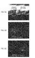
- FIG. 3A in regards to the comb-shaped electrodes 11a and 11b, it could be confirmed that the positive-electrode active material and the negative-electrode active material were filled with tracing the shape of guide holes without variation. Furthermore, as shown in FIG. 3B , existence of phosphorus was observed in the positive electrodes and thus filling of the positive-electrode active material could be confirmed. On the other hand, as shown in FIG. 3C , existence of titanium was observed in the negative electrodes and thus filling of the negative-electrode active material could be confirmed.
- the comb-shaped electrodes 11a and 11b shown in FIG. 2 were prepared similarly to Example 3 except that the mass ratio of LiFePO 4 particles, acetylene black, carboxymethylcellulose, and SBR was changed to 81:12:5:2 and the mass ratio of Li 4 Ti 5 O 12 particles, acetylene black, carboxymethylcellulose, and SBR was changed to 81:12:5:2.
- whisker-like residual dross of the positive-electrode active material or the negative-electrode active material does not appear and short circuit between electrodes can be prevented by way that the amount of acetylene black, a conductive aid, is reduced by half from 12 mass% to 6 mass% in the positive-electrode active material or the negative-electrode active material.
- the comb-shaped electrodes 11a and 11b shown in FIG. 2 were prepared similarly to Example 3 except that the entire size of comb-shaped electrodes, thickness of teeth, space between two adjacent teeth, length of teeth, number of teeth, and thickness of active material layers were set as shown in Table 1.
- the space between the resulting comb-shaped electrodes 11a and 11b was filled with an electrolyte liquid (1M LiClO 4 solution, solvent: mixture liquid of ethylene carbonate and diethyl carbonate of volume ratio 1:1) to thereby prepare secondary cells.
- an electrolyte liquid (1M LiClO 4 solution, solvent: mixture liquid of ethylene carbonate and diethyl carbonate of volume ratio 1:1
- Example 4 These secondary cells were charged and discharged with setting a current value to 20 ⁇ A (Example 4), 160 ⁇ A (Example 5), or 225 ⁇ A (Example 6).
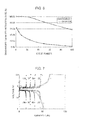
- the charge-discharge curves are shown in FIG. 4 .
- the values of discharged capacities read from the charge-discharge curves are also shown in Table 1. Note that the English characters A to C in FIG. 4 represent the comb-shaped electrodes A to C, respectively.
- Electrolyte liquid was prepared by mixing 3 parts by mass of polyethylene oxide with the mass average molecular weight of 80,000, 10 parts by mass of acetonitrile, and 7.2 parts by mass of 1M LiClO 4 solution (solvent: mixture liquid of ethylene carbonate and diethyl carbonate of volume ratio 1:1).
- the surface resistance of the gelled electrolyte formed as described above was measured to be 100 k ⁇ with a tester in the atmosphere in 3 minutes after the end of the drying.
- the impedance of the gelled electrolyte was measured as described below.
- a polyimide film with a diameter of 8 mm and with a thickness of 60 ⁇ m having a through-hole with a diameter of 5 mm was adhered tightly onto a Au substrate with a thickness of 2 mm.
- the electrolyte liquid containing polyethylene oxide was dropwise added into the concave part formed with the Au substrate and the through-hole and dried at 80°C for 20 minutes.
- Another Au substrate with a thickness of 2 mm was placed on the polyimide film and the formed gelled electrolyte. Voltage was applied between the two Au substrates under the conditions described below, and the impedance was measured to be 5.66 ⁇ 10 -4 Scm -1 .
- the comb-shaped electrodes 11a and 11b shown in FIG. 2 were prepared similarly to Example 3 except that the entire size of comb-shaped electrodes, thickness of teeth, space between two adjacent teeth, length of teeth, number of teeth, and thickness of active material layers were set as shown in Table 3.
- the electrolyte liquid containing polyethylene oxide was dropwise added into the space between the resulting comb-shaped electrodes 11a and 11b and dried at 80°C for 20 minutes. Thereby, secondary cells in which the space was filled with the gelled electrolyte were prepared. These secondary cells were charged and discharged with setting a current value to 50 ⁇ A. Charging and discharging were repeated for 100 cycles, and the charged capacities and discharged capacities at 1, 25, 50, 75, and 100 cycles were measured.
- the secondary cells with the comb-shaped electrode produced by the pattern forming method according to the present invention have a good charge-discharge property even when a gelled electrolyte were used.
- Example 4 Regarding the comb-shaped electrode prepared in Example 4, charging and discharging were performed similarly to Example 4 with a C-rate set to 1C, 2C, 5C, 10C, 20C, or 40C. The charge-discharge curves are shown in FIG. 8 . The discharged capacity retention rate at each C-rate is shown in Table 4 with the discharged capacity at 1C set to 100%. [Table 4] C-rate 1 2 5 10 20 40 Discharged Capacity Retention Rate (%) 100 100 100 100 94 83 69
- the secondary cells with the comb-shaped electrode produced by the pattern forming method according to the present invention have a good discharged capacity retention rate even when the C-rate increases, and have an equal performance to the secondary cells with the comb-shaped electrode produced by the injection process.
- Example 4 Regarding the comb-shaped electrode prepared in Example 4, charging and discharging were performed similarly to Example 4. Charging and discharging were repeated for 250 cycles, and the charged capacities and discharged capacities were measured at predetermined cycles. The capacity retention rate at each cycle is shown in FIG. 9A with the charged capacity and the discharged capacity at 1 cycle set to 100%. The coulomb efficiency (namely, discharged capacity/charged capacity) at each cycle is shown in FIG. 9B .
- the secondary cells with the comb-shaped electrode produced by the pattern forming method according to the present invention have a stable capacity retention rate and retain a coulomb efficiency at a high value of 98.8%.
Landscapes
- Chemical & Material Sciences (AREA)
- Engineering & Computer Science (AREA)
- Chemical Kinetics & Catalysis (AREA)
- General Chemical & Material Sciences (AREA)
- Electrochemistry (AREA)
- Manufacturing & Machinery (AREA)
- Materials Engineering (AREA)
- Physics & Mathematics (AREA)
- General Physics & Mathematics (AREA)
- Battery Electrode And Active Subsutance (AREA)
- Materials For Photolithography (AREA)
- Photosensitive Polymer And Photoresist Processing (AREA)
- Cell Electrode Carriers And Collectors (AREA)
Applications Claiming Priority (3)
| Application Number | Priority Date | Filing Date | Title |
|---|---|---|---|
| JP2012197802 | 2012-09-07 | ||
| JP2013026856A JP6174331B2 (ja) | 2012-09-07 | 2013-02-14 | パターン形成方法、構造体、櫛型電極の製造方法、及び二次電池 |
| PCT/JP2013/073058 WO2014038454A1 (ja) | 2012-09-07 | 2013-08-28 | パターン形成方法、構造体、櫛型電極の製造方法、及び二次電池 |
Publications (3)
| Publication Number | Publication Date |
|---|---|
| EP2894697A1 true EP2894697A1 (de) | 2015-07-15 |
| EP2894697A4 EP2894697A4 (de) | 2015-08-19 |
| EP2894697B1 EP2894697B1 (de) | 2017-05-03 |
Family
ID=50237066
Family Applications (1)
| Application Number | Title | Priority Date | Filing Date |
|---|---|---|---|
| EP13835967.4A Not-in-force EP2894697B1 (de) | 2012-09-07 | 2013-08-28 | Strukturformungsverfahren und verfahren zur herstellung ineinandergreifender elektroden |
Country Status (6)
| Country | Link |
|---|---|
| US (1) | US9478791B2 (de) |
| EP (1) | EP2894697B1 (de) |
| JP (1) | JP6174331B2 (de) |
| KR (1) | KR101645904B1 (de) |
| TW (1) | TWI605630B (de) |
| WO (1) | WO2014038454A1 (de) |
Families Citing this family (6)
| Publication number | Priority date | Publication date | Assignee | Title |
|---|---|---|---|---|
| US11527774B2 (en) | 2011-06-29 | 2022-12-13 | Space Charge, LLC | Electrochemical energy storage devices |
| US11996517B2 (en) | 2011-06-29 | 2024-05-28 | Space Charge, LLC | Electrochemical energy storage devices |
| JP6150587B2 (ja) * | 2013-03-29 | 2017-06-21 | 東京応化工業株式会社 | パターン形成方法、構造体、櫛型電極の製造方法、及び二次電池 |
| US10593945B2 (en) * | 2017-03-20 | 2020-03-17 | Bing R. Hsieh | Printed planar lithium-ion batteries |
| EP3762989A4 (de) * | 2018-03-07 | 2021-12-15 | Space Charge, LLC | Dünnfilm-festkörper-energiespeichervorrichtungen |
| KR102875786B1 (ko) | 2020-07-15 | 2025-10-23 | 에스케이온 주식회사 | 이차전지용 전극 |
Family Cites Families (14)
| Publication number | Priority date | Publication date | Assignee | Title |
|---|---|---|---|---|
| DE4108986A1 (de) | 1990-03-19 | 1991-09-26 | Hitachi Ltd | Zusammengeschaltete, mehrschichtige platten und verfahren zu ihrer herstellung |
| JP2968349B2 (ja) * | 1991-02-01 | 1999-10-25 | 日本ペイント株式会社 | 多色表示装置の製造方法 |
| JPH10228864A (ja) * | 1997-02-14 | 1998-08-25 | Dainippon Printing Co Ltd | プラズマディスプレイパネルの背面板の製造方法及び背面板形成用組成物 |
| US6106992A (en) | 1996-11-14 | 2000-08-22 | Dai Nippon Printing Co., Ltd. | Photoresist film and process for producing back plate of plasma display panel |
| JP3877449B2 (ja) * | 1998-10-07 | 2007-02-07 | ナミックス株式会社 | 蛍光体パターンの形成方法 |
| JP2000123729A (ja) * | 1998-10-12 | 2000-04-28 | Dainippon Printing Co Ltd | プラズマディスプレイパネルの蛍光面形成方法 |
| JP3700460B2 (ja) | 1999-04-05 | 2005-09-28 | セイコーエプソン株式会社 | 半導体装置およびその製造方法 |
| JP2001144128A (ja) * | 1999-11-15 | 2001-05-25 | Ebara Corp | 導電体の印刷方法 |
| JP2003068667A (ja) * | 2001-08-29 | 2003-03-07 | Umc Japan | 半導体装置の製造方法 |
| JP3818188B2 (ja) | 2002-03-22 | 2006-09-06 | Tdk株式会社 | マスクパターンの形成方法、該マスクパターンを用いたパターニング方法及び薄膜磁気ヘッドの製造方法 |
| FR2880197B1 (fr) | 2004-12-23 | 2007-02-02 | Commissariat Energie Atomique | Electrolyte structure pour microbatterie |
| JP5158370B2 (ja) | 2008-02-14 | 2013-03-06 | 信越化学工業株式会社 | ダブルパターン形成方法 |
| JP5695928B2 (ja) * | 2010-04-14 | 2015-04-08 | 東京応化工業株式会社 | 櫛型電極の製造方法 |
| JP2012023418A (ja) * | 2010-07-12 | 2012-02-02 | Murata Mfg Co Ltd | 電子部品の製造方法 |
-
2013
- 2013-02-14 JP JP2013026856A patent/JP6174331B2/ja not_active Expired - Fee Related
- 2013-08-28 EP EP13835967.4A patent/EP2894697B1/de not_active Not-in-force
- 2013-08-28 KR KR1020157008038A patent/KR101645904B1/ko not_active Expired - Fee Related
- 2013-08-28 US US14/426,300 patent/US9478791B2/en active Active
- 2013-08-28 WO PCT/JP2013/073058 patent/WO2014038454A1/ja not_active Ceased
- 2013-09-04 TW TW102131783A patent/TWI605630B/zh active
Also Published As
| Publication number | Publication date |
|---|---|
| TWI605630B (zh) | 2017-11-11 |
| KR20150043517A (ko) | 2015-04-22 |
| US20150243965A1 (en) | 2015-08-27 |
| EP2894697A4 (de) | 2015-08-19 |
| JP6174331B2 (ja) | 2017-08-02 |
| US9478791B2 (en) | 2016-10-25 |
| TW201424094A (zh) | 2014-06-16 |
| EP2894697B1 (de) | 2017-05-03 |
| KR101645904B1 (ko) | 2016-08-04 |
| JP2014066992A (ja) | 2014-04-17 |
| WO2014038454A1 (ja) | 2014-03-13 |
Similar Documents
| Publication | Publication Date | Title |
|---|---|---|
| EP3012897B1 (de) | Sekundärbatterie mit nichtwässrigem elektrolyten und verfahren zur herstellung davon | |
| JP6604532B2 (ja) | 非水二次電池、その製造方法、及び電解質 | |
| EP2894697B1 (de) | Strukturformungsverfahren und verfahren zur herstellung ineinandergreifender elektroden | |
| US20240347763A1 (en) | Glass solid electrolyte layer, methods of making glass solid electrolyte layer and electrodes and battery cells thereof | |
| EP2784585B1 (de) | Verfahren zur Herstellung eines Musters, Bauteil, Verfahren zur Herstellung einer kammförmigen Elektrode, und Sekundärzelle | |
| KR20150058303A (ko) | 에너지 저장 디바이스 전극용 복합 집전체 및 전극 | |
| Nakano et al. | All-solid-state micro lithium-ion batteries fabricated by using dry polymer electrolyte with micro-phase separation structure | |
| US10566617B2 (en) | Microbattery | |
| JP7050944B2 (ja) | リチウム電極及びこれを含むリチウム二次電池 | |
| US9196897B2 (en) | Secondary battery porous electrode | |
| JP2008543025A (ja) | リチウム再充電可能電気化学セル | |
| US11063261B2 (en) | Electrode for electrochemical device, method for manufacturing the same, and electrochemical device including the same | |
| US20240194854A1 (en) | Rechargeable anode-free sodium metal batteries enabled by non-porous sodium metal plating and stripping | |
| CN110911647A (zh) | 制造锂离子单池的方法 | |
| KR101458212B1 (ko) | 독립된 분리막을 포함하지 않는 이차전지 | |
| Neidhart | Manufacturing of high-loading aqueous cathodes for Li-ion batteries |
Legal Events
| Date | Code | Title | Description |
|---|---|---|---|
| PUAI | Public reference made under article 153(3) epc to a published international application that has entered the european phase |
Free format text: ORIGINAL CODE: 0009012 |
|
| 17P | Request for examination filed |
Effective date: 20150402 |
|
| AK | Designated contracting states |
Kind code of ref document: A1 Designated state(s): AL AT BE BG CH CY CZ DE DK EE ES FI FR GB GR HR HU IE IS IT LI LT LU LV MC MK MT NL NO PL PT RO RS SE SI SK SM TR |
|
| AX | Request for extension of the european patent |
Extension state: BA ME |
|
| RA4 | Supplementary search report drawn up and despatched (corrected) |
Effective date: 20150716 |
|
| RIC1 | Information provided on ipc code assigned before grant |
Ipc: H01M 4/70 20060101ALI20150710BHEP Ipc: H01L 21/288 20060101ALI20150710BHEP Ipc: H01M 6/40 20060101ALI20150710BHEP Ipc: G03F 7/00 20060101ALI20150710BHEP Ipc: H01L 21/768 20060101ALI20150710BHEP Ipc: G03F 7/40 20060101ALI20150710BHEP Ipc: H01M 4/04 20060101ALI20150710BHEP Ipc: H01M 4/139 20100101ALI20150710BHEP Ipc: H01M 4/13 20100101AFI20150710BHEP Ipc: G03F 7/12 20060101ALI20150710BHEP Ipc: H01M 4/02 20060101ALN20150710BHEP Ipc: H01M 10/0565 20100101ALN20150710BHEP Ipc: H01M 10/052 20100101ALN20150710BHEP Ipc: H01M 10/058 20100101ALI20150710BHEP |
|
| DAX | Request for extension of the european patent (deleted) | ||
| 17Q | First examination report despatched |
Effective date: 20160517 |
|
| GRAP | Despatch of communication of intention to grant a patent |
Free format text: ORIGINAL CODE: EPIDOSNIGR1 |
|
| STAA | Information on the status of an ep patent application or granted ep patent |
Free format text: STATUS: GRANT OF PATENT IS INTENDED |
|
| RIC1 | Information provided on ipc code assigned before grant |
Ipc: H01M 4/70 20060101ALI20161123BHEP Ipc: G03F 7/40 20060101ALI20161123BHEP Ipc: G03F 7/00 20060101ALI20161123BHEP Ipc: H01M 10/052 20100101ALN20161123BHEP Ipc: H01M 10/0565 20100101ALN20161123BHEP Ipc: H01M 10/058 20100101ALI20161123BHEP Ipc: G03F 7/12 20060101ALI20161123BHEP Ipc: H01M 6/40 20060101ALI20161123BHEP Ipc: H01M 4/04 20060101ALI20161123BHEP Ipc: H01M 4/02 20060101ALN20161123BHEP Ipc: H01M 4/13 20100101AFI20161123BHEP Ipc: H01L 21/288 20060101ALI20161123BHEP Ipc: H01L 21/768 20060101ALI20161123BHEP Ipc: H01M 4/139 20100101ALI20161123BHEP |
|
| INTG | Intention to grant announced |
Effective date: 20161214 |
|
| GRAS | Grant fee paid |
Free format text: ORIGINAL CODE: EPIDOSNIGR3 |
|
| GRAA | (expected) grant |
Free format text: ORIGINAL CODE: 0009210 |
|
| STAA | Information on the status of an ep patent application or granted ep patent |
Free format text: STATUS: THE PATENT HAS BEEN GRANTED |
|
| AK | Designated contracting states |
Kind code of ref document: B1 Designated state(s): AL AT BE BG CH CY CZ DE DK EE ES FI FR GB GR HR HU IE IS IT LI LT LU LV MC MK MT NL NO PL PT RO RS SE SI SK SM TR |
|
| REG | Reference to a national code |
Ref country code: GB Ref legal event code: FG4D |
|
| REG | Reference to a national code |
Ref country code: AT Ref legal event code: REF Ref document number: 890899 Country of ref document: AT Kind code of ref document: T Effective date: 20170515 Ref country code: CH Ref legal event code: EP |
|
| REG | Reference to a national code |
Ref country code: IE Ref legal event code: FG4D |
|
| REG | Reference to a national code |
Ref country code: DE Ref legal event code: R096 Ref document number: 602013020792 Country of ref document: DE |
|
| REG | Reference to a national code |
Ref country code: FR Ref legal event code: PLFP Year of fee payment: 5 |
|
| REG | Reference to a national code |
Ref country code: NL Ref legal event code: MP Effective date: 20170503 |
|
| REG | Reference to a national code |
Ref country code: AT Ref legal event code: MK05 Ref document number: 890899 Country of ref document: AT Kind code of ref document: T Effective date: 20170503 |
|
| REG | Reference to a national code |
Ref country code: LT Ref legal event code: MG4D |
|
| PG25 | Lapsed in a contracting state [announced via postgrant information from national office to epo] |
Ref country code: FI Free format text: LAPSE BECAUSE OF FAILURE TO SUBMIT A TRANSLATION OF THE DESCRIPTION OR TO PAY THE FEE WITHIN THE PRESCRIBED TIME-LIMIT Effective date: 20170503 Ref country code: HR Free format text: LAPSE BECAUSE OF FAILURE TO SUBMIT A TRANSLATION OF THE DESCRIPTION OR TO PAY THE FEE WITHIN THE PRESCRIBED TIME-LIMIT Effective date: 20170503 Ref country code: GR Free format text: LAPSE BECAUSE OF FAILURE TO SUBMIT A TRANSLATION OF THE DESCRIPTION OR TO PAY THE FEE WITHIN THE PRESCRIBED TIME-LIMIT Effective date: 20170804 Ref country code: LT Free format text: LAPSE BECAUSE OF FAILURE TO SUBMIT A TRANSLATION OF THE DESCRIPTION OR TO PAY THE FEE WITHIN THE PRESCRIBED TIME-LIMIT Effective date: 20170503 Ref country code: NO Free format text: LAPSE BECAUSE OF FAILURE TO SUBMIT A TRANSLATION OF THE DESCRIPTION OR TO PAY THE FEE WITHIN THE PRESCRIBED TIME-LIMIT Effective date: 20170803 Ref country code: ES Free format text: LAPSE BECAUSE OF FAILURE TO SUBMIT A TRANSLATION OF THE DESCRIPTION OR TO PAY THE FEE WITHIN THE PRESCRIBED TIME-LIMIT Effective date: 20170503 Ref country code: AT Free format text: LAPSE BECAUSE OF FAILURE TO SUBMIT A TRANSLATION OF THE DESCRIPTION OR TO PAY THE FEE WITHIN THE PRESCRIBED TIME-LIMIT Effective date: 20170503 |
|
| PG25 | Lapsed in a contracting state [announced via postgrant information from national office to epo] |
Ref country code: RS Free format text: LAPSE BECAUSE OF FAILURE TO SUBMIT A TRANSLATION OF THE DESCRIPTION OR TO PAY THE FEE WITHIN THE PRESCRIBED TIME-LIMIT Effective date: 20170503 Ref country code: SE Free format text: LAPSE BECAUSE OF FAILURE TO SUBMIT A TRANSLATION OF THE DESCRIPTION OR TO PAY THE FEE WITHIN THE PRESCRIBED TIME-LIMIT Effective date: 20170503 Ref country code: BG Free format text: LAPSE BECAUSE OF FAILURE TO SUBMIT A TRANSLATION OF THE DESCRIPTION OR TO PAY THE FEE WITHIN THE PRESCRIBED TIME-LIMIT Effective date: 20170803 Ref country code: NL Free format text: LAPSE BECAUSE OF FAILURE TO SUBMIT A TRANSLATION OF THE DESCRIPTION OR TO PAY THE FEE WITHIN THE PRESCRIBED TIME-LIMIT Effective date: 20170503 Ref country code: IS Free format text: LAPSE BECAUSE OF FAILURE TO SUBMIT A TRANSLATION OF THE DESCRIPTION OR TO PAY THE FEE WITHIN THE PRESCRIBED TIME-LIMIT Effective date: 20170903 Ref country code: LV Free format text: LAPSE BECAUSE OF FAILURE TO SUBMIT A TRANSLATION OF THE DESCRIPTION OR TO PAY THE FEE WITHIN THE PRESCRIBED TIME-LIMIT Effective date: 20170503 Ref country code: PL Free format text: LAPSE BECAUSE OF FAILURE TO SUBMIT A TRANSLATION OF THE DESCRIPTION OR TO PAY THE FEE WITHIN THE PRESCRIBED TIME-LIMIT Effective date: 20170503 |
|
| PG25 | Lapsed in a contracting state [announced via postgrant information from national office to epo] |
Ref country code: SK Free format text: LAPSE BECAUSE OF FAILURE TO SUBMIT A TRANSLATION OF THE DESCRIPTION OR TO PAY THE FEE WITHIN THE PRESCRIBED TIME-LIMIT Effective date: 20170503 Ref country code: EE Free format text: LAPSE BECAUSE OF FAILURE TO SUBMIT A TRANSLATION OF THE DESCRIPTION OR TO PAY THE FEE WITHIN THE PRESCRIBED TIME-LIMIT Effective date: 20170503 Ref country code: RO Free format text: LAPSE BECAUSE OF FAILURE TO SUBMIT A TRANSLATION OF THE DESCRIPTION OR TO PAY THE FEE WITHIN THE PRESCRIBED TIME-LIMIT Effective date: 20170503 Ref country code: DK Free format text: LAPSE BECAUSE OF FAILURE TO SUBMIT A TRANSLATION OF THE DESCRIPTION OR TO PAY THE FEE WITHIN THE PRESCRIBED TIME-LIMIT Effective date: 20170503 Ref country code: CZ Free format text: LAPSE BECAUSE OF FAILURE TO SUBMIT A TRANSLATION OF THE DESCRIPTION OR TO PAY THE FEE WITHIN THE PRESCRIBED TIME-LIMIT Effective date: 20170503 |
|
| REG | Reference to a national code |
Ref country code: DE Ref legal event code: R097 Ref document number: 602013020792 Country of ref document: DE |
|
| PG25 | Lapsed in a contracting state [announced via postgrant information from national office to epo] |
Ref country code: SM Free format text: LAPSE BECAUSE OF FAILURE TO SUBMIT A TRANSLATION OF THE DESCRIPTION OR TO PAY THE FEE WITHIN THE PRESCRIBED TIME-LIMIT Effective date: 20170503 Ref country code: IT Free format text: LAPSE BECAUSE OF FAILURE TO SUBMIT A TRANSLATION OF THE DESCRIPTION OR TO PAY THE FEE WITHIN THE PRESCRIBED TIME-LIMIT Effective date: 20170503 |
|
| PLBE | No opposition filed within time limit |
Free format text: ORIGINAL CODE: 0009261 |
|
| STAA | Information on the status of an ep patent application or granted ep patent |
Free format text: STATUS: NO OPPOSITION FILED WITHIN TIME LIMIT |
|
| REG | Reference to a national code |
Ref country code: CH Ref legal event code: PL |
|
| PG25 | Lapsed in a contracting state [announced via postgrant information from national office to epo] |
Ref country code: MC Free format text: LAPSE BECAUSE OF FAILURE TO SUBMIT A TRANSLATION OF THE DESCRIPTION OR TO PAY THE FEE WITHIN THE PRESCRIBED TIME-LIMIT Effective date: 20170503 |
|
| 26N | No opposition filed |
Effective date: 20180206 |
|
| GBPC | Gb: european patent ceased through non-payment of renewal fee |
Effective date: 20170828 |
|
| PG25 | Lapsed in a contracting state [announced via postgrant information from national office to epo] |
Ref country code: CH Free format text: LAPSE BECAUSE OF NON-PAYMENT OF DUE FEES Effective date: 20170831 Ref country code: LI Free format text: LAPSE BECAUSE OF NON-PAYMENT OF DUE FEES Effective date: 20170831 |
|
| REG | Reference to a national code |
Ref country code: IE Ref legal event code: MM4A |
|
| PG25 | Lapsed in a contracting state [announced via postgrant information from national office to epo] |
Ref country code: SI Free format text: LAPSE BECAUSE OF FAILURE TO SUBMIT A TRANSLATION OF THE DESCRIPTION OR TO PAY THE FEE WITHIN THE PRESCRIBED TIME-LIMIT Effective date: 20170503 |
|
| REG | Reference to a national code |
Ref country code: BE Ref legal event code: MM Effective date: 20170831 |
|
| PG25 | Lapsed in a contracting state [announced via postgrant information from national office to epo] |
Ref country code: LU Free format text: LAPSE BECAUSE OF NON-PAYMENT OF DUE FEES Effective date: 20170828 |
|
| REG | Reference to a national code |
Ref country code: FR Ref legal event code: PLFP Year of fee payment: 6 |
|
| PG25 | Lapsed in a contracting state [announced via postgrant information from national office to epo] |
Ref country code: GB Free format text: LAPSE BECAUSE OF NON-PAYMENT OF DUE FEES Effective date: 20170828 Ref country code: IE Free format text: LAPSE BECAUSE OF NON-PAYMENT OF DUE FEES Effective date: 20170828 |
|
| PG25 | Lapsed in a contracting state [announced via postgrant information from national office to epo] |
Ref country code: BE Free format text: LAPSE BECAUSE OF NON-PAYMENT OF DUE FEES Effective date: 20170831 |
|
| PG25 | Lapsed in a contracting state [announced via postgrant information from national office to epo] |
Ref country code: MT Free format text: LAPSE BECAUSE OF NON-PAYMENT OF DUE FEES Effective date: 20170828 |
|
| PG25 | Lapsed in a contracting state [announced via postgrant information from national office to epo] |
Ref country code: HU Free format text: LAPSE BECAUSE OF FAILURE TO SUBMIT A TRANSLATION OF THE DESCRIPTION OR TO PAY THE FEE WITHIN THE PRESCRIBED TIME-LIMIT; INVALID AB INITIO Effective date: 20130828 |
|
| PG25 | Lapsed in a contracting state [announced via postgrant information from national office to epo] |
Ref country code: CY Free format text: LAPSE BECAUSE OF FAILURE TO SUBMIT A TRANSLATION OF THE DESCRIPTION OR TO PAY THE FEE WITHIN THE PRESCRIBED TIME-LIMIT Effective date: 20170503 |
|
| PG25 | Lapsed in a contracting state [announced via postgrant information from national office to epo] |
Ref country code: MK Free format text: LAPSE BECAUSE OF FAILURE TO SUBMIT A TRANSLATION OF THE DESCRIPTION OR TO PAY THE FEE WITHIN THE PRESCRIBED TIME-LIMIT Effective date: 20170503 |
|
| PG25 | Lapsed in a contracting state [announced via postgrant information from national office to epo] |
Ref country code: TR Free format text: LAPSE BECAUSE OF FAILURE TO SUBMIT A TRANSLATION OF THE DESCRIPTION OR TO PAY THE FEE WITHIN THE PRESCRIBED TIME-LIMIT Effective date: 20170503 |
|
| PG25 | Lapsed in a contracting state [announced via postgrant information from national office to epo] |
Ref country code: PT Free format text: LAPSE BECAUSE OF FAILURE TO SUBMIT A TRANSLATION OF THE DESCRIPTION OR TO PAY THE FEE WITHIN THE PRESCRIBED TIME-LIMIT Effective date: 20170503 |
|
| PG25 | Lapsed in a contracting state [announced via postgrant information from national office to epo] |
Ref country code: AL Free format text: LAPSE BECAUSE OF FAILURE TO SUBMIT A TRANSLATION OF THE DESCRIPTION OR TO PAY THE FEE WITHIN THE PRESCRIBED TIME-LIMIT Effective date: 20170503 |
|
| PGFP | Annual fee paid to national office [announced via postgrant information from national office to epo] |
Ref country code: DE Payment date: 20240702 Year of fee payment: 12 |
|
| PGFP | Annual fee paid to national office [announced via postgrant information from national office to epo] |
Ref country code: FR Payment date: 20240702 Year of fee payment: 12 |
|
| REG | Reference to a national code |
Ref country code: DE Ref legal event code: R119 Ref document number: 602013020792 Country of ref document: DE |
|
| PG25 | Lapsed in a contracting state [announced via postgrant information from national office to epo] |
Ref country code: DE Free format text: LAPSE BECAUSE OF NON-PAYMENT OF DUE FEES Effective date: 20260303 |
|
| PG25 | Lapsed in a contracting state [announced via postgrant information from national office to epo] |
Ref country code: FR Free format text: LAPSE BECAUSE OF NON-PAYMENT OF DUE FEES Effective date: 20250831 |