EP2899245A1 - Anisotropes und leitfähiges haftmittel - Google Patents
Anisotropes und leitfähiges haftmittel Download PDFInfo
- Publication number
- EP2899245A1 EP2899245A1 EP13840056.9A EP13840056A EP2899245A1 EP 2899245 A1 EP2899245 A1 EP 2899245A1 EP 13840056 A EP13840056 A EP 13840056A EP 2899245 A1 EP2899245 A1 EP 2899245A1
- Authority
- EP
- European Patent Office
- Prior art keywords
- particles
- conductive
- anisotropic conductive
- solder
- conductive adhesive
- Prior art date
- Legal status (The legal status is an assumption and is not a legal conclusion. Google has not performed a legal analysis and makes no representation as to the accuracy of the status listed.)
- Granted
Links
Images


Classifications
-
- B—PERFORMING OPERATIONS; TRANSPORTING
- B23—MACHINE TOOLS; METAL-WORKING NOT OTHERWISE PROVIDED FOR
- B23K—SOLDERING OR UNSOLDERING; WELDING; CLADDING OR PLATING BY SOLDERING OR WELDING; CUTTING BY APPLYING HEAT LOCALLY, e.g. FLAME CUTTING; WORKING BY LASER BEAM
- B23K35/00—Rods, electrodes, materials, or media, for use in soldering, welding, or cutting
- B23K35/22—Rods, electrodes, materials, or media, for use in soldering, welding, or cutting characterised by the composition or nature of the material
- B23K35/36—Selection of non-metallic compositions, e.g. coatings or fluxes; Selection of soldering or welding materials, conjoint with selection of non-metallic compositions, both selections being of interest
-
- B—PERFORMING OPERATIONS; TRANSPORTING
- B23—MACHINE TOOLS; METAL-WORKING NOT OTHERWISE PROVIDED FOR
- B23K—SOLDERING OR UNSOLDERING; WELDING; CLADDING OR PLATING BY SOLDERING OR WELDING; CUTTING BY APPLYING HEAT LOCALLY, e.g. FLAME CUTTING; WORKING BY LASER BEAM
- B23K1/00—Soldering, e.g. brazing, or unsoldering
- B23K1/0008—Soldering, e.g. brazing, or unsoldering specially adapted for particular articles or work
- B23K1/0016—Soldering of electronic components
-
- B—PERFORMING OPERATIONS; TRANSPORTING
- B23—MACHINE TOOLS; METAL-WORKING NOT OTHERWISE PROVIDED FOR
- B23K—SOLDERING OR UNSOLDERING; WELDING; CLADDING OR PLATING BY SOLDERING OR WELDING; CUTTING BY APPLYING HEAT LOCALLY, e.g. FLAME CUTTING; WORKING BY LASER BEAM
- B23K35/00—Rods, electrodes, materials, or media, for use in soldering, welding, or cutting
- B23K35/02—Rods, electrodes, materials, or media, for use in soldering, welding, or cutting characterised by mechanical features, e.g. shape
- B23K35/0222—Rods, electrodes, materials, or media, for use in soldering, welding, or cutting characterised by mechanical features, e.g. shape for use in soldering or brazing
- B23K35/0244—Powders, particles or spheres; Preforms made therefrom
- B23K35/025—Pastes, creams or slurries
-
- B—PERFORMING OPERATIONS; TRANSPORTING
- B23—MACHINE TOOLS; METAL-WORKING NOT OTHERWISE PROVIDED FOR
- B23K—SOLDERING OR UNSOLDERING; WELDING; CLADDING OR PLATING BY SOLDERING OR WELDING; CUTTING BY APPLYING HEAT LOCALLY, e.g. FLAME CUTTING; WORKING BY LASER BEAM
- B23K35/00—Rods, electrodes, materials, or media, for use in soldering, welding, or cutting
- B23K35/22—Rods, electrodes, materials, or media, for use in soldering, welding, or cutting characterised by the composition or nature of the material
- B23K35/24—Selection of soldering or welding materials proper
-
- C—CHEMISTRY; METALLURGY
- C09—DYES; PAINTS; POLISHES; NATURAL RESINS; ADHESIVES; COMPOSITIONS NOT OTHERWISE PROVIDED FOR; APPLICATIONS OF MATERIALS NOT OTHERWISE PROVIDED FOR
- C09J—ADHESIVES; NON-MECHANICAL ASPECTS OF ADHESIVE PROCESSES IN GENERAL; ADHESIVE PROCESSES NOT PROVIDED FOR ELSEWHERE; USE OF MATERIALS AS ADHESIVES
- C09J11/00—Features of adhesives not provided for in group C09J9/00, e.g. additives
-
- C—CHEMISTRY; METALLURGY
- C09—DYES; PAINTS; POLISHES; NATURAL RESINS; ADHESIVES; COMPOSITIONS NOT OTHERWISE PROVIDED FOR; APPLICATIONS OF MATERIALS NOT OTHERWISE PROVIDED FOR
- C09J—ADHESIVES; NON-MECHANICAL ASPECTS OF ADHESIVE PROCESSES IN GENERAL; ADHESIVE PROCESSES NOT PROVIDED FOR ELSEWHERE; USE OF MATERIALS AS ADHESIVES
- C09J9/00—Adhesives characterised by their physical nature or the effects produced, e.g. glue sticks
- C09J9/02—Electrically-conducting adhesives
-
- H—ELECTRICITY
- H01—ELECTRIC ELEMENTS
- H01B—CABLES; CONDUCTORS; INSULATORS; SELECTION OF MATERIALS FOR THEIR CONDUCTIVE, INSULATING OR DIELECTRIC PROPERTIES
- H01B1/00—Conductors or conductive bodies characterised by the conductive materials; Selection of materials as conductors
- H01B1/20—Conductive material dispersed in non-conductive organic material
- H01B1/22—Conductive material dispersed in non-conductive organic material the conductive material comprising metals or alloys
-
- H—ELECTRICITY
- H05—ELECTRIC TECHNIQUES NOT OTHERWISE PROVIDED FOR
- H05K—PRINTED CIRCUITS; CASINGS OR CONSTRUCTIONAL DETAILS OF ELECTRIC APPARATUS; MANUFACTURE OF ASSEMBLAGES OF ELECTRICAL COMPONENTS
- H05K13/00—Apparatus or processes specially adapted for manufacturing or adjusting assemblages of electric components
- H05K13/04—Mounting of components, e.g. of leadless components
- H05K13/046—Surface mounting
- H05K13/0465—Surface mounting by soldering
-
- H—ELECTRICITY
- H05—ELECTRIC TECHNIQUES NOT OTHERWISE PROVIDED FOR
- H05K—PRINTED CIRCUITS; CASINGS OR CONSTRUCTIONAL DETAILS OF ELECTRIC APPARATUS; MANUFACTURE OF ASSEMBLAGES OF ELECTRICAL COMPONENTS
- H05K3/00—Apparatus or processes for manufacturing printed circuits
- H05K3/30—Assembling printed circuits with electric components, e.g. with resistors
- H05K3/32—Assembling printed circuits with electric components, e.g. with resistors electrically connecting electric components or wires to printed circuits
- H05K3/34—Assembling printed circuits with electric components, e.g. with resistors electrically connecting electric components or wires to printed circuits by soldering
- H05K3/3465—Application of solder
- H05K3/3485—Application of solder paste, slurry or powder
-
- H—ELECTRICITY
- H10—SEMICONDUCTOR DEVICES; ELECTRIC SOLID-STATE DEVICES NOT OTHERWISE PROVIDED FOR
- H10H—INORGANIC LIGHT-EMITTING SEMICONDUCTOR DEVICES HAVING POTENTIAL BARRIERS
- H10H20/00—Individual inorganic light-emitting semiconductor devices having potential barriers, e.g. light-emitting diodes [LED]
- H10H20/80—Constructional details
- H10H20/85—Packages
- H10H20/857—Interconnections, e.g. lead-frames, bond wires or solder balls
-
- H—ELECTRICITY
- H10—SEMICONDUCTOR DEVICES; ELECTRIC SOLID-STATE DEVICES NOT OTHERWISE PROVIDED FOR
- H10W—GENERIC PACKAGES, INTERCONNECTIONS, CONNECTORS OR OTHER CONSTRUCTIONAL DETAILS OF DEVICES COVERED BY CLASS H10
- H10W20/00—Interconnections in chips, wafers or substrates
- H10W20/40—Interconnections external to wafers or substrates, e.g. back-end-of-line [BEOL] metallisations or vias connecting to gate electrodes
- H10W20/41—Interconnections external to wafers or substrates, e.g. back-end-of-line [BEOL] metallisations or vias connecting to gate electrodes characterised by their conductive parts
- H10W20/44—Conductive materials thereof
- H10W20/4473—Conductive organic materials, e.g. conductive adhesives or conductive inks
-
- C—CHEMISTRY; METALLURGY
- C08—ORGANIC MACROMOLECULAR COMPOUNDS; THEIR PREPARATION OR CHEMICAL WORKING-UP; COMPOSITIONS BASED THEREON
- C08K—Use of inorganic or non-macromolecular organic substances as compounding ingredients
- C08K2201/00—Specific properties of additives
- C08K2201/001—Conductive additives
-
- C—CHEMISTRY; METALLURGY
- C08—ORGANIC MACROMOLECULAR COMPOUNDS; THEIR PREPARATION OR CHEMICAL WORKING-UP; COMPOSITIONS BASED THEREON
- C08K—Use of inorganic or non-macromolecular organic substances as compounding ingredients
- C08K9/00—Use of pretreated ingredients
- C08K9/02—Ingredients treated with inorganic substances
-
- H—ELECTRICITY
- H10—SEMICONDUCTOR DEVICES; ELECTRIC SOLID-STATE DEVICES NOT OTHERWISE PROVIDED FOR
- H10W—GENERIC PACKAGES, INTERCONNECTIONS, CONNECTORS OR OTHER CONSTRUCTIONAL DETAILS OF DEVICES COVERED BY CLASS H10
- H10W40/00—Arrangements for thermal protection or thermal control
- H10W40/20—Arrangements for cooling
- H10W40/25—Arrangements for cooling characterised by their materials
- H10W40/251—Organics
-
- H—ELECTRICITY
- H10—SEMICONDUCTOR DEVICES; ELECTRIC SOLID-STATE DEVICES NOT OTHERWISE PROVIDED FOR
- H10W—GENERIC PACKAGES, INTERCONNECTIONS, CONNECTORS OR OTHER CONSTRUCTIONAL DETAILS OF DEVICES COVERED BY CLASS H10
- H10W72/00—Interconnections or connectors in packages
- H10W72/071—Connecting or disconnecting
- H10W72/072—Connecting or disconnecting of bump connectors
-
- H—ELECTRICITY
- H10—SEMICONDUCTOR DEVICES; ELECTRIC SOLID-STATE DEVICES NOT OTHERWISE PROVIDED FOR
- H10W—GENERIC PACKAGES, INTERCONNECTIONS, CONNECTORS OR OTHER CONSTRUCTIONAL DETAILS OF DEVICES COVERED BY CLASS H10
- H10W72/00—Interconnections or connectors in packages
- H10W72/071—Connecting or disconnecting
- H10W72/072—Connecting or disconnecting of bump connectors
- H10W72/07231—Techniques
- H10W72/07236—Soldering or alloying
-
- H—ELECTRICITY
- H10—SEMICONDUCTOR DEVICES; ELECTRIC SOLID-STATE DEVICES NOT OTHERWISE PROVIDED FOR
- H10W—GENERIC PACKAGES, INTERCONNECTIONS, CONNECTORS OR OTHER CONSTRUCTIONAL DETAILS OF DEVICES COVERED BY CLASS H10
- H10W72/00—Interconnections or connectors in packages
- H10W72/071—Connecting or disconnecting
- H10W72/072—Connecting or disconnecting of bump connectors
- H10W72/07251—Connecting or disconnecting of bump connectors characterised by changes in properties of the bump connectors during connecting
- H10W72/07252—Connecting or disconnecting of bump connectors characterised by changes in properties of the bump connectors during connecting changes in structures or sizes
-
- H—ELECTRICITY
- H10—SEMICONDUCTOR DEVICES; ELECTRIC SOLID-STATE DEVICES NOT OTHERWISE PROVIDED FOR
- H10W—GENERIC PACKAGES, INTERCONNECTIONS, CONNECTORS OR OTHER CONSTRUCTIONAL DETAILS OF DEVICES COVERED BY CLASS H10
- H10W72/00—Interconnections or connectors in packages
- H10W72/071—Connecting or disconnecting
- H10W72/072—Connecting or disconnecting of bump connectors
- H10W72/07251—Connecting or disconnecting of bump connectors characterised by changes in properties of the bump connectors during connecting
- H10W72/07253—Connecting or disconnecting of bump connectors characterised by changes in properties of the bump connectors during connecting changes in shapes
-
- H—ELECTRICITY
- H10—SEMICONDUCTOR DEVICES; ELECTRIC SOLID-STATE DEVICES NOT OTHERWISE PROVIDED FOR
- H10W—GENERIC PACKAGES, INTERCONNECTIONS, CONNECTORS OR OTHER CONSTRUCTIONAL DETAILS OF DEVICES COVERED BY CLASS H10
- H10W72/00—Interconnections or connectors in packages
- H10W72/071—Connecting or disconnecting
- H10W72/073—Connecting or disconnecting of die-attach connectors
- H10W72/07331—Connecting techniques
- H10W72/07337—Connecting techniques using a polymer adhesive, e.g. an adhesive based on silicone or epoxy
-
- H—ELECTRICITY
- H10—SEMICONDUCTOR DEVICES; ELECTRIC SOLID-STATE DEVICES NOT OTHERWISE PROVIDED FOR
- H10W—GENERIC PACKAGES, INTERCONNECTIONS, CONNECTORS OR OTHER CONSTRUCTIONAL DETAILS OF DEVICES COVERED BY CLASS H10
- H10W72/00—Interconnections or connectors in packages
- H10W72/071—Connecting or disconnecting
- H10W72/074—Connecting or disconnecting of anisotropic conductive adhesives
-
- H—ELECTRICITY
- H10—SEMICONDUCTOR DEVICES; ELECTRIC SOLID-STATE DEVICES NOT OTHERWISE PROVIDED FOR
- H10W—GENERIC PACKAGES, INTERCONNECTIONS, CONNECTORS OR OTHER CONSTRUCTIONAL DETAILS OF DEVICES COVERED BY CLASS H10
- H10W72/00—Interconnections or connectors in packages
- H10W72/071—Connecting or disconnecting
- H10W72/075—Connecting or disconnecting of bond wires
- H10W72/07551—Connecting or disconnecting of bond wires characterised by changes in properties of the bond wires during the connecting
- H10W72/07554—Connecting or disconnecting of bond wires characterised by changes in properties of the bond wires during the connecting changes in dispositions
-
- H—ELECTRICITY
- H10—SEMICONDUCTOR DEVICES; ELECTRIC SOLID-STATE DEVICES NOT OTHERWISE PROVIDED FOR
- H10W—GENERIC PACKAGES, INTERCONNECTIONS, CONNECTORS OR OTHER CONSTRUCTIONAL DETAILS OF DEVICES COVERED BY CLASS H10
- H10W72/00—Interconnections or connectors in packages
- H10W72/20—Bump connectors, e.g. solder bumps or copper pillars; Dummy bumps; Thermal bumps
-
- H—ELECTRICITY
- H10—SEMICONDUCTOR DEVICES; ELECTRIC SOLID-STATE DEVICES NOT OTHERWISE PROVIDED FOR
- H10W—GENERIC PACKAGES, INTERCONNECTIONS, CONNECTORS OR OTHER CONSTRUCTIONAL DETAILS OF DEVICES COVERED BY CLASS H10
- H10W72/00—Interconnections or connectors in packages
- H10W72/20—Bump connectors, e.g. solder bumps or copper pillars; Dummy bumps; Thermal bumps
- H10W72/221—Structures or relative sizes
- H10W72/227—Multiple bumps having different sizes
-
- H—ELECTRICITY
- H10—SEMICONDUCTOR DEVICES; ELECTRIC SOLID-STATE DEVICES NOT OTHERWISE PROVIDED FOR
- H10W—GENERIC PACKAGES, INTERCONNECTIONS, CONNECTORS OR OTHER CONSTRUCTIONAL DETAILS OF DEVICES COVERED BY CLASS H10
- H10W72/00—Interconnections or connectors in packages
- H10W72/20—Bump connectors, e.g. solder bumps or copper pillars; Dummy bumps; Thermal bumps
- H10W72/231—Shapes
- H10W72/237—Multiple bump connectors having different shapes
-
- H—ELECTRICITY
- H10—SEMICONDUCTOR DEVICES; ELECTRIC SOLID-STATE DEVICES NOT OTHERWISE PROVIDED FOR
- H10W—GENERIC PACKAGES, INTERCONNECTIONS, CONNECTORS OR OTHER CONSTRUCTIONAL DETAILS OF DEVICES COVERED BY CLASS H10
- H10W72/00—Interconnections or connectors in packages
- H10W72/20—Bump connectors, e.g. solder bumps or copper pillars; Dummy bumps; Thermal bumps
- H10W72/241—Dispositions, e.g. layouts
-
- H—ELECTRICITY
- H10—SEMICONDUCTOR DEVICES; ELECTRIC SOLID-STATE DEVICES NOT OTHERWISE PROVIDED FOR
- H10W—GENERIC PACKAGES, INTERCONNECTIONS, CONNECTORS OR OTHER CONSTRUCTIONAL DETAILS OF DEVICES COVERED BY CLASS H10
- H10W72/00—Interconnections or connectors in packages
- H10W72/20—Bump connectors, e.g. solder bumps or copper pillars; Dummy bumps; Thermal bumps
- H10W72/261—Functions other than electrical connecting
-
- H—ELECTRICITY
- H10—SEMICONDUCTOR DEVICES; ELECTRIC SOLID-STATE DEVICES NOT OTHERWISE PROVIDED FOR
- H10W—GENERIC PACKAGES, INTERCONNECTIONS, CONNECTORS OR OTHER CONSTRUCTIONAL DETAILS OF DEVICES COVERED BY CLASS H10
- H10W72/00—Interconnections or connectors in packages
- H10W72/20—Bump connectors, e.g. solder bumps or copper pillars; Dummy bumps; Thermal bumps
- H10W72/29—Bond pads specially adapted therefor
-
- H—ELECTRICITY
- H10—SEMICONDUCTOR DEVICES; ELECTRIC SOLID-STATE DEVICES NOT OTHERWISE PROVIDED FOR
- H10W—GENERIC PACKAGES, INTERCONNECTIONS, CONNECTORS OR OTHER CONSTRUCTIONAL DETAILS OF DEVICES COVERED BY CLASS H10
- H10W72/00—Interconnections or connectors in packages
- H10W72/30—Die-attach connectors
- H10W72/321—Structures or relative sizes of die-attach connectors
- H10W72/325—Die-attach connectors having a filler embedded in a matrix
-
- H—ELECTRICITY
- H10—SEMICONDUCTOR DEVICES; ELECTRIC SOLID-STATE DEVICES NOT OTHERWISE PROVIDED FOR
- H10W—GENERIC PACKAGES, INTERCONNECTIONS, CONNECTORS OR OTHER CONSTRUCTIONAL DETAILS OF DEVICES COVERED BY CLASS H10
- H10W72/00—Interconnections or connectors in packages
- H10W72/30—Die-attach connectors
- H10W72/351—Materials of die-attach connectors
- H10W72/352—Materials of die-attach connectors comprising metals or metalloids, e.g. solders
-
- H—ELECTRICITY
- H10—SEMICONDUCTOR DEVICES; ELECTRIC SOLID-STATE DEVICES NOT OTHERWISE PROVIDED FOR
- H10W—GENERIC PACKAGES, INTERCONNECTIONS, CONNECTORS OR OTHER CONSTRUCTIONAL DETAILS OF DEVICES COVERED BY CLASS H10
- H10W72/00—Interconnections or connectors in packages
- H10W72/30—Die-attach connectors
- H10W72/351—Materials of die-attach connectors
- H10W72/353—Materials of die-attach connectors not comprising solid metals or solid metalloids, e.g. ceramics
- H10W72/354—Materials of die-attach connectors not comprising solid metals or solid metalloids, e.g. ceramics comprising polymers
-
- H—ELECTRICITY
- H10—SEMICONDUCTOR DEVICES; ELECTRIC SOLID-STATE DEVICES NOT OTHERWISE PROVIDED FOR
- H10W—GENERIC PACKAGES, INTERCONNECTIONS, CONNECTORS OR OTHER CONSTRUCTIONAL DETAILS OF DEVICES COVERED BY CLASS H10
- H10W72/00—Interconnections or connectors in packages
- H10W72/50—Bond wires
- H10W72/541—Dispositions of bond wires
- H10W72/547—Dispositions of multiple bond wires
-
- H—ELECTRICITY
- H10—SEMICONDUCTOR DEVICES; ELECTRIC SOLID-STATE DEVICES NOT OTHERWISE PROVIDED FOR
- H10W—GENERIC PACKAGES, INTERCONNECTIONS, CONNECTORS OR OTHER CONSTRUCTIONAL DETAILS OF DEVICES COVERED BY CLASS H10
- H10W72/00—Interconnections or connectors in packages
- H10W72/851—Dispositions of multiple connectors or interconnections
- H10W72/874—On different surfaces
- H10W72/884—Die-attach connectors and bond wires
-
- H—ELECTRICITY
- H10—SEMICONDUCTOR DEVICES; ELECTRIC SOLID-STATE DEVICES NOT OTHERWISE PROVIDED FOR
- H10W—GENERIC PACKAGES, INTERCONNECTIONS, CONNECTORS OR OTHER CONSTRUCTIONAL DETAILS OF DEVICES COVERED BY CLASS H10
- H10W72/00—Interconnections or connectors in packages
- H10W72/90—Bond pads, in general
-
- H—ELECTRICITY
- H10—SEMICONDUCTOR DEVICES; ELECTRIC SOLID-STATE DEVICES NOT OTHERWISE PROVIDED FOR
- H10W—GENERIC PACKAGES, INTERCONNECTIONS, CONNECTORS OR OTHER CONSTRUCTIONAL DETAILS OF DEVICES COVERED BY CLASS H10
- H10W72/00—Interconnections or connectors in packages
- H10W72/90—Bond pads, in general
- H10W72/941—Dispositions of bond pads
- H10W72/944—Dispositions of multiple bond pads
-
- H—ELECTRICITY
- H10—SEMICONDUCTOR DEVICES; ELECTRIC SOLID-STATE DEVICES NOT OTHERWISE PROVIDED FOR
- H10W—GENERIC PACKAGES, INTERCONNECTIONS, CONNECTORS OR OTHER CONSTRUCTIONAL DETAILS OF DEVICES COVERED BY CLASS H10
- H10W74/00—Encapsulations, e.g. protective coatings
- H10W74/10—Encapsulations, e.g. protective coatings characterised by their shape or disposition
- H10W74/15—Encapsulations, e.g. protective coatings characterised by their shape or disposition on active surfaces of flip-chip devices, e.g. underfills
-
- H—ELECTRICITY
- H10—SEMICONDUCTOR DEVICES; ELECTRIC SOLID-STATE DEVICES NOT OTHERWISE PROVIDED FOR
- H10W—GENERIC PACKAGES, INTERCONNECTIONS, CONNECTORS OR OTHER CONSTRUCTIONAL DETAILS OF DEVICES COVERED BY CLASS H10
- H10W90/00—Package configurations
- H10W90/701—Package configurations characterised by the relative positions of pads or connectors relative to package parts
- H10W90/721—Package configurations characterised by the relative positions of pads or connectors relative to package parts of bump connectors
- H10W90/724—Package configurations characterised by the relative positions of pads or connectors relative to package parts of bump connectors between a chip and a stacked insulating package substrate, interposer or RDL
-
- H—ELECTRICITY
- H10—SEMICONDUCTOR DEVICES; ELECTRIC SOLID-STATE DEVICES NOT OTHERWISE PROVIDED FOR
- H10W—GENERIC PACKAGES, INTERCONNECTIONS, CONNECTORS OR OTHER CONSTRUCTIONAL DETAILS OF DEVICES COVERED BY CLASS H10
- H10W90/00—Package configurations
- H10W90/701—Package configurations characterised by the relative positions of pads or connectors relative to package parts
- H10W90/731—Package configurations characterised by the relative positions of pads or connectors relative to package parts of die-attach connectors
- H10W90/734—Package configurations characterised by the relative positions of pads or connectors relative to package parts of die-attach connectors between a chip and a stacked insulating package substrate, interposer or RDL
-
- H—ELECTRICITY
- H10—SEMICONDUCTOR DEVICES; ELECTRIC SOLID-STATE DEVICES NOT OTHERWISE PROVIDED FOR
- H10W—GENERIC PACKAGES, INTERCONNECTIONS, CONNECTORS OR OTHER CONSTRUCTIONAL DETAILS OF DEVICES COVERED BY CLASS H10
- H10W99/00—Subject matter not provided for in other groups of this subclass
Definitions
- the present invention relates to an anisotropic conductive adhesive having conductive particles dispersed therein and, more particularly, to an anisotropic conductive adhesive which can dissipate heat generated by an LED (Light Emitting Diode) among other chips (devices).
- LED Light Emitting Diode
- a conventional method of mounting an LED device to a substrate uses a wire bonding method.
- an electrode of an LED device (first conductive electrode 104a and second conductive electrode 102a) is faced upward (face-up), the LED device and a substrate are electrically connected with a wire bond (WB) 301a and 301b, and the LED device is adhered to the substrate using a die bond material 302.
- WB wire bond
- a method exists in which conductive paste is not used wherein an electrode of an LED device is faced towards a substrate (face-down, flip-chip) and conductive particles 306 are dispersed in an electrically insulating adhesive binder 305 to form an anisotropic conductive adhesive used to electrically connect and adhere the LED device to a substrate.
- a method using anisotropic conductive adhesive has favorable productivity because bonding processes thereof are short in duration. Additionally, anisotropic conductive adhesive is low in cost and has excellent transparency, adhesive, thermal resistance, mechanical strength, and electrical insulation properties.
- a passivation layer 105 makes possible an electrode with a large surface area enabling bumpless mounting of a flip-chip-mounting LED device. Furthermore, placing a reflective layer under an emission layer of an LED device increases light extraction efficiency.
- a gold-tin eutectic bonding is used in a mounting process wherein a flip-chip-mounting LED device is mounted to a substrate.
- the gold-tin eutectic bonding is a method of eutectic bonding between an electrode and a substrate wherein a chip electrode is manufactured from a gold-tin alloy 307, a flux is applied to a substrate, the chip is mounted to the substrate, and heat is applied to form a eutectic bond between the electrode and the substrate.
- yield rates are poor because chip misalignment and flux remaining after cleaning adversely affect reliability.
- advanced mounting technology is necessary.
- solder connection method wherein solder paste is used to create an electrical connection between an LED device and a substrate.
- solder paste due to the solder paste being isotropic, yield rates are poor because short circuits in p-n junctions are generated.
- an LED device is electrically connected and adhered to a substrate in the same manner as illustrated in figure 8 wherein conductive particles are dispersed in an electrically insulating adhesive binder to form an anisotropic conductive adhesive, for example, an anisotropic conductive film (ACF), among others.
- anisotropic conductive adhesive for example, an anisotropic conductive film (ACF)
- p-n junctions are filled with an electrically insulating binder. Consequently, yield rates are favorable because short circuits are not easily generated. Furthermore, productivity is favorable because bonding processes thereof are short in duration.
- Heat dispersal is poor in the wire bonding mounting illustrated in figure 6 because heat generated by the active layer 103 is not efficiently transferred towards the substrate side because the active layer 103 is located above the LED device.
- the active layer 103 is proximally located to the substrate and heat is efficiently transferred to the substrate side. Additionally, high adhesive strength enables high connection reliability.
- the object of this invention is to provide an anisotropic conductive adhesive capable of providing good heat dissipation properties.
- an anisotropic conductive adhesive includes conductive particles, each being a resin particle having a conductive metallic layer formed on the surface thereof; solder particles; and an adhesive agent material in which the conductive particles and the solder particles are dispersed.
- a connective structure comprises conductive particles, each being a resin particle having a conductive metallic layer formed on the surface thereof, electrically connecting a terminal of a first electronic component and a terminal of a second electronic component, wherein the terminal of the first electronic component and the terminal of the second electronic component are solder bonded.
- the conductive particles undergo a flattening deformation due to pressure and the solder particles are solder joined due to a crushing deformation, area of contact with the opposing terminal is increased thus enabling a high level of heat dissipation.
- An anisotropic conductive adhesive according to this embodiment is a binder (an adhesive agent material) in which conductive particles, each of which being a resin particle with a conductive metallic layer formed upon the surface thereof, and solder particles have been dispersed; the form of this combination is a paste or a film, among other forms, and the form may be chosen according to intended use.
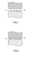
- Figures 1 and 2 are schematic cross-sectional views of opposing terminals before and after crimping respectively.
- the conductive particles 31 and the solder particles 32 between terminals before crimping by forming the anisotropic conductive adhesive into a structure which will be described below.
- the conductive particles 31, each of which is made from a resin particle as a core undergo a flattening deformation to produce elastic rebound against the deformation, thus keeping electrical connection.
- the solder particles 32 are also crushed and, due to solder bonding caused by heating, form a metallic bond which increases contact area with terminals thus improving heat dissipation and electrical properties. Furthermore, the conductive particles, which have a resin core, mitigate stress generated by a difference in thermal expansion between a device and a substrate which prevents cracks in solder bonded parts and thus connection reliability can be improved.
- the conductive particle may be a resin particle manufactured from an epoxy resin, a phenol resin, an acrylic resin, an acrylonitrile-styrene (AS) resin, a benzoguanamine resin, a divinylbenzene based resin, or a styrene based resin among other resins and is covered with a metallic layer of Au, Ni, and/or Zn to form a metal-coated conductive particle. Because this metal-coated particle is easily crushable and deformable upon crimping, a large contact area to a wiring pattern is possible and unevenness in height of the wiring pattern can be accommodated.
- AS acrylonitrile-styrene
- the conductive particles are preferably included at 1 to 30% by volume relative to the binder. Additionally, the average diameter of the conductive particles (D50) is preferably 1 to 10 ⁇ m and more preferably 2 to 6 ⁇ m.
- Solder particles are, for example, as defined in JISZ 3282-1999, Sn-Pb based, Pb-Sn-Sb based, Sn-Sb based, Sn-Pb-Bi based, Bi-Sn based, Sn-Cu based, Sn-Pb-Cu based, Sn-In based, Sn-Ag based, Sn-Pb-Ag based, or Pb-Ag based, among others, and may be chosen according to connection conditions, terminal material, and other considerations. Additionally, the form of the solder particles can be chosen from among a granular form, a scaly form, or other forms. It should be noted that, to improve anisotropic properties, the solder particles may be covered with an electrically insulating layer.
- the preferable blending amount of the solder particles is 1 to 30% by volume. An insufficient volume of the solder particles adversely affects heat dissipation properties and an excessive volume of the solder particles adversely affects anisotropic properties and connection reliability.
- the average diameter (D50) of the solder particles is preferably 25 to 400% of the average diameter of the conductive particles. If the solder particles are too small in comparison with the conductive particles, the solder particles will not be held in place by the opposing terminal during crimping which leads to satisfactory solder bonding not taking place thus making excellent heat dissipation properties unobtainable. On the contrary, if the solder particles are too large in comparison with the conductive particles, anisotropic properties are lost and reliable connection properties are unobtainable.
- adhesive compositions used in conventional anisotropic conductive adhesives and anisotropic conductive films are curable epoxy adhesive agents containing alicyclic epoxy compounds, heterocyclic epoxy compounds, and hydrogenated epoxy compounds, among others as primary ingredients thereof.
- An example of a preferable heterocyclic epoxy compound is a compound intramolecularly having 2 or more epoxy groups.
- the aforementioned compounds may be in liquid or solid state.
- examples include glycidyl hexahydro bisphenol A, and 3,4-epoxycyclohexenyl methyl-3',-4'-epoxycyclohexene carboxylate, among others.
- 3,4-epoxycyclohexylmethyl 3',4'-epoxycyclohexanecarboxylate may preferably be used because this has an excellent rapid curing property and ensures optical transparency appropriate for mounting an LED device after curing.
- heterocyclic-based compounds include a triazine-ring containing epoxy compound and an especially preferable example is 1,3,5-tris(2,3-epoxypropyl)-1,3,5-triazine-2,4,6-(1H,3H,5H)-trione.
- hydrogenated epoxy compound hydrogenated compounds of the aforementioned alicyclic epoxy compounds, hetero-ring-based epoxy compounds, and other known hydrogenated epoxy resins may be used.
- Alicyclic epoxy compounds, hetero-ring-based epoxy compounds, and hydrogenated epoxy compounds may be used individually or in a combination of two or more. Furthermore, in addition to the aforementioned epoxy compounds and to the extent that the effects of this invention are not adversely affected, other epoxy compounds may be used.
- Examples of other epoxy compounds include glycidyl ethers obtained by reacting epichlorohydrin with polyhydric phenols including bisphenol A, bisphenol F, bisphenol S, tetramethyl bisphenol A, diallyl bisphenol A, hydroquinone, catechol, resorcinol, cresol, tetrabromobisphenol A, trihydroxybiphenyl, benzophenone, bisresorcinol, bisphenol hexafluoroacetone, tetramethyl bisphenol A, tetramethyl bisphenol F, tris(hydroxyphenyl)methane, bixylenol, phenolic novolac, cresol novolac; polyglycidyl ethers obtained by reacting epichlorohydrin with polyhydric aliphatic alcohols including glycerin, neopentyl glycol, ethylene glycol, propylene glycol, hexylene glycol, polyethylene glycol, polypropylene glycol; glycid
- curing agents examples include acid anhydrides, imidazole compounds, and dicyan, among others.
- preferable examples include methylhexahydrophthalic anhydride, among others.
- an adhesive composition in the cases of using an alicyclic epoxy compound and an alicyclic acid anhydride based curing agent, in respect to amounts of each to be used, because insufficient amounts of the alicyclic acid anhydride based curing agent leads to excessive uncured epoxy compound and excessive amounts of the alicyclic acid anhydride based curing agent tends to promote corrosion of adherends as an effect of remaining curing agent, with respect to 100 parts by mass of the alicyclic epoxy compound, 80 to 120 parts by mass of the alicyclic acid anhydride based curing agent is preferably used and 95 to 105 parts by mass of it is more preferably used.
- Such an anisotropic conductive adhesive ensures an excellent heat dissipation property and high connection reliability because conductive particles thereof undergo a flattening deformation during crimping due to pressure and solder particles thereof are crushed and form a metallic bond due to solder bonding caused by heat.
- anisotropic conductive adhesive by uniformly mixing an adhesive composition, conductive particles, and solder particles.
- a connective structure made using the aforementioned anisotropic conductive adhesive comprises conductive particles, each being a resin particle having a conductive metallic layer formed on the surface thereof, electrically connecting a terminal of a first electronic component and a terminal of a second electronic component, the terminal of the first electronic component and the terminal of the second electronic component are solder bonded, and solder particles having an average diameter smaller than that of the conductive particles are trapped between the terminal of the first electronic component and the terminal of the second electronic component.
- Preferable electronic components in this embodiment include driver ICs(Integrated Circuit) and LEDs (Light Emitting Diode), among other chips (devices).
- Figure 3 is a cross-sectional view illustrating an example configuration of an LED package.
- the LED package is connected to a substrate by using the anisotropic conductive adhesive comprising an adhesive agent material in which the conductive particles and the solder particles are dispersed.
- the LED device comprises a device substrate 11 made of sapphire and several layers formed thereon including, for example, a first conductive cladding layer 12 made of n-GaN, an active layer 13 made of In x Al y Ga 1-x-y N, and a second conductive cladding layer 14 made of p-GaN , thus forming a so-called double heterostructure. Additionally, a first conductive electrode 12a is formed on a part of the first conductive cladding layer 12 and a second conductive electrode 14a is formed on a part of the second conductive cladding layer 14. If voltage is applied across the first conductive electrode 12a and the second conductive electrode 14a of the LED device, carriers are concentrated in the active layer 13 and light is generated due to recoupling.
- the substrate includes a substrate material 21, a first conductive circuit pattern 22 and a second conductive circuit pattern 23 formed on the substrate material 21, and electrodes 22a and 23a formed at positions corresponding to the first and second conductive electrodes 12a and 14a of an LED device respectively.
- the anisotropic conductive adhesive includes, as previously mentioned, the conductive particles 31 and the solder particles 32 dispersed in the binder 33.
- terminals of the LED device (conductive electrodes 12a, 14a) and terminals of the substrate (conductive electrodes 22a, 23a) are electrically connected via the conductive particles, and the terminals of the LED device and terminals of the substrate are bonded by solder bonding.
- the solder particles 32 can reflect light from the active layer 13 to achieve a high luminance.
- terminals of the LED device in a flip-chip-mounting LED are designed to be large, with the passivation layer 15, larger amounts of the conductive particles and the solder particles can be trapped in the interval between the terminals of the LED device (electrodes 12a, 14a) and the terminals of the substrate (circuit patterns 22, 23).
- heat generated at the active layer 13 of the LED device can be dissipated to the substrate more efficiently.
- the package manufacturing method according to this embodiment is a package manufacturing method wherein the conductive particles and the solder particles, which have a smaller average diameter in comparison to the conductive particles, are dispersed in an adhesive agent material to make an anisotropic conductive adhesive which is held between the terminal of the first electronic component and the terminal of a second electronic component, and the first electronic component and the second electronic component are thermally compressed.
- the terminal of the first electronic component and the terminal of the second electronic component are electrically connected via the conductive particles to form a connective structure wherein the first electronic component and the terminal of the second electronic component are solder bonded.
- the conductive particles undergo a flattening deformation due to pressure, the solder particles are crushed at the same time and form a metallic bond due to heat induced solder bonding thereby increasing opposing terminal contact surface area thus enabling high heat dissipation and high reliability properties. Additionally, as resin cores of the conductive particles mitigate stress generated by different amounts of thermal expansion in a substrate and a device, cracks in solder bonded parts can be suppressed.
- an anisotropic conductive adhesive in the form of an anisotropic conductive paste (ACP) and an LED package were manufactured, and heat dissipation properties, adhesive properties, and electrical properties thereof were evaluated.
- Conductive particles (product name: AUL705 manufactured by Sekisui Chemical Co., Ltd.) comprised of cross-linked polystyrene particles having an average diameter (D50) of 5 ⁇ m and having a gold coating applied to the surface thereof, and solder particles (product name: M707, manufactured by Senju Metal Industry Co., Ltd.) having an average diameter of 5 ⁇ m were dispersed in a mixture of a curable epoxy adhesive agent (epoxy resin (product name: CEL2021P, manufactured by Daicel Corporation) and acid anhydride (MeHHPA, product name: MH700, manufactured by New Japan Chemical Co., Ltd.) to manufacture an anisotropic conductive adhesive having a heat conductive property.
- a curable epoxy adhesive agent epoxy resin (product name: CEL2021P, manufactured by Daicel Corporation) and acid anhydride (MeHHPA, product name: MH700, manufactured by New Japan Chemical Co., Ltd.
- the anisotropic conductive adhesive was applied to an Au substrate terminal, the LED package was aligned, installed and thermal compression was performed with conditions of a load of 1000 g per chip and a temperature of 150°C for 10 seconds followed by a temperature of 230°C for 30 seconds.
- thermal resistance (°C/W) of the LED package was measured. Measurements were performed with a forward current (If) of 350mA (constant current control).
- a mixture of the conductive particles at 8% by volume and the solder particles at 2% by volume were dispersed in the epoxy composition to manufacture an anisotropic conductive adhesive with a heat conductive property.
- Results of measuring an LED package manufactured using this anisotropic conductive adhesive were a thermal resistance of 21.0 °C /W and a die shear strength of 26 N/chip. Additionally, electrical properties evaluation results in the high temperature and high humidity tests were P for the initial and P for the final measurements and electrical properties evaluation results in the thermal shock test were P for the initial and P for the final measurements.
- a mixture of the conductive particles at 5% by volume and the solder particles at 5% by volume were blended in an epoxy composition to manufacture an anisotropic conductive adhesive with a heat conductive property.
- Results of measuring an LED package manufactured using this anisotropic conductive adhesive were a thermal resistance of 13.2 °C /W and a die shear strength of 37 N/chip. Additionally, electrical properties evaluation results in the high temperature and high humidity tests were P for the initial and P for the final measurements and electrical properties evaluation results in the thermal shock test were P for the initial and P for the final measurements.
- a mixture of the conductive particles at 2% by volume and the solder particles at 8% by volume were blended in an epoxy composition to manufacture an anisotropic conductive adhesive with a heat conductive property.
- Results of measuring an LED package manufactured using this anisotropic conductive adhesive were a thermal resistance of 12.2 °C /W and a die shear strength of 45 N/chip. Additionally, electrical properties evaluation results in the high temperature and high humidity tests were P for the initial and P for the final measurements and electrical properties evaluation results in the thermal shock test were P for the initial and P for the final measurements.
- a mixture of the conductive particles at 2% by volume and the solder particles at 20% by volume were blended in an epoxy composition to manufacture an anisotropic conductive adhesive with a heat conductive property.
- Results of measuring an LED package manufactured using this anisotropic conductive adhesive were a thermal resistance of 10.4 °C /W and a die shear strength of 52 N/chip. Additionally, electrical properties evaluation results in the high temperature and high humidity tests were P for the initial and P for the final measurements and electrical properties evaluation results in the thermal shock test were P for the initial and P for the final measurements.
- a mixture of the conductive particles at 1% by volume, the solder particles at 30% by volume were blended in an epoxy composition to manufacture an anisotropic conductive adhesive with a heat conductive property.
- Results of measuring an LED package manufactured using this anisotropic conductive adhesive were a thermal resistance of 10.0 °C /W and a die shear strength of 54 N/chip. Additionally, electrical properties evaluation results in the high temperature and high humidity tests were P for the initial and P for the final measurements and electrical properties evaluation results in the thermal shock test were P for the initial and P for the final measurements.
- a mixture of the conductive particles at 30% by volume and the solder particles at 1% by volume were blended in an epoxy composition to manufacture an anisotropic conductive adhesive with a heat conductive property.
- Results of measuring an LED package manufactured using this anisotropic conductive adhesive were a thermal resistance of 31.9 °C /W and a die shear strength of 21 N/chip. Additionally, electrical properties evaluation results in the high temperature and high humidity tests were P for the initial and P for the final measurements and electrical properties evaluation results in the thermal shock test were P for the initial and P for the final measurements.
- thermal resistance is 21.0 (°C/W) and it is possible to achieve a thermal resistance value lower than that of the comparative example 2, to which solder particles were not added, and thus the heat dissipation properties in the LED package were improved.
- die shear strength was 26 N/chip which is an improvement in comparison with comparative example 2.
- RH relative humidity
- thermal resistance is 13.2 (°C/W) and it is possible to achieve a thermal resistance value lower than that of the comparative example 2, to which solder particles were not added, and thus the heat dissipation properties in the LED package were improved.
- die shear strength was 37 N/chip which is an improvement in comparison with comparative example 2.
- RH relative humidity
- thermal resistance is 12.2 (°C/W) and it is possible to achieve a thermal resistance value lower than that of the comparative example 2, to which solder particles were not added, and thus the heat dissipation properties in the LED package were improved.
- die shear strength was 45 N/chip which is an improvement in comparison with comparative example 2.
- RH relative humidity
- thermal resistance is 10.4 (°C/W) and it is possible to achieve a thermal resistance value lower than that the comparative example 2, to which the solder particles were not added, and thus the heat dissipation properties in the LED package were improved.
- die shear strength was 52 N/chip which is an improvement in comparison with comparative example 2.
- RH relative humidity
- thermal resistance is 10.0 (°C/W) and it is possible to achieve a thermal resistance value lower than that of the comparative example 2, to which solder particles were not added, and thus the heat dissipation properties in the LED package were improved.
- die shear strength was 54 N/chip which is an improvement in comparison with comparative example 2.
- RH relative humidity
- thermal resistance is 31.9 (°C/W) and it is possible to achieve a thermal resistance value lower than that of the comparative example 2, to which solder particles were not added, and thus the heat dissipation properties in the LED package were improved.
- die shear strength was 21 N/chip which is an improvement in comparison with comparative example 2.
- RH relative humidity
- thermal resistance is 11.8 (°C/W) and it is possible to achieve a thermal resistance value lower than that of the comparative example 2, to which solder particles were not added, and thus the heat dissipation properties in the LED package were improved.
- die shear strength was 48 N/chip which is an improvement in comparison with comparative example 2.
- RH relative humidity
- solder particles and conductive particles together in an anisotropic conductive adhesive it is possible to impart a high heat dissipation property to an LED package and obtain an anisotropic conductive adhesive with a high connection reliability.
Landscapes
- Engineering & Computer Science (AREA)
- Mechanical Engineering (AREA)
- Chemical & Material Sciences (AREA)
- Organic Chemistry (AREA)
- Spectroscopy & Molecular Physics (AREA)
- Dispersion Chemistry (AREA)
- Physics & Mathematics (AREA)
- Manufacturing & Machinery (AREA)
- Microelectronics & Electronic Packaging (AREA)
- Wire Bonding (AREA)
- Adhesives Or Adhesive Processes (AREA)
- Led Device Packages (AREA)
- Conductive Materials (AREA)
- Electric Connection Of Electric Components To Printed Circuits (AREA)
- Non-Insulated Conductors (AREA)
Applications Claiming Priority (2)
| Application Number | Priority Date | Filing Date | Title |
|---|---|---|---|
| JP2012210224A JP2014065766A (ja) | 2012-09-24 | 2012-09-24 | 異方性導電接着剤 |
| PCT/JP2013/075048 WO2014046093A1 (ja) | 2012-09-24 | 2013-09-17 | 異方性導電接着剤 |
Publications (3)
| Publication Number | Publication Date |
|---|---|
| EP2899245A1 true EP2899245A1 (de) | 2015-07-29 |
| EP2899245A4 EP2899245A4 (de) | 2016-06-01 |
| EP2899245B1 EP2899245B1 (de) | 2017-11-08 |
Family
ID=50341403
Family Applications (1)
| Application Number | Title | Priority Date | Filing Date |
|---|---|---|---|
| EP13840056.9A Active EP2899245B1 (de) | 2012-09-24 | 2013-09-17 | Anisotropes und leitfähiges haftmittel |
Country Status (8)
| Country | Link |
|---|---|
| US (1) | US9676066B2 (de) |
| EP (1) | EP2899245B1 (de) |
| JP (1) | JP2014065766A (de) |
| KR (1) | KR102159992B1 (de) |
| CN (1) | CN104662118B (de) |
| HK (1) | HK1209450A1 (de) |
| TW (1) | TWI626293B (de) |
| WO (1) | WO2014046093A1 (de) |
Families Citing this family (32)
| Publication number | Priority date | Publication date | Assignee | Title |
|---|---|---|---|---|
| WO2015056754A1 (ja) * | 2013-10-17 | 2015-04-23 | デクセリアルズ株式会社 | 異方性導電接着剤及び接続構造体 |
| JP6450923B2 (ja) * | 2013-12-20 | 2019-01-16 | パナソニックIpマネジメント株式会社 | 電子部品実装システムおよび電子部品実装方法ならびに電子部品実装装置 |
| JP6432416B2 (ja) * | 2014-04-14 | 2018-12-05 | 日亜化学工業株式会社 | 半導体装置 |
| JP6419457B2 (ja) * | 2014-05-23 | 2018-11-07 | デクセリアルズ株式会社 | 接着剤及び接続構造体 |
| WO2015178482A1 (ja) | 2014-05-23 | 2015-11-26 | デクセリアルズ株式会社 | 接着剤及び接続構造体 |
| JP6430148B2 (ja) * | 2014-05-23 | 2018-11-28 | デクセリアルズ株式会社 | 接着剤及び接続構造体 |
| CN107006131A (zh) * | 2014-07-28 | 2017-08-01 | 通用汽车环球科技运作有限责任公司 | 用于增强的粘合剂结合的系统和方法 |
| KR102055114B1 (ko) * | 2015-06-02 | 2019-12-12 | 데쿠세리아루즈 가부시키가이샤 | 접착제 조성물 |
| JP6519407B2 (ja) * | 2015-08-26 | 2019-05-29 | 日亜化学工業株式会社 | 発光装置及び発光装置の製造方法 |
| JP6710120B2 (ja) * | 2015-09-30 | 2020-06-17 | 太陽インキ製造株式会社 | 導電性接着剤、電子部品および電子部品の製造方法 |
| CN105336275A (zh) * | 2015-10-28 | 2016-02-17 | 江苏新广联半导体有限公司 | 高密rgb倒装led显示屏封装结构及制造方法 |
| CN106132086A (zh) * | 2016-07-08 | 2016-11-16 | 广东小天才科技有限公司 | 一种电路板结构及电子元件焊接方法 |
| CN105921909A (zh) * | 2016-07-18 | 2016-09-07 | 浙江亚通焊材有限公司 | 一种用于制备高温粘带纤料的粘结剂及高温粘带纤料 |
| JP2018088498A (ja) * | 2016-11-29 | 2018-06-07 | デクセリアルズ株式会社 | 異方性導電接着剤 |
| KR102555383B1 (ko) * | 2016-12-07 | 2023-07-12 | 엘지디스플레이 주식회사 | 유기발광소자를 이용한 조명장치 및 그 제조방법 |
| TWI761477B (zh) * | 2017-03-30 | 2022-04-21 | 日商太陽油墨製造股份有限公司 | 導電性接著劑、硬化物、電子零件及電子零件之製造方法 |
| TWI736695B (zh) * | 2017-10-24 | 2021-08-21 | 啟耀光電股份有限公司 | 電子裝置與其製造方法 |
| CN109728022B (zh) * | 2017-10-31 | 2023-06-20 | 英属开曼群岛商錼创科技股份有限公司 | 微型发光二极管显示面板及其制造方法 |
| TWI650854B (zh) * | 2017-10-31 | 2019-02-11 | 英屬開曼群島商錼創科技股份有限公司 | 微型發光二極體顯示面板及其製造方法 |
| KR101985499B1 (ko) * | 2017-12-28 | 2019-06-03 | 삼화콘덴서공업 주식회사 | 과전류 보호 기능을 가지는 금속 산화물 바리스터 |
| JP7185252B2 (ja) | 2018-01-31 | 2022-12-07 | 三国電子有限会社 | 接続構造体の作製方法 |
| JP7046351B2 (ja) | 2018-01-31 | 2022-04-04 | 三国電子有限会社 | 接続構造体の作製方法 |
| JP7160302B2 (ja) * | 2018-01-31 | 2022-10-25 | 三国電子有限会社 | 接続構造体および接続構造体の作製方法 |
| KR102769519B1 (ko) | 2018-02-14 | 2025-02-17 | 에피스타 코포레이션 | 발광 장치, 그 제조 방법 및 디스플레이 모듈 |
| TW202349704A (zh) * | 2018-02-14 | 2023-12-16 | 晶元光電股份有限公司 | 發光裝置、其製造方法及顯示模組 |
| CN110880544B (zh) * | 2018-09-06 | 2021-09-03 | 深圳市斯迈得半导体有限公司 | 一种用于玻璃基板的芯片及其制作方法 |
| CN110635017B (zh) * | 2019-08-09 | 2021-07-09 | 惠州市志金电子科技有限公司 | 一种miniled背光基板封装方法 |
| TWI819073B (zh) * | 2019-08-22 | 2023-10-21 | 晶元光電股份有限公司 | 發光裝置、其製造方法及顯示模組 |
| KR102270303B1 (ko) * | 2019-08-23 | 2021-06-30 | 삼성전기주식회사 | 적층형 커패시터 및 그 실장 기판 |
| CN111048499B (zh) * | 2019-12-16 | 2022-05-13 | 业成科技(成都)有限公司 | 微发光二极管显示面板及其制备方法 |
| US11901497B2 (en) * | 2019-12-24 | 2024-02-13 | Seoul Viosys Co., Ltd. | Method of repairing light emitting device, apparatus for repairing light emitting device, and display panel having repaired light emitting device |
| CN116631294A (zh) * | 2023-05-22 | 2023-08-22 | 业成科技(成都)有限公司 | 透明显示面板及其拼接方法 |
Family Cites Families (21)
| Publication number | Priority date | Publication date | Assignee | Title |
|---|---|---|---|---|
| JPS60178690A (ja) | 1984-02-24 | 1985-09-12 | ソニ−ケミカル株式会社 | 配線基板 |
| JPH0773067B2 (ja) * | 1987-08-31 | 1995-08-02 | 日立化成工業株式会社 | 回路の接続部材 |
| US5001542A (en) * | 1988-12-05 | 1991-03-19 | Hitachi Chemical Company | Composition for circuit connection, method for connection using the same, and connected structure of semiconductor chips |
| JPH03129607A (ja) * | 1989-10-14 | 1991-06-03 | Sony Chem Corp | 異方性導電膜 |
| JPH04180029A (ja) * | 1990-11-15 | 1992-06-26 | Seiko Epson Corp | 回路の接続構造体 |
| JP2948038B2 (ja) * | 1992-12-18 | 1999-09-13 | 住友ベークライト株式会社 | 異方導電フィルム |
| JPH08102218A (ja) * | 1994-09-30 | 1996-04-16 | Nec Corp | 異方性導電フィルム |
| JP3417110B2 (ja) | 1994-12-30 | 2003-06-16 | カシオ計算機株式会社 | 電子部品の接続方法 |
| JPH114064A (ja) | 1997-06-12 | 1999-01-06 | Nec Corp | 異方性導電樹脂及びこれを用いた電子部品の実装構造 |
| US5965064A (en) * | 1997-10-28 | 1999-10-12 | Sony Chemicals Corporation | Anisotropically electroconductive adhesive and adhesive film |
| JPH11176879A (ja) | 1997-12-12 | 1999-07-02 | Citizen Watch Co Ltd | 半導体装置の実装方法およびこれに用いる異方性導電接着剤 |
| JP3002965B2 (ja) * | 1997-12-29 | 2000-01-24 | 株式会社三井ハイテック | 電子部品の面実装用接続部材 |
| JP3119230B2 (ja) * | 1998-03-03 | 2000-12-18 | 日本電気株式会社 | 樹脂フィルムおよびこれを用いた電子部品の接続方法 |
| JP2002299378A (ja) * | 2001-03-30 | 2002-10-11 | Lintec Corp | 導電体付接着シート、半導体装置製造方法および半導体装置 |
| JP2006108523A (ja) * | 2004-10-08 | 2006-04-20 | Hitachi Chem Co Ltd | 異方性導電フィルムを用いた電気部品の接続方法 |
| WO2006103918A1 (ja) * | 2005-03-28 | 2006-10-05 | Matsushita Electric Industrial Co., Ltd. | フリップチップ実装体とフリップチップ実装方法及びフリップチップ実装装置 |
| JP4432949B2 (ja) | 2006-09-15 | 2010-03-17 | パナソニック株式会社 | 電気部品の接続方法 |
| JP5499448B2 (ja) * | 2008-07-16 | 2014-05-21 | デクセリアルズ株式会社 | 異方性導電接着剤 |
| US10141084B2 (en) * | 2010-10-08 | 2018-11-27 | Cheil Industries, Inc. | Electronic device |
| JP5596767B2 (ja) * | 2011-11-02 | 2014-09-24 | 積水化学工業株式会社 | 異方性導電材料及び接続構造体 |
| JP2013118181A (ja) * | 2011-11-02 | 2013-06-13 | Sekisui Chem Co Ltd | 異方性導電材料及び接続構造体 |
-
2012
- 2012-09-24 JP JP2012210224A patent/JP2014065766A/ja active Pending
-
2013
- 2013-09-17 EP EP13840056.9A patent/EP2899245B1/de active Active
- 2013-09-17 HK HK15110096.5A patent/HK1209450A1/xx unknown
- 2013-09-17 KR KR1020157009198A patent/KR102159992B1/ko active Active
- 2013-09-17 CN CN201380049646.2A patent/CN104662118B/zh active Active
- 2013-09-17 TW TW102133614A patent/TWI626293B/zh active
- 2013-09-17 WO PCT/JP2013/075048 patent/WO2014046093A1/ja not_active Ceased
- 2013-09-17 US US14/423,887 patent/US9676066B2/en active Active
Also Published As
| Publication number | Publication date |
|---|---|
| CN104662118A (zh) | 2015-05-27 |
| KR102159992B1 (ko) | 2020-09-25 |
| CN104662118B (zh) | 2017-08-18 |
| TW201412933A (zh) | 2014-04-01 |
| EP2899245B1 (de) | 2017-11-08 |
| WO2014046093A1 (ja) | 2014-03-27 |
| US9676066B2 (en) | 2017-06-13 |
| HK1209450A1 (en) | 2016-04-01 |
| US20150209914A1 (en) | 2015-07-30 |
| KR20150060757A (ko) | 2015-06-03 |
| JP2014065766A (ja) | 2014-04-17 |
| TWI626293B (zh) | 2018-06-11 |
| EP2899245A4 (de) | 2016-06-01 |
Similar Documents
| Publication | Publication Date | Title |
|---|---|---|
| EP2899245B1 (de) | Anisotropes und leitfähiges haftmittel | |
| US9670385B2 (en) | Anisotropic conductive adhesive | |
| KR102096575B1 (ko) | 이방성 도전 접착제 및 접속 구조체 | |
| TWI574594B (zh) | A method of manufacturing a connecting structure and an anisotropic conductive adhesive | |
| JP2015088744A (ja) | 発光装置、異方性導電接着剤、発光装置製造方法 | |
| TW201533212A (zh) | 異向性導電接著劑及連接結構體 | |
| KR102368748B1 (ko) | 접착제 및 접속 구조체 | |
| TWI669721B (zh) | Anisotropic conductive adhesive | |
| TWI789406B (zh) | 導電性接著劑組成物及使用其的連接結構體、製造連接結構體的方法 | |
| JP2014065765A (ja) | 異方性導電接着剤 | |
| WO2021131586A1 (ja) | 異方性導電接着剤 |
Legal Events
| Date | Code | Title | Description |
|---|---|---|---|
| PUAI | Public reference made under article 153(3) epc to a published international application that has entered the european phase |
Free format text: ORIGINAL CODE: 0009012 |
|
| 17P | Request for examination filed |
Effective date: 20150205 |
|
| AK | Designated contracting states |
Kind code of ref document: A1 Designated state(s): AL AT BE BG CH CY CZ DE DK EE ES FI FR GB GR HR HU IE IS IT LI LT LU LV MC MK MT NL NO PL PT RO RS SE SI SK SM TR |
|
| AX | Request for extension of the european patent |
Extension state: BA ME |
|
| DAX | Request for extension of the european patent (deleted) | ||
| RA4 | Supplementary search report drawn up and despatched (corrected) |
Effective date: 20160503 |
|
| RIC1 | Information provided on ipc code assigned before grant |
Ipc: H01B 1/22 20060101ALI20160427BHEP Ipc: C09J 9/02 20060101ALI20160427BHEP Ipc: C09J 11/02 20060101ALI20160427BHEP Ipc: H01B 1/00 20060101ALI20160427BHEP Ipc: C09J 201/00 20060101AFI20160427BHEP Ipc: H01B 5/16 20060101ALI20160427BHEP Ipc: H01L 21/60 20060101ALI20160427BHEP |
|
| GRAP | Despatch of communication of intention to grant a patent |
Free format text: ORIGINAL CODE: EPIDOSNIGR1 |
|
| INTG | Intention to grant announced |
Effective date: 20170119 |
|
| GRAJ | Information related to disapproval of communication of intention to grant by the applicant or resumption of examination proceedings by the epo deleted |
Free format text: ORIGINAL CODE: EPIDOSDIGR1 |
|
| INTC | Intention to grant announced (deleted) | ||
| GRAP | Despatch of communication of intention to grant a patent |
Free format text: ORIGINAL CODE: EPIDOSNIGR1 |
|
| INTG | Intention to grant announced |
Effective date: 20170524 |
|
| GRAS | Grant fee paid |
Free format text: ORIGINAL CODE: EPIDOSNIGR3 |
|
| GRAA | (expected) grant |
Free format text: ORIGINAL CODE: 0009210 |
|
| AK | Designated contracting states |
Kind code of ref document: B1 Designated state(s): AL AT BE BG CH CY CZ DE DK EE ES FI FR GB GR HR HU IE IS IT LI LT LU LV MC MK MT NL NO PL PT RO RS SE SI SK SM TR |
|
| REG | Reference to a national code |
Ref country code: GB Ref legal event code: FG4D |
|
| REG | Reference to a national code |
Ref country code: CH Ref legal event code: EP Ref country code: AT Ref legal event code: REF Ref document number: 944126 Country of ref document: AT Kind code of ref document: T Effective date: 20171115 |
|
| REG | Reference to a national code |
Ref country code: IE Ref legal event code: FG4D |
|
| REG | Reference to a national code |
Ref country code: DE Ref legal event code: R096 Ref document number: 602013029267 Country of ref document: DE |
|
| REG | Reference to a national code |
Ref country code: NL Ref legal event code: MP Effective date: 20171108 |
|
| REG | Reference to a national code |
Ref country code: LT Ref legal event code: MG4D |
|
| REG | Reference to a national code |
Ref country code: AT Ref legal event code: MK05 Ref document number: 944126 Country of ref document: AT Kind code of ref document: T Effective date: 20171108 |
|
| PG25 | Lapsed in a contracting state [announced via postgrant information from national office to epo] |
Ref country code: ES Free format text: LAPSE BECAUSE OF FAILURE TO SUBMIT A TRANSLATION OF THE DESCRIPTION OR TO PAY THE FEE WITHIN THE PRESCRIBED TIME-LIMIT Effective date: 20171108 Ref country code: NO Free format text: LAPSE BECAUSE OF FAILURE TO SUBMIT A TRANSLATION OF THE DESCRIPTION OR TO PAY THE FEE WITHIN THE PRESCRIBED TIME-LIMIT Effective date: 20180208 Ref country code: NL Free format text: LAPSE BECAUSE OF FAILURE TO SUBMIT A TRANSLATION OF THE DESCRIPTION OR TO PAY THE FEE WITHIN THE PRESCRIBED TIME-LIMIT Effective date: 20171108 Ref country code: SE Free format text: LAPSE BECAUSE OF FAILURE TO SUBMIT A TRANSLATION OF THE DESCRIPTION OR TO PAY THE FEE WITHIN THE PRESCRIBED TIME-LIMIT Effective date: 20171108 Ref country code: LT Free format text: LAPSE BECAUSE OF FAILURE TO SUBMIT A TRANSLATION OF THE DESCRIPTION OR TO PAY THE FEE WITHIN THE PRESCRIBED TIME-LIMIT Effective date: 20171108 Ref country code: FI Free format text: LAPSE BECAUSE OF FAILURE TO SUBMIT A TRANSLATION OF THE DESCRIPTION OR TO PAY THE FEE WITHIN THE PRESCRIBED TIME-LIMIT Effective date: 20171108 |
|
| PG25 | Lapsed in a contracting state [announced via postgrant information from national office to epo] |
Ref country code: BG Free format text: LAPSE BECAUSE OF FAILURE TO SUBMIT A TRANSLATION OF THE DESCRIPTION OR TO PAY THE FEE WITHIN THE PRESCRIBED TIME-LIMIT Effective date: 20180208 Ref country code: HR Free format text: LAPSE BECAUSE OF FAILURE TO SUBMIT A TRANSLATION OF THE DESCRIPTION OR TO PAY THE FEE WITHIN THE PRESCRIBED TIME-LIMIT Effective date: 20171108 Ref country code: GR Free format text: LAPSE BECAUSE OF FAILURE TO SUBMIT A TRANSLATION OF THE DESCRIPTION OR TO PAY THE FEE WITHIN THE PRESCRIBED TIME-LIMIT Effective date: 20180209 Ref country code: IS Free format text: LAPSE BECAUSE OF FAILURE TO SUBMIT A TRANSLATION OF THE DESCRIPTION OR TO PAY THE FEE WITHIN THE PRESCRIBED TIME-LIMIT Effective date: 20180308 Ref country code: RS Free format text: LAPSE BECAUSE OF FAILURE TO SUBMIT A TRANSLATION OF THE DESCRIPTION OR TO PAY THE FEE WITHIN THE PRESCRIBED TIME-LIMIT Effective date: 20171108 Ref country code: LV Free format text: LAPSE BECAUSE OF FAILURE TO SUBMIT A TRANSLATION OF THE DESCRIPTION OR TO PAY THE FEE WITHIN THE PRESCRIBED TIME-LIMIT Effective date: 20171108 Ref country code: AT Free format text: LAPSE BECAUSE OF FAILURE TO SUBMIT A TRANSLATION OF THE DESCRIPTION OR TO PAY THE FEE WITHIN THE PRESCRIBED TIME-LIMIT Effective date: 20171108 |
|
| PG25 | Lapsed in a contracting state [announced via postgrant information from national office to epo] |
Ref country code: DK Free format text: LAPSE BECAUSE OF FAILURE TO SUBMIT A TRANSLATION OF THE DESCRIPTION OR TO PAY THE FEE WITHIN THE PRESCRIBED TIME-LIMIT Effective date: 20171108 Ref country code: CY Free format text: LAPSE BECAUSE OF FAILURE TO SUBMIT A TRANSLATION OF THE DESCRIPTION OR TO PAY THE FEE WITHIN THE PRESCRIBED TIME-LIMIT Effective date: 20171108 Ref country code: EE Free format text: LAPSE BECAUSE OF FAILURE TO SUBMIT A TRANSLATION OF THE DESCRIPTION OR TO PAY THE FEE WITHIN THE PRESCRIBED TIME-LIMIT Effective date: 20171108 Ref country code: CZ Free format text: LAPSE BECAUSE OF FAILURE TO SUBMIT A TRANSLATION OF THE DESCRIPTION OR TO PAY THE FEE WITHIN THE PRESCRIBED TIME-LIMIT Effective date: 20171108 Ref country code: SK Free format text: LAPSE BECAUSE OF FAILURE TO SUBMIT A TRANSLATION OF THE DESCRIPTION OR TO PAY THE FEE WITHIN THE PRESCRIBED TIME-LIMIT Effective date: 20171108 |
|
| REG | Reference to a national code |
Ref country code: DE Ref legal event code: R097 Ref document number: 602013029267 Country of ref document: DE |
|
| PG25 | Lapsed in a contracting state [announced via postgrant information from national office to epo] |
Ref country code: PL Free format text: LAPSE BECAUSE OF FAILURE TO SUBMIT A TRANSLATION OF THE DESCRIPTION OR TO PAY THE FEE WITHIN THE PRESCRIBED TIME-LIMIT Effective date: 20171108 Ref country code: RO Free format text: LAPSE BECAUSE OF FAILURE TO SUBMIT A TRANSLATION OF THE DESCRIPTION OR TO PAY THE FEE WITHIN THE PRESCRIBED TIME-LIMIT Effective date: 20171108 Ref country code: IT Free format text: LAPSE BECAUSE OF FAILURE TO SUBMIT A TRANSLATION OF THE DESCRIPTION OR TO PAY THE FEE WITHIN THE PRESCRIBED TIME-LIMIT Effective date: 20171108 Ref country code: SM Free format text: LAPSE BECAUSE OF FAILURE TO SUBMIT A TRANSLATION OF THE DESCRIPTION OR TO PAY THE FEE WITHIN THE PRESCRIBED TIME-LIMIT Effective date: 20171108 |
|
| PLBE | No opposition filed within time limit |
Free format text: ORIGINAL CODE: 0009261 |
|
| STAA | Information on the status of an ep patent application or granted ep patent |
Free format text: STATUS: NO OPPOSITION FILED WITHIN TIME LIMIT |
|
| 26N | No opposition filed |
Effective date: 20180809 |
|
| PG25 | Lapsed in a contracting state [announced via postgrant information from national office to epo] |
Ref country code: SI Free format text: LAPSE BECAUSE OF FAILURE TO SUBMIT A TRANSLATION OF THE DESCRIPTION OR TO PAY THE FEE WITHIN THE PRESCRIBED TIME-LIMIT Effective date: 20171108 |
|
| PG25 | Lapsed in a contracting state [announced via postgrant information from national office to epo] |
Ref country code: MC Free format text: LAPSE BECAUSE OF FAILURE TO SUBMIT A TRANSLATION OF THE DESCRIPTION OR TO PAY THE FEE WITHIN THE PRESCRIBED TIME-LIMIT Effective date: 20171108 |
|
| REG | Reference to a national code |
Ref country code: CH Ref legal event code: PL |
|
| GBPC | Gb: european patent ceased through non-payment of renewal fee |
Effective date: 20180917 |
|
| REG | Reference to a national code |
Ref country code: BE Ref legal event code: MM Effective date: 20180930 |
|
| REG | Reference to a national code |
Ref country code: IE Ref legal event code: MM4A |
|
| PG25 | Lapsed in a contracting state [announced via postgrant information from national office to epo] |
Ref country code: LU Free format text: LAPSE BECAUSE OF NON-PAYMENT OF DUE FEES Effective date: 20180917 |
|
| PG25 | Lapsed in a contracting state [announced via postgrant information from national office to epo] |
Ref country code: IE Free format text: LAPSE BECAUSE OF NON-PAYMENT OF DUE FEES Effective date: 20180917 |
|
| PG25 | Lapsed in a contracting state [announced via postgrant information from national office to epo] |
Ref country code: FR Free format text: LAPSE BECAUSE OF NON-PAYMENT OF DUE FEES Effective date: 20180930 Ref country code: CH Free format text: LAPSE BECAUSE OF NON-PAYMENT OF DUE FEES Effective date: 20180930 Ref country code: LI Free format text: LAPSE BECAUSE OF NON-PAYMENT OF DUE FEES Effective date: 20180930 Ref country code: BE Free format text: LAPSE BECAUSE OF NON-PAYMENT OF DUE FEES Effective date: 20180930 |
|
| PG25 | Lapsed in a contracting state [announced via postgrant information from national office to epo] |
Ref country code: GB Free format text: LAPSE BECAUSE OF NON-PAYMENT OF DUE FEES Effective date: 20180917 |
|
| PG25 | Lapsed in a contracting state [announced via postgrant information from national office to epo] |
Ref country code: MT Free format text: LAPSE BECAUSE OF NON-PAYMENT OF DUE FEES Effective date: 20180917 |
|
| PG25 | Lapsed in a contracting state [announced via postgrant information from national office to epo] |
Ref country code: TR Free format text: LAPSE BECAUSE OF FAILURE TO SUBMIT A TRANSLATION OF THE DESCRIPTION OR TO PAY THE FEE WITHIN THE PRESCRIBED TIME-LIMIT Effective date: 20171108 |
|
| PG25 | Lapsed in a contracting state [announced via postgrant information from national office to epo] |
Ref country code: PT Free format text: LAPSE BECAUSE OF FAILURE TO SUBMIT A TRANSLATION OF THE DESCRIPTION OR TO PAY THE FEE WITHIN THE PRESCRIBED TIME-LIMIT Effective date: 20171108 |
|
| PG25 | Lapsed in a contracting state [announced via postgrant information from national office to epo] |
Ref country code: HU Free format text: LAPSE BECAUSE OF FAILURE TO SUBMIT A TRANSLATION OF THE DESCRIPTION OR TO PAY THE FEE WITHIN THE PRESCRIBED TIME-LIMIT; INVALID AB INITIO Effective date: 20130917 Ref country code: MK Free format text: LAPSE BECAUSE OF NON-PAYMENT OF DUE FEES Effective date: 20171108 |
|
| PG25 | Lapsed in a contracting state [announced via postgrant information from national office to epo] |
Ref country code: AL Free format text: LAPSE BECAUSE OF FAILURE TO SUBMIT A TRANSLATION OF THE DESCRIPTION OR TO PAY THE FEE WITHIN THE PRESCRIBED TIME-LIMIT Effective date: 20171108 |
|
| PGFP | Annual fee paid to national office [announced via postgrant information from national office to epo] |
Ref country code: DE Payment date: 20250730 Year of fee payment: 13 |