EP2940699B1 - Fil supraconducteur en oxyde - Google Patents
Fil supraconducteur en oxyde Download PDFInfo
- Publication number
- EP2940699B1 EP2940699B1 EP13868560.7A EP13868560A EP2940699B1 EP 2940699 B1 EP2940699 B1 EP 2940699B1 EP 13868560 A EP13868560 A EP 13868560A EP 2940699 B1 EP2940699 B1 EP 2940699B1
- Authority
- EP
- European Patent Office
- Prior art keywords
- layer
- oxide superconductor
- wire
- metal tape
- thickness
- Prior art date
- Legal status (The legal status is an assumption and is not a legal conclusion. Google has not performed a legal analysis and makes no representation as to the accuracy of the status listed.)
- Not-in-force
Links
- 239000002887 superconductor Substances 0.000 title claims description 271
- 239000010410 layer Substances 0.000 claims description 292
- 229910052751 metal Inorganic materials 0.000 claims description 97
- 239000002184 metal Substances 0.000 claims description 97
- 230000006641 stabilisation Effects 0.000 claims description 56
- 238000011105 stabilization Methods 0.000 claims description 56
- 229910000679 solder Inorganic materials 0.000 claims description 53
- 239000000758 substrate Substances 0.000 claims description 43
- 238000002844 melting Methods 0.000 claims description 20
- 230000008018 melting Effects 0.000 claims description 20
- 239000011229 interlayer Substances 0.000 claims description 18
- 229910001316 Ag alloy Inorganic materials 0.000 claims description 9
- 239000000463 material Substances 0.000 description 30
- 229910052760 oxygen Inorganic materials 0.000 description 16
- 230000000670 limiting effect Effects 0.000 description 15
- 238000000034 method Methods 0.000 description 15
- IJGRMHOSHXDMSA-UHFFFAOYSA-N Atomic nitrogen Chemical compound N#N IJGRMHOSHXDMSA-UHFFFAOYSA-N 0.000 description 14
- 230000000052 comparative effect Effects 0.000 description 11
- 239000010949 copper Substances 0.000 description 11
- 229910045601 alloy Inorganic materials 0.000 description 9
- 239000000956 alloy Substances 0.000 description 9
- QVGXLLKOCUKJST-UHFFFAOYSA-N atomic oxygen Chemical compound [O] QVGXLLKOCUKJST-UHFFFAOYSA-N 0.000 description 9
- 239000001301 oxygen Substances 0.000 description 9
- 238000009792 diffusion process Methods 0.000 description 8
- 229910052757 nitrogen Inorganic materials 0.000 description 8
- 239000007788 liquid Substances 0.000 description 7
- 230000002265 prevention Effects 0.000 description 7
- 239000000470 constituent Substances 0.000 description 6
- 239000013078 crystal Substances 0.000 description 6
- 229910000570 Cupronickel Inorganic materials 0.000 description 5
- CETPSERCERDGAM-UHFFFAOYSA-N ceric oxide Chemical compound O=[Ce]=O CETPSERCERDGAM-UHFFFAOYSA-N 0.000 description 5
- 229910000422 cerium(IV) oxide Inorganic materials 0.000 description 5
- 239000004020 conductor Substances 0.000 description 5
- 230000006866 deterioration Effects 0.000 description 5
- 230000000694 effects Effects 0.000 description 5
- 229910000856 hastalloy Inorganic materials 0.000 description 5
- 238000004519 manufacturing process Methods 0.000 description 5
- 229910044991 metal oxide Inorganic materials 0.000 description 5
- 150000004706 metal oxides Chemical group 0.000 description 5
- RYGMFSIKBFXOCR-UHFFFAOYSA-N Copper Chemical compound [Cu] RYGMFSIKBFXOCR-UHFFFAOYSA-N 0.000 description 4
- QPLDLSVMHZLSFG-UHFFFAOYSA-N Copper oxide Chemical compound [Cu]=O QPLDLSVMHZLSFG-UHFFFAOYSA-N 0.000 description 4
- 239000005751 Copper oxide Substances 0.000 description 4
- 229910052802 copper Inorganic materials 0.000 description 4
- 229910000431 copper oxide Inorganic materials 0.000 description 4
- UREBDLICKHMUKA-CXSFZGCWSA-N dexamethasone Chemical compound C1CC2=CC(=O)C=C[C@]2(C)[C@]2(F)[C@@H]1[C@@H]1C[C@@H](C)[C@@](C(=O)CO)(O)[C@@]1(C)C[C@@H]2O UREBDLICKHMUKA-CXSFZGCWSA-N 0.000 description 4
- 239000011888 foil Substances 0.000 description 4
- 238000010438 heat treatment Methods 0.000 description 4
- 238000007735 ion beam assisted deposition Methods 0.000 description 4
- 239000000203 mixture Substances 0.000 description 4
- RUDFQVOCFDJEEF-UHFFFAOYSA-N yttrium(III) oxide Inorganic materials [O-2].[O-2].[O-2].[Y+3].[Y+3] RUDFQVOCFDJEEF-UHFFFAOYSA-N 0.000 description 4
- 229910001369 Brass Inorganic materials 0.000 description 3
- 229910002609 Gd2Zr2O7 Inorganic materials 0.000 description 3
- 239000012790 adhesive layer Substances 0.000 description 3
- PNEYBMLMFCGWSK-UHFFFAOYSA-N aluminium oxide Inorganic materials [O-2].[O-2].[O-2].[Al+3].[Al+3] PNEYBMLMFCGWSK-UHFFFAOYSA-N 0.000 description 3
- 239000010951 brass Substances 0.000 description 3
- 238000006243 chemical reaction Methods 0.000 description 3
- YOCUPQPZWBBYIX-UHFFFAOYSA-N copper nickel Chemical compound [Ni].[Cu] YOCUPQPZWBBYIX-UHFFFAOYSA-N 0.000 description 3
- 229910052593 corundum Inorganic materials 0.000 description 3
- 230000001747 exhibiting effect Effects 0.000 description 3
- 239000007769 metal material Substances 0.000 description 3
- MOFOBJHOKRNACT-UHFFFAOYSA-N nickel silver Chemical compound [Ni].[Ag] MOFOBJHOKRNACT-UHFFFAOYSA-N 0.000 description 3
- 239000010956 nickel silver Substances 0.000 description 3
- 235000012771 pancakes Nutrition 0.000 description 3
- 230000002093 peripheral effect Effects 0.000 description 3
- 238000004544 sputter deposition Methods 0.000 description 3
- 230000007704 transition Effects 0.000 description 3
- 238000004804 winding Methods 0.000 description 3
- 229910001845 yogo sapphire Inorganic materials 0.000 description 3
- 229910000906 Bronze Inorganic materials 0.000 description 2
- 229910052688 Gadolinium Inorganic materials 0.000 description 2
- 102100022846 Histone acetyltransferase KAT2B Human genes 0.000 description 2
- 101001046967 Homo sapiens Histone acetyltransferase KAT2A Proteins 0.000 description 2
- 101001047006 Homo sapiens Histone acetyltransferase KAT2B Proteins 0.000 description 2
- XEEYBQQBJWHFJM-UHFFFAOYSA-N Iron Chemical compound [Fe] XEEYBQQBJWHFJM-UHFFFAOYSA-N 0.000 description 2
- 229910002328 LaMnO3 Inorganic materials 0.000 description 2
- 229910000990 Ni alloy Inorganic materials 0.000 description 2
- OAICVXFJPJFONN-UHFFFAOYSA-N Phosphorus Chemical compound [P] OAICVXFJPJFONN-UHFFFAOYSA-N 0.000 description 2
- MCMNRKCIXSYSNV-UHFFFAOYSA-N Zirconium dioxide Chemical compound O=[Zr]=O MCMNRKCIXSYSNV-UHFFFAOYSA-N 0.000 description 2
- 238000000137 annealing Methods 0.000 description 2
- 239000010974 bronze Substances 0.000 description 2
- KUNSUQLRTQLHQQ-UHFFFAOYSA-N copper tin Chemical compound [Cu].[Sn] KUNSUQLRTQLHQQ-UHFFFAOYSA-N 0.000 description 2
- JYTUFVYWTIKZGR-UHFFFAOYSA-N holmium oxide Inorganic materials [O][Ho]O[Ho][O] JYTUFVYWTIKZGR-UHFFFAOYSA-N 0.000 description 2
- 239000012535 impurity Substances 0.000 description 2
- 229910052761 rare earth metal Inorganic materials 0.000 description 2
- 239000002356 single layer Substances 0.000 description 2
- 230000001629 suppression Effects 0.000 description 2
- 229910052727 yttrium Inorganic materials 0.000 description 2
- 108010053481 Antifreeze Proteins Proteins 0.000 description 1
- 229910000952 Be alloy Inorganic materials 0.000 description 1
- 229910016338 Bi—Sn Inorganic materials 0.000 description 1
- VYZAMTAEIAYCRO-UHFFFAOYSA-N Chromium Chemical compound [Cr] VYZAMTAEIAYCRO-UHFFFAOYSA-N 0.000 description 1
- 229910017518 Cu Zn Inorganic materials 0.000 description 1
- 229910000881 Cu alloy Inorganic materials 0.000 description 1
- 229910017752 Cu-Zn Inorganic materials 0.000 description 1
- 229910017943 Cu—Zn Inorganic materials 0.000 description 1
- 229910052691 Erbium Inorganic materials 0.000 description 1
- ZOKXTWBITQBERF-UHFFFAOYSA-N Molybdenum Chemical compound [Mo] ZOKXTWBITQBERF-UHFFFAOYSA-N 0.000 description 1
- 229910052779 Neodymium Inorganic materials 0.000 description 1
- 229910052772 Samarium Inorganic materials 0.000 description 1
- 229910052581 Si3N4 Inorganic materials 0.000 description 1
- 229910020816 Sn Pb Inorganic materials 0.000 description 1
- 229910001128 Sn alloy Inorganic materials 0.000 description 1
- 229910020836 Sn-Ag Inorganic materials 0.000 description 1
- 229910020888 Sn-Cu Inorganic materials 0.000 description 1
- 229910020922 Sn-Pb Inorganic materials 0.000 description 1
- 229910020935 Sn-Sb Inorganic materials 0.000 description 1
- 229910020988 Sn—Ag Inorganic materials 0.000 description 1
- 229910019204 Sn—Cu Inorganic materials 0.000 description 1
- 229910008783 Sn—Pb Inorganic materials 0.000 description 1
- 229910008757 Sn—Sb Inorganic materials 0.000 description 1
- 229910001080 W alloy Inorganic materials 0.000 description 1
- 229910008253 Zr2O3 Inorganic materials 0.000 description 1
- 239000000853 adhesive Substances 0.000 description 1
- 230000001070 adhesive effect Effects 0.000 description 1
- 230000002411 adverse Effects 0.000 description 1
- 230000004888 barrier function Effects 0.000 description 1
- DMFGNRRURHSENX-UHFFFAOYSA-N beryllium copper Chemical compound [Be].[Cu] DMFGNRRURHSENX-UHFFFAOYSA-N 0.000 description 1
- 230000015572 biosynthetic process Effects 0.000 description 1
- 239000000919 ceramic Substances 0.000 description 1
- 229910052804 chromium Inorganic materials 0.000 description 1
- 239000011651 chromium Substances 0.000 description 1
- 229910017052 cobalt Inorganic materials 0.000 description 1
- 239000010941 cobalt Substances 0.000 description 1
- GUTLYIVDDKVIGB-UHFFFAOYSA-N cobalt atom Chemical compound [Co] GUTLYIVDDKVIGB-UHFFFAOYSA-N 0.000 description 1
- 238000013329 compounding Methods 0.000 description 1
- TVZPLCNGKSPOJA-UHFFFAOYSA-N copper zinc Chemical compound [Cu].[Zn] TVZPLCNGKSPOJA-UHFFFAOYSA-N 0.000 description 1
- 230000002950 deficient Effects 0.000 description 1
- 238000000151 deposition Methods 0.000 description 1
- 230000002542 deteriorative effect Effects 0.000 description 1
- NLQFUUYNQFMIJW-UHFFFAOYSA-N dysprosium(III) oxide Inorganic materials O=[Dy]O[Dy]=O NLQFUUYNQFMIJW-UHFFFAOYSA-N 0.000 description 1
- 230000005611 electricity Effects 0.000 description 1
- 230000007613 environmental effect Effects 0.000 description 1
- VQCBHWLJZDBHOS-UHFFFAOYSA-N erbium(III) oxide Inorganic materials O=[Er]O[Er]=O VQCBHWLJZDBHOS-UHFFFAOYSA-N 0.000 description 1
- RSEIMSPAXMNYFJ-UHFFFAOYSA-N europium(III) oxide Inorganic materials O=[Eu]O[Eu]=O RSEIMSPAXMNYFJ-UHFFFAOYSA-N 0.000 description 1
- 238000011156 evaluation Methods 0.000 description 1
- CMIHHWBVHJVIGI-UHFFFAOYSA-N gadolinium(III) oxide Inorganic materials [O-2].[O-2].[O-2].[Gd+3].[Gd+3] CMIHHWBVHJVIGI-UHFFFAOYSA-N 0.000 description 1
- 239000007789 gas Substances 0.000 description 1
- 229910052738 indium Inorganic materials 0.000 description 1
- APFVFJFRJDLVQX-UHFFFAOYSA-N indium atom Chemical compound [In] APFVFJFRJDLVQX-UHFFFAOYSA-N 0.000 description 1
- 239000004615 ingredient Substances 0.000 description 1
- 239000012212 insulator Substances 0.000 description 1
- 238000001659 ion-beam spectroscopy Methods 0.000 description 1
- 229910052742 iron Inorganic materials 0.000 description 1
- 230000001788 irregular Effects 0.000 description 1
- 238000010030 laminating Methods 0.000 description 1
- 229910052746 lanthanum Inorganic materials 0.000 description 1
- MRELNEQAGSRDBK-UHFFFAOYSA-N lanthanum oxide Inorganic materials [O-2].[O-2].[O-2].[La+3].[La+3] MRELNEQAGSRDBK-UHFFFAOYSA-N 0.000 description 1
- 229910021645 metal ion Inorganic materials 0.000 description 1
- 150000002739 metals Chemical class 0.000 description 1
- 229910052750 molybdenum Inorganic materials 0.000 description 1
- 239000011733 molybdenum Substances 0.000 description 1
- PLDDOISOJJCEMH-UHFFFAOYSA-N neodymium oxide Inorganic materials [O-2].[O-2].[O-2].[Nd+3].[Nd+3] PLDDOISOJJCEMH-UHFFFAOYSA-N 0.000 description 1
- KTUFCUMIWABKDW-UHFFFAOYSA-N oxo(oxolanthaniooxy)lanthanum Chemical compound O=[La]O[La]=O KTUFCUMIWABKDW-UHFFFAOYSA-N 0.000 description 1
- 239000002245 particle Substances 0.000 description 1
- 230000035699 permeability Effects 0.000 description 1
- 238000007747 plating Methods 0.000 description 1
- 238000002360 preparation method Methods 0.000 description 1
- 238000003825 pressing Methods 0.000 description 1
- 229910001404 rare earth metal oxide Inorganic materials 0.000 description 1
- 238000005476 soldering Methods 0.000 description 1
- 239000003381 stabilizer Substances 0.000 description 1
- 239000010935 stainless steel Substances 0.000 description 1
- 229910001220 stainless steel Inorganic materials 0.000 description 1
- 238000003860 storage Methods 0.000 description 1
- 229910052718 tin Inorganic materials 0.000 description 1
- 229910052721 tungsten Inorganic materials 0.000 description 1
Images


Classifications
-
- C—CHEMISTRY; METALLURGY
- C01—INORGANIC CHEMISTRY
- C01G—COMPOUNDS CONTAINING METALS NOT COVERED BY SUBCLASSES C01D OR C01F
- C01G1/00—Methods of preparing compounds of metals not covered by subclasses C01B, C01C, C01D, or C01F, in general
-
- H—ELECTRICITY
- H01—ELECTRIC ELEMENTS
- H01B—CABLES; CONDUCTORS; INSULATORS; SELECTION OF MATERIALS FOR THEIR CONDUCTIVE, INSULATING OR DIELECTRIC PROPERTIES
- H01B12/00—Superconductive or hyperconductive conductors, cables, or transmission lines
- H01B12/02—Superconductive or hyperconductive conductors, cables, or transmission lines characterised by their form
- H01B12/06—Films or wires on bases or cores
-
- H—ELECTRICITY
- H01—ELECTRIC ELEMENTS
- H01F—MAGNETS; INDUCTANCES; TRANSFORMERS; SELECTION OF MATERIALS FOR THEIR MAGNETIC PROPERTIES
- H01F6/00—Superconducting magnets; Superconducting coils
- H01F6/06—Coils, e.g. winding, insulating, terminating or casing arrangements therefor
-
- H—ELECTRICITY
- H10—SEMICONDUCTOR DEVICES; ELECTRIC SOLID-STATE DEVICES NOT OTHERWISE PROVIDED FOR
- H10N—ELECTRIC SOLID-STATE DEVICES NOT OTHERWISE PROVIDED FOR
- H10N60/00—Superconducting devices
- H10N60/01—Manufacture or treatment
- H10N60/0268—Manufacture or treatment of devices comprising copper oxide
- H10N60/0801—Manufacture or treatment of filaments or composite wires
-
- H—ELECTRICITY
- H10—SEMICONDUCTOR DEVICES; ELECTRIC SOLID-STATE DEVICES NOT OTHERWISE PROVIDED FOR
- H10N—ELECTRIC SOLID-STATE DEVICES NOT OTHERWISE PROVIDED FOR
- H10N60/00—Superconducting devices
- H10N60/20—Permanent superconducting devices
- H10N60/203—Permanent superconducting devices comprising high-Tc ceramic materials
-
- H—ELECTRICITY
- H10—SEMICONDUCTOR DEVICES; ELECTRIC SOLID-STATE DEVICES NOT OTHERWISE PROVIDED FOR
- H10N—ELECTRIC SOLID-STATE DEVICES NOT OTHERWISE PROVIDED FOR
- H10N60/00—Superconducting devices
- H10N60/30—Devices switchable between superconducting and normal states
-
- H—ELECTRICITY
- H10—SEMICONDUCTOR DEVICES; ELECTRIC SOLID-STATE DEVICES NOT OTHERWISE PROVIDED FOR
- H10N—ELECTRIC SOLID-STATE DEVICES NOT OTHERWISE PROVIDED FOR
- H10N60/00—Superconducting devices
- H10N60/80—Constructional details
- H10N60/85—Superconducting active materials
- H10N60/855—Ceramic superconductors
Definitions
- the present invention relates to an oxide superconductor wire used for superconductor equipment such as a superconductor current-limiting device.
- Electric equipment capable of solving the recent energy challenges includes superconductor equipment such as cable, coil, motor, magnet, and superconductor current-limiting device with the use of an oxide superconductor which is a low-loss electrically conductive material.
- an oxide superconductor such as an RE-123-based oxide superconductor (REBa 2 Cu 3 O 7-x : RE being a rare-earth element containing Y, Gd etc.) is known.
- the oxide superconductor exhibits superconductive properties at around the liquid nitrogen temperatures and is capable of maintaining a relatively high critical current density even in a strong magnetic field, and therefore is regarded as an extremely promising electrically conductive material in practice.
- Patent Document 1 discloses an oxide superconductor wire using a laminate which includes an oxide superconductor layer formed on a tape-shaped metal substrate via an interlayer having good crystal orientation and a protection layer formed so as to cover the oxide superconductor layer.
- the outer periphery of the laminate is provided with a stabilization layer formed by covering the outer periphery with a wide-width metal tape via a solder layer. Since the protection layer and the stabilization layer of such an oxide superconductor wire serve to bypass overcurrent in case of emergency, they are formed of low electrical resistance materials.
- the protection layer may be formed of Ag or an Ag alloy and the stabilization layer may be formed of Cu.
- Patent Document 2 describes the use of metals, as the high-resistance layer formed on the substrate or the oxide superconductor layer, of which the electrical resistivity is no less than 1 ⁇ 10 -7 ⁇ m and no more than 1 ⁇ 10 -5 ⁇ m at room temperature.
- Patent Document 3 discloses a cryogenically-cooled HTS wire configured to operate as fault current limiting device, comprising a stabilizer and a substrate layer.
- Patent Document 4 is related to an elongated article comprising a first and second layer of oxide superconductor filaments, and a barrier layer.
- Patent Document 5 is related to an oxide superconducting wire material compounding a high-resistance material, and to a production method of the same.
- Patent Document 6 relates to a bubble-freely bonding adhesive layer with an adhesive and with a channel element, to the use of the adhesive layer to produce a bubble-free bond, to the use of the adhesive layer to produce a bubble-freely bonding sheetlike structure and to a method of producing such structure.
- the protection layer is formed of Ag or an Ag alloy and exhibits significantly lower volume resistivity compared to the stabilization layer. As the thickness of the protection layer is reduced, the thickness of the stabilization layer needs to be considerably thicker to compensate that, which will enlarge the thickness of the oxide superconductor wire. If the thickness of the oxide superconductor wire is enlarged, it will be impossible to increase the magnetic field density of the coil formed by winding the oxide superconductor wire.
- the present invention was made in view of the above-described circumstances and the object thereof is providing an oxide superconductor wire for use in superconductor current-limiting devices, which is, even if the thickness of the protection layer is reduced, capable of preventing burnout, exhibiting stable current limiting characteristics, and limiting the enlargement of the thickness of the oxide superconductor wire.
- the current invention defines an invention according to the independent device claim 1.
- the thickness of the protection layer formed of Ag or an Ag alloy is 5 ⁇ m or less, it is possible to reduce the amount of Ag used for the oxide superconductor wire, and thereby reduce the cost.
- the volume resistivity of the metal tape at room temperature is no less than 3.8 ⁇ cm and no more than 15 ⁇ cm, it is possible, even when electric current 1.5-3 times the critical current is applied, to limit the excessive current and thereby prevent burnout of the oxide superconductor wire and achieve stable current limiting characteristics in superconductor current-limiting devices using the oxide superconductor wire even with the thickness of the protection layer of 5 ⁇ m or less.
- an oxide superconductor wire includes: a tape-shaped substrate, an interlayer laminated on the substrate, an oxide superconductor layer laminated on the interlayer, and a protection layer which is formed of Ag or an Ag alloy and laminated on the oxide superconductor layer; and a stabilization layer which is formed of a metal tape and formed on the protection layer of the superconductor laminate via a low melting point metal layer, wherein the thickness of the protection layer is 5 ⁇ m or less, and wherein a resistance value of the oxide superconductor wire per 1 cm width and 1 cm length at room temperature is no less than 150 ⁇ and no more than 100 m ⁇ .
- the thickness of the protection layer formed of Ag or an Ag alloy is 5 ⁇ m or less, it is possible to reduce the amount of Ag used for the oxide superconductor wire, and thereby to reduce the cost.
- the resistance value of the oxide superconductor wire per 1 cm width and 1 cm length at room temperature is no less than 150 ⁇ and no more than 100 m ⁇ , it is possible, even when electric current 1.5-3 times the critical current is applied, to limit the excessive current and thereby prevent the burnout of the oxide superconductor wire and achieve stable current limiting characteristics in superconductor current-limiting devices using the oxide superconductor wire even with the thickness of the protection layer of 5 ⁇ m or less.
- a width of the metal tape constituting the stabilization layer is greater than the width of the oxide superconductor laminate, and a top face of the protection layer of the oxide superconductor laminate, side faces of the protection layer, the oxide superconductor layer, the interlayer and the substrate, and at least a part of a back face of the substrate are covered with the stabilization layer via the low melting point metal layer.
- the thickness of the stabilization layer is no less than 9 ⁇ m and no more than 60 ⁇ m.
- the thickness of the stabilization layer is no less than 9 ⁇ m and no more than 60 ⁇ m. More specifically, the thickness of the metal tape covering the oxide superconductor laminate is no less than 9 ⁇ m and no more than 60 ⁇ m. With the metal tape having a thickness of no less than 9 ⁇ m, it is possible to prevent the metal tape from tearing in the process of covering the oxide superconductor laminate with the metal tape. Moreover, the metal tape having a thickness of 60 ⁇ m or less will facilitate the forming of the metal tape and reliably cover the oxide superconductor laminate.
- a superconductor coil includes the oxide superconductor wire described above.
- a superconductor current-limiting device includes the oxide superconductor wire described above.
- a superconductor equipment includes the oxide superconductor wire described above.
- the oxide superconductor wire in superconductor coils, superconductor current-limiting devices, and the other superconductor equipment, it is possible to enhance the protection performance of the superconductor equipment with respect to moisture. In addition, it is possible to prevent the burnout of the oxide superconductor wire when excessive current flows in the oxide superconductor wire. Accordingly, it is possible to achieve more reliable superconductor equipment compared to the conventional one.
- the thickness of the protection layer formed of Ag or an Ag alloy is 5 ⁇ m or less, it is possible to reduce the amount of Ag used for the oxide superconductor wire, and thereby reduce the cost.
- the volume resistivity of the metal tape at room temperature is no less than 3.8 ⁇ cm and no more than 15 ⁇ cm, it is possible, even when electric current 1.5-3 times the critical current is applied, to limit the excessive current, and thereby prevent burnout of the oxide superconductor wire and achieve stable current limiting characteristics in superconductor current-limiting devices using the oxide superconductor wire even with the thickness of the protection layer of 5 ⁇ m or less.
- oxide superconductor wires according to examples of the present invention will be described with reference to the drawings. It should be noted that, in the drawings, some parts are magnified in shape for the purpose of explanation, but the proportions, for example, of the components shown in the drawings are not necessarily the same as the actual ones.
- FIG. 1 is a perspective view showing a lateral cross section of the oxide superconductor wire according to the present invention.
- An oxide superconductor wire A according to the example includes a tape-shaped oxide superconductor laminate 1 and a metal tape 2 formed of an electrically conductive material such as a copper and covering the oxide superconductor laminate 1.
- the oxide superconductor laminate 1 includes a tape-shaped substrate 3, an interlayer 4, an oxide superconductor layer 5, and a protection layer 6 as shown in FIG. 2 .
- the interlayer 4, the oxide superconductor layer 5, and the protection layer 6 are laminated onto the substrate 3 in this order.
- the substrate 3 may be one which is capable of being used for a substrate of common oxide superconductor wires and preferably has flexibility and elongated tape shape.
- the material of the substrate 3 preferably contains a metal which has high mechanical strength and heat resistance and can be easily processed into wires. Examples of such materials includes, for example, various kinds of heat-resistance metal materials including a nickel alloy such as stainless steel and HASTELLOY, and materials having ceramics arranged on the various kinds of metal materials.
- HASTELLOY (Trade name, HAYNES INT. INC., USA) is preferable among commercially available products.
- HASTELLOY such as HASTELLOY B, C, G, N, and W are available, which contain different amount of ingredients such as molybdenum, chromium, iron, and cobalt.
- Any of the HASTELLOYs can be used for the substrate 3.
- an oriented Ni-W alloy tape substrate may be employed, the substrate being formed by introducing texture into a nickel alloy.
- the thickness of the substrate 3 may be adjusted in accordance with the purpose, typically be 10 to 500 ⁇ m, and preferably be 20 to 200 ⁇ m.
- An example of the interlayer 4 may have a configuration in which a diffusion prevention layer, a bed layer, an orientation layer, and a cap layer are laminated in this order.
- the diffusion prevention layer will serve to prevent part of the constituent elements of the substrate 3 from diffusing and being admixed, as impurities, into the oxide superconductor layer 5, when heat treatment is performed to the layers formed above the diffusion prevention layer and, as a result, imparts thermal hysteresis to the substrate 3 and the other layers.
- the specific structure of the diffusion prevention layer is not particularly limited provided it is capable of providing the above-described effects. It is preferable to employ a diffusion prevention layer having a single-layer or multilayer structure constituted by Al 2 O 3 , Si 3 N 4 , GZO (Gd 2 Zr 2 O 7 ), or the like, which are relatively effective in preventing the admixture of impurities.
- the bed layer is used to prevent reactions of the constituent element at the interface between the substrate 3 and the oxide superconductor layer 5 and improve the orientation of layers which are provided on the bed layer.
- the specific structure of the bed layer is not particularly limited provided it is capable of providing the above-described effects. It is preferable to employ a bed layer having single-layer or multilayer structure constituted by a rare earth oxide which have high heat resistance, such as Y 2 O 3 , CeO 2 , La 2 O 3 , Dy 2 O 3 , Er 2 O 3 , Eu 2 O 3 , and Ho 2 O 3 .
- the orientation layer serves to control the crystal orientation of the cap layer and the oxide superconductor layer 5 which are formed thereon, prevent the constituent elements of the substrate 3 from diffusing into the oxide superconductor layer 5, and mitigate the difference between the substrate 3 and the oxide superconductor layer 5 in terms of physical characteristics such as coefficient of thermal expansion and lattice constant.
- the material of the orientation layer is not particularly limited provided it is capable of providing the above-described effects, but is preferably a metal oxide such as Gd 2 Zr 2 O 7 , MgO, ZrO 2 -Y 2 O 3 (YSZ), and the like.
- a layer having high crystal orientation can be obtained with an ion beam assisted deposition method (hereinafter, may be referred to as IBAD method) which is described later, which will further improve the crystal orientation of the cap layer and the oxide superconductor layer 5.
- IBAD method ion beam assisted deposition method
- the cap layer serves to strongly control the crystal orientation of the oxide superconductor layer 5 equally or more than the orientation layer, prevent the constituent elements of the oxide superconductor layer 5 from diffusing into the interlayer 4, and prevent reactions between the interlayer 4 and gases used in the process of laminating the oxide superconductor layer 5.
- the material of the cap layer is not particularly limited provided it is capable of providing above-described effects, but is preferably a metal oxide such as CeO 2 , LaMnO 3 , Y 2 O 3 , Al 2 O 3 , Gd 2 O 3 , ZrO 2 , Ho 2 O 3 , Nd 2 O 3 , and Zr 2 O 3 , in view of lattice matching with respect to the oxide superconductor layer 5.
- CeO 2 and LaMnO 3 are particularly preferable in view of the matching with respect to the oxide superconductor layer 5.
- the cap layer may include a Ce-M-O based oxide in which part of Ce atoms are substituted with the other metal atoms or metal ions.
- the oxide superconductor layer 5 serves to conduct an electric current when it is in a superconducting state.
- oxide superconductor materials having commonly-known compositions may be employed as the material of the oxide superconductor layer 5.
- examples thereof include a copper oxide superconductor such as RE-123 based superconductor and Bi based superconductor.
- the composition of the RE-123 based superconductor include REBa 2 Cu 3 O (7-x) (RE represents a rare-earth element such as Y, La, Nd, Sm, Er, and Gd while x represents deficient oxygen), more particularly Y123 (YBa 2 Cu 3 O (7-x) ) and Gd123 (GdBa 2 Cu 3 O (7-x) ).
- composition of the Bi based superconductor examples include Bi 2 Sr 2 Ca n-1 Cu n ,O 4+2n+ ⁇ (n represents the number of CuO 2 layers while ⁇ represents excess oxygen).
- introduction of oxygen through oxygen annealing into its original material, which is an insulator, will give an oxide superconductor having a well-organized crystal structure and exhibiting superconductive properties.
- a copper oxide superconductor is used as the material of the oxide superconductor layer 5, and unless otherwise stated, the material of the oxide superconductor layer 5 is a copper oxide superconductor hereinafter.
- the protection layer 6 serves to bypass overcurrent (fault current) generated in case of emergency (e.g., short circuit by lightning strike etc.) together with a later-described stabilization layer 10, prevent chemical reactions between the oxide superconductor layer 5 and other layers provided thereon, and prevent the deterioration of the superconductive properties due to admixture of part of atoms of one of the laminated layers into another layer to cause perturbation of the composition of the layer.
- the protection layer 6 has oxygen permeability when heating, which allows oxygen to be easily introduced into the oxide superconductor layer 5.
- the protection layer 6 be formed of Ag or other materials including at least Ag, such as an Ag alloy.
- the protection layer 6 is arranged only on the top face of the oxide superconductor layer 5 in FIG. 1 and FIG. 2 , but the configuration is not limited to this.
- a thin Ag layer may be formed on at least one of the side faces of the substrate 3, the interlayer 4, the oxide superconductor layer 5, and the back face of the substrate 3 due to scattering around of Ag particles.
- a configuration may be employed.
- the thickness D of the protection layer 6 formed on the oxide superconductor layer 5 may be 5 ⁇ m or less. When the thickness D of the protection layer 6 is 5 ⁇ m or less, it is possible to reduce the cost. In addition, the thickness D of the protection layer 6 is preferably 1 ⁇ m or more. If the thickness D of the protection layer 6 is less than 1 ⁇ m, Ag will be aggregated and the oxide superconductor layer 5 could be exposed from the protection layer 6 during the oxygen annealing of the protection layer 6. In the later-described stabilization layer 10 formed by covering the protection layer 6 with the metal tape 2 via the solder layer 7, part of Ag of the protection layer 6 will be absorbed by the solder. This means, the metal materials constituting the solder will diffuse into the protection layer 6 of Ag and the resistance value of the protection layer 6 of Ag will increase.
- the oxide superconductor laminate 1 is configured as described above.
- oxide superconductor wire A in which the outer periphery of the above-described oxide superconductor laminate 1 is covered with the metal tape 2, will be described based on FIG. 1 .
- the metal tape 2 formed of an electrically conductive material such as a copper is arranged so as to cover the front face and both side faces of the protection layer 6, both side faces of the oxide superconductor layer 5 under the protection layer 6, both side faces of the interlayer 4, both side faces of the substrate 3, and part of the back face of the substrate 3 and thus the metal tape 2 forms the stabilization layer 10.
- the stabilization layer 10 serves as a bypass to commutate electric current together with the protection layer 6 when the oxide superconductor layer 5 transitions from a superconducting state into a normal conducting state.
- solder layer 7 includes an outer cover layer 7a covering the outer periphery of the metal tape 2, the inner cover layer 7b being tightly attached to the inner face of the metal tape 2 and covering the periphery of the oxide superconductor laminate 1, and the cover part 7c covering both ends, in the width direction, of the metal tape 2.
- the metal tape 2 is bent to form, in view of the lateral cross section, substantially a C shape having a front-side wall 2a, a lateral-side wall 2b, and a back-side wall 2c, 2c, and extends from the front face of the protection layer 6 to the back face of the substrate 3 to cover the oxide superconductor laminate 1 so as to expose part of the back face of the substrate 3.
- the metal tape 2 covers the top face and both side faces of the protection layer 6, both side faces of the oxide superconductor layer 5, both side faces of the interlayer 4, both side faces of the substrate 3, and the back face of the substrate 3.
- the inner cover layer 7b of the solder layer 7 is formed so as to completely fill the gap between the metal tape 2 and the oxide superconductor laminate 1 in the entire peripheral face of the oxide superconductor laminate 1.
- the solder layer (low melting point metal layer) 7 of the present example is formed of solder, but the low melting point metal layer may be formed of a metal having a melting point within a range of 240 to 400°C such as Sn, Sn alloy, and indium.
- the above-described solder may be Sn-Pb based, Pb-Sn-Sb based, Sn-Pb-Bi based, Bi-Sn based, Sn-Cu based, Sn-Pb-Cu based, Sn-Ag based solder etc..
- the melting point of the solder layer 7 be lower. Specifically, it is preferable to use a material having a melting point of 350°C or less, more preferably within a range of approximately 240 to 300°C.
- the thickness of the solder layer 7 be within a range of 1 ⁇ m to 10 ⁇ m, more preferably within a range of 2 ⁇ m to 6 ⁇ m. If the thickness of the solder layer 7 is less than 1 ⁇ m, the gap between the oxide superconductor laminate 1 and the metal tape 2 may not be completely filled, which will leave the gap. In addition, an alloy layer may be formed between the solder layer 7 and the metal tape 2 or between the solder layer 7 and the protection layer 6 of Ag due to the diffusion of the constituent elements of the solder layer 7 during the melting of the solder.
- the thickness of the solder layer 7 is more than 10 ⁇ m, a large amount of the solder will be overflowed from the distal end of the back-side wall 2c of the metal tape 2 when performing soldering by heating and pressing the solder, with rolls as described later, to melt the solder. As a result, the thickness of the cover part 7c will become larger, which will cause irregular winding when winding the oxide superconductor wire A.
- the solder layer 7 filling the gap between the oxide superconductor laminate 1 and its peripheral metal tape 2 covers the periphery of the oxide superconductor laminate 1, it is possible to prevent outside moisture from permeating into the oxide superconductor laminate 1 arranged inside the metal tape 2.
- the tape-shaped oxide superconductor laminate 1 is prepared to which the substrate 3, the interlayer 4, the oxide superconductor layer 5, and the protection layer 6 are laminated, and then the metal tape 2 is arranged under the protection layer 6 of the oxide superconductor laminate 1 as shown in FIG. 3A .
- Solder layers 8 and 9 are formed on the front and the back face of the metal tape 2 by plating. The thickness of the solder layers 8 and 9 is preferably within a range of 1 ⁇ m to 10 ⁇ m, more preferably within a range of 2 ⁇ m to 6 ⁇ m.
- both ends of the metal tape 2 are folded upwardly using a forming roll or the like so as to follow both side faces of the substrate 3 as shown in FIG. 3B .
- the metal tape 2 is further folded so as to follow the top face of the substrate 3 as shown in FIG. 3C .
- the metal tape 2 is folded so as to form substantially a C shape in view of the lateral cross section.
- the whole is heated using a furnace up to the temperature at which the solder layers 8 and 9 are melted. Then, using a pressure roll heated up to a temperature around the melting point of the solder layers 8 and 9, the C shaped metal tape 2 and the oxide superconductor laminate 1 are pressed.
- the melted solder layers 8 and 9 spread so as to completely fill the gap between the oxide superconductor laminate 1 and the metal tape 2 and does fill the gap. After that, the whole is cooled to solidify the solder, and the oxide superconductor wire A as shown in FIG. 3C provided with the solder layer 7 is obtained, which has a structure equal to that shown in FIG. 1 .
- FIG. 4 and FIG. 5 are a lateral cross-sectional view of the oxide superconductor wires B and C which are a modified example of the oxide superconductor wire A according to the above-described example.
- the oxide superconductor wire B according to the modified example the tape-shaped oxide superconductor laminate 1 is covered with the metal tape 2 in the same way as the oxide superconductor wire A according to the above-described example.
- the oxide superconductor wires B and C according to the present modified examples are different from the oxide superconductor wire A according to the above-described example in that a buried layer 17c formed of a solder layer (low melting point metal layer) 17 fills a gap 11 between the distal edges of the back-side walls 2c and 2c of the C shaped metal tape 2.
- an inner cover layer 17a of the solder layer (low melting point metal layer) 17 is formed only on the inner peripheral face of the metal tape 2 in the oxide superconductor wire B.
- oxide superconductor wires B and C shown in FIG. 4 and FIG. 5 have the same configuration as the oxide superconductor wire A except for the above-described configuration, and the same reference numerals are given to the correspondent components and explanations of those will be omitted.
- the inner cover layer 17a fills the gap between the oxide superconductor laminate 1 and the metal tape 2 and the buried layer 17c fills the gap between the back-side walls 2c and 2c of the metal tape 2.
- the buried layer 17c prevents moisture from permeating into the oxide superconductor laminate 1, and particularly prevents moisture from permeating into the oxide superconductor layer 5 inside the metal tape 2. Even a configuration with the buried layer 17c in which a solder layer is not provided outside the metal tape 2 but the solder layer 17 is provided on the inner face of the metal tape 2 unlike the oxide superconductor wire B will prevent moisture from permeating into the inside.
- solder Using a pressure roll and the other apparatus for supplying solder to the pressure roll, sufficient amount of solder to fill the gap between the back-side walls 2c and 2c of the metal tape 2 is supplied to form the buried layer 17c and thereby the oxide superconductor wires B and C can be obtained.
- it may be arranged to form a thick solder layer on the metal tape 2 in advance, heat the solder layer to melt it, and then cause an overflow of the melted solder from the gap between the back-side walls 2c and 2c the of metal tape 2, using a pressure roll, to form the buried layer 17c.
- the resistance value R of the oxide superconductor wire A in a normal conducting state be within the range shown in the following Equation (1). [Equation 1] V ⁇ Ic > R
- V represents a voltage while Ic represents the critical current value of the oxide superconductor wire A.
- ⁇ is a coefficient multiplied to the critical current value Ic.
- Sufficient transition of the oxide superconductor layer 5 to a normal conducting state requires electric current 1.5 to 3 times the critical current value Ic.
- electric current 1.5 to 3 times the critical current value Ic is applied to the stabilization layer 10 and the protection layer 6. Therefore, the coefficient ⁇ of 1.5 to 3 is multiplied to the critical current value Ic.
- the critical current value Ic of the oxide superconductor layer 5 may be determined depending on the area of the cross section. Practically, for the oxide superconductor wire A having a width of 1 cm, the critical current value Ic is expected to be within a range of 50 to 1000 A.
- the voltage drop of the oxide superconductor wire A having a width of 1cm and a length of 1 cm in a normal conducting state be within a range of 0.3 to 5 V.
- a desirable range of the resistance value R of the oxide superconductor wire A in a normal conducting state can be calculated. Specifically, by substituting 0.3 V for the voltage V, 1000 A for the critical current value Ic, and 3 for the coefficient ⁇ into Equation (1), the lower limit of the resistance value: 100 ⁇ can be obtained. On the other hand, by substituting 5 V for the voltage V, 50 A for the critical current value Ic, and 1.5 for the coefficient ⁇ into the Equation (1), the upper limit of the resistance value: 66.667 m ⁇ can be obtained.
- the oxide superconductor wire A in use is cooled to be around 90 K by liquid nitrogen.
- the resistance value R described above means a resistance value at the temperature in use. Since the resistance value of a normal conductor of a copper alloy (brass, as an example) at room temperature (20°C) is around 1.5 times the resistance value at 90 K, the desirable range of the resistance value of the oxide superconductor wire A at room temperature is no less than 150 ⁇ and no more than 100 m ⁇ . It should be noted that, since the resistance value of the oxide superconductor wire is inversely proportional to its width, the desirable range of the resistance value described above is determined in accordance with the width of the oxide superconductor wire. For example, the desirable range of the resistance value of the oxide superconductor wire having a width of 5 mm and a length of 1 cm at room temperature is no less than 300 ⁇ and no more than 200 m ⁇ .
- the resistance value of the oxide superconductor wire A in a normal conducting state is approximate to the resistance value of the oxide superconductor layer 5 in an insulating state and thus will be the combined resistance of the protection layer 6, the solder layer (low melting point metal layer) 7, 17, and the stabilization layer 10.
- the resistance value of the solder layer 7, 17 is substantially higher than the resistance value of the protection layer 6 and the stabilization layer 10 with consideration of the thickness (i.e., cross section area) and the volume resistivity of the solder layer. More specifically, since electric current hardly flows in the solder layer 7, 17, the contribution of the solder layer 7, 17 is negligible when calculating the resistance value. Therefore, the resistance value of the oxide superconductor wire A in a normal conducting state can be approximated by the combined resistance of the protection layer 6 and the stabilization layer 10.
- the protection layer 6 is made of Ag or an Ag alloy. With the use of the protection layer 6 having a thickness D of 5 ⁇ m or less, it is possible to reduce the cost. In addition, it is preferable that the thickness D of protection layer 6 be 1 ⁇ m or more.
- the resistance value of the stabilization layer 10 may be adjusted in various ways with parameters of the thickness d of the stabilization layer 10 and the volume resistivity of the constituent materials of the stabilization layer 10. Therefore, the thickness d of the stabilization layer 10 and the materials constituting the stabilization layer 10 may be selected such that the resistance value at room temperature of the oxide superconductor wire A, which includes the protection layer 6 having a thickness of no less than 1 ⁇ m and no more than 5 ⁇ m, will be in the range described above.
- the stabilization layer 10 When using a material having a low volume resistivity as the material of the stabilization layer 10, the stabilization layer 10 needs to be thin. However, when forming the metal tape 2 as the stabilization layer 10 on the oxide superconductor laminate 1, tears can occur in the metal tape 2 if the thickness d of the metal tape 2 is too thin. Further, when folding the metal tape 2 in a C shape as described above and form it so as to cover the oxide superconductor laminate 1, tears can occur more easily.
- the stabilization layer 10 when using a material having a high volume resistivity as the material of the stabilization layer 10, the stabilization layer 10 needs to be thick. However, if the stabilization layer 10 is thick, the thickness of the oxide superconductor wire A itself will become enlarged accordingly. Further, when folding the metal tape 2 in a C shape as described above and form it so as to cover the oxide superconductor laminate 1, it is extremely difficult to process the metal tape 2 having a thickness of more than 60 ⁇ m, which requires to apply a high stress to the metal tape 2 during the process and thereby may deteriorate the oxide superconductor layer 5.
- the thickness d of the stabilization layer 10 be no less than 9 ⁇ m and no more than 60 ⁇ m.
- the volume resistivity of the stabilization layer 10 will be no less than 3.8 ⁇ cm and no more than 15 ⁇ cm in order for the resistance value of the oxide superconductor wire A to be no less than 150 ⁇ and no more than 100 m ⁇ .
- the volume resistivity of no less than 3.8 ⁇ cm and no more than 9.6 ⁇ cm is more preferable.
- Examples of the material of the stabilization layer 10 i.e., metal tape 2 satisfying such a volume resistivity include copper nickel alloy (GCN15, GCN10, GCN5: corresponding standard JIS C 2532), Corson alloy, brass (Cu-Zn alloy), beryllium copper, and phosphor bronze.
- Table 1 shows the relationship between the thickness of the protection layer 6 and the thickness of the stabilization layer 10, and the resistance value of the oxide superconductor wire at room temperature (normal conducting state), when using a Corson alloy (C7025) having a volume resistivity of 3.8 ⁇ cm as the material of the stabilization layer 10.
- Table 2 shows the relationship between the thickness of the protection layer 6 and the thickness of the stabilization layer 10, and the resistance value of the oxide superconductor wire at room temperature (normal conducting state), when using a copper nickel alloy (GCN15) having a volume resistivity of 15 ⁇ cm as the material of the stabilization layer 10.
- GCN15 copper nickel alloy
- the volume resistivity of the stabilization layer 10 when the volume resistivity of the stabilization layer 10 is 3.8 ⁇ cm, it is possible to achieve a desirable combined resistance value (i.e., the resistance value of the oxide superconductor wire at room temperature) by adjusting the thickness of the stabilization layer 10 to be in a range of 9.4 to 12.0 ⁇ m to correspond with the protection layer 6 having a thickness of 1 to 5 ⁇ m.
- the volume resistivity of the stabilization layer 10 is 15 ⁇ cm, it is possible to achieve a preferable combined resistance value by adjusting the thickness of the stabilization layer 10 to be in a range of 35.0 to 55.0 ⁇ m.
- the volume resistivity of the stabilization layer 10 is within 3.8 to 15 ⁇ cm, it is possible to obtain an oxide superconductor wire having a preferable resistance value at room temperature by adjusting the thickness of the stabilization layer 10 to be in a range of 9.4 to 58 ⁇ m to correspond with the protection layer 6 having a thickness of 1 to 5 ⁇ m.
- FIG. 6 shows a superconductor current-limiting device 99 using the oxide superconductor wire A (or B, C) described above.
- the oxide superconductor wire A (B, C) is wound in plural layers around a drum to constitute a module 90 for a superconductor current-limiting device.
- the module 90 for a superconductor current-limiting device is housed in a liquid nitrogen tank 95 which is filled with liquid nitrogen 98.
- the liquid nitrogen tank 95 is housed inside a vacuum tank 96 which keeps out heat from outside.
- a liquid nitrogen supply part 91 and a refrigerator 93 are provided on top of the liquid nitrogen tank 95.
- a heat anchor 92 and a heat plate 97 are provided under the refrigerator 93.
- the superconductor current-limiting device 99 includes a current lead part 94 for connecting the module 90 for a superconductor current-limiting device with an external power source (not shown in the figures).
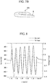
- FIG. 7B shows a pancake coil 101 using the oxide superconductor wire A (B, C) as described above.
- the oxide superconductor wire A may form a wound pancake coil 101. Further, by stacking plural pancake coils 101 and connecting them with one another, it may form a superconductor coil 100 shown in FIG. 7A which will generate strong magnetic force.
- the oxide superconductor wires A, B, and C may be used for various superconductor equipment.
- the superconductor equipment is not particularly limited provided it includes the oxide superconductor wire A, and examples thereof include a superconductor cable, a superconductor motor, a superconductor transformer, a superconductor current-limiting device, and a superconductor electricity storage.
- An Al 2 O 3 layer (diffusion prevention layer; thickness of 150 nm) was formed on a substrate made of tape-shaped HASTELLOY (Trade name, HAYNES INT. INC., USA) having a width of 5 mm and thickness of 0.1 mm by a sputtering method, and a Y 2 O 3 layer (bed layer; thickness of 20 nm) was formed on the diffusion prevention layer by an ion beam sputtering method.
- an MgO layer metal oxide layer; thickness of 10 nm
- IBAD method ion beam assisted deposition method
- CeO 2 cap layer
- PLD method pulse laser deposition method
- a GdBa 2 Cu 3 O 7- ⁇ oxide superconductor layer
- Ag layer protecting layer
- a Sn-solder plated metal tape having a width of 10 mm was folded at both sides of the protection layer to form substantially a C shape in view of the lateral cross section, and the periphery of the oxide superconductor laminate was covered with the metal tape. After that, the Sn solder was melted by heating to form a solder layer such that the metal tape covered and was adhered to the periphery of the oxide superconductor laminate.
- Metal tapes having a thickness and made of a material shown in Table 3 were used.
- the oxide superconductor wires of Examples 1 to 6 and Comparative examples 1 and 2 were subjected to the pressure cooker test in which they were exposed to high temperature (120°C), high humidity (100%), and high pressure (0.2 MPa) for 100 hours, and the ratio of the critical current value before and after the test were measured.
- the percent ratio of the post-exposure critical current value (Ic) to the pre-exposure critical current value (Ic 0 ), which represents moisture derived deterioration is shown in Table 3.
- the metal tape was unable to be formed so as to cover the oxide superconductor laminate in the oxide superconductor wire of Comparative examples 1 and 2. More specifically, as for Comparative example 1, since the thickness 5 ⁇ m of the foil of oxygen free copper used as the metal tape was thin, the metal tape wan torn while forming the metal tape in a C shape and thus the oxide superconductor laminate was unable to be covered.
- the oxide superconductor wires of Comparative examples 1 and 2 were unable to air-tightly cover the oxide superconductor laminate and were thus deteriorated in the pressure cooker test.
- the oxide superconductor wires according to the examples of the present invention exhibited excellent current limiting characteristics. Moreover, in the oxide superconductor wires according to the examples of the present invention, it was confirmed that no moisture derived deterioration occurred even under extreme environmental conditions since the periphery of the oxide superconductor laminate was covered with the metal tape having a certain thickness.
- an oxide superconductor wire for use in superconductor current-limiting devices which is, even if the thickness of the protection layer is reduced, capable of preventing burnout, exhibiting stable current limiting characteristics, and limiting the enlargement of the thickness of the oxide superconductor wire.
Landscapes
- Engineering & Computer Science (AREA)
- Chemical & Material Sciences (AREA)
- Organic Chemistry (AREA)
- Ceramic Engineering (AREA)
- Power Engineering (AREA)
- Inorganic Chemistry (AREA)
- Manufacturing & Machinery (AREA)
- Superconductors And Manufacturing Methods Therefor (AREA)
- Inorganic Compounds Of Heavy Metals (AREA)
- Containers, Films, And Cooling For Superconductive Devices (AREA)
- Emergency Protection Circuit Devices (AREA)
Claims (8)
- Fil supraconducteur en oxyde (A) comprenant :un stratifié supraconducteur en oxyde (1) comprenant : un substrat en forme de bande (3), une couche intermédiaire (4) stratifiée sur le substrat (3), une couche supraconductrice en oxyde (5) stratifiée sur la couche intermédiaire (4), et une couche protectrice (6) formée d'Ag (argent) ou d'un alliage d'Ag et stratifiée sur la couche supraconductrice en oxyde (5) ; etune couche de stabilisation (10) formée d'une bande métallique (2) et formée sur la couche protectrice (6) du stratifié supraconducteur (1) par l'intermédiaire d'une couche de soudure ou de métal à bas point de fusion (7),dans lequel l'épaisseur de la couche protectrice (6) est d'au moins 5 µm,dans lequel l'épaisseur de la couche de stabilisation (10) est d'au moins 9 µm et n'excède pas 60 µm,dans lequel la largeur de la bande métallique (2) constituant la couche de stabilisation (10) est supérieure à la largeur du stratifié supraconducteur en oxyde (1),dans lequel la face supérieure de la couche protectrice (6) du stratifié supraconducteur en oxyde (1) et les faces latérales de la couche protectrice (6), la couche supraconductrice en oxyde (5), la couche intermédiaire (4) et le substrat (3) sont recouverts par la couche de stabilisation (10) par l'intermédiaire de la couche en métal à bas point de fusion (7),dans lequel la bande métallique (2) constituant la couche de stabilisation (10) possède une paroi arrière (2c) à ses deux extrémités,dans lequel les deux parois arrières (2c) s'étendent le long et au-dessus de la face arrière du substrat (3) et recouvrent une partie de la face arrière du substrat (3) par l'intermédiaire de la couche en métal à bas point de fusion (7), etcaractérisé en ce que la couche de soudure (7) comporte une partie de recouvrement (7c) recouvrant dans la largeur les deux extrémités de la bande métallique (2) et dans lequel la résistivité volumique de la couche stabilisation (10) à température ambiante est d'au moins 3,8 µΩ cm et n'excède pas 15 µΩ cm.
- Fil supraconducteur en oxyde (A) selon la revendication 1, dans lequel la valeur de résistance du fil supraconducteur en oxyde (A) pour 1 cm en largeur et 1 cm en longueur à température ambiante est d'au moins 150 µΩ et n'excède pas 100 mΩ.
- Fil supraconducteur en oxyde (A) selon la revendication 1 ou 2,
dans lequel la couche protectrice (6) est formée sur au moins une des faces latérales du substrat (3), de la couche intermédiaire (4), de la couche supraconductrice en oxyde (5), et de la face arrière du substrat (3). - Bobine supraconductrice (100) comprenant le fil supraconducteur en oxyde (A) selon l'une quelconque des revendications 1 à 3.
- Dispositif limiteur de courant supraconducteur (99) comprenant le fil supraconducteur en oxyde (A) selon l'une quelconque des revendications 1 à 3.
- Équipement supraconducteur comprenant le fils supraconducteur en oxyde (1) selon l'une quelconque des revendications 1 à 3.
- Fil supraconducteur en oxyde (A) selon la revendication 1 ou 2, dans lequel, entre les bords distaux des parois arrières (2c), la face arrière du substrat (3) est apparente depuis la couche de stabilisation (10) et la couche en métal à bas point de fusion (7).
- Fil supraconducteur en oxyde (A) selon la revendication 1 ou 2, le fil (A) comprenant en outre une couche enterrée (17c) comblant l'espace entre les bords distaux des parois arrières (2c) de la couche stabilisation (10).
Applications Claiming Priority (2)
| Application Number | Priority Date | Filing Date | Title |
|---|---|---|---|
| JP2012288302 | 2012-12-28 | ||
| PCT/JP2013/084934 WO2014104208A1 (fr) | 2012-12-28 | 2013-12-26 | Fil supraconducteur en oxyde |
Publications (3)
| Publication Number | Publication Date |
|---|---|
| EP2940699A1 EP2940699A1 (fr) | 2015-11-04 |
| EP2940699A4 EP2940699A4 (fr) | 2016-08-17 |
| EP2940699B1 true EP2940699B1 (fr) | 2018-12-05 |
Family
ID=51021282
Family Applications (1)
| Application Number | Title | Priority Date | Filing Date |
|---|---|---|---|
| EP13868560.7A Not-in-force EP2940699B1 (fr) | 2012-12-28 | 2013-12-26 | Fil supraconducteur en oxyde |
Country Status (5)
| Country | Link |
|---|---|
| US (1) | US20150318083A1 (fr) |
| EP (1) | EP2940699B1 (fr) |
| JP (1) | JP5693798B2 (fr) |
| RU (1) | RU2597211C1 (fr) |
| WO (1) | WO2014104208A1 (fr) |
Families Citing this family (4)
| Publication number | Priority date | Publication date | Assignee | Title |
|---|---|---|---|---|
| JP6078522B2 (ja) * | 2014-12-16 | 2017-02-08 | 株式会社フジクラ | 超電導線材及びこれを使用した超電導コイル |
| JP2017117772A (ja) * | 2015-12-18 | 2017-06-29 | 株式会社フジクラ | 酸化物超電導線材の製造方法及び超電導コイルの製造方法 |
| WO2022158413A1 (fr) * | 2021-01-25 | 2022-07-28 | 国立研究開発法人産業技術総合研究所 | Fil supraconducteur à haute température et son procédé de fabrication |
| EP4246602A1 (fr) | 2022-03-14 | 2023-09-20 | Theva Dünnschichttechnik GmbH | Bande supraconductrice à haute température hermétiquement étanche |
Family Cites Families (20)
| Publication number | Priority date | Publication date | Assignee | Title |
|---|---|---|---|---|
| US3964934A (en) * | 1975-05-15 | 1976-06-22 | The Gates Rubber Company | High discharge capability sealed through connector |
| JPH07169343A (ja) * | 1993-10-21 | 1995-07-04 | Sumitomo Electric Ind Ltd | 超電導ケーブル導体 |
| US5851911A (en) * | 1996-03-07 | 1998-12-22 | Micron Technology, Inc. | Mask repattern process |
| JP2954124B2 (ja) * | 1998-01-07 | 1999-09-27 | 株式会社東芝 | 超電導限流素子 |
| US20040266628A1 (en) * | 2003-06-27 | 2004-12-30 | Superpower, Inc. | Novel superconducting articles, and methods for forming and using same |
| US7463915B2 (en) * | 2004-08-20 | 2008-12-09 | American Superconductor Corporation | Stacked filamentary coated superconductors |
| US7816303B2 (en) * | 2004-10-01 | 2010-10-19 | American Superconductor Corporation | Architecture for high temperature superconductor wire |
| US7674751B2 (en) * | 2006-01-10 | 2010-03-09 | American Superconductor Corporation | Fabrication of sealed high temperature superconductor wires |
| DE102006018492A1 (de) * | 2006-04-19 | 2007-10-25 | Tesa Ag | Blasenfrei verklebende Klebeschichten |
| WO2008118127A1 (fr) * | 2006-07-21 | 2008-10-02 | American Superconductor Corporation | Épissure de faible résistance pour des fils supraconducteurs à haute température |
| US20080194411A1 (en) * | 2007-02-09 | 2008-08-14 | Folts Douglas C | HTS Wire |
| JP5403882B2 (ja) * | 2007-07-12 | 2014-01-29 | 株式会社ジェイテクト | モータ制御装置 |
| US8524067B2 (en) * | 2007-07-27 | 2013-09-03 | Nanotek Instruments, Inc. | Electrochemical method of producing nano-scaled graphene platelets |
| US20100019776A1 (en) * | 2008-07-23 | 2010-01-28 | Folts Douglas C | Method for analyzing superconducting wire |
| JP4661966B2 (ja) * | 2009-03-06 | 2011-03-30 | 株式会社デンソー | 電力変換装置 |
| JP2014002833A (ja) * | 2010-09-24 | 2014-01-09 | Fujikura Ltd | 酸化物超電導線材およびその製造方法 |
| JP2012150914A (ja) * | 2011-01-17 | 2012-08-09 | Fujikura Ltd | 高抵抗材複合酸化物超電導線材 |
| JP5684601B2 (ja) | 2011-01-25 | 2015-03-18 | 株式会社フジクラ | 酸化物超電導線材およびその製造方法 |
| EP2490272B1 (fr) * | 2011-02-18 | 2013-08-21 | Bruker HTS GmbH | Élément supraconducteur avec une ouverture allongée et son procédé de fabrication |
| JP5496175B2 (ja) * | 2011-12-27 | 2014-05-21 | 株式会社東芝 | 超電導電流リード |
-
2013
- 2013-12-26 WO PCT/JP2013/084934 patent/WO2014104208A1/fr not_active Ceased
- 2013-12-26 EP EP13868560.7A patent/EP2940699B1/fr not_active Not-in-force
- 2013-12-26 JP JP2014538942A patent/JP5693798B2/ja not_active Expired - Fee Related
- 2013-12-26 US US14/649,991 patent/US20150318083A1/en not_active Abandoned
- 2013-12-26 RU RU2015126603/07A patent/RU2597211C1/ru not_active IP Right Cessation
Non-Patent Citations (1)
| Title |
|---|
| None * |
Also Published As
| Publication number | Publication date |
|---|---|
| EP2940699A1 (fr) | 2015-11-04 |
| JP5693798B2 (ja) | 2015-04-01 |
| EP2940699A4 (fr) | 2016-08-17 |
| US20150318083A1 (en) | 2015-11-05 |
| WO2014104208A1 (fr) | 2014-07-03 |
| JPWO2014104208A1 (ja) | 2017-01-19 |
| RU2597211C1 (ru) | 2016-09-10 |
Similar Documents
| Publication | Publication Date | Title |
|---|---|---|
| CN103959401B (zh) | 氧化物超导电线材及其制造方法、超导电线圈和超导电缆 | |
| EP3179486B1 (fr) | Câble à base d'oxyde supraconducteur, dispositif supraconducteur et procédé de fabrication de câble à base d'oxyde supraconducteur | |
| EP2945168B1 (fr) | Fil supraconducteur d'oxyde, structure de connexion de celui-ci, et dispositif supraconducteur | |
| EP2801983B1 (fr) | Câble supraconducteur, et bobine supraconductrice | |
| EP2958115B1 (fr) | Fil supraconducteur en oxyde | |
| EP2940699A1 (fr) | Fil supraconducteur en oxyde | |
| JP2014220194A (ja) | 酸化物超電導線材及びその製造方法 | |
| JP2014130730A (ja) | 酸化物超電導線材の接続構造体及び接続方法並びに接続構造体を用いた酸化物超電導線材 | |
| JP6101490B2 (ja) | 酸化物超電導線材の接続構造体及び超電導機器 | |
| JP2014154320A (ja) | 酸化物超電導線材の接続構造体及び超電導機器 | |
| JP6069269B2 (ja) | 酸化物超電導線材、超電導機器及び酸化物超電導線材の製造方法 | |
| JP6002602B2 (ja) | 酸化物超電導線材の接続構造体及びその製造方法 | |
| JP2013084382A (ja) | 酸化物超電導線材及びその製造方法 | |
| EP3203483A1 (fr) | Procédé de production de fil supraconducteur oxyde, et procédé de production de bobine supraconductrice | |
| JP6232450B2 (ja) | 酸化物超電導線材 | |
| JPWO2014104333A1 (ja) | 酸化物超電導線材の接続構造体およびその製造方法と超電導機器 | |
| JP2014154331A (ja) | 酸化物超電導線材及び酸化物超電導線材の接続構造体並びに酸化物超電導線材の製造方法 | |
| JP2012209189A (ja) | 酸化物超電導線材及びその製造方法 | |
| JP2014167847A (ja) | 酸化物超電導線材及び超電導コイル並びに酸化物超電導線材の製造方法 | |
| JP2013131397A (ja) | 酸化物超電導線材及びその製造方法 | |
| JP2017010833A (ja) | 酸化物超電導線材および酸化物超電導線材の製造方法 | |
| JP2014022228A (ja) | 酸化物超電導導体および酸化物超電導導体の製造方法並びにそれを用いた超電導機器 |
Legal Events
| Date | Code | Title | Description |
|---|---|---|---|
| PUAI | Public reference made under article 153(3) epc to a published international application that has entered the european phase |
Free format text: ORIGINAL CODE: 0009012 |
|
| 17P | Request for examination filed |
Effective date: 20150610 |
|
| AK | Designated contracting states |
Kind code of ref document: A1 Designated state(s): AL AT BE BG CH CY CZ DE DK EE ES FI FR GB GR HR HU IE IS IT LI LT LU LV MC MK MT NL NO PL PT RO RS SE SI SK SM TR |
|
| AX | Request for extension of the european patent |
Extension state: BA ME |
|
| DAX | Request for extension of the european patent (deleted) | ||
| REG | Reference to a national code |
Ref country code: DE Ref legal event code: R079 Ref document number: 602013047980 Country of ref document: DE Free format text: PREVIOUS MAIN CLASS: H01B0012060000 Ipc: H01L0039140000 |
|
| A4 | Supplementary search report drawn up and despatched |
Effective date: 20160714 |
|
| RIC1 | Information provided on ipc code assigned before grant |
Ipc: H01L 39/14 20060101AFI20160708BHEP Ipc: H01B 12/06 20060101ALI20160708BHEP Ipc: H01F 6/06 20060101ALI20160708BHEP |
|
| STAA | Information on the status of an ep patent application or granted ep patent |
Free format text: STATUS: EXAMINATION IS IN PROGRESS |
|
| 17Q | First examination report despatched |
Effective date: 20170320 |
|
| GRAP | Despatch of communication of intention to grant a patent |
Free format text: ORIGINAL CODE: EPIDOSNIGR1 |
|
| STAA | Information on the status of an ep patent application or granted ep patent |
Free format text: STATUS: GRANT OF PATENT IS INTENDED |
|
| INTG | Intention to grant announced |
Effective date: 20180712 |
|
| GRAS | Grant fee paid |
Free format text: ORIGINAL CODE: EPIDOSNIGR3 |
|
| GRAA | (expected) grant |
Free format text: ORIGINAL CODE: 0009210 |
|
| STAA | Information on the status of an ep patent application or granted ep patent |
Free format text: STATUS: THE PATENT HAS BEEN GRANTED |
|
| AK | Designated contracting states |
Kind code of ref document: B1 Designated state(s): AL AT BE BG CH CY CZ DE DK EE ES FI FR GB GR HR HU IE IS IT LI LT LU LV MC MK MT NL NO PL PT RO RS SE SI SK SM TR |
|
| REG | Reference to a national code |
Ref country code: GB Ref legal event code: FG4D |
|
| REG | Reference to a national code |
Ref country code: CH Ref legal event code: EP |
|
| REG | Reference to a national code |
Ref country code: AT Ref legal event code: REF Ref document number: 1074155 Country of ref document: AT Kind code of ref document: T Effective date: 20181215 |
|
| REG | Reference to a national code |
Ref country code: IE Ref legal event code: FG4D |
|
| REG | Reference to a national code |
Ref country code: DE Ref legal event code: R096 Ref document number: 602013047980 Country of ref document: DE |
|
| PGFP | Annual fee paid to national office [announced via postgrant information from national office to epo] |
Ref country code: DE Payment date: 20181211 Year of fee payment: 6 |
|
| REG | Reference to a national code |
Ref country code: NL Ref legal event code: MP Effective date: 20181205 |
|
| REG | Reference to a national code |
Ref country code: AT Ref legal event code: MK05 Ref document number: 1074155 Country of ref document: AT Kind code of ref document: T Effective date: 20181205 |
|
| REG | Reference to a national code |
Ref country code: LT Ref legal event code: MG4D |
|
| PG25 | Lapsed in a contracting state [announced via postgrant information from national office to epo] |
Ref country code: BG Free format text: LAPSE BECAUSE OF FAILURE TO SUBMIT A TRANSLATION OF THE DESCRIPTION OR TO PAY THE FEE WITHIN THE PRESCRIBED TIME-LIMIT Effective date: 20190305 Ref country code: LT Free format text: LAPSE BECAUSE OF FAILURE TO SUBMIT A TRANSLATION OF THE DESCRIPTION OR TO PAY THE FEE WITHIN THE PRESCRIBED TIME-LIMIT Effective date: 20181205 Ref country code: FI Free format text: LAPSE BECAUSE OF FAILURE TO SUBMIT A TRANSLATION OF THE DESCRIPTION OR TO PAY THE FEE WITHIN THE PRESCRIBED TIME-LIMIT Effective date: 20181205 Ref country code: NO Free format text: LAPSE BECAUSE OF FAILURE TO SUBMIT A TRANSLATION OF THE DESCRIPTION OR TO PAY THE FEE WITHIN THE PRESCRIBED TIME-LIMIT Effective date: 20190305 Ref country code: LV Free format text: LAPSE BECAUSE OF FAILURE TO SUBMIT A TRANSLATION OF THE DESCRIPTION OR TO PAY THE FEE WITHIN THE PRESCRIBED TIME-LIMIT Effective date: 20181205 Ref country code: HR Free format text: LAPSE BECAUSE OF FAILURE TO SUBMIT A TRANSLATION OF THE DESCRIPTION OR TO PAY THE FEE WITHIN THE PRESCRIBED TIME-LIMIT Effective date: 20181205 Ref country code: ES Free format text: LAPSE BECAUSE OF FAILURE TO SUBMIT A TRANSLATION OF THE DESCRIPTION OR TO PAY THE FEE WITHIN THE PRESCRIBED TIME-LIMIT Effective date: 20181205 Ref country code: AT Free format text: LAPSE BECAUSE OF FAILURE TO SUBMIT A TRANSLATION OF THE DESCRIPTION OR TO PAY THE FEE WITHIN THE PRESCRIBED TIME-LIMIT Effective date: 20181205 |
|
| PG25 | Lapsed in a contracting state [announced via postgrant information from national office to epo] |
Ref country code: GR Free format text: LAPSE BECAUSE OF FAILURE TO SUBMIT A TRANSLATION OF THE DESCRIPTION OR TO PAY THE FEE WITHIN THE PRESCRIBED TIME-LIMIT Effective date: 20190306 Ref country code: RS Free format text: LAPSE BECAUSE OF FAILURE TO SUBMIT A TRANSLATION OF THE DESCRIPTION OR TO PAY THE FEE WITHIN THE PRESCRIBED TIME-LIMIT Effective date: 20181205 Ref country code: SE Free format text: LAPSE BECAUSE OF FAILURE TO SUBMIT A TRANSLATION OF THE DESCRIPTION OR TO PAY THE FEE WITHIN THE PRESCRIBED TIME-LIMIT Effective date: 20181205 Ref country code: AL Free format text: LAPSE BECAUSE OF FAILURE TO SUBMIT A TRANSLATION OF THE DESCRIPTION OR TO PAY THE FEE WITHIN THE PRESCRIBED TIME-LIMIT Effective date: 20181205 |
|
| PG25 | Lapsed in a contracting state [announced via postgrant information from national office to epo] |
Ref country code: NL Free format text: LAPSE BECAUSE OF FAILURE TO SUBMIT A TRANSLATION OF THE DESCRIPTION OR TO PAY THE FEE WITHIN THE PRESCRIBED TIME-LIMIT Effective date: 20181205 |
|
| PG25 | Lapsed in a contracting state [announced via postgrant information from national office to epo] |
Ref country code: IT Free format text: LAPSE BECAUSE OF FAILURE TO SUBMIT A TRANSLATION OF THE DESCRIPTION OR TO PAY THE FEE WITHIN THE PRESCRIBED TIME-LIMIT Effective date: 20181205 Ref country code: PT Free format text: LAPSE BECAUSE OF FAILURE TO SUBMIT A TRANSLATION OF THE DESCRIPTION OR TO PAY THE FEE WITHIN THE PRESCRIBED TIME-LIMIT Effective date: 20190405 Ref country code: CZ Free format text: LAPSE BECAUSE OF FAILURE TO SUBMIT A TRANSLATION OF THE DESCRIPTION OR TO PAY THE FEE WITHIN THE PRESCRIBED TIME-LIMIT Effective date: 20181205 Ref country code: PL Free format text: LAPSE BECAUSE OF FAILURE TO SUBMIT A TRANSLATION OF THE DESCRIPTION OR TO PAY THE FEE WITHIN THE PRESCRIBED TIME-LIMIT Effective date: 20181205 |
|
| REG | Reference to a national code |
Ref country code: CH Ref legal event code: PL |
|
| PG25 | Lapsed in a contracting state [announced via postgrant information from national office to epo] |
Ref country code: LU Free format text: LAPSE BECAUSE OF NON-PAYMENT OF DUE FEES Effective date: 20181226 Ref country code: IS Free format text: LAPSE BECAUSE OF FAILURE TO SUBMIT A TRANSLATION OF THE DESCRIPTION OR TO PAY THE FEE WITHIN THE PRESCRIBED TIME-LIMIT Effective date: 20190405 Ref country code: SK Free format text: LAPSE BECAUSE OF FAILURE TO SUBMIT A TRANSLATION OF THE DESCRIPTION OR TO PAY THE FEE WITHIN THE PRESCRIBED TIME-LIMIT Effective date: 20181205 Ref country code: RO Free format text: LAPSE BECAUSE OF FAILURE TO SUBMIT A TRANSLATION OF THE DESCRIPTION OR TO PAY THE FEE WITHIN THE PRESCRIBED TIME-LIMIT Effective date: 20181205 Ref country code: SM Free format text: LAPSE BECAUSE OF FAILURE TO SUBMIT A TRANSLATION OF THE DESCRIPTION OR TO PAY THE FEE WITHIN THE PRESCRIBED TIME-LIMIT Effective date: 20181205 Ref country code: EE Free format text: LAPSE BECAUSE OF FAILURE TO SUBMIT A TRANSLATION OF THE DESCRIPTION OR TO PAY THE FEE WITHIN THE PRESCRIBED TIME-LIMIT Effective date: 20181205 |
|
| REG | Reference to a national code |
Ref country code: DE Ref legal event code: R097 Ref document number: 602013047980 Country of ref document: DE |
|
| REG | Reference to a national code |
Ref country code: IE Ref legal event code: MM4A |
|
| REG | Reference to a national code |
Ref country code: BE Ref legal event code: MM Effective date: 20181231 |
|
| PLBE | No opposition filed within time limit |
Free format text: ORIGINAL CODE: 0009261 |
|
| STAA | Information on the status of an ep patent application or granted ep patent |
Free format text: STATUS: NO OPPOSITION FILED WITHIN TIME LIMIT |
|
| PG25 | Lapsed in a contracting state [announced via postgrant information from national office to epo] |
Ref country code: DK Free format text: LAPSE BECAUSE OF FAILURE TO SUBMIT A TRANSLATION OF THE DESCRIPTION OR TO PAY THE FEE WITHIN THE PRESCRIBED TIME-LIMIT Effective date: 20181205 Ref country code: SI Free format text: LAPSE BECAUSE OF FAILURE TO SUBMIT A TRANSLATION OF THE DESCRIPTION OR TO PAY THE FEE WITHIN THE PRESCRIBED TIME-LIMIT Effective date: 20181205 Ref country code: MC Free format text: LAPSE BECAUSE OF FAILURE TO SUBMIT A TRANSLATION OF THE DESCRIPTION OR TO PAY THE FEE WITHIN THE PRESCRIBED TIME-LIMIT Effective date: 20181205 Ref country code: IE Free format text: LAPSE BECAUSE OF NON-PAYMENT OF DUE FEES Effective date: 20181226 |
|
| 26N | No opposition filed |
Effective date: 20190906 |
|
| GBPC | Gb: european patent ceased through non-payment of renewal fee |
Effective date: 20190305 |
|
| PG25 | Lapsed in a contracting state [announced via postgrant information from national office to epo] |
Ref country code: BE Free format text: LAPSE BECAUSE OF NON-PAYMENT OF DUE FEES Effective date: 20181231 |
|
| PG25 | Lapsed in a contracting state [announced via postgrant information from national office to epo] |
Ref country code: CH Free format text: LAPSE BECAUSE OF NON-PAYMENT OF DUE FEES Effective date: 20181231 Ref country code: LI Free format text: LAPSE BECAUSE OF NON-PAYMENT OF DUE FEES Effective date: 20181231 |
|
| PG25 | Lapsed in a contracting state [announced via postgrant information from national office to epo] |
Ref country code: MT Free format text: LAPSE BECAUSE OF NON-PAYMENT OF DUE FEES Effective date: 20181226 Ref country code: GB Free format text: LAPSE BECAUSE OF NON-PAYMENT OF DUE FEES Effective date: 20190305 |
|
| PG25 | Lapsed in a contracting state [announced via postgrant information from national office to epo] |
Ref country code: FR Free format text: LAPSE BECAUSE OF NON-PAYMENT OF DUE FEES Effective date: 20190205 |
|
| PG25 | Lapsed in a contracting state [announced via postgrant information from national office to epo] |
Ref country code: TR Free format text: LAPSE BECAUSE OF FAILURE TO SUBMIT A TRANSLATION OF THE DESCRIPTION OR TO PAY THE FEE WITHIN THE PRESCRIBED TIME-LIMIT Effective date: 20181205 |
|
| PG25 | Lapsed in a contracting state [announced via postgrant information from national office to epo] |
Ref country code: HU Free format text: LAPSE BECAUSE OF FAILURE TO SUBMIT A TRANSLATION OF THE DESCRIPTION OR TO PAY THE FEE WITHIN THE PRESCRIBED TIME-LIMIT; INVALID AB INITIO Effective date: 20131226 Ref country code: CY Free format text: LAPSE BECAUSE OF FAILURE TO SUBMIT A TRANSLATION OF THE DESCRIPTION OR TO PAY THE FEE WITHIN THE PRESCRIBED TIME-LIMIT Effective date: 20181205 Ref country code: MK Free format text: LAPSE BECAUSE OF NON-PAYMENT OF DUE FEES Effective date: 20181205 |
|
| REG | Reference to a national code |
Ref country code: DE Ref legal event code: R119 Ref document number: 602013047980 Country of ref document: DE |
|
| PG25 | Lapsed in a contracting state [announced via postgrant information from national office to epo] |
Ref country code: DE Free format text: LAPSE BECAUSE OF NON-PAYMENT OF DUE FEES Effective date: 20200701 |