EP1006569A2 - Abscheidung eines isolierenden Films - Google Patents
Abscheidung eines isolierenden Films Download PDFInfo
- Publication number
- EP1006569A2 EP1006569A2 EP99114234A EP99114234A EP1006569A2 EP 1006569 A2 EP1006569 A2 EP 1006569A2 EP 99114234 A EP99114234 A EP 99114234A EP 99114234 A EP99114234 A EP 99114234A EP 1006569 A2 EP1006569 A2 EP 1006569A2
- Authority
- EP
- European Patent Office
- Prior art keywords
- film
- phosphorus
- gas
- insulating film
- oxygen
- Prior art date
- Legal status (The legal status is an assumption and is not a legal conclusion. Google has not performed a legal analysis and makes no representation as to the accuracy of the status listed.)
- Withdrawn
Links
Images






Classifications
-
- H—ELECTRICITY
- H10—SEMICONDUCTOR DEVICES; ELECTRIC SOLID-STATE DEVICES NOT OTHERWISE PROVIDED FOR
- H10P—GENERIC PROCESSES OR APPARATUS FOR THE MANUFACTURE OR TREATMENT OF DEVICES COVERED BY CLASS H10
- H10P14/00—Formation of materials, e.g. in the shape of layers or pillars
- H10P14/60—Formation of materials, e.g. in the shape of layers or pillars of insulating materials
-
- H—ELECTRICITY
- H10—SEMICONDUCTOR DEVICES; ELECTRIC SOLID-STATE DEVICES NOT OTHERWISE PROVIDED FOR
- H10P—GENERIC PROCESSES OR APPARATUS FOR THE MANUFACTURE OR TREATMENT OF DEVICES COVERED BY CLASS H10
- H10P14/00—Formation of materials, e.g. in the shape of layers or pillars
- H10P14/60—Formation of materials, e.g. in the shape of layers or pillars of insulating materials
- H10P14/69—Inorganic materials
- H10P14/692—Inorganic materials composed of oxides, glassy oxides or oxide-based glasses
- H10P14/6921—Inorganic materials composed of oxides, glassy oxides or oxide-based glasses containing silicon
- H10P14/6922—Inorganic materials composed of oxides, glassy oxides or oxide-based glasses containing silicon the material containing Si, O and at least one of H, N, C, F or other non-metal elements, e.g. SiOC, SiOC:H or SiONC
- H10P14/6923—Inorganic materials composed of oxides, glassy oxides or oxide-based glasses containing silicon the material containing Si, O and at least one of H, N, C, F or other non-metal elements, e.g. SiOC, SiOC:H or SiONC the material being boron or phosphorus doped silicon oxides, e.g. BPSG, BSG or PSG
-
- C—CHEMISTRY; METALLURGY
- C23—COATING METALLIC MATERIAL; COATING MATERIAL WITH METALLIC MATERIAL; CHEMICAL SURFACE TREATMENT; DIFFUSION TREATMENT OF METALLIC MATERIAL; COATING BY VACUUM EVAPORATION, BY SPUTTERING, BY ION IMPLANTATION OR BY CHEMICAL VAPOUR DEPOSITION, IN GENERAL; INHIBITING CORROSION OF METALLIC MATERIAL OR INCRUSTATION IN GENERAL
- C23C—COATING METALLIC MATERIAL; COATING MATERIAL WITH METALLIC MATERIAL; SURFACE TREATMENT OF METALLIC MATERIAL BY DIFFUSION INTO THE SURFACE, BY CHEMICAL CONVERSION OR SUBSTITUTION; COATING BY VACUUM EVAPORATION, BY SPUTTERING, BY ION IMPLANTATION OR BY CHEMICAL VAPOUR DEPOSITION, IN GENERAL
- C23C16/00—Chemical coating by decomposition of gaseous compounds, without leaving reaction products of surface material in the coating, i.e. chemical vapour deposition [CVD] processes
- C23C16/22—Chemical coating by decomposition of gaseous compounds, without leaving reaction products of surface material in the coating, i.e. chemical vapour deposition [CVD] processes characterised by the deposition of inorganic material, other than metallic material
- C23C16/30—Deposition of compounds, mixtures or solid solutions, e.g. borides, carbides, nitrides
- C23C16/40—Oxides
- C23C16/401—Oxides containing silicon
-
- H—ELECTRICITY
- H10—SEMICONDUCTOR DEVICES; ELECTRIC SOLID-STATE DEVICES NOT OTHERWISE PROVIDED FOR
- H10P—GENERIC PROCESSES OR APPARATUS FOR THE MANUFACTURE OR TREATMENT OF DEVICES COVERED BY CLASS H10
- H10P14/00—Formation of materials, e.g. in the shape of layers or pillars
- H10P14/60—Formation of materials, e.g. in the shape of layers or pillars of insulating materials
- H10P14/65—Formation of materials, e.g. in the shape of layers or pillars of insulating materials characterised by treatments performed before or after the formation of the materials
- H10P14/6516—Formation of materials, e.g. in the shape of layers or pillars of insulating materials characterised by treatments performed before or after the formation of the materials of treatments performed after formation of the materials
- H10P14/6529—Formation of materials, e.g. in the shape of layers or pillars of insulating materials characterised by treatments performed before or after the formation of the materials of treatments performed after formation of the materials by exposure to a gas or vapour
-
- H—ELECTRICITY
- H10—SEMICONDUCTOR DEVICES; ELECTRIC SOLID-STATE DEVICES NOT OTHERWISE PROVIDED FOR
- H10P—GENERIC PROCESSES OR APPARATUS FOR THE MANUFACTURE OR TREATMENT OF DEVICES COVERED BY CLASS H10
- H10P14/00—Formation of materials, e.g. in the shape of layers or pillars
- H10P14/60—Formation of materials, e.g. in the shape of layers or pillars of insulating materials
- H10P14/66—Formation of materials, e.g. in the shape of layers or pillars of insulating materials characterised by the type of materials
- H10P14/668—Formation of materials, e.g. in the shape of layers or pillars of insulating materials characterised by the type of materials the materials being characterised by the deposition precursor materials
- H10P14/6681—Formation of materials, e.g. in the shape of layers or pillars of insulating materials characterised by the type of materials the materials being characterised by the deposition precursor materials the precursor containing a compound comprising Si
- H10P14/6684—Formation of materials, e.g. in the shape of layers or pillars of insulating materials characterised by the type of materials the materials being characterised by the deposition precursor materials the precursor containing a compound comprising Si the compound comprising silicon and oxygen
- H10P14/6686—Formation of materials, e.g. in the shape of layers or pillars of insulating materials characterised by the type of materials the materials being characterised by the deposition precursor materials the precursor containing a compound comprising Si the compound comprising silicon and oxygen the compound being a molecule comprising at least one silicon-oxygen bond and the compound having hydrogen or an organic group attached to the silicon or oxygen, e.g. a siloxane
-
- H—ELECTRICITY
- H10—SEMICONDUCTOR DEVICES; ELECTRIC SOLID-STATE DEVICES NOT OTHERWISE PROVIDED FOR
- H10P—GENERIC PROCESSES OR APPARATUS FOR THE MANUFACTURE OR TREATMENT OF DEVICES COVERED BY CLASS H10
- H10P14/00—Formation of materials, e.g. in the shape of layers or pillars
- H10P14/60—Formation of materials, e.g. in the shape of layers or pillars of insulating materials
- H10P14/63—Formation of materials, e.g. in the shape of layers or pillars of insulating materials characterised by the formation processes
- H10P14/6326—Deposition processes
- H10P14/6328—Deposition from the gas or vapour phase
- H10P14/6334—Deposition from the gas or vapour phase using decomposition or reaction of gaseous or vapour phase compounds, i.e. chemical vapour deposition
- H10P14/6336—Deposition from the gas or vapour phase using decomposition or reaction of gaseous or vapour phase compounds, i.e. chemical vapour deposition in the presence of a plasma [PECVD]
Definitions
- the present invention relates to a method of forming a flattened interlayer insulating film covering a wiring layer of a semiconductor integrated circuit, and a method of manufacturing a semiconductor device.
- a multi-layer wiring including several layers is formed within the semiconductor integrated circuit. Since the wiring layer is formed of aluminum in many cases, a strong demand has been directed to the development of a method of forming a flattened interlayer insulating film at a low temperature, e.g., 500 °C or less.
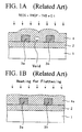
- FIG. 1 shows a related method of flattening an insulating film.
- a phosphorus-containing insulating film is formed by a thermal CVD (Chemical Vapor Deposition) method or a plasma-enhanced CVD method, followed by heating the phosphorus-containing insulating film so as to fluidize and flatten the insulating film.
- etch back method shown in FIG. 2
- CMP Chemical Mechanical Polishing
- a BPSG film 4 is formed as shown in FIG. 1A by using any of the reactant gases below.
- any group of the reactant gases given below are used:
- any group of the following reactant gases are employed.
- the formed BPSG film 4 is heated at a temperature of about 850 °C, as shown in FIG. 1B, to fluidize and flatten the film 4.
- the film is formed by the thermal CVD method or the plasma-enhanced CVD method using a reactant gas other than the boron-containing gases (B 2 H 6 , TMB or TEB) among the above described reactant gases, and then the film is heated at a temperature below 1000 °C to fluidize and flatten the film.
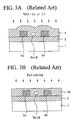
- an NSG film (Nondoped Silicate Glass film) 5 is first formed by the thermal CVD method or the plasma-enhanced CVD method using the following reactant gases as shown in FIGS. 2A and 3A, and then the film is flattened.
- the resist film 6 is formed on the NSG film 5 by a spin coating method, followed by flattening the resist film 6. Then, as shown in FIG. 2C, the film is subjected to an etching that is performed from the upper portion of the film 5, thus forming the flattened NSG film 5a. Moreover, in the CMP method, as shown in FIG. 3B the NSG film 5 is formed and, then polished to obtain the flattened NSG film 5b.
- reference numeral 1 denotes a semiconductor substrate.
- Reference numeral 2 denotes an underlying insulating film.
- each of reference numerals 3a and 3b denotes a wiring layer formed on the underlying insulating film 2.
- the film is not heated unlike the flattening method utilizing thermal fluidization.
- the etch-back method and the CMP method are effective in case that flattening of the film must be performed especially at a low temperature. Nevertheless, when voids are formed in concave portions between the wiring layers 3a and 3b and in the other concave portions immediately after the formation of the original insulating film 5, these voids remain as they were even after the flattening treatment as shown in FIGS. 2 and 3.
- Methods of forming the insulating film providing a good burying property includes, for example, a high density plasma-enhanced CVD method, a ordinary plasma-enhanced CVD method, a normal pressure thermal CVD method, and an SOG (Spin-On-Glass) coating method.
- a high density plasma-enhanced CVD method a high density plasma-enhanced CVD method
- a ordinary plasma-enhanced CVD method a normal pressure thermal CVD method
- SOG Spin-On-Glass
- the film surface flattening method in which the film is flattened by heating and fluidizing the film utilizes the thermal fluidity of the film, it can be expected that the concave portion can be perfectly buried as shown in FIG. 1.
- the BPSG film (boro-phospho silicate glass film) 4 is often used for such a purpose.
- the BPSG film 4 in order to fluidize the BPSG film 4, the BPSG film 4 must be heated at least at a temperature higher than 850 °C, and this BPSG film cannot be applicable to such a use as the underlying film of the wiring layers 3a and 3b as well as the interlayer insulating film 4, which must be formed at a low temperature.
- a temperature for fluidizing the film (hereinafter referred to as a fluidizing temperature) can be decreased to some extent.
- a fluidizing temperature a temperature for fluidizing the film
- a GBPSG film obtained by adding GeO 2 to the BPSG film has been developed.
- the fluidizing temperature cannot be decreased only about 750 °C, and it is difficult to apply the BPSG film to the underlying film and the interlayer insulating film which requires a lower fluidizing temperature.
- the object of the present invention is to provide a film-forming formation method which is capable of significantly decreasing the fluidizing temperature for flattening a film, and a method of manufacturing a semiconductor device.
- the inventors of the present invention paid their attentions to the following facts.
- the inventors thought that the fluidizing temperature could be decreased if the BPSG film and the PSG film are made to mainly contain P 2 O 3 instead of P 2 O 5 .
- the inventors intended to oxidize a phosphorus-containing compound under the state of oxygen shortage.
- the following items are conceived: (1) the phosphorus-containing compound that contains trivalent phosphorus is used as a film formation gas, and (2) the film formation is conducted using a silicon-containing compound containing a small amount of oxygen and a phosphorus-containing compound.
- the phosphorus-containing compound applicable to the method (1) or (2) for example, it is possible to use a phosphorus-containing compound having a Si-O-P structure as shown in the following structural formulae.
- silicon-containing compound applicable to method (2) there is a silicon-containing compound containing at most one atom, for example, hexamethyldisiloxane (HMDSO) and the like.
- HMDSO hexamethyldisiloxane
- a film-forming gas formed of only a phosphorus-containing compound and a silicon-containing compound in which an oxidative gas is not added.
- This film-forming gas contains carrier gases of these compounds.
- the oxidative gas is not added to the film-forming gas, a film-forming rate decreases.
- the oxidative gas e.g., O 2 gas
- the oxidative gas should be added in amount of, for example, 15 sccm or less, more suitably 10 sccm or less, if possible, such that the state of oxygen shortage can be maintained to permit a trivalent phosphorus component to be contained in the phosphorus-containing insulating film and that the film-forming rate of a reasonable level can be maintained.
- the phosphorus-containing insulating film for example, the PSG film, the BPSG film and the like, was formed by a plasma-enhanced CVD method.
- the components of this phosphorus-containing insulating film is analyzed by a Fourier transformation infrared specrophotometric (FTIR) method, it can be confirmed that P 2 O 3 of a high concentration exists in the phosphorus insulating film. Then, the fluidizing temperature approximately identical to the film formation temperature of about 240 to 430 °C was achieved.
- FTIR Fourier transformation infrared specrophotometric
- the fluidizing temperature can be adjusted by adjusting the concentration of P 2 O 3 . It was also found that the concentration of P 2 O 3 can be easily adjusted by adjusting the film formation temperature, the oxygen concentration and the gas flow rate of the phosphorus-containing compound.
- a phosphorus-containing compound having a Si-O-P structure of the structural formula shown below phosphorus acid dimethyl trimethylsilylester (hereinafter, referred to as an SOP-11(a)) and phosphorus acid dimethoxy trimethylsilylester (hereinafter, referred to as an SOP-11 (b)) can be used.
- SOP-11 (a) phosphorus acid dimethyl trimethylsilylester
- SOP-11 (b) phosphorus acid dimethoxy trimethylsilylester
- the structural formula of the SOP-11 (a) is as follows.
- the structural formula of the SOP-11 (b) is as follows. Hereupon, the SOP-11 (b) was used.
- R denotes an alkyl group, an aryl group or their derivative, and n is zero or a positive integer.
- HMDSO hexamethyldisiloxane
- TEOS hexamethyldisiloxane
- the reason is that hexamethyldisiloxane is chemically stable and not prone to react with water because of the small numbers of carbon atoms and hydrogen atoms contained therein.
- the number of oxygen atoms contained in hexamethyldisiloxane is small, with the result that the state of oxygen shortage during the film formation can easily be obtained, resulting in a high P 2 O 3 content in the grown film.
- oxygen oxygen (O 2 ), carbon monoxide (CO), carbon dioxide (CO 2 ), nitride monoxide (NO), nitrous oxide (N 2 O), nitride dioxide (NO 2 ) and the like can be used.
- O 2 is used.
- the oxidative gas may not be added. However, if the oxidative gas is not added, the film-forming rate decreases. For this reason, the oxidative gas should be added at an appropriate amount.
- oxygen O 2 gas should be added in an amount of 15 sccm or less, more suitably 10 sccm or less if possible, such that the state of oxygen shortage can be maintained to a degree that trivalent phosphorus is contained in the phosphorus-containing insulating film and the film-forming rate can be maintained to some extent.
- mixed gas composed of SOP-11(b), HMDSO and O 2 is used as the film-forming gas, and the film-forming conditions should be as follows.
- Substrate Temperature 150 to 250°C Gas Pressure: 2 to 10 Torr
- Flow Rate of HMDSO Bubbling Gas (N 2 or Ar) 200 to 600 sccm
- HMDSO Source Temperature: 10°C Flow Rate of Oxidative Gas (O 2 ): below 15 sccm
- RF Power 150 to 300 W Frequency: 380 kHZ to 2.45 GHZ
- SOP-11(b) was heated to 45 °C and HMDSO was cooled to 10 °C. Then, these liquid sources were bubbled with carrier gas (N 2 or Ar) so as to mix it into the carrier gas. By adjusting the flow rate of the carrier gas, the supply amount of SOP-11(b) and HMDSO was adjusted.
- carrier gas N 2 or Ar
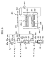
- the film formation apparatus 301 comprises the upper electrode 203 and the lower electrode 202 of a parallel plane type in the chamber 201.
- the RF power source 207 is connected between the upper and lower electrodes 203 and 202.
- the RF power source 207 supplies a RF power of a frequency of 13.56 MHz to convert the film-forming gas into a plasma.
- a pressure in the chamber 201 is reduced to an appropriate value by exhausting the air from the chamber 201 using an exhaustion apparatus connected to the exhaustion port 205.
- the lower electrode 202 serves also as a substrate placing stage for placing the substrate 101 on which the film is to be formed (hereinafter referred to as a substrate 101).
- the heating means 206 for heating the substrate 101 is provided in the vicinity of the lower electrode 202.
- the supply source 21 of SOP-11(b) is provided as the phosphorus-containing compound source 33; the supply source 22 of HMDSO, as the silicon-containing compound source 36; the supply source of O 2 , as the oxidative gas; and the supply source of He, Ar or N 2 , as the diluent gas source.
- the supply sources are collectively connected to the gas inlet portion 204 of the chamber 201 of the film formation apparatus 301 through the pipe 24.
- RF power source 207 is connected to the upper electrode 203 through the matching circuit 208.
- other reference numerals 24a to 24d denote a pipe for guiding each gas.
- Reference numerals 25a to 25d denote a flow meter, and reference numerals 26a and 26b denote a valve for opening and closing the flowing path of the source gas provided in the pipes 24a to 24d.
- Reference numerals 32 and 35 denote means for adjusting the temperature of the source, which are a heater, a cooler and the like.
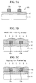
- the substrate 101 shown in FIG. 4A, on which the film is to be formed is introduced into the chamber 201 of the PECVD apparatus constructed as described above. Subsequently, the substrate 101 is heated to maintain the temperature of the substrate within the range of the Table 2.
- the substrate 101 on which the film is to be formed is constructed such that the underlying insulating film 12 such as a silicon oxide film is formed on the silicon substrate (semiconductor substrate) 11, and the wiring layer 13 formed of, for example, an aluminum film is formed on the underlying insulating film 12.
- the underlying insulating film 12 such as a silicon oxide film is formed on the silicon substrate (semiconductor substrate) 11, and the wiring layer 13 formed of, for example, an aluminum film is formed on the underlying insulating film 12.
- the film-forming gas which was controlled so as to fall within the range of the film formation condition shown in FIG. 2 is introduced into the chamber 201, and the film-forming gas is converted into plasma by the RF power of the Table 2, thereby activating it.
- the PSG film (phosphorus-containing insulating film) 14 of a predetermined thickness containing a high concentration of P 2 O 3 is formed.
- the fluidizing temperature of the PSG film 14 can be controlled so as to fall within a range of 200 to 500°C.
- the PSG film 14 may be fluidized, so that the formation of the film and flattening of the film can be achieved in this case.
- the PSG film (phosphorus-containing insulating film) 15 is formed on the substrate 101 as shown in FIGS. 5A to 5C, and then a thermal treatment for flattening the film 15 is conducted, thereby fluidizing the film 15. Thus, the film 15 is flattened. With such processings, the flattened PSG film 15a is formed.
- FIG. 9 is a graph showing a dependency of the film-forming rate on the RF power in the PECVD method.
- the ordinate on the left side of FIG. 9 shows the film-forming rate ( ⁇ /min.) illustrated by linear scales, and the abscissa shows the RF power (W) illustrated by the linear scales.
- the film-forming conditions of the sample used for the investigation are as follows. Substrate Temperature: 170 °C Gas Pressure: 10 Torr Total Gas Flow Rate: 940 sccm SiOP-11(b)/ HMDSO Flow Rate(Ar Carrier Gas) : 1.6 ( SiOP-11(b) Source Temperature : 45 °C HMDSO Source Temperature: 10 °C ) Flow Rate of Oxidative Gas (O 2 ): 1 to 15 sccm RF power: 200 to 350 W Frequency: 13.56MHz
- the film-forming rate can be increased to about 40 to 60 % compared to the case where oxygen is not added, while securing the situation of oxygen shortage.
- the contraction rate is defined by a ratio (%) of the film thickness after annealing to the film thickness before annealing, that is, (the film thickness after annealing)/ (the film thickness before annealing) ⁇ 100 .
- the ordinate on the right side of FIG. 9 shows the contraction rate (%) of the phosphorus-containing insulating film, which is expressed by the linear scales, and the abscissa shows the RF power (W) expressed by the linear scales.
- hexamethyldisiloxane (HMDSO) having one oxygen atom or less is used as the silicon-containing compound
- SiOP-11 (b) is used as the phosphorus-containing compound
- the oxidative gas e.g., O 2 gas, is added in a suitable amount of 15 sccm or less.
- the amount of oxygen in the total film-forming gas can be decreased, and the PSG film 15 containing a high concentration of P 2 O 3 can be formed. Therefore, the fluidizing temperature can be decreased to 500 °C or less.
- oxygen (O 2 ) is added as the oxidative gas by an appropriate amount, that is, by 15 sccm or less, the film-forming rate of a reasonable level can be maintained.
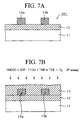
- FIGS. 7A and 7B a formation method of a BPSG film containing P 2 O 3 by a plasma-enhanced CVD method according to a second embodiment of the present invention will be described with reference to FIGS. 7A and 7B.
- a mixed gas containing HMDSO + SOP-11(b) + TMB or TEB + O 2 was used as the film-forming gas.
- the film-forming conditions were as follows. Substrate Temperature: 150 to 250°C Gas Pressure : 2 to 10 Torr Flow Rate of SiOP-11(b) Bubbling Gas (N 2 or Ar): 300 to 800 sccm (SiOP-11 (b) Source Temperature: 45°C) Flow Rate of HMDSO Bubbling Gas (N 2 or Ar): 200 to 600 sccm (HMDSO Source Temperature: 10°C) TMP Flow Rate: 5 to 200 sccm TMB or TEB Flow Rate: 3 to 400 sccm Oxidative Gas (O 2 ) Flow Rate : 15 sccm or less RF power: 150 to 300 W Frequency: 380 kHz to 2.45 GHz
- the BPSG film (phosphorus-containing insulating film) 17 formed of the mixture containing SiO 2 + P 2 O 3 + B 2 O 3 is formed on the substrate 101 as shown in FIG. 7B.
- FIG. 7A shows a sectional view of the substrate 101 before the film formation.
- the concentration of P 2 O 3 or the ratio of P 2 O 3 /P 2 O 5 is controlled by controlling the oxygen concentration, the substrate temperature, the phosphorus-containing compound or the boron-containing compound.
- the fluizing temperature of the BPSG film 17 can be controlled so as to fall within a range of 200 to 500 °C.
- oxygen (O 2 ) is added as the oxidative gas in an appropriate amount, that is, 15 sccm or less, a reasonable film-forming rate can be maintained.
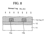
- a substrate on which the film was formed is introduced into the chamber, and the substrate is heated to a temperature of 650 °C.
- N 2 is introduced into the chamber, and annealing is performed for about 15 minutes at the substrate temperature of 650 °C in an atmosphere of nitrogen. Subsequently, the introduction of nitrogen into the chamber is stopped, and oxygen is introduced into the chamber, followed by annealing the substrate for about 15 minutes at the substrate temperature of 650 °C in an atmosphere of nitrogen.
- P 2 O 3 contained in the PSG films 14 and 15a and the BPSG film 17 can be converted into P 2 O 5 .
- annealing is performed in the atmosphere of nitrogen and oxygen, whereby the PSG films 14 and 15a and the BPSG film 17 are stabilized by conversion P 2 O 3 to P 2 O 5 .
- the final composition of P 2 O 5 allows the PSG films 14 and 15a and like to exhibit a passivation effect and contributes to the stabilization of the interface characteristic. Note that residual carbons contained in the phosphorus-containing insulating film is simultaneously oxidized by the annealing.
- a cover insulating film for preventing the films from absorbing the moisture may be formed on the PSG films 14, 15a and the like without annealing or together with annealing.
- the PECVD apparatus is used in the foregoing embodiment and a furnace for use in annealing is used for improving the properties of the film, for achieving the immediate improvement in the film quality without exposing the film to the air
- the CVD apparatus and the furnace for use in annealing should be used at a state where they are connected by a load-locking chamber to constitute the whole of the film formation apparatus.
- the fluidizing-temperature can be significantly decreased to 500 °C or less.
- these films can be used as the interlayer insulating film for covering an aluminum wirings. Moreover, even when these films are used as a underlying insulating film for the wiring layer in semiconductor devices having a shallow diffusion layer with an improvement in integration level, it is possible to prevent a redistribution of impurities in the diffusion layer.
- the concave portions between the wiring layers can be perfectly buried without gaps.
- the oxidative gas is added in a suitable amount, a reasonable film-forming rate can be maintained.
- FIGS. 10 A and 10B are a graph showing the result of the component analysis using the FTIR method.
- FIG. 10A shows the analysis result of the film immediately after forming it (referred to as 'as depo.'), and
- FIG. 10B shows the analysis result of the film after annealing.
- Each of the graphs in FIGS. 10A and 10B uses the flow rate (sccm) of oxygen (O 2 ) as a parameter.
- the ordinate of each of the graphs in FIGS. 10A and 10B shows an absorption intensity illustrated by an optional unit, and the abscissa thereof shows the number of waves (cm -1 ) illustrated by the linear scales.
- the film-forming conditions and the annealing conditions for the sample used for the investigation are as follows. Note that N 2 and As in the parenthesis denote carrier gas, and the numerals before the parenthesis denote the conditions when any of the carrier gases is used.
- Film-Forming Conditions Substrate Temperature: 170 C Gas Pressure within Chamber: 3 Torr (N 2 ) 8 Torr (Ar) Flow Rate of SiOP-11(b) Bubbling Gas: 400 sccm (N 2 ) 627 sccm (Ar) (Temperature of SiOP-11(b) Source : 45 °C (21 Torr)) Flow Rate of HMDSO Bubbling Gas: 250 sccm (N 2 ) 313 sccm (Ar) (Temperature of HMDSO Source: 10°C (26 Torr)) Flow Rate of Diluent gas: 110 sccm (N 2 ) 0 sccm (Ar) Flow Rate of Oxidative
- the absorption of CH 3 , Si-CH 3 and Si-OH are confirmed for all samples immediately after formation of the film.
- the absorption intensity becomes lower as the addition of oxygen increases.
- the absorption of CH 3 and Si-CH 3 vanishes for all samples after annealing.
- the absorption of Si-OH can be confirmed for the samples with the oxygen addition of 0 sccm, 2 sccm and 5 sccm, respectively, there is no large difference in the absorption of Si-OH among the samples, and the absorption significantly decreases compared to that immediately after the film formation.
- the addition of oxygen is 10 sccm, the absorption of Si-OH vanishes.
- the absorption of P 2 O 3 can not be inherently confirmed by the FTIR method, and only the absorption of P 2 O 5 can be detected.
- the result of the investigation was studied from the point of view. It is considered reasonable to understand that the absorption of P 2 O 5 was not detected in case of the small oxygen addition after annealing such as 0 sccm, 2 sccm and 5 sccm because P 2 O 3 was converted into P 2 O 5 in only a small amount.
- the impurities in the grown film should be reduced by annealing after the film formation and flattening step.
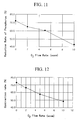
- FIG. 11 is a graph showing a dependency of the reduction rate of phosphorus in the phosphorus-containing insulating film on the flow rate.
- the ordinate of FIG. 11 shows the reduction rate (%) of phosphorus illustrated with linear scales, and the abscissa of FIG. 11 shows the flow rate (sccm) of oxygen (O 2 ) illustrated with linear scales.
- FIG. 12 is a graph showing a dependency of the contraction rate of the phosphorus-containing insulating film on the O 2 flow rate.
- the ordinate of FIG. 12 shows the contraction rate (%) of the phosphorus-containing insulating film illustrated with linear scales, and the abscissa of FIG. 12 shows the O 2 flow rate (sccm) illustrated with linear scales.
- the reason why the reduction rate of phosphorus decreases as the addition amount of oxygen increases and as the contraction rate of the phosphorus-containing insulating film decreases is considered as follows. Specifically, as the addition amount of oxygen increases, the decomposition of the grown film immediately after the film formation is promoted, and phosphorus immediately after the film formation is converted from trivalent phosphorus to pentavalent phosphorus by the addition of oxygen.
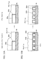
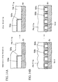
- FIGS. 13, 14 and 15 are photographs of the cross section of the substrate 101 obtained by observing the section of the deposited film with an electron microscope immediately after the film formation and after annealing. These photographs are intended to clarify the difference between the presence and absence of oxygen as the oxidative gas.
- FIGS. 13A, 14A and 15A illustrate a part of the substrate 101 where the doped polysilicon film 52a having a film thickness of about 0.5 ⁇ m, which is deposited on the thermal oxide underlying film 51, is patterned and the thermal oxide film 53a of a film thickness of about 0.1 ⁇ m is formed thereon to form a step difference portion as shown in FIG. 16A.
- FIGS. 13A, 14A and 15A illustrate a part of the substrate 101 where the doped polysilicon film 52a having a film thickness of about 0.5 ⁇ m, which is deposited on the thermal oxide underlying film 51, is patterned and the thermal oxide film 53a of a film thickness of about 0.1 ⁇ m is formed thereon to form a step difference portion as shown in FIG. 16A.
- FIGS. 13A, 14A and 15A illustrate a part of the substrate 101 where the doped polysilicon film 52a having a film thickness of about 0.5 ⁇ m, which is deposited on the thermal oxide underlying film 51, is patterned
- 13B, 14B and 15B illustrate the another part of the substrate 101 where the doped polysilicon film 52a having a film thickness of about 0.4 ⁇ m, which is deposited on the thermal oxide underlying film 51, is patterned to form a plurality of belt-shaped layers 52b disposed at intervals of about 0.35 ⁇ m and the thermal oxide film 53b having a film thickness of about 0.1 ⁇ m is formed thereon, as shown in FIG. 16B.
- the film-forming conditions of the samples used for the investigations shown in FIGS. 13A and 13B were set to be the same as those used for the investigations shown in FIG. 11. Note that O 2 as the oxidative gas was added by the flow rate of 2 sccm.
- the film-forming conditions of the samples used for the investigations shown in FIGS. 14A and 14B were set to be the same as those used for the investigations shown in FIGS. 13A and 13B. Note that O 2 was not added.
- the annealing conditions in FIGS. 14A and 14B were set to be the same as those of the samples used for the investigations of FIGS. 10A and 10B.
- the film-forming conditions of the samples used for the investigations of FIGS. 15A and 15B were set to be the same as those used for the investigations of FIGS. 10A and 10B.
- Ar was used as the carrier gas
- O 2 as the oxidative gas was added at a flow rate of 2 sccm.
- N 2 gas was used as the atmospheric gas
- the substrate temperature was set at 650 °C
- the treatment time was set to five minutes.
- FIGS. 13A to 15A and FIGS. 13B to 15B voids, which were created in its super fine portions (0.12 ⁇ m) immediately after the film formation, were vanished in the film formed by adding oxygen, as shown in FIG. 13B.
- the addition amount of oxygen should be set at a flow rate of 15 sccm or less, more preferably below 10 sccm.
- the annealing temperature is set at 650 °C in the third embodiment, this invention is not limited to this temperature, and the annealing temperature may be a temperature below 650 °C, or preferably below 500 °C.
- HMDSO is used for the silicon-containing compound
- other silicon-containing compounds containing at most one oxygen atom may be used.
- N 2 or Ar gas is used as the carrier gas
- He gas may be also used.
- O 2 gas is used as the oxidative gas, and, as a matter of course, other oxidative gases, for example, CO, CO 2 , NO, N 2 O and NO 2 may be used. Alternatively, the oxidative gas should not be necessarily added.
- the parallel plane type PECVD apparatus is used as the film formation apparatus for embodying the PECVD method.
- the present invention is not limited to this.
- Other PECVD apparatuses such as an ECR (Electron Cyclotron Resonance) type PECVD apparatus can be used.
- the frequency of the RF power for converting the gas into a plasma is not limited to 13.56 MHz, and the RF power with a frequency ranging from 380 kHz to 2.45 GHz may be used.
- the phosphorus-containing insulating film is formed in such a manner that a small amount of oxidative gas is added to the mixed gas obtained by mixing the phosphorus-containing compound containing trivalent phosphorus with the silicon-containing compound containing oxygen at most one atom.
- the insulating film is formed by adding no oxidative gas to that mixed gas.
- the phosphorus-containing insulating film can be formed under the state of oxygen shortage, the phosphorus-containing insulating film with a high concentration of P 2 O 3 can be formed, and the fluidizing temperature can be significantly lowered to 500 °C or less.
- the film-forming rate can be maintained.
- the film-forming rate can be maintained.
- the interlayer insulating film can be flattened, so that the concave portions between the wiring layers can be filled completely.
Landscapes
- Chemical & Material Sciences (AREA)
- Inorganic Chemistry (AREA)
- General Chemical & Material Sciences (AREA)
- Chemical Kinetics & Catalysis (AREA)
- Engineering & Computer Science (AREA)
- Materials Engineering (AREA)
- Mechanical Engineering (AREA)
- Metallurgy (AREA)
- Organic Chemistry (AREA)
- Formation Of Insulating Films (AREA)
- Internal Circuitry In Semiconductor Integrated Circuit Devices (AREA)
Applications Claiming Priority (2)
| Application Number | Priority Date | Filing Date | Title |
|---|---|---|---|
| JP34540498 | 1998-12-04 | ||
| JP34540498A JP3251554B2 (ja) | 1998-12-04 | 1998-12-04 | 成膜方法及び半導体装置の製造方法 |
Publications (2)
| Publication Number | Publication Date |
|---|---|
| EP1006569A2 true EP1006569A2 (de) | 2000-06-07 |
| EP1006569A3 EP1006569A3 (de) | 2001-07-18 |
Family
ID=18376373
Family Applications (1)
| Application Number | Title | Priority Date | Filing Date |
|---|---|---|---|
| EP99114234A Withdrawn EP1006569A3 (de) | 1998-12-04 | 1999-07-27 | Abscheidung eines isolierenden Films |
Country Status (5)
| Country | Link |
|---|---|
| US (1) | US6221755B1 (de) |
| EP (1) | EP1006569A3 (de) |
| JP (1) | JP3251554B2 (de) |
| KR (1) | KR100339820B1 (de) |
| TW (1) | TW413850B (de) |
Cited By (2)
| Publication number | Priority date | Publication date | Assignee | Title |
|---|---|---|---|---|
| DE102004032761A1 (de) * | 2004-07-06 | 2006-01-26 | Infineon Technologies Ag | Verfahren zur Herstellung komplex strukturierter Leitbahnebenen mit Kontaktflächen auf elektronischen Bauelementen |
| EP2953155A1 (de) * | 2014-06-02 | 2015-12-09 | L'air Liquide, Societe Anonyme Pour L'etude Et L'exploitation Des Procedes Georges Claude | Verwendung von Si-O-Si-basierten Molekülen zur Ablagerung einer amorphen Siliciumoxidschicht auf einem Substrat |
Families Citing this family (6)
| Publication number | Priority date | Publication date | Assignee | Title |
|---|---|---|---|---|
| US6458720B1 (en) | 1999-07-23 | 2002-10-01 | Matsushita Electric Industrial Co., Ltd. | Method for forming interlayer dielectric film |
| JP3400770B2 (ja) * | 1999-11-16 | 2003-04-28 | 松下電器産業株式会社 | エッチング方法、半導体装置及びその製造方法 |
| JP4606552B2 (ja) * | 2000-06-27 | 2011-01-05 | 富士通株式会社 | 半導体装置 |
| US20020182342A1 (en) * | 2001-04-13 | 2002-12-05 | Luc Ouellet | Optical quality silica films |
| TW564499B (en) * | 2002-05-20 | 2003-12-01 | Mitsubishi Electric Corp | Method for manufacturing a semiconductor device |
| US7145182B2 (en) * | 2003-09-12 | 2006-12-05 | Avago Technologies General Ip (Singapore) Pte. Ltd. | Integrated emitter devices having beam divergence reducing encapsulation layer |
Family Cites Families (11)
| Publication number | Priority date | Publication date | Assignee | Title |
|---|---|---|---|---|
| JPH0346228A (ja) * | 1989-07-13 | 1991-02-27 | Kojundo Chem Lab Co Ltd | 酸化膜形成法 |
| JPH0719777B2 (ja) * | 1990-08-10 | 1995-03-06 | 株式会社半導体プロセス研究所 | 半導体装置の製造方法 |
| JPH06120207A (ja) * | 1992-10-07 | 1994-04-28 | Sumitomo Metal Ind Ltd | 絶縁膜の形成方法 |
| US5409743A (en) * | 1993-05-14 | 1995-04-25 | International Business Machines Corporation | PECVD process for forming BPSG with low flow temperature |
| JPH0817173B2 (ja) * | 1993-11-10 | 1996-02-21 | キヤノン販売株式会社 | 成膜方法 |
| JP2899600B2 (ja) * | 1994-01-25 | 1999-06-02 | キヤノン販売 株式会社 | 成膜方法 |
| JP3721208B2 (ja) * | 1994-11-08 | 2005-11-30 | 旭電化工業株式会社 | 気相成長によるリン珪酸ガラス膜の形成法 |
| US5895259A (en) * | 1996-05-15 | 1999-04-20 | Advanced Micro Devices, Inc. | Polysilicon diffusion doping method employing a deposited doped oxide layer with a highly uniform thickness |
| JP2983476B2 (ja) * | 1996-10-30 | 1999-11-29 | キヤノン販売株式会社 | 成膜方法及び半導体装置の製造方法 |
| US6013584A (en) * | 1997-02-19 | 2000-01-11 | Applied Materials, Inc. | Methods and apparatus for forming HDP-CVD PSG film used for advanced pre-metal dielectric layer applications |
| JP4050804B2 (ja) * | 1997-04-30 | 2008-02-20 | 株式会社Adeka | リン珪酸ガラス膜の形成法 |
-
1998
- 1998-12-04 JP JP34540498A patent/JP3251554B2/ja not_active Expired - Fee Related
-
1999
- 1999-07-22 US US09/358,399 patent/US6221755B1/en not_active Expired - Fee Related
- 1999-07-23 TW TW088112529A patent/TW413850B/zh not_active IP Right Cessation
- 1999-07-27 EP EP99114234A patent/EP1006569A3/de not_active Withdrawn
- 1999-08-03 KR KR1019990031795A patent/KR100339820B1/ko not_active Expired - Fee Related
Cited By (2)
| Publication number | Priority date | Publication date | Assignee | Title |
|---|---|---|---|---|
| DE102004032761A1 (de) * | 2004-07-06 | 2006-01-26 | Infineon Technologies Ag | Verfahren zur Herstellung komplex strukturierter Leitbahnebenen mit Kontaktflächen auf elektronischen Bauelementen |
| EP2953155A1 (de) * | 2014-06-02 | 2015-12-09 | L'air Liquide, Societe Anonyme Pour L'etude Et L'exploitation Des Procedes Georges Claude | Verwendung von Si-O-Si-basierten Molekülen zur Ablagerung einer amorphen Siliciumoxidschicht auf einem Substrat |
Also Published As
| Publication number | Publication date |
|---|---|
| KR20000047452A (ko) | 2000-07-25 |
| JP2000174013A (ja) | 2000-06-23 |
| KR100339820B1 (ko) | 2002-06-07 |
| US6221755B1 (en) | 2001-04-24 |
| JP3251554B2 (ja) | 2002-01-28 |
| EP1006569A3 (de) | 2001-07-18 |
| TW413850B (en) | 2000-12-01 |
Similar Documents
| Publication | Publication Date | Title |
|---|---|---|
| JP2983476B2 (ja) | 成膜方法及び半導体装置の製造方法 | |
| JP3419745B2 (ja) | 半導体装置及びその製造方法 | |
| US5840631A (en) | Method of manufacturing semiconductor device | |
| US7498273B2 (en) | Formation of high quality dielectric films of silicon dioxide for STI: usage of different siloxane-based precursors for harp II—remote plasma enhanced deposition processes | |
| US7943531B2 (en) | Methods for forming a silicon oxide layer over a substrate | |
| US8481403B1 (en) | Flowable film dielectric gap fill process | |
| US20050136240A1 (en) | Very low dielectric constant plasma-enhanced CVD films | |
| US20050181633A1 (en) | Precursors for depositing silicon-containing films and processes thereof | |
| JP4032044B2 (ja) | 成膜方法、半導体装置の製造方法及び半導体装置 | |
| JP2005294333A (ja) | 成膜方法及び半導体装置 | |
| US6221755B1 (en) | Film formation method and manufacturing method of semiconductor device | |
| Vassiliev et al. | Growth Kinetics and Deposition‐Related Properties of Subatmospheric Pressure Chemical Vapor Deposited Borophosphosilicate Glass Film | |
| US6562735B1 (en) | Control of reaction rate in formation of low k carbon-containing silicon oxide dielectric material using organosilane, unsubstituted silane, and hydrogen peroxide reactants | |
| US6432839B2 (en) | Film forming method and manufacturing method of semiconductor device | |
| EP1128421A2 (de) | Verfahren zur Herstellung einer Zwischenisolationsschicht mit Si, O, C und H für Halbleiterbauelemente | |
| JP4426808B2 (ja) | 成膜方法及び半導体装置の製造方法 | |
| JPH07193129A (ja) | 半導体装置の製造方法 | |
| JPH09293716A (ja) | フッ素含有絶縁膜の形成方法 |
Legal Events
| Date | Code | Title | Description |
|---|---|---|---|
| PUAI | Public reference made under article 153(3) epc to a published international application that has entered the european phase |
Free format text: ORIGINAL CODE: 0009012 |
|
| AK | Designated contracting states |
Kind code of ref document: A2 Designated state(s): DE FR GB NL |
|
| AX | Request for extension of the european patent |
Free format text: AL;LT;LV;MK;RO;SI |
|
| PUAL | Search report despatched |
Free format text: ORIGINAL CODE: 0009013 |
|
| AK | Designated contracting states |
Kind code of ref document: A3 Designated state(s): AT BE CH CY DE DK ES FI FR GB GR IE IT LI LU MC NL PT SE |
|
| AX | Request for extension of the european patent |
Free format text: AL;LT;LV;MK;RO;SI |
|
| 17P | Request for examination filed |
Effective date: 20011010 |
|
| AKX | Designation fees paid |
Free format text: DE FR GB NL |
|
| RBV | Designated contracting states (corrected) |
Designated state(s): DE FR GB NL |
|
| STAA | Information on the status of an ep patent application or granted ep patent |
Free format text: STATUS: THE APPLICATION HAS BEEN WITHDRAWN |
|
| 18W | Application withdrawn |
Effective date: 20030617 |
|
| R18W | Application withdrawn (corrected) |
Effective date: 20030617 |