EP2975554A2 - Oberflächensensor - Google Patents
Oberflächensensor Download PDFInfo
- Publication number
- EP2975554A2 EP2975554A2 EP15183328.2A EP15183328A EP2975554A2 EP 2975554 A2 EP2975554 A2 EP 2975554A2 EP 15183328 A EP15183328 A EP 15183328A EP 2975554 A2 EP2975554 A2 EP 2975554A2
- Authority
- EP
- European Patent Office
- Prior art keywords
- electrodes
- conductive paths
- circuit board
- sensor unit
- smart card
- Prior art date
- Legal status (The legal status is an assumption and is not a legal conclusion. Google has not performed a legal analysis and makes no representation as to the accuracy of the status listed.)
- Ceased
Links
Images




Classifications
-
- G—PHYSICS
- G06—COMPUTING OR CALCULATING; COUNTING
- G06V—IMAGE OR VIDEO RECOGNITION OR UNDERSTANDING
- G06V40/00—Recognition of biometric, human-related or animal-related patterns in image or video data
- G06V40/10—Human or animal bodies, e.g. vehicle occupants or pedestrians; Body parts, e.g. hands
- G06V40/12—Fingerprints or palmprints
- G06V40/13—Sensors therefor
- G06V40/1329—Protecting the fingerprint sensor against damage caused by the finger
-
- G—PHYSICS
- G06—COMPUTING OR CALCULATING; COUNTING
- G06V—IMAGE OR VIDEO RECOGNITION OR UNDERSTANDING
- G06V40/00—Recognition of biometric, human-related or animal-related patterns in image or video data
- G06V40/10—Human or animal bodies, e.g. vehicle occupants or pedestrians; Body parts, e.g. hands
- G06V40/12—Fingerprints or palmprints
- G06V40/13—Sensors therefor
- G06V40/1306—Sensors therefor non-optical, e.g. ultrasonic or capacitive sensing
-
- G—PHYSICS
- G06—COMPUTING OR CALCULATING; COUNTING
- G06K—GRAPHICAL DATA READING; PRESENTATION OF DATA; RECORD CARRIERS; HANDLING RECORD CARRIERS
- G06K19/00—Record carriers for use with machines and with at least a part designed to carry digital markings
- G06K19/06—Record carriers for use with machines and with at least a part designed to carry digital markings characterised by the kind of the digital marking, e.g. shape, nature, code
- G06K19/067—Record carriers with conductive marks, printed circuits or semiconductor circuit elements, e.g. credit or identity cards also with resonating or responding marks without active components
- G06K19/07—Record carriers with conductive marks, printed circuits or semiconductor circuit elements, e.g. credit or identity cards also with resonating or responding marks without active components with integrated circuit chips
- G06K19/077—Constructional details, e.g. mounting of circuits in the carrier
- G06K19/07701—Constructional details, e.g. mounting of circuits in the carrier the record carrier comprising an interface suitable for human interaction
-
- G—PHYSICS
- G06—COMPUTING OR CALCULATING; COUNTING
- G06V—IMAGE OR VIDEO RECOGNITION OR UNDERSTANDING
- G06V40/00—Recognition of biometric, human-related or animal-related patterns in image or video data
- G06V40/10—Human or animal bodies, e.g. vehicle occupants or pedestrians; Body parts, e.g. hands
- G06V40/12—Fingerprints or palmprints
- G06V40/13—Sensors therefor
- G06V40/1312—Sensors therefor direct reading, e.g. contactless acquisition
-
- H—ELECTRICITY
- H10—SEMICONDUCTOR DEVICES; ELECTRIC SOLID-STATE DEVICES NOT OTHERWISE PROVIDED FOR
- H10W—GENERIC PACKAGES, INTERCONNECTIONS, CONNECTORS OR OTHER CONSTRUCTIONAL DETAILS OF DEVICES COVERED BY CLASS H10
- H10W70/00—Package substrates; Interposers; Redistribution layers [RDL]
- H10W70/60—Insulating or insulated package substrates; Interposers; Redistribution layers
- H10W70/62—Insulating or insulated package substrates; Interposers; Redistribution layers characterised by their interconnections
- H10W70/63—Vias, e.g. via plugs
-
- H—ELECTRICITY
- H10—SEMICONDUCTOR DEVICES; ELECTRIC SOLID-STATE DEVICES NOT OTHERWISE PROVIDED FOR
- H10W—GENERIC PACKAGES, INTERCONNECTIONS, CONNECTORS OR OTHER CONSTRUCTIONAL DETAILS OF DEVICES COVERED BY CLASS H10
- H10W90/00—Package configurations
- H10W90/701—Package configurations characterised by the relative positions of pads or connectors relative to package parts
- H10W90/721—Package configurations characterised by the relative positions of pads or connectors relative to package parts of bump connectors
- H10W90/724—Package configurations characterised by the relative positions of pads or connectors relative to package parts of bump connectors between a chip and a stacked insulating package substrate, interposer or RDL
Definitions
- the present invention relates to a sensor for detection of structures and properties of organic tissue or its surface, especially a fingerprint sensor, comprising a chosen number of sensor electrodes at chosen positions for electrical and mechanical coupling to a finger surface and its tissue, having a size comparable to the size of the structures, characteristics, or properties of the finger tissue or surface.
- a fingerprint sensor which may be flush mounted in the same plane as the surface of the product it is mounted into is described in US7251351 , in which a set of first electrodes/sensor elements are positioned on one side of an insulating substrate provided with through-substrate-via conductors.
- the substrate may be made from glass, ceramics or other insulating materials.
- a substrate made from a multilayered or laminate PCB process is described being based on a subtractive PCB process in which, as with the abovementioned US patent, is based on the removal of materials, e.g. by etching, which has relatively low resolution and thus not sufficiently good for the small dimensions and tolerances of fingerprint sensors. If the dimensions such as the layer thickness are not sufficiently accurate they may affect the measurements and reduce the accuracy of the sensor unit.
- the fingerprint sensor is thus manufactured using additive or semi-additive build-up processes to deposit dielectrics and conductors in layers to form a substrate with through going conductive paths, having embedded sensor electrodes for coupling to the finger surface on one side and with the processing unit well protected on the opposite side.
- the substrate may be manufactured using liquid or dry film dielectrics alternated with layers of conductive materials deposited through sputter, spray or other plating technology. Starting with a dielectric layer deposited on a mandrel, for instance glass, the first dielectric layer is ensured a high degree of flatness. Subsequent layers of conductive material and dielectrics are added using photo lithography and corresponding mask sets to define required section features.
- the finished substrate may be post - processed while still attached to the mandrel, or peeled off to reveal the first deposited layer.
- a liquid polymer such as polyimide is used on a flat glass surface thus obtaining an improved accuracy in the dimensions of the sensor unit, especially the thickness and thus the contribution of the substrate structure on the provided measurements.
- An alternative to the above mentioned process is to reverse the layer processing sequence. Instead of first depositing the top finger interface layer onto a glass plate, one or multiple layers are deposited onto a PCB type core.
- the core may be pre fabricated with a rear side processing unit interface and internal layers for signal redistribution and shielding.
- the front side of the PCB type core may then be post processed using the build-up processes described above to produce the small, high tolerance, features required for the fingerprint sensor design.
- the last layer to be deposited will in this process constitute the finger interface.
- This processing alternative is often utilized to manufacture IC substrates or Flip Chip substrates, and is often referred to as Micro PCB.
- the term "detection of voltage or current” will be understood by a person skilled in the art as a method for detection and collection of information about the related capacitance, impedance, electromagnetic field, fingerprint or other biometric, physical, physiological, thermal or optical or characteristics or properties of the tissue or its surface positioned over the electrodes of the sensor.
- the term coupling is understood as including both direct electrical contact between two parts as well as capacitive or inductive coupling of two parts separated physically by a dielectric material.
- Figure 1 illustrates the cross section of the preferred embodiment of the fingerprint sensor 21 according to the invention.
- the sensor unit is constituted by a flexible unit 40 including a dielectric, possibly organic, substrate 8 with embedded conductive sections 1,2,3,4.
- First electrodes 1 are connected to first conductive paths 4, created by sequentially depositing layers of conductive and dielectric materials forming unbroken conductive paths of conductive sections from the first electrodes, through the substrate 8 and redistributed to coupling points 31 for connecting to the processing unit interfaces 7 on the reverse side.
- This structure is preferably built in a build-up process as mentioned above and may include several additional steps for introducing additional layers, e.g. if the required positions of the coupling points to the processing unit is different from the positions of the electrodes.
- the finger interface, coupling area, of the first electrodes 1 are chosen so that they are smaller than structures in a typical finger surface 10, enabling the capability to distinguishing between valleys and ridges in the surface which typically have a pitch of approximately 150- 600 ⁇ m.
- a typical area of the first electrodes may therefore be approximately 2000-20000 ⁇ m 2 , electrically insulated from adjacent electrodes by the substrate dielectric in a thickness of 1-30 ⁇ m.
- Other versions may be contemplated varying electrode size, shape and pitch. In a realized embodiment the electrode pitch is 67.5 ⁇ m, in a rectangular shape with an area of 6500 ⁇ m 2 .
- the conductive paths 4 may vary greatly in size and shape depending on routing and / or process constraints as well as signal integrity requirements.
- L/S trace widths and thicknesses
- layer to layer interconnecting conductive paths with cross sectional areas of 10-2000 ⁇ m 2 .
- a current embodiment is realized with L/S of 15/15 ⁇ m and layer to layer interconnects of 700 ⁇ m 2
- the preferred embodiment of the invention involves galvanic isolation between the finger surface and the sensor electrodes and thus the sensor electrodes are embedded in the substrate below the finger interface surface, the substrate dielectric 8 providing the required dielectric medium between the finger surface and first electrodes.
- a surface coating layer 9 is added for improved mechanical and chemical protection, controlled friction, improved image quality, enhanced cosmetics or other purposes.
- the performance coating may be made from a carbon based materials such as Diamond Like carbon (DLC) or amorphous diamond, as described in EP0779497 and US5963679 .
- the thickness of the substrate dielectric and performance coating layers may be chosen to provide suitable detection conditions, for example in the range of 500nm or more. Exposed electrodes without dielectrics providing direct electrical contact with the finger may be implemented for improved detection conditions, like increased signal levels.
- the fingerprint sensor substrate is in a per se known way provided with electrical signal interfaces 7 for connecting the signal processing unit 13 to the conductive paths.
- electrical signal interfaces 7 may be manufactured using well known technology for under - bump metallization (UBM) and provide a base for solder or glue based interconnection solutions to the processing unit.
- UBM under - bump metallization
- external IO connections 15 are provided.
- the substrate is also provided with a second electrode 2 connected to a second conductive path 5 implemented in a similar manner as the first electrode and first conductive path but having larger electrode dimensions so as to be significantly larger than the features in the finger surface.
- the processing unit is adapted to detect the voltage at or the current flow in each of a multitude of first electrodes 1 provided by the first and second electrodes as the processing unit also applies a static or varying voltage between the first and second electrodes and detects the voltage and current in a per se known way, e.g.
- the substrate is also provided with a third electrode 3 connected to a third conductive path 6 implemented in a similar manner as the first electrode and first conductive path.
- the third electrode may vary in size from smaller than, to significantly larger than the surface feature size of the finger.
- the third electrode may replicate the functionality of the first or second electrodes or be independently electrically exited, modulated, electrically left floating, or connected to ground as discussed in US7606398 .
- the third electrode may also be implemented in such a way that a capacitive coupling to individual 1 st electrodes may be utilized in a calibration or circuit test routine as described in US 7251351B2 .
- Other alternatives may also be contemplated, e.g.
- the fingerprint sensor is designed as a swipe sensor where the surface to be measured is expected to traverse the electrodes in the swipe direction 11.
- Figure 2 illustrates the layout of a stripe shaped fingerprint sensor 21 constituted by an essentially linear array of sensor electrodes 12 wherein each first electrode 1 is related to one first conductive path 4. Spanning the sensor array 12 are two stimulation or drive electrodes 2, related to before mentioned second conductive paths, thus ensuring a uniform voltage distribution across the finger, and the variation in the detected signal from the sensor array being mainly caused by variations in the structure of the finger in close vicinity to the array.
- the layout also includes two third electrodes 3, in this instance used for a (digital and analog) ground connection, thus also providing ESD protection.
- These electrodes may also be related to before mentioned third conductive paths through the substrate.
- the embedded depth of these electrodes may be varied similarly to the first and second electrodes to increase the probability of ESD events to discharge to ground.
- Other solutions for providing ESD protection may be realized by implementation of diode structures connected to the conductive paths of the substrate.
- Alternatively a discrete component such as an ESD protection diode may be connected between the drive electrode and ground, internally embedded in the substrate or externally connected for instance by flip-chip assembly.
- the sensor array may be constituted by one or multiple linear arrays of electrodes, possibly shifted across the swipe direction providing a staggered structure and improving the resolution in the measurements.
- Multiple sensor arrays may also allow for reconstructing a fingerprint image by stitching as described in US6289114 or for measuring the movement of the finger over the sensor as described in US7054471 .
- the second, third, or both electrodes may be provided with interfaces to external IO connections 15 shown in Figure 1 for implementation outside the substrate, with the advantage of reducing the substrate material area as discussed in US 6,628,812 and US 6,683,971 .
- Additional electrodes and circuitry may be embedded in the sensor 21, for example for measuring the relative movement of the finger across the surface, as described in US7251351 and US7110577 , or for navigation or driving a pointer on a screen, as described in US7129926 and US7308121 or for measuring other biometric properties of the finger, like aliveness detection.
- an additional internal layer of conductive sections 14 is included for shielding purposes.
- the shield layer is positioned between the electrodes and any conductive sections used for lateral signal redistribution to the processing unit interfaces. Connecting all or sections of this shield layer to ground will protect the processing unit interfaces and signal redistribution sections from electromagnetic interference or inductive or capacitive electrical coupling from the electrodes and finger surface, and vice versa.
- one or more additional internal layers 16 of conductive sections may be included to facilitate various embedded features.
- An additional layer may be included to facilitate improved signal redistribution with additional degrees of freedom to route conductive paths 17.
- One or more additional internal layers of conductive sections may be included to facilitate various embedded components 18.
- a discrete component may be placed on the last deposited layer, connection terminal(s) up, fixed with glue or by other means before the next dielectric layer is deposited.
- the subsequent conductive section layer deposition is prepared with a mask including openings at the required connection positions of the discrete component.
- the conductive material deposition process will fuse to the appropriate discrete component terminals and connect to the appropriate conductive paths.
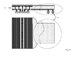
- the alternative embodiment in Figure 4 also illustrates how organic or printable electronic circuits 19 may be implemented.
- the patternable dielectric layer 16 may be used as a base medium for such a deposition process.
- These special circuits are connected to underlying conductive sections directly through their deposition processes, or by fusing to the subsequent conductive layers by its deposition processes.
- a gas filled volume between two conductive sections may be used as a spark gap 20 to provide a high voltage discharge path, and to dissipate electrical charge to ground. ESD protection may hence be improved when incorporated into the conductive paths between electrodes and the processing unit.
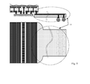
- FIG. 5 is a special case of previously described embedded discrete components 18 of Figure 4 .
- the whole processing unit 13 is embedded in the dielectric, as opposed to flip chip mounted as depicted in Figure 1 .
- a curable polymer resin 22, for example epoxy is used to improve mechanical robustness of the sensor.
- the underfill resin is used to encapsulate electrical interfaces and the processing unit, hence protecting them from the elements such as moisture and dirt, while also adding stiffness to the sensor.
- a sheet with multiple sensors can be underfilled and coated before cutting into individual sensors.
- the finished product is a fingerprint device, encapsulated and packaged with a BGA type ball interface 15.
- a similar result may be achieved using plastic molding processes as opposed to curable resins.
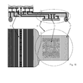
- an additional second dielectric material 23 is laminated onto the build-up substrate to improve stiffness and mechanical robustness of the sensor.
- This material may be a layer of liquid or dry film soldermask where the conductive sections are formed with the same process used to form the conductive sections of the build-up substrate.
- the stiffening layer may be of a printed circuit board type material with preformed via's, interfaced and electrically connected to the buidl-up substrate conductive sections.
- a flexible ribbon cable 24 is integrated in the build-up substrate for external IO connections. This may simplify integration into various applications with the option to increase the distance between the finger interface and host system electronics.
- the ribbon cable may for instance be threaded through a slot in the application enclosure.
- a separate flexible ribbon cable 25 is connected to the external IO connection interface of the build-up substrate yielding advantages similar to what is described for the embodiment in Figure 8 .
- the high resolution build-up substrate 8 is laminated or otherwise fixed with electrical connections to a standard PCB or flexible printed circuit 26 constituting an interposer between the build-up sensor substrate and the signal processing unit 13.
- This may provide advantages in fixturing, interconnecting, and assembling while utilizing a lower cost material for circuitry requiring a larger area.
- the signal processing unit and external IO connections 27 may be located on either side of the interposer.
- the high resolution build-up substrate 8 is laminated or otherwise fixed with electrical connections to a standard PCB or flexible printed circuit 28 constituting a motherboard for an embedded fingerprint module.
- additional electronic circuitry such as integrated circuits, displays, LED's, buttons 29, and external electrical interfaces 30 can be integrated into the fingerprint module.
- the additional electronic circuitry may be located on either side of the motherboard.
- the high resolution build-up substrate 8 is utilized not only as a sensor substrate, but is also implemented as a carrier and interconnect device for a full biometric system.
- 1 st , 2 nd and 3 rd electrode signals are redistributed (not shown) to the signal processing unit 13 located either directly below the finger interface or shifted in any lateral direction.
- Additional integrated circuits such as micro controllers 32 and other electrical components 33 such as capacitors, resistors, buttons, displays and antennas may be integrated either by Flip Chip, wire bonding, conductive glue or other.
- External IO connections 15 may be integrated as exposed conductive pads, headers, and connectors or other.
- the finger interface section may be supported mechanically by a laminated stiffener plate 34 of suitable thickness and material.
- the complete biometric assembly may be mounted inside a suitable enclosure, or molded, alternatively laminated, inside for example an id or financial transaction card.
- the flexible unit 40 with the fingerprint sensor 21 is mounted on a second dielectric material 23 as in figure 7 .
- This second dielectric unit 23 constitutes a circuit board including a bonding interface 41 to connect with the coupling points 31 on the back side of the fingerprint sensor 21 as well as conductor leads through the second dielectric unit to a solder surface 42 on the opposite side on which processors 13 may be placed, thus being connected to the fingerprint sensor 21.
- This solution is especially suitable for mounting in smart cards having an opening or recess adapted to receive the fingerprint sensor unit.
- the sensor unit may then be fastened in the recess or hole using lamination processes or adhesives and sealed to constitute an integral part of the smart card.
- Smart cards are often made in a layered structure having at least three layers where the a middle layer includes conductor leads making it possible to connect to other circuitry in the card.
- An example showing this type of connection is shown in US6881605 .
- the fingerprint sensor is to be positioned in a recess or hole in the card contact points 43 in a position suitable for connecting to the conductive card layer are provided at a suitable position matching the thickness of the outer layers covering the electrical conductors in the card.
- Figure 14 illustrates the fingerprint sensor 21 positioned in a smart card 47 also comprising electrical conductors 44 as well as a microchip 45 and an antenna 46, e.g. for RFID or near field communication.
- electrical conductors 44 are embedded in an intermediate layer inside the smart card while the connector interface of the microchip 45 and fingerprint sensor 21 extend to the card surface.
- the invention refers especially to the realization of fingerprint sensors with sensor electrodes and associated conductive paths embedded in a dielectric substrate.
- the invention relates to a sensor unit for measuring structures and properties by the surface of an object of organic tissue, especially a fingerprint sensor.
- the sensor unit comprising
- the invention primarily relates to a sensor for detection of properties and structures of an organic tissue and its surface, especially a fingerprint sensor, the sensor surface being part of a flexible unit suitable to be included in credit card etc.
- the flexibility may thus preferably be according to the ISO standard for credit cards ISO-IEC 7810.
- the flexibility of the substrate layers without processors and other components may be larger, e.g. with a bend radius down to 1mm. It comprises a chosen number of first electrodes or sensor elements at chosen positions for coupling to a surface to be measured.
- the size of the first electrodes and preferably the distances between them should be less or comparable to the size of the properties or structures in the tissue or its surface so as to be able to distinguish between different types of features such as ridges and valleys in a fingerprint.
- a processing unit may be included having electronic circuitry for detection of voltage at or the current flow in the electrodes, thereby providing for detection and collection of information of related capacitance, impedance, electromagnetic field, fingerprint, structure, tissue aliveness or other biometric, physical, physiological, thermal or optical characteristics or properties of the tissue or its surface.
- This circuitry is connected to said first electrodes for providing detection of said characteristics, properties or structures, the processing unit being mounted on one side of a substrate, and the first electrodes being positioned on internally embedded layers of said substrate.
- the substrate thus includes through going first conductive paths between said sensor electrode and said measurement circuitry, wherein the substrate is made from a flexible single or multi layer dielectric polymer material such as polyimide and said first conductive paths are constituted by through going substrate sections of a chosen size and material.
- the substrate preferably is made from flexible materials and also includes at least one second electrode with a size substantially larger than the structures of the surface to be measured.
- the second electrode may be grounded or connected to said processing unit, with a second conductive path also being constituted by thru going conductive sections of the substrate, and the processing unit is adapted to detect the voltage or current at the first and second electrodes.
- a varying voltage may be applied by the processing unit or an external oscillator between the second electrode and the first electrodes, the processing unit measuring or calculating the impedance between the first electrodes and the second electrode.
- the substrate may also includes at least one third electrode, providing an electrode being coupled to said surface and connected to said processing unit, with a third conductive path also being constituted by thru going conductive leads of the substrate.
- the third electrode may be grounded or the processing unit may be adapted to detect the voltage or current at the third electrode.
- the first, second and third electrodes may be embedded in the same plane or at varying depth, relative to the surface to be measured or completely exposed to the said surface, yielding individual dielectric coupling characteristics for said surface structure measurements.
- the first layer may include areas with reduced thickness or openings over at least some of the electrodes thus also providing means for adjusting the capacitance between the finger and electrode or providing galvanic contact between the electrodes and the finger/object to be measured.
- an outer protective layer made from a carbon based material, e.g. amorphous diamond, covering the measurement surface interface of the surface sensor.
- the substrate may also include at least one external interface to an external electrode outside the substrate being substantially larger than the structures of the surface, providing an external electrode being coupled to said surface to be measured, and connected to said processing unit.
- the third layer of the sensor unit may also include at least one embedded patternable sub-layer for signal redistribution purposes of said first, second or third conductive paths at predetermined positions of connection point for coupling to the processing unit.
- the sub-layer may also include embedded active and passive electronic devices, where at least one electronic devise is implemented between at least two conductive sections of said first, second or third conductive paths.
- the processing unit with measurement circuitry connected to at least two conductive sections of said first, second or third conductive paths, may also be embedded into the substrate structure.
- the substrate may also include at least one embedded organic electronics layer where at least one electronic device is implemented between at least two conductive sections of said first, second or third conductive paths, and or at least one embedded patternable dielectric layer where at lease one void is created to form a spark gap between at least two conductive sections of said first, second or third conductive paths.
- the coupling means provided for coupling to a signal processing unit may be connected to conductors on a flexible foil, PCB or printed circuit, where the conductors provide a connection between the coupling means and a corresponding interface on a signal processing unit positioned in a position laterally separated from the coupling means.
- the processing unit may be positioned in a different position than the sensor surface, either on the same side of the foil, PCB or printed circuit or on the opposite side.
- the printed circuit or PCB may also comprise other circuitry or interfaces to external equipment.
- the sensor unit according to the invention is preferably produced using a method including the steps of:
- the method may also include a step of applying an electrically conductive material on the second ends of the conductive sections for providing connecting means.
- the surface of the sensor may be treated in several ways depending on the use and operating conditions.
- the substrate may be altered for optical properties by patterning and imaging polyimide structure for appearance, reflection etc, or for obtaining surface characteristics such as hydrophobicity, friction, resistance to wear etc.
- the substrate may also be altered to accommodate an embedded processing unit, or coated with a hardened curing resin on the processing unit side to form an encapsulated device with a ball grid array type external IO interface. In order to make it more durable it may also be laminated onto another surface for added rigidity and interconnection purposes such as a printed circuit board.
- the substrate may be lamination onto a curved surface, e.g. so as to obtain a solution similar to the swipe sensor described in US 6785407 .
- a flexible substrate may be obtained which may function as a part of a flexible ribbon cable for interconnection purposes, or be laminated onto a flexible flat cable for interconnection purposes. It may also laminated or otherwise electrically connected to a PCB or flexible circuit, constituting an interposer between said substrate and said processing unit for additional degrees of freedom in layout of assembly and interconnections or a motherboard for an embedded fingerprint module, providing an interface between said sensor substrate and processing unit, while allowing for additional electronic circuitry and components to be
Landscapes
- Engineering & Computer Science (AREA)
- Physics & Mathematics (AREA)
- General Physics & Mathematics (AREA)
- Theoretical Computer Science (AREA)
- Human Computer Interaction (AREA)
- Multimedia (AREA)
- Computer Hardware Design (AREA)
- Microelectronics & Electronic Packaging (AREA)
- Image Input (AREA)
- Measurement Of Length, Angles, Or The Like Using Electric Or Magnetic Means (AREA)
- Measurement Of The Respiration, Hearing Ability, Form, And Blood Characteristics Of Living Organisms (AREA)
Applications Claiming Priority (3)
| Application Number | Priority Date | Filing Date | Title |
|---|---|---|---|
| US29063009P | 2009-12-29 | 2009-12-29 | |
| NO20093601A NO20093601A1 (no) | 2009-12-29 | 2009-12-29 | Overflatesensor |
| EP10798350A EP2519913A1 (de) | 2009-12-29 | 2010-12-28 | Oberflächensensor |
Related Parent Applications (1)
| Application Number | Title | Priority Date | Filing Date |
|---|---|---|---|
| EP10798350A Division EP2519913A1 (de) | 2009-12-29 | 2010-12-28 | Oberflächensensor |
Publications (2)
| Publication Number | Publication Date |
|---|---|
| EP2975554A2 true EP2975554A2 (de) | 2016-01-20 |
| EP2975554A3 EP2975554A3 (de) | 2016-03-23 |
Family
ID=44246927
Family Applications (2)
| Application Number | Title | Priority Date | Filing Date |
|---|---|---|---|
| EP15183328.2A Ceased EP2975554A3 (de) | 2009-12-29 | 2010-12-28 | Oberflächensensor |
| EP10798350A Ceased EP2519913A1 (de) | 2009-12-29 | 2010-12-28 | Oberflächensensor |
Family Applications After (1)
| Application Number | Title | Priority Date | Filing Date |
|---|---|---|---|
| EP10798350A Ceased EP2519913A1 (de) | 2009-12-29 | 2010-12-28 | Oberflächensensor |
Country Status (7)
| Country | Link |
|---|---|
| US (4) | US9122901B2 (de) |
| EP (2) | EP2975554A3 (de) |
| JP (1) | JP5753857B2 (de) |
| CN (1) | CN102782700A (de) |
| NO (1) | NO20093601A1 (de) |
| TW (1) | TWI511052B (de) |
| WO (1) | WO2011080262A1 (de) |
Families Citing this family (123)
| Publication number | Priority date | Publication date | Assignee | Title |
|---|---|---|---|---|
| JP3441539B2 (ja) | 1994-10-26 | 2003-09-02 | 日本エレクトロプレイテイング・エンジニヤース株式会社 | 無電解金めっき液によるめっき方法及びその装置 |
| US8022554B2 (en) | 2006-06-15 | 2011-09-20 | Sitime Corporation | Stacked die package for MEMS resonator system |
| NO20093601A1 (no) | 2009-12-29 | 2011-06-30 | Idex Asa | Overflatesensor |
| PT3581105T (pt) | 2010-05-08 | 2022-10-19 | Univ California | Dispositivo para detecção precoce de úlceras por rastreio da humidade subepidermal |
| US10043052B2 (en) * | 2011-10-27 | 2018-08-07 | Synaptics Incorporated | Electronic device packages and methods |
| US9695036B1 (en) * | 2012-02-02 | 2017-07-04 | Sitime Corporation | Temperature insensitive resonant elements and oscillators and methods of designing and manufacturing same |
| US9740343B2 (en) | 2012-04-13 | 2017-08-22 | Apple Inc. | Capacitive sensing array modulation |
| GB201208680D0 (en) | 2012-05-17 | 2012-06-27 | Origold As | Method of manufacturing an electronic card |
| US9581628B2 (en) * | 2012-05-04 | 2017-02-28 | Apple Inc. | Electronic device including device ground coupled finger coupling electrode and array shielding electrode and related methods |
| US9030440B2 (en) | 2012-05-18 | 2015-05-12 | Apple Inc. | Capacitive sensor packaging |
| TWI491059B (zh) * | 2012-10-04 | 2015-07-01 | 力智電子股份有限公司 | 接近感測器及其電路佈局方法 |
| KR102204765B1 (ko) | 2012-10-14 | 2021-01-19 | 시냅틱스 인코포레이티드 | 지문 센서와 버튼 조합들 및 그 제조 방법들 |
| US9651513B2 (en) | 2012-10-14 | 2017-05-16 | Synaptics Incorporated | Fingerprint sensor and button combinations and methods of making same |
| NO20131423A1 (no) | 2013-02-22 | 2014-08-25 | Idex Asa | Integrert fingeravtrykksensor |
| US9888283B2 (en) | 2013-03-13 | 2018-02-06 | Nagrastar Llc | Systems and methods for performing transport I/O |
| USD758372S1 (en) * | 2013-03-13 | 2016-06-07 | Nagrastar Llc | Smart card interface |
| NL2012891B1 (en) | 2013-06-05 | 2016-06-21 | Apple Inc | Biometric sensor chip having distributed sensor and control circuitry. |
| US9883822B2 (en) | 2013-06-05 | 2018-02-06 | Apple Inc. | Biometric sensor chip having distributed sensor and control circuitry |
| US20150335288A1 (en) | 2013-06-06 | 2015-11-26 | Tricord Holdings, Llc | Modular physiologic monitoring systems, kits, and methods |
| SG11201509901VA (en) | 2013-06-06 | 2016-01-28 | Tricord Holdings L L C | Modular physiologic monitoring systems, kits, and methods |
| NO336318B1 (no) | 2013-07-12 | 2015-08-03 | Idex Asa | Overflatesensor |
| US9984270B2 (en) | 2013-08-05 | 2018-05-29 | Apple Inc. | Fingerprint sensor in an electronic device |
| KR20150018350A (ko) * | 2013-08-08 | 2015-02-23 | 삼성전자주식회사 | 지문인식장치와 그 제조방법 및 전자기기 |
| JP6654566B2 (ja) * | 2013-08-23 | 2020-02-26 | フィンガープリント カーズ アーベー | 指紋検知システムの接続パッド |
| US9460332B1 (en) | 2013-09-09 | 2016-10-04 | Apple Inc. | Capacitive fingerprint sensor including an electrostatic lens |
| US10296773B2 (en) | 2013-09-09 | 2019-05-21 | Apple Inc. | Capacitive sensing array having electrical isolation |
| US9697409B2 (en) | 2013-09-10 | 2017-07-04 | Apple Inc. | Biometric sensor stack structure |
| EP3072083B1 (de) | 2013-11-22 | 2018-07-18 | Shenzhen Goodix Technology Co., Ltd. | Sicherer menschlicher fingerabdrucksensor |
| EP3075085B1 (de) | 2013-11-27 | 2020-01-08 | Shenzhen Goodix Technology Co., Ltd. | Tragbare kommunikationsvorrichtungen zur gesicherten transaktion und kommunikation |
| US10128907B2 (en) * | 2014-01-09 | 2018-11-13 | Shenzhen GOODIX Technology Co., Ltd. | Fingerprint sensor module-based device-to-device communication |
| CN103793691A (zh) * | 2014-01-28 | 2014-05-14 | 深圳市汇顶科技股份有限公司 | 指纹识别装置及具有其的移动终端 |
| TWI493187B (zh) * | 2014-02-17 | 2015-07-21 | 茂丞科技股份有限公司 | 藉由信號外延結構形成之具有平坦接觸面之生物感測器及其製造方法 |
| US10095906B2 (en) | 2014-02-21 | 2018-10-09 | Idex Asa | Sensor employing overlapping grid lines and conductive probes for extending a sensing surface from the grid lines |
| EP3640842B1 (de) * | 2014-03-12 | 2025-02-12 | Idex Biometrics Asa | Fingerabdruckdetektionsvorrichtung |
| WO2015143011A1 (en) | 2014-03-19 | 2015-09-24 | Bidirectional Display Inc. | Image sensor panel and method for capturing graphical information using same |
| US9122349B1 (en) | 2014-03-19 | 2015-09-01 | Bidirectional Display Inc. | Image sensor panel and method for capturing graphical information using same |
| US9489559B2 (en) | 2014-05-28 | 2016-11-08 | Fingerprint Cards Ab | Electronic device with fingerprint sensing system and conducting housing |
| TWI567886B (zh) * | 2014-05-28 | 2017-01-21 | 南茂科技股份有限公司 | 晶片封裝結構以及晶片封裝結構的製作方法 |
| CN107040621A (zh) * | 2014-06-16 | 2017-08-11 | 深圳市汇顶科技股份有限公司 | 一种移动终端 |
| CN104051366B (zh) * | 2014-07-01 | 2017-06-20 | 苏州晶方半导体科技股份有限公司 | 指纹识别芯片封装结构和封装方法 |
| US9886613B2 (en) | 2014-07-07 | 2018-02-06 | Shenzhen GOODIX Technology Co., Ltd. | Integration of touch screen and fingerprint sensor assembly |
| US9558390B2 (en) * | 2014-07-25 | 2017-01-31 | Qualcomm Incorporated | High-resolution electric field sensor in cover glass |
| TWM493712U (zh) * | 2014-08-01 | 2015-01-11 | Superc Touch Corp | 具有遮罩功能的感應電極之生物辨識裝置 |
| TWI640767B (zh) * | 2014-08-13 | 2018-11-11 | 佳能企業股份有限公司 | 電子傳輸模組及電子裝置 |
| KR102356453B1 (ko) | 2014-08-29 | 2022-01-27 | 삼성전자주식회사 | 지문 인식 센서 및 이를 포함하는 지문 인식 시스템 |
| US9779280B2 (en) | 2014-12-24 | 2017-10-03 | Idex Asa | Fingerprint sensor employing an integrated noise rejection structure |
| AU2016205816B2 (en) * | 2015-01-08 | 2020-07-16 | Medasense Biometrics Ltd. | An electrode array for physiological monitoring and device including or utilizing same |
| CN104657707B (zh) * | 2015-01-30 | 2018-03-20 | 业成光电(深圳)有限公司 | 指纹识别装置及其制作方法 |
| KR102280155B1 (ko) * | 2015-02-04 | 2021-07-22 | 엘지디스플레이 주식회사 | 센서 스크린 및 그를 구비한 표시장치 |
| KR102339546B1 (ko) * | 2015-02-06 | 2021-12-16 | 엘지디스플레이 주식회사 | 센서 스크린 및 그를 구비한 표시장치 |
| KR102097179B1 (ko) * | 2015-04-07 | 2020-04-03 | 앰코테크놀로지코리아(주) | 지문센서 패키지 및 그 제조 방법 |
| CN106056033B (zh) * | 2015-04-14 | 2019-07-05 | 李美燕 | 复合基板感测装置及其制造方法 |
| US10182740B2 (en) | 2015-04-24 | 2019-01-22 | Bruin Biometrics, Llc | Apparatus and methods for determining damaged tissue using sub-epidermal moisture measurements |
| USD864968S1 (en) | 2015-04-30 | 2019-10-29 | Echostar Technologies L.L.C. | Smart card interface |
| KR101942141B1 (ko) | 2015-05-12 | 2019-01-24 | 앰코테크놀로지코리아(주) | 지문센서 패키지 |
| USD776664S1 (en) * | 2015-05-20 | 2017-01-17 | Chaya Coleena Hendrick | Smart card |
| TWI553563B (zh) * | 2015-05-25 | 2016-10-11 | 義隆電子股份有限公司 | 指紋辨識裝置 |
| KR101670894B1 (ko) | 2015-05-27 | 2016-10-31 | (주)파트론 | 반도체 패키지의 제조 방법 |
| CN105447442B (zh) | 2015-06-10 | 2017-08-04 | 比亚迪股份有限公司 | 调整指纹检测芯片激励电压的方法和装置 |
| TWI537837B (zh) * | 2015-06-11 | 2016-06-11 | 南茂科技股份有限公司 | 指紋辨識晶片封裝結構及其製作方法 |
| EP3657388B1 (de) | 2015-06-23 | 2025-08-06 | Idex Biometrics Asa | Doppelseitiger fingerabdrucksensor |
| CN106356348A (zh) * | 2015-07-24 | 2017-01-25 | 晨星半导体股份有限公司 | 电容式传感器结构、具电容式传感器的电路板结构以及电容式传感器的封装结构 |
| US9704012B2 (en) * | 2015-09-10 | 2017-07-11 | Cypress Semiconductor Corporation | Fingerprint sensor pattern |
| US10955977B2 (en) | 2015-11-03 | 2021-03-23 | Microsoft Technology Licensing, Llc | Extender object for multi-modal sensing |
| US10649572B2 (en) | 2015-11-03 | 2020-05-12 | Microsoft Technology Licensing, Llc | Multi-modal sensing surface |
| US10338753B2 (en) | 2015-11-03 | 2019-07-02 | Microsoft Technology Licensing, Llc | Flexible multi-layer sensing surface |
| US9740908B2 (en) * | 2015-11-09 | 2017-08-22 | Contek Life Science Co., Ltd. | Capacitive fingerprint sensor and package method thereof |
| US9898645B2 (en) | 2015-11-17 | 2018-02-20 | Taiwan Semiconductor Manufacturing Company, Ltd. | Fingerprint sensor device and method |
| TWI597670B (zh) * | 2016-01-06 | 2017-09-01 | 晨星半導體股份有限公司 | 指紋辨識電極結構 |
| US9792516B2 (en) * | 2016-01-26 | 2017-10-17 | Next Biometrics Group Asa | Flexible card with fingerprint sensor |
| KR102592972B1 (ko) * | 2016-02-12 | 2023-10-24 | 삼성전자주식회사 | 센싱 모듈 기판 및 이를 포함하는 센싱 모듈 |
| US9914066B2 (en) | 2016-03-07 | 2018-03-13 | Microsoft Technology Licensing, Llc | Electromagnetically coupled building blocks |
| US9773153B1 (en) * | 2016-03-24 | 2017-09-26 | Fingerprint Cards Ab | Fingerprint sensor module |
| SE1650769A1 (sv) * | 2016-06-01 | 2017-10-24 | Fingerprint Cards Ab | Fingerprint sensing device and method for manufacturing a fingerprint sensing device |
| US10426672B2 (en) * | 2016-08-26 | 2019-10-01 | Vener8 Technologies | Moisture detection and notification system |
| CN107844732A (zh) * | 2016-09-18 | 2018-03-27 | 敦泰电子有限公司 | 一种指纹感测器、指纹感测模组和电子设备 |
| US10274449B2 (en) * | 2016-10-17 | 2019-04-30 | Robert Bosch Gmbh | Capacitive moisture sensor system for a surveillance camera |
| US10102412B2 (en) | 2016-11-17 | 2018-10-16 | Fingerprint Cards Ab | Fingerprint sensing with different capacitive configurations |
| US9922231B1 (en) * | 2016-11-17 | 2018-03-20 | Fingerprint Cards Ab | Fingerprint sensing with voltage pattern configurations |
| EP3550297A4 (de) * | 2016-12-02 | 2019-12-18 | Sony Semiconductor Solutions Corporation | Halbleiterbauelement und potenzialmessvorrichtung |
| US11610429B2 (en) | 2016-12-15 | 2023-03-21 | Fingerprint Cards Anacatum Ip Ab | Fingerprint sensing module and method for manufacturing the fingerprint sensing module |
| US10395164B2 (en) | 2016-12-15 | 2019-08-27 | Fingerprint Cards Ab | Fingerprint sensing module and method for manufacturing the fingerprint sensing module |
| US11023702B2 (en) | 2016-12-15 | 2021-06-01 | Fingerprint Cards Ab | Fingerprint sensing module and method for manufacturing the fingerprint sensing module |
| CN118177725A (zh) | 2017-02-03 | 2024-06-14 | 布鲁恩医疗创新有限责任公司 | 糖尿病足溃疡易感性的测量 |
| CN109890272B (zh) | 2017-02-03 | 2022-05-17 | 布鲁恩生物有限责任公司 | 组织存活力的测量 |
| JP6900477B2 (ja) | 2017-02-03 | 2021-07-07 | ブルーイン、バイオメトリクス、リミテッド、ライアビリティー、カンパニーBruin Biometrics, Llc | コンパートメント症候群を評価するための装置、およびコンパートメント症候群を検出するためのコンピュータ可読媒体 |
| KR101989457B1 (ko) * | 2017-02-28 | 2019-06-14 | 동우 화인켐 주식회사 | 고성능 터치 센서 및 그 제조방법 |
| US10282651B2 (en) | 2017-03-23 | 2019-05-07 | Idex Asa | Sensor array system selectively configurable as a fingerprint sensor or data entry device |
| US11250307B2 (en) | 2017-03-23 | 2022-02-15 | Idex Biometrics Asa | Secure, remote biometric enrollment |
| TWI634527B (zh) * | 2017-05-23 | 2018-09-01 | 財團法人工業技術研究院 | 感測系統 |
| FR3069081B1 (fr) | 2017-07-17 | 2021-08-20 | Safran Identity & Security | Carte electronique comprenant un capteur d'empreinte et procede de fabrication d'une telle carte |
| TWI633480B (zh) * | 2017-08-07 | 2018-08-21 | 致伸科技股份有限公司 | 指紋辨識觸控屏 |
| TWI705384B (zh) | 2017-09-19 | 2020-09-21 | 挪威商藝達思公司 | 適合集成於電子裝置的雙面感測器模組 |
| TWI626599B (zh) * | 2017-09-26 | 2018-06-11 | 速博思股份有限公司 | 小曲率半徑指紋偵測器結構 |
| KR20240159026A (ko) | 2017-11-16 | 2024-11-05 | 브루인 바이오메트릭스, 엘엘씨 | 복수의 케어 환경에 걸쳐 케어의 연속성 제공 |
| WO2019116233A1 (en) | 2017-12-12 | 2019-06-20 | Idex Asa | Power source for biometric enrollment with status indicators |
| GB2573267B (en) | 2018-03-12 | 2023-02-15 | Idex Biometrics Asa | Power management |
| US11471094B2 (en) | 2018-02-09 | 2022-10-18 | Bruin Biometrics, Llc | Detection of tissue damage |
| CN112203824B (zh) * | 2018-06-07 | 2022-04-19 | 指纹卡安娜卡敦知识产权有限公司 | 包括指纹传感器的智能卡以及用于制造智能卡的方法 |
| DE102018118765A1 (de) * | 2018-08-02 | 2020-02-06 | Endress+Hauser SE+Co. KG | Hochfrequenzbaustein |
| FI128364B (en) * | 2018-09-28 | 2020-04-15 | Forciot Oy | Sensor connected to stretch wiring |
| SI3861601T1 (sl) | 2018-10-11 | 2024-05-31 | Bruin Biometrics, Llc | Naprava z elementom za enkratno uporabo |
| FR3095287B1 (fr) * | 2019-04-19 | 2022-11-04 | Linxens Holding | Module de capteur biométrique pour carte à puce et procédé de fabrication d’un tel module |
| FR3095285B1 (fr) * | 2019-04-19 | 2022-11-11 | Linxens Holding | Module de capteur biométrique pour carte à puce et procédé de fabrication d’un tel module |
| CN110298333B (zh) * | 2019-07-05 | 2021-08-31 | 京东方科技集团股份有限公司 | 一种指纹识别单元及设备、指纹识别方法 |
| US20210081743A1 (en) | 2019-08-12 | 2021-03-18 | Federal Card Services, LLC | Dual interface metal cards and methods of manufacturing |
| US11113593B2 (en) | 2019-08-15 | 2021-09-07 | Federal Card Services; LLC | Contactless metal cards with fingerprint sensor and display |
| US12277462B2 (en) | 2019-08-14 | 2025-04-15 | Federal Card Services, LLC | Metal-containing dual interface smartcards |
| DE102019128464A1 (de) | 2019-10-22 | 2021-04-22 | Infineon Technologies Ag | Sensoreinrichtung, Verfahren zum Bilden einer Sensoreinrichtung, Chipkarte und Verfahren zum Bilden einer Chipkarte |
| US11341385B2 (en) | 2019-11-16 | 2022-05-24 | Federal Card Services, LLC | RFID enabled metal transaction card with shaped opening and shaped slit |
| US11187721B2 (en) * | 2020-02-03 | 2021-11-30 | Sunasic Technologies, Inc. | Contactor for testing electronic device |
| FR3111215B1 (fr) * | 2020-06-04 | 2022-08-12 | Linxens Holding | Module de capteur biométrique pour carte à puce et procédé de fabrication d’un tel module |
| KR102925788B1 (ko) * | 2020-10-28 | 2026-02-09 | 삼성전자 주식회사 | 지문 센서 패키지 및 이를 포함하는 스마트 카드 |
| US11642075B2 (en) | 2021-02-03 | 2023-05-09 | Bruin Biometrics, Llc | Methods of treating deep and early-stage pressure induced tissue damage |
| TW202234627A (zh) * | 2021-02-24 | 2022-09-01 | 安帝司股份有限公司 | 指紋辨識晶片模組的封裝結構與其製作方法 |
| JP7825639B2 (ja) * | 2021-04-30 | 2026-03-06 | エイチアイディ グローバル コーポレイション | バイオセンサおよびバイオセンサ出力の絡み合った認証のためのシステムおよび方法 |
| WO2022245777A1 (en) | 2021-05-20 | 2022-11-24 | Idex Biometrics Asa | Transaction authorization using biometric identity verification |
| TWI778719B (zh) * | 2021-07-22 | 2022-09-21 | 王士華 | 指紋感測器及其製造方法 |
| CN113642458B (zh) * | 2021-08-12 | 2023-07-07 | 业成科技(成都)有限公司 | 指纹识别感测器 |
| TWI767835B (zh) * | 2021-09-07 | 2022-06-11 | 恆勁科技股份有限公司 | 智慧卡指紋辨識模組封裝結構及其製造方法 |
| KR20240128862A (ko) | 2022-01-04 | 2024-08-27 | 이덱스 바이오메트릭스 아사 | 안테나 확장기 |
| EP4318415A1 (de) * | 2022-08-03 | 2024-02-07 | IDSpire Corporation Ltd. | Fingerabdruckerkennungsmodul |
| US12321556B1 (en) | 2022-08-10 | 2025-06-03 | Apple Inc. | Touch sensor panel with reduced dimensions and cross-coupling |
Citations (14)
| Publication number | Priority date | Publication date | Assignee | Title |
|---|---|---|---|---|
| EP0779497A2 (de) | 1995-12-15 | 1997-06-18 | Lucent Technologies Inc. | Sensor zur Erfassung von Fingerabdruck |
| US5963679A (en) | 1996-01-26 | 1999-10-05 | Harris Corporation | Electric field fingerprint sensor apparatus and related methods |
| US6289114B1 (en) | 1996-06-14 | 2001-09-11 | Thomson-Csf | Fingerprint-reading system |
| US6512381B2 (en) | 1999-12-30 | 2003-01-28 | Stmicroelectronics, Inc. | Enhanced fingerprint detection |
| WO2003049012A2 (en) | 2001-12-07 | 2003-06-12 | Idex Asa | Packaging solution, particularly for fingerprint sensor |
| US6628812B1 (en) | 1999-05-11 | 2003-09-30 | Authentec, Inc. | Fingerprint sensor package having enhanced electrostatic discharge protection and associated methods |
| US6683971B1 (en) | 1999-05-11 | 2004-01-27 | Authentec, Inc. | Fingerprint sensor with leadframe bent pin conductive path and associated methods |
| US6785407B1 (en) | 1998-02-26 | 2004-08-31 | Idex As | Fingerprint sensor |
| US6881605B2 (en) | 2001-01-18 | 2005-04-19 | Billion Apex Limited | Method of forming a dual-interface IC card and a card formed of such a method |
| US7054471B2 (en) | 1997-06-16 | 2006-05-30 | Sintef | Method and apparatus for measuring structures in a fingerprint |
| US7129926B2 (en) | 2000-06-09 | 2006-10-31 | Idex Asa | Navigation tool |
| US7251351B2 (en) | 2000-06-09 | 2007-07-31 | Idex Asa | Sensor unit, especially for fingerprint sensors |
| US7308121B2 (en) | 2000-06-09 | 2007-12-11 | Idex Asa | Pointer tool |
| US7606398B2 (en) | 2001-12-07 | 2009-10-20 | Idex Asa | Sensor for measurement for wet and dry fingers |
Family Cites Families (127)
| Publication number | Priority date | Publication date | Assignee | Title |
|---|---|---|---|---|
| US4353056A (en) | 1980-06-05 | 1982-10-05 | Siemens Corporation | Capacitive fingerprint sensor |
| SE425704B (sv) | 1981-03-18 | 1982-10-25 | Loefberg Bo | Databerare |
| JPH0652206B2 (ja) | 1986-03-28 | 1994-07-06 | 工業技術院長 | 静電容量型圧力分布測定装置 |
| US5399898A (en) | 1992-07-17 | 1995-03-21 | Lsi Logic Corporation | Multi-chip semiconductor arrangements using flip chip dies |
| US5108819A (en) | 1990-02-14 | 1992-04-28 | Eli Lilly And Company | Thin film electrical component |
| DE4125270A1 (de) | 1991-07-31 | 1993-02-04 | Bayer Ag | Chinolin-2-yl-methoxybenzylhydroxyharnstoffe |
| US5861875A (en) | 1992-07-13 | 1999-01-19 | Cirque Corporation | Methods and apparatus for data input |
| US5559504A (en) * | 1993-01-08 | 1996-09-24 | Kabushiki Kaisha Toshiba | Surface shape sensor, identification device using this sensor, and protected system using this device |
| US5371404A (en) | 1993-02-04 | 1994-12-06 | Motorola, Inc. | Thermally conductive integrated circuit package with radio frequency shielding |
| DE4310390C2 (de) | 1993-03-30 | 1995-03-16 | Topping Best Ltd | Ultraschallabbildungsvorrichtung zur Erfassung und/oder Identifikation von Oberflächenstrukturen und oberflächennahen Strukturen |
| GB9308665D0 (en) | 1993-04-27 | 1993-06-09 | Ross William L | Sensor |
| FR2716281B1 (fr) | 1994-02-14 | 1996-05-03 | Gemplus Card Int | Procédé de fabrication d'une carte sans contact. |
| US5509083A (en) | 1994-06-15 | 1996-04-16 | Nooral S. Abtahi | Method and apparatus for confirming the identity of an individual presenting an identification card |
| AU6238296A (en) | 1995-08-01 | 1997-02-26 | Austria Card Plastikkarten Und Ausweissysteme Gmbh | Data carrier with a component-bearing module and a coil, and a process for fabricating such a data carrier |
| FR2739977B1 (fr) | 1995-10-17 | 1998-01-23 | France Telecom | Capteur monolithique d'empreintes digitales |
| US5956415A (en) | 1996-01-26 | 1999-09-21 | Harris Corporation | Enhanced security fingerprint sensor package and related methods |
| WO1997034252A1 (en) | 1996-03-13 | 1997-09-18 | Seagate Technology, Inc. | Private pin number |
| JP3434415B2 (ja) | 1996-07-05 | 2003-08-11 | アルプス電気株式会社 | 座標入力装置 |
| US6020749A (en) | 1996-11-12 | 2000-02-01 | Hewlett-Packard Company | Method and apparatus for performing testing of double-sided ball grid array devices |
| DE19710144C2 (de) | 1997-03-13 | 1999-10-14 | Orga Kartensysteme Gmbh | Verfahren zur Herstellung einer Chipkarte und nach dem Verfahren hergestellte Chipkarte |
| US5953441A (en) | 1997-05-16 | 1999-09-14 | Harris Corporation | Fingerprint sensor having spoof reduction features and related methods |
| US5920640A (en) | 1997-05-16 | 1999-07-06 | Harris Corporation | Fingerprint sensor and token reader and associated methods |
| JP2959532B2 (ja) | 1997-06-30 | 1999-10-06 | 日本電気株式会社 | 静電容量検出方式の指紋画像入力装置 |
| US6071597A (en) * | 1997-08-28 | 2000-06-06 | 3M Innovative Properties Company | Flexible circuits and carriers and process for manufacture |
| US6483931B2 (en) | 1997-09-11 | 2002-11-19 | Stmicroelectronics, Inc. | Electrostatic discharge protection of a capacitve type fingerprint sensing array |
| JP3102395B2 (ja) * | 1997-11-27 | 2000-10-23 | 日本電気株式会社 | 指紋検出装置 |
| US7663607B2 (en) | 2004-05-06 | 2010-02-16 | Apple Inc. | Multipoint touchscreen |
| DE19803020C2 (de) | 1998-01-27 | 1999-12-02 | Siemens Ag | Chipkartenmodul für biometrische Sensoren |
| FR2774617B1 (fr) | 1998-02-06 | 2000-05-05 | St Microelectronics Sa | Procede et machine d'usinage d'une cavite dans une carte a puce electronique renfermant une antenne |
| EP0941696A1 (de) | 1998-03-03 | 1999-09-15 | Siemens Aktiengesellschaft | Fingertippsensor mit integriertem Tastschalter |
| US6026564A (en) | 1998-04-10 | 2000-02-22 | Ang Technologies Inc. | Method of making a high density multilayer wiring board |
| DE19831565C1 (de) | 1998-07-14 | 1999-10-28 | Muehlbauer Ag | Verfahren zum Freilegen von Antennenanschlußflächen einer Chipkarte |
| JP2002523789A (ja) * | 1998-08-31 | 2002-07-30 | シーメンス アクチエンゲゼルシヤフト | 金属の微細構造の製造方法および指紋を検出するためのセンサー装置の製造における該方法の適用 |
| DE19842835A1 (de) | 1998-09-18 | 2000-04-20 | Weidmueller Interface | Funktionsmodul |
| US6346739B1 (en) | 1998-12-30 | 2002-02-12 | Stmicroelectronics, Inc. | Static charge dissipation pads for sensors |
| JP2000262494A (ja) * | 1999-03-19 | 2000-09-26 | Toshiba Corp | 指形状照合用半導体装置 |
| DE19921231A1 (de) | 1999-05-07 | 2000-11-09 | Giesecke & Devrient Gmbh | Fingerabdrucksensor für Chipkarte |
| DE60032286T8 (de) | 1999-06-10 | 2007-09-27 | Nippon Telegraph And Telephone Corp. | Gerät zur Erkennung von Oberflächengestalten |
| US6423995B1 (en) | 1999-07-26 | 2002-07-23 | Stmicroelectronics, Inc. | Scratch protection for direct contact sensors |
| US6459424B1 (en) | 1999-08-10 | 2002-10-01 | Hewlett-Packard Company | Touch-sensitive input screen having regional sensitivity and resolution properties |
| DE19939347C1 (de) | 1999-08-19 | 2001-02-15 | Orga Kartensysteme Gmbh | Verfahren zur Herstellung einer Chipkarte und nach dem Verfahren hergestellte Chipkarte |
| JP4253826B2 (ja) | 1999-09-07 | 2009-04-15 | カシオ計算機株式会社 | 画像読取装置 |
| US7030860B1 (en) | 1999-10-08 | 2006-04-18 | Synaptics Incorporated | Flexible transparent touch sensing system for electronic devices |
| KR200184982Y1 (ko) | 1999-11-08 | 2000-06-15 | 삼성전자주식회사 | 지문인식기능을 가지는 디스플레이장치 |
| US6325285B1 (en) | 1999-11-12 | 2001-12-04 | At&T Corp. | Smart card with integrated fingerprint reader |
| JP3713418B2 (ja) | 2000-05-30 | 2005-11-09 | 光正 小柳 | 3次元画像処理装置の製造方法 |
| NO315016B1 (no) * | 2000-06-09 | 2003-06-23 | Idex Asa | Miniatyrisert sensor |
| US7184581B2 (en) | 2000-06-09 | 2007-02-27 | Idex Asa | System for real time finger surface pattern measurement |
| JP4087125B2 (ja) | 2001-03-07 | 2008-05-21 | シャープ株式会社 | 凹凸パターン検出素子 |
| US6525547B2 (en) | 2001-04-17 | 2003-02-25 | Sentronics Corporation | Capacitive two dimensional sensor |
| US6515488B1 (en) | 2001-05-07 | 2003-02-04 | Stmicroelectronics, Inc. | Fingerprint detector with scratch resistant surface and embedded ESD protection grid |
| JP4765226B2 (ja) * | 2001-08-20 | 2011-09-07 | ソニー株式会社 | 指紋検出装置及びその製造方法 |
| JP2003058872A (ja) | 2001-08-21 | 2003-02-28 | Sony Corp | 指紋検出装置、その製造方法及び成膜装置 |
| US8266451B2 (en) | 2001-08-31 | 2012-09-11 | Gemalto Sa | Voice activated smart card |
| US6939735B2 (en) * | 2001-09-13 | 2005-09-06 | Tessera Inc. | Microelectronic assembly formation with releasable leads |
| US6693441B2 (en) * | 2001-11-30 | 2004-02-17 | Stmicroelectronics, Inc. | Capacitive fingerprint sensor with protective coating containing a conductive suspension |
| US20050100938A1 (en) | 2002-03-14 | 2005-05-12 | Infineon Technologies Ag | Vertical impedance sensor arrangement and method for producing a vertical impedance sensor arrangement |
| JP2003288573A (ja) | 2002-03-27 | 2003-10-10 | Seiko Epson Corp | Icカード及びその製造方法 |
| EP2560199B1 (de) | 2002-04-05 | 2016-08-03 | STMicroelectronics S.r.l. | Verfahren zum Herstellen einer durchisolierten Verbindung in einem Körper aus einem Halbleitermaterial |
| DE10221214A1 (de) | 2002-05-13 | 2003-11-27 | Orga Kartensysteme Gmbh | Chipmodul |
| US7076089B2 (en) * | 2002-05-17 | 2006-07-11 | Authentec, Inc. | Fingerprint sensor having enhanced ESD protection and associated methods |
| DE50305588D1 (de) | 2002-06-24 | 2006-12-14 | Siemens Ag | Biosensor-array und verfahren zum betreiben eines biosensor-arrays |
| US7543156B2 (en) | 2002-06-25 | 2009-06-02 | Resilent, Llc | Transaction authentication card |
| JP3971674B2 (ja) | 2002-07-10 | 2007-09-05 | 富士通株式会社 | 接触型センサ内蔵半導体装置及びその製造方法 |
| CZ2005209A3 (cs) | 2002-09-10 | 2005-12-14 | Ivi Smart Technologies, Inc. | Bezpečné biometrické ověření identity |
| DE10248394A1 (de) | 2002-10-17 | 2004-05-13 | Giesecke & Devrient Gmbh | Tragbarer elektronischer Datenträger |
| NO20025803D0 (no) | 2002-12-03 | 2002-12-03 | Idex Asa | Levende finger |
| DE10257111B4 (de) | 2002-12-05 | 2005-12-22 | Mühlbauer Ag | Chipkarte und Verfahren zur Herstellung einer Chipkarte |
| FI115109B (fi) | 2003-01-22 | 2005-02-28 | Nokia Corp | Tunnistusjärjestely ja tunnistusjärjestelyn käsittävä matkaviestin |
| FI20030102A0 (fi) | 2003-01-22 | 2003-01-22 | Nokia Corp | Henkilön varmennusjärjestely |
| SE526366C3 (sv) | 2003-03-21 | 2005-10-26 | Silex Microsystems Ab | Elektriska anslutningar i substrat |
| JP3775601B2 (ja) | 2003-04-17 | 2006-05-17 | セイコーエプソン株式会社 | 静電容量検出装置及びその駆動方法、指紋センサ並びにバイオメトリクス認証装置 |
| KR20030043840A (ko) | 2003-04-25 | 2003-06-02 | (주)실리콘이미지웍스 | 지문인식센서를 구비한 휴대 통신단말기 |
| JP3858864B2 (ja) | 2003-08-29 | 2006-12-20 | セイコーエプソン株式会社 | 静電容量検出装置 |
| US7028893B2 (en) | 2003-12-17 | 2006-04-18 | Motorola, Inc. | Fingerprint based smartcard |
| KR100564915B1 (ko) | 2004-02-10 | 2006-03-30 | 한국과학기술원 | 정전용량방식 지문센서 및 이를 이용한 지문 센싱방법 |
| EP1766547B1 (de) * | 2004-06-18 | 2008-11-19 | Fingerprint Cards AB | Fingerabdruck-sensor-element |
| JP4443334B2 (ja) | 2004-07-16 | 2010-03-31 | Towa株式会社 | 半導体素子の樹脂封止成形方法 |
| DE602005022900D1 (de) * | 2004-10-04 | 2010-09-23 | Validity Sensors Inc | Fingerabdruckerfassende konstruktionen mit einem substrat |
| US7633301B2 (en) | 2004-12-23 | 2009-12-15 | Touchsensor Technologies, Llc | Track position sensor and method |
| JP2006184104A (ja) | 2004-12-27 | 2006-07-13 | Alps Electric Co Ltd | 容量センサ |
| JP4731191B2 (ja) * | 2005-03-28 | 2011-07-20 | 富士通セミコンダクター株式会社 | 半導体装置及び半導体装置の製造方法 |
| CN100374991C (zh) | 2005-03-31 | 2008-03-12 | 联想(北京)有限公司 | 一种便携式键盘及其指纹特征信息提取方法 |
| DE102005020092A1 (de) | 2005-04-29 | 2006-11-16 | Giesecke & Devrient Gmbh | Verfahren zur Herstellung eines tragbaren Datenträgers |
| JP2007010338A (ja) | 2005-06-28 | 2007-01-18 | Alps Electric Co Ltd | 面圧分布センサ |
| CN1889103A (zh) | 2005-06-29 | 2007-01-03 | 上海雷硕医疗器械有限公司 | 一种电子病历保密智能卡 |
| RS52935B (sr) | 2005-07-01 | 2014-02-28 | Fabrizio Borracci | Univerzalna pametna kartica |
| JP2007018168A (ja) | 2005-07-06 | 2007-01-25 | Murata Mach Ltd | 生体認証装置及び画像処理装置 |
| RU2008110177A (ru) | 2005-08-18 | 2009-09-27 | АйВиАй СМАРТ ТЕКНОЛОДЖИЗ, ИНК. (US) | Система и способ биометрической аутентификации |
| EP1775674A1 (de) | 2005-10-11 | 2007-04-18 | Aimgene Technology Co., Ltd. | Fingerabdrucksensormodul mit Druckauslöser |
| US7868874B2 (en) | 2005-11-15 | 2011-01-11 | Synaptics Incorporated | Methods and systems for detecting a position-based attribute of an object using digital codes |
| EP1987535B1 (de) | 2006-02-01 | 2011-06-01 | Silex Microsystems AB | Herstellungsverfahren für durchkontakte |
| ME00401B (me) | 2006-03-27 | 2011-10-10 | Fabrizio Borracci | Postupak za izradu zaštićene lične karte i njen proces funkcionisanja |
| CA2659388A1 (en) * | 2006-08-01 | 2008-02-07 | Micro-D Ltd. | Method of making smart cards, smart cards made according to the method, and an lcd particularly for use in such smart cards |
| KR101270379B1 (ko) | 2006-10-18 | 2013-06-05 | 삼성전자주식회사 | 잠금 장치를 구비한 휴대용 단말기의 기능실행 방법 |
| JP2008134836A (ja) | 2006-11-28 | 2008-06-12 | Wacom Co Ltd | タッチパネル装置 |
| US20080185193A1 (en) | 2007-01-30 | 2008-08-07 | Jao-Ching Lin | Touch pad structure |
| DE102007016779B4 (de) | 2007-04-04 | 2015-03-19 | Bundesdruckerei Gmbh | Verfahren zur Herstellung von Kavitäten in Sicherheitsdokumenten, insbesondere Chipkarten |
| US8860683B2 (en) | 2007-04-05 | 2014-10-14 | Cypress Semiconductor Corporation | Integrated button activation sensing and proximity sensing |
| WO2008156274A1 (en) | 2007-06-19 | 2008-12-24 | Siliconfile Technologies Inc. | Pixel array preventing the cross talk between unit pixels and image sensor using the pixel |
| TWI341020B (en) * | 2007-08-10 | 2011-04-21 | Egis Technology Inc | Fingerprint sensing chip having a flexible circuit board serving as a signal transmission structure and method of manufacturing the same |
| EP2073154A1 (de) | 2007-12-20 | 2009-06-24 | Gemalto SA | Biometrisches Mikromodul |
| WO2009097604A1 (en) | 2008-01-31 | 2009-08-06 | Priva Technologies Inc. | System and method for self-authenticating token |
| TW200935320A (en) * | 2008-02-01 | 2009-08-16 | Acer Inc | Method of switching operation modes of fingerprint sensor, electronic apparatus using the method and fingerprint sensor thereof |
| JP2009199318A (ja) | 2008-02-21 | 2009-09-03 | Alps Electric Co Ltd | 入力装置 |
| US8116540B2 (en) | 2008-04-04 | 2012-02-14 | Validity Sensors, Inc. | Apparatus and method for reducing noise in fingerprint sensing circuits |
| CN101383704A (zh) | 2008-04-23 | 2009-03-11 | 鲁东大学 | 基于指纹识别技术的密码模块 |
| TW200949714A (en) * | 2008-05-22 | 2009-12-01 | Moredna Technology Co Ltd | Wireless finger-print reading apparatus by pressing actuation |
| CA2724396C (en) * | 2008-05-22 | 2015-12-01 | Cardlab Aps | A fingerprint reader and a method of operating it |
| US20100117224A1 (en) * | 2008-08-29 | 2010-05-13 | Vertical Circuits, Inc. | Sensor |
| NO20083766L (no) * | 2008-09-01 | 2010-03-02 | Idex Asa | Overflatesensor |
| TW201036124A (en) * | 2009-03-20 | 2010-10-01 | Advanced Semiconductor Eng | Package structure and manufacturing method thereof |
| HK1138478A2 (zh) * | 2009-06-18 | 2010-08-20 | 耀光联有限公司 | 一种密码输入装置 |
| US9274553B2 (en) | 2009-10-30 | 2016-03-01 | Synaptics Incorporated | Fingerprint sensor and integratable electronic display |
| US9400911B2 (en) | 2009-10-30 | 2016-07-26 | Synaptics Incorporated | Fingerprint sensor and integratable electronic display |
| US9336428B2 (en) | 2009-10-30 | 2016-05-10 | Synaptics Incorporated | Integrated fingerprint sensor and display |
| EP2341471B1 (de) | 2009-12-28 | 2013-02-20 | NagraID S.A. | Verfahren zur Herstellung von elektronischen Karten |
| NO20093601A1 (no) | 2009-12-29 | 2011-06-30 | Idex Asa | Overflatesensor |
| ES2534047T3 (es) | 2010-06-08 | 2015-04-16 | Vodafone Holding Gmbh | Tarjeta inteligente con micrófono |
| JP5700511B2 (ja) | 2010-10-07 | 2015-04-15 | 埼玉日本電気株式会社 | 携帯端末、認証方法、及びプログラム |
| US20120092294A1 (en) | 2010-10-18 | 2012-04-19 | Qualcomm Mems Technologies, Inc. | Combination touch, handwriting and fingerprint sensor |
| JP2012227328A (ja) | 2011-04-19 | 2012-11-15 | Sony Corp | 半導体装置、半導体装置の製造方法、固体撮像装置及び電子機器 |
| CN103022062B (zh) | 2011-07-19 | 2016-12-21 | 索尼公司 | 固体摄像器件及其制造方法和电子设备 |
| US9152838B2 (en) | 2012-03-29 | 2015-10-06 | Synaptics Incorporated | Fingerprint sensor packagings and methods |
| US9030440B2 (en) | 2012-05-18 | 2015-05-12 | Apple Inc. | Capacitive sensor packaging |
| NO20131423A1 (no) | 2013-02-22 | 2014-08-25 | Idex Asa | Integrert fingeravtrykksensor |
| NO340311B1 (no) | 2013-02-22 | 2017-03-27 | Idex Asa | Integrert fingeravtrykksensor |
-
2009
- 2009-12-29 NO NO20093601A patent/NO20093601A1/no not_active Application Discontinuation
-
2010
- 2010-12-27 TW TW099146099A patent/TWI511052B/zh active
- 2010-12-28 EP EP15183328.2A patent/EP2975554A3/de not_active Ceased
- 2010-12-28 US US13/519,679 patent/US9122901B2/en active Active
- 2010-12-28 WO PCT/EP2010/070787 patent/WO2011080262A1/en not_active Ceased
- 2010-12-28 EP EP10798350A patent/EP2519913A1/de not_active Ceased
- 2010-12-28 JP JP2012546431A patent/JP5753857B2/ja active Active
- 2010-12-28 CN CN2010800616579A patent/CN102782700A/zh active Pending
-
2015
- 2015-01-29 US US14/608,598 patent/US9396379B2/en active Active
- 2015-12-17 US US14/973,580 patent/US20160104024A1/en not_active Abandoned
-
2019
- 2019-04-24 US US16/393,523 patent/US10762322B2/en active Active
Patent Citations (15)
| Publication number | Priority date | Publication date | Assignee | Title |
|---|---|---|---|---|
| EP0779497A2 (de) | 1995-12-15 | 1997-06-18 | Lucent Technologies Inc. | Sensor zur Erfassung von Fingerabdruck |
| US5963679A (en) | 1996-01-26 | 1999-10-05 | Harris Corporation | Electric field fingerprint sensor apparatus and related methods |
| US6289114B1 (en) | 1996-06-14 | 2001-09-11 | Thomson-Csf | Fingerprint-reading system |
| US7110577B1 (en) | 1997-06-16 | 2006-09-19 | Sintef | Method and apparatus for measuring structures in a fingerprint |
| US7054471B2 (en) | 1997-06-16 | 2006-05-30 | Sintef | Method and apparatus for measuring structures in a fingerprint |
| US6785407B1 (en) | 1998-02-26 | 2004-08-31 | Idex As | Fingerprint sensor |
| US6683971B1 (en) | 1999-05-11 | 2004-01-27 | Authentec, Inc. | Fingerprint sensor with leadframe bent pin conductive path and associated methods |
| US6628812B1 (en) | 1999-05-11 | 2003-09-30 | Authentec, Inc. | Fingerprint sensor package having enhanced electrostatic discharge protection and associated methods |
| US6512381B2 (en) | 1999-12-30 | 2003-01-28 | Stmicroelectronics, Inc. | Enhanced fingerprint detection |
| US7129926B2 (en) | 2000-06-09 | 2006-10-31 | Idex Asa | Navigation tool |
| US7251351B2 (en) | 2000-06-09 | 2007-07-31 | Idex Asa | Sensor unit, especially for fingerprint sensors |
| US7308121B2 (en) | 2000-06-09 | 2007-12-11 | Idex Asa | Pointer tool |
| US6881605B2 (en) | 2001-01-18 | 2005-04-19 | Billion Apex Limited | Method of forming a dual-interface IC card and a card formed of such a method |
| WO2003049012A2 (en) | 2001-12-07 | 2003-06-12 | Idex Asa | Packaging solution, particularly for fingerprint sensor |
| US7606398B2 (en) | 2001-12-07 | 2009-10-20 | Idex Asa | Sensor for measurement for wet and dry fingers |
Non-Patent Citations (2)
| Title |
|---|
| "Advances in Biometrics Sensors, Algorithms and Systems", 1 January 2008, SPRINGER LONDON, London, ISBN: 978-1-84628-921-7, article SIGMUND CLAUSEN: "A Single-Line AC Capacitive Fingerprint Swipe Sensor", pages: 49 - 62, XP055512050, DOI: 10.1007/978-1-84628-921-7_3 * |
| "Smart Card Handbook", 1 January 2010, WILEY, article WOLFGANG RANKL: "Smart Card Handbook", pages: 567 - 632, XP055510867 * |
Also Published As
| Publication number | Publication date |
|---|---|
| US20130194071A1 (en) | 2013-08-01 |
| CN102782700A (zh) | 2012-11-14 |
| TW201140467A (en) | 2011-11-16 |
| EP2519913A1 (de) | 2012-11-07 |
| US10762322B2 (en) | 2020-09-01 |
| US9122901B2 (en) | 2015-09-01 |
| US20190251322A1 (en) | 2019-08-15 |
| JP5753857B2 (ja) | 2015-07-22 |
| TWI511052B (zh) | 2015-12-01 |
| WO2011080262A1 (en) | 2011-07-07 |
| NO20093601A1 (no) | 2011-06-30 |
| US9396379B2 (en) | 2016-07-19 |
| EP2975554A3 (de) | 2016-03-23 |
| US20160104024A1 (en) | 2016-04-14 |
| JP2013516012A (ja) | 2013-05-09 |
| US20150136860A1 (en) | 2015-05-21 |
Similar Documents
| Publication | Publication Date | Title |
|---|---|---|
| US10762322B2 (en) | Fingerprint sensor including a substrate defining a ledge with contact points for incorporation into a smartcard | |
| US11829565B2 (en) | Fingerprint sensor and button combinations and methods of making same | |
| CN107229897B (zh) | 指纹传感器模块 | |
| US8867799B2 (en) | Fingerprint sensing assemblies and methods of making | |
| CN108875576B (zh) | 指纹传感器模块 | |
| CN105404880B (zh) | 一种具有指纹传感器组件的电子装置 | |
| US20210383185A1 (en) | Biometric Sensor Module for a Chip Card, and Method for Manufacturing Such a Module | |
| EP3836010B1 (de) | Biometrisches sensormodul zur integration in eine karte | |
| WO2015003891A1 (en) | Surface sensor | |
| KR20170126336A (ko) | 지문인식센서 패키지 및 그 제조 방법 | |
| CN115039107A (zh) | 集成生物计量传感器模块和制造包括集成生物计量传感器模块的智能卡的方法 | |
| KR20170126337A (ko) | 지문인식센서 패키지 및 그 제조 방법 | |
| US20210066173A1 (en) | Method for fabricating package structure | |
| US12429988B2 (en) | Fingerprint sensor and button combinations and methods of making same |
Legal Events
| Date | Code | Title | Description |
|---|---|---|---|
| PUAI | Public reference made under article 153(3) epc to a published international application that has entered the european phase |
Free format text: ORIGINAL CODE: 0009012 |
|
| 17P | Request for examination filed |
Effective date: 20150901 |
|
| AC | Divisional application: reference to earlier application |
Ref document number: 2519913 Country of ref document: EP Kind code of ref document: P |
|
| AK | Designated contracting states |
Kind code of ref document: A2 Designated state(s): AL AT BE BG CH CY CZ DE DK EE ES FI FR GB GR HR HU IE IS IT LI LT LU LV MC MK MT NL NO PL PT RO RS SE SI SK SM TR |
|
| PUAL | Search report despatched |
Free format text: ORIGINAL CODE: 0009013 |
|
| AK | Designated contracting states |
Kind code of ref document: A3 Designated state(s): AL AT BE BG CH CY CZ DE DK EE ES FI FR GB GR HR HU IE IS IT LI LT LU LV MC MK MT NL NO PL PT RO RS SE SI SK SM TR |
|
| RIC1 | Information provided on ipc code assigned before grant |
Ipc: G06K 9/00 20060101AFI20160212BHEP Ipc: G06K 19/077 20060101ALN20160212BHEP |
|
| 17Q | First examination report despatched |
Effective date: 20180309 |
|
| STAA | Information on the status of an ep patent application or granted ep patent |
Free format text: STATUS: THE APPLICATION HAS BEEN REFUSED |
|
| 18R | Application refused |
Effective date: 20190604 |