EP2980992B1 - Integrierter lithografisch vervielfältigter schaltkreis mit kompensation der laufzeitverzögerungen von signalen, insbesondere von taktsignalen - Google Patents
Integrierter lithografisch vervielfältigter schaltkreis mit kompensation der laufzeitverzögerungen von signalen, insbesondere von taktsignalen Download PDFInfo
- Publication number
- EP2980992B1 EP2980992B1 EP15179024.3A EP15179024A EP2980992B1 EP 2980992 B1 EP2980992 B1 EP 2980992B1 EP 15179024 A EP15179024 A EP 15179024A EP 2980992 B1 EP2980992 B1 EP 2980992B1
- Authority
- EP
- European Patent Office
- Prior art keywords
- rank
- multiplexer
- line
- output
- partial
- Prior art date
- Legal status (The legal status is an assumption and is not a legal conclusion. Google has not performed a legal analysis and makes no representation as to the accuracy of the status listed.)
- Active
Links
Images

Classifications
-
- H—ELECTRICITY
- H03—ELECTRONIC CIRCUITRY
- H03K—PULSE TECHNIQUE
- H03K5/00—Manipulating of pulses not covered by one of the other main groups of this subclass
- H03K5/159—Applications of delay lines not covered by the preceding subgroups
-
- G—PHYSICS
- G06—COMPUTING OR CALCULATING; COUNTING
- G06F—ELECTRIC DIGITAL DATA PROCESSING
- G06F1/00—Details not covered by groups G06F3/00 - G06F13/00 and G06F21/00
- G06F1/04—Generating or distributing clock signals or signals derived directly therefrom
- G06F1/10—Distribution of clock signals, e.g. skew
-
- G—PHYSICS
- G06—COMPUTING OR CALCULATING; COUNTING
- G06F—ELECTRIC DIGITAL DATA PROCESSING
- G06F13/00—Interconnection of, or transfer of information or other signals between, memories, input/output devices or central processing units
- G06F13/14—Handling requests for interconnection or transfer
- G06F13/16—Handling requests for interconnection or transfer for access to memory bus
-
- H—ELECTRICITY
- H03—ELECTRONIC CIRCUITRY
- H03K—PULSE TECHNIQUE
- H03K5/00—Manipulating of pulses not covered by one of the other main groups of this subclass
- H03K5/13—Arrangements having a single output and transforming input signals into pulses delivered at desired time intervals
- H03K5/133—Arrangements having a single output and transforming input signals into pulses delivered at desired time intervals using a chain of active delay devices
Definitions
- the invention relates to large-dimension integrated circuits with repetitive juxtaposed patterns, produced by repeated partial exposure of the same pattern in several areas of the same substrate.
- This production technique is sometimes called the "stitching" technique; it consists in using, during a step of photolithographic exposure of an integrated circuit substrate, the same mask defining the pattern to be reproduced, which mask is successively shifted from one zone of the substrate to another adjacent zone, during -stages of exposure.
- the photolithography step constituted by this succession of sub-steps can be completed by other sub-steps for exposing additional areas corresponding to different patterns, therefore exposed through one or more different masks.
- the photolithography step is for example a step of defining a pattern of conductors in a conductive layer deposited on the substrate.
- the document US 2008/201597 describes a memory system in which a clock signal propagates from one memory device to another.
- This system comprises a memory interface including a signal propagation delay compensation circuit, based on the use of a tapped delay line and multiplexers to select one from among the signals of output of said delay line.
- the invention aims to facilitate the transmission of signals, and in particular clock signals in such large-sized stitched circuits, so that the rising or falling edges of these signals are not too time-shifted when they arrive. at similar points of identical areas.
- One way to proceed consists in using N command lines for the multiplexers, among which only a row of row i (for the multiplexer of the circuit of row i) is active to select the input of row i of the multiplexer, that is - that is to say the output of rank N-i + 1 of the compensation line; the other command lines are inactive; the control lines received by the multiplexer of the partial circuit of rank i are connected to the control lines of the multiplexer of the partial circuit of rank i + 1 with a circular permutation so that the active control line of rank i of the multiplexer of the partial circuit of row i is connected to a command line of row i + 1 of the multiplexer of the partial circuit of row i + 1, this last line selecting, when it is active, the output of row Ni of the compensation line of the partial circuit of rank i + 1.
- a buffer amplifier is inserted in the main line and a respective identical buffer amplifier is inserted in the compensation line, between each output thereof and the immediately following row output of the line.
- the amplifiers all introduce the same propagation delay and are in practice all identical in a given partial circuit and in all the other partial circuits.
- the figure shows figure 1 an integrated circuit chip IC produced in part by photorepetition of identical patterns, in one example which is an image sensor.
- the chip comprises in this example three identical partial circuits C1, C2, C3 represented in the form of rectangles in solid lines, and it is these three circuits which are produced by photorepetition of the same pattern. There cannot be the slightest difference between the three circuits.
- the patterns are juxtaposed and conductive links are established between adjacent circuits by simply abutting a pattern of a partial circuit with a pattern of the adjacent circuit.
- each partial circuit comprises a matrix MP of photosensitive pixels and, at the bottom of the matrix, a read circuit CL for collecting the signals from the pixels of the partial circuit, and a digital control circuit CTRL for controlling the circuits of reading of the partial circuit.
- the chip can also include other electronic circuits, not photorepeated, for example a general sequencer circuit.
- SEQ intended to produce control signals for the partial circuits and in particular a master clock signal CLK which serves as a general reference for the progress of the operating sequences of the sensor.
- Another circuit DEC comprises a row decoder for the successive addressing of the rows of the matrix during the read operations of the signals originating from the pixels. This decoder simultaneously addresses the lines of the same rank of the matrices MP of the three partial circuits.
- This general organization of the chip is given only by way of example, the invention being applicable whatever the circuits of the chip from the moment when it is necessary to closely control the synchronization of the signal edges of the chip.
- the partial circuits are interconnected i.e. a conductor arriving to a right side edge of a partial circuit is in direct contact with a driver starting at the same place on the left side edge of the immediately adjacent circuit of the next row.
- a row conductor bringing together the pixels of a row of an MP matrix is in continuity with a row conductor of the MP matrices of the other partial circuits.
- the figure 2 represents a general architecture taken from that of the figure 1 but in which there is shown in each identical partial circuit a portion of area reserved for a CCMP circuit for compensating for the risks of poor synchronization due to the propagation times of the signals from one partial circuit to another.
- This CCMP circuit identical in the different partial circuits, essentially comprises the following elements: an upstream clock input, a downstream clock output, a main transmission line between this input and this output, a compensation line with multiple outputs, and a multiplexer connected to the multiple outputs.
- the multiplexer supplies a local clock signal to the remainder of the partial circuit. What is said here of the clock signals originating from a master clock CLK originating from the sequencer SEQ can be applied to control signals other than the master clock signal and, to simplify the explanations, only compensation of the master clock signal CLK.
- the CCMP compensation circuit portion is more precisely represented on figure 3 , for a partial circuit of intermediate rank i where i is an index from 1 to N if there are N identical adjacent partial circuits.
- N 3.
- the upstream clock signal input is designated EH AMi .
- the downstream clock signal output is designated SH AVi , and is connected directly to the upstream clock signal input of the immediately following partial circuit.
- the link is a link by simple abutment of the patterns of the two partial circuits, the main line being a continuous line extending through the succession of partial circuits.
- the input EH AMi receives an upstream clock signal CLK i from a partial circuit of previous rank and the output SH AVi transmits a downstream clock signal CLK i + 1 to a partial circuit of the next rank if there is any. at.
- the first partial circuit, of rank 1 receives an upstream clock signal CLK 1 which is the master clock signal CLK coming from the sequencer of the figures 1 and 2 .
- the main conductive line transmitting the clock signal from one partial circuit to the next is designated by LP; it extends between the input EH AMi and the output SH AVi , and has a length L which causes a transmission delay of duration T of the transition edges of the clock signals which are propagated on this line.
- the main line LP is a straight conductive line going directly from the input to the output and having a length equal to the width of the partial circuit (width counted in the direction of juxtaposition of the partial circuits, c ' that is to say in the horizontal direction in all the figures.
- the main line can also include other elements introducing a delay, in particular an LF buffer amplifier, inserted between the input and the output of the line to regenerate the clock signal. In this case, the delay necessarily introduced by this amplifier forms part of the overall delay of duration T introduced by the line.
- a conductive compensation line LS with multiple outputs is organized into several line sections in series, with a respective output S1, S2, S3 at the ends of the sections.
- the compensation line is connected to the main line at any point of the latter and extends from the main line to a first line output S1.
- the distance between the point of connection with the main line and the first exit does not matter, but it is obviously the same for all the partial circuits.
- Each section then has a length equal to the length L of the main line or, more precisely, is configured to introduce a propagation delay of duration T like the main line. If there is a buffer amplifier in the main line, contributing to the delay T, a similar buffer amplifier will be introduced in each section of the compensation line in order to obtain this propagation delay T in each section.
- the delay will be increased by T on the output S2 and by 2T on the output S3; more generally, if there are N outputs, it is increased by (i-1) T on the output of rank i.
- the outputs of the compensation line are each connected to a respective input of a multiplexer MUX.
- the connection lengths between the outputs of the compensation line and the inputs of the multiplexer are identical or practically identical so as not to introduce significantly different propagation delays (compared to the delay T of the main line) between these outputs and the multiplexer.
- An input of any rank j of the multiplexer is connected to an output of rank S N-j + 1 of the compensation line.
- the multiplexer is controlled by LC control lines which define what is the multiplexer input, hence what is the compensation line output, which will be transmitted to the output of the multiplexer.
- the command line LC supplies a signal sel i for selecting the input of rank i of the multiplexer, therefore a selection of the output of rank N-i + 1 of the compensation line.
- the states of the control lines are static when the compensation circuit is used.
- the delay existing between the local clock signal ClkL i and the master clock signal CLK is not precisely known: it depends on the location of the junction point between the main line and the compensation line (distance between this junction point and entry EH AMi ); it depends on the distance between this junction point and the first output S1 of the compensation line; it depends on the length of the connection between the outputs of the compensation line and the multiplexer; it depends on the inherent delay introduced by the multiplexer; it depends on the length of the connection at the output of the multiplexer.
- each partial circuit of rank i selects the appropriate input of the multiplexer, that is to say the input of rank i connected to the output of rank N-i + 1 of the compensation line
- the multiplexer has control lines which propagate from a control input of the partial circuit to a control output which itself is connected to the control input of the following partial circuit (connection by simple abutment of the patterns of the circuits juxtaposed partials); but this propagation is done each time by increasing the rank of the selected entry; in other words, the propagated control signal is slightly different from the received control signal, but the difference (one unit increment) is the same for all partial circuits.
- the multiplexer of the partial circuit of rank i is controlled differently from the following partial circuit .
- the first partial circuit receives a command which selects the row 1 input and therefore the row 1 output (S3 on the figure 2 ) of the compensation line.
- control lines associated with the multiplexer of the partial circuit of rank i they receive a specific selection signal sel i and transmit to the circuit of next rank i + 1 a signal sel i + 1 .
- An incrementing circuit of one unit, designated by INCR, is then inserted between the control lines arriving at the multiplexer and the control outputs intended for the following partial circuit.
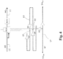
- the main line LP and the compensation line LS in the case where the main line comprises at least one buffer amplifier whose function is to restore the amplitude of the transmitted clock signal, the latter having tendency to weaken during its spread over the main line.
- the buffer amplifier (designated by the generic name BF on the figure 4 ) introduces an additional delay in the propagation of the clock edges.
- the duration T of propagation delay of the main line comprises the sum of this delay and of the inherent delay of the conductive line itself. It is then necessary to provide in each section of the compensation line LS an identical delay T, and it is therefore best to insert in each section a buffer amplifier LF identical to the amplifier inserted in the main line.
- the buffer amplifier is placed immediately at the input of the main line, and there is provided an LF amplifier inserted in the first section of the compensation line between the output S1 and the output S2, then another LF amplifier inserted into the second section between exit S2 and exit S3.
- the compensation line LS is extended, downstream of the output S3, by a section of line loaded by an amplifier.
- the compensation line can include, upstream of the output S1, an amplifier between the main line and the output S1.
- the load of the LF amplifier of the main line is formed by the main line itself loaded by the LF amplifier of the main line of the partial circuit located immediately downstream.
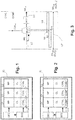
- the figure 5 represents an exemplary embodiment of the control lines of the multiplexer, making it possible to ensure the incrementation of the rank of the input of the multiplexer, and therefore the decrementation of the rank of the output selected by the multiplexer.
- the row i input is connected to the row N-i + 1 output of the compensation line and it is then the clock signal present on this output which will be transmitted to the output of the multiplexer.
- FIG. 5 there is shown in solid lines the connection between a multiplexer input and the selected output, and in dotted lines the connections with the non-selected outputs, and this for each of the three partial circuits shown.
- the configuration can be transposed to N partial circuits, then using N control lines for the multiplexers.
- the increment circuit perhaps, as shown in figure 5 , simply a circuit for circular permutation of the control lines: a row of any rank j in a partial circuit of rank i becomes a line of rank j + 1 in the partial circuit of rank i + 1.
- the row of row i in the partial circuit of row i selects the output of row N-i + 1 of this partial circuit, then extends into a line of row i + 1 in the following circuit of row i + 1 and it selects the output of rank Ni of this next circuit.
- incrementation circuits could be provided, using in particular shift registers whose incrementation is ensured by the partial circuit so that, after an initialization phase of the integrated circuit, the shift registers contain codes (001, 010, 100) different for each partial circuit, these codes controlling the selection of different inputs of the multiplexer.
- the multiplexer can also decode more conventional counting codes such as binary (00, 01, 10) or Gray (00, 01, 11) codes, in particular if shift registers are used.
- the invention applies mainly to integrated circuits formed by photorepetition, but can more generally be applied to any integrated circuit formed by a plurality of identical adjacent patterns, independently of their mode of manufacture.
Landscapes
- Physics & Mathematics (AREA)
- Engineering & Computer Science (AREA)
- Theoretical Computer Science (AREA)
- Nonlinear Science (AREA)
- General Engineering & Computer Science (AREA)
- General Physics & Mathematics (AREA)
- Design And Manufacture Of Integrated Circuits (AREA)
- Semiconductor Integrated Circuits (AREA)
- Pulse Circuits (AREA)
- Manipulation Of Pulses (AREA)
Claims (4)
- Integrierter Schaltkreis, beinhaltend N benachbarte, sämtlich identische Motive, welche N identischen benachbarten Teilschaltkreisen (C1, C2, C3) des Ranges i = 1 bis i = N in der geografischen Abfolge der Teilschaltkreise entsprechen, wobei jeder Teilschaltkreis einen vorgelagerten Uhrsignal-Eingang (EHAmi), einen nachgelagerten Uhrsignal-Ausgang (SHAv) und eine Hauptleitung (LP) beinhaltet, welche sich zwischen dem vorgelagerten Uhrsignal-Eingang (EHAmi) und dem nachgelagerten Uhrsignal-Ausgang (SHAv) erstreckt und eine Laufzeitverzögerung mit einer Dauer T einbringt, wobei der nachgelagerte Uhrsignal-Ausgang (SHAv) eines jeden Teilschaltkreises, ausgenommen desjenigen mit Rang N, direkt mit dem vorgelagerten Uhrsignal-Eingang (EHAmi) des unmittelbar nachfolgenden Teilschaltkreises in einer Weise verbunden ist, dass die Hauptleitungen (LP) der Teilschaltkreise die Kaskadenübertragung eines Mastersignals (CLK) ermöglichen, welches an dem Teilschaltkreis des Ranges 1 empfangen wurde, dadurch gekennzeichnet, dass er in jedem Teilschaltkreis des Ranges i Folgendes beinhaltet:- eine Kompensationsleitung (LS) mit N aufeinanderfolgenden Ausgängen (S1, S2, S3) des Ranges i = 1 bis N, verbunden mit der Hauptleitung (LP) das Teilschaltkreises, und welche eine Laufzeitverzögerung mit einer Dauer T zwischen den aufeinanderfolgenden Ausgängen herstellt,- einen Multiplexer (MUX) mit N jeweils mit jedem der N Ausgänge der Kompensationsleitung verbundenen Eingängen, und- Steuerleitungen (LC) des Multiplexers, welche angeordnet sind, um denjenigen Eingang des Ranges i des Multiplexers auszuwählen, welcher mit dem Ausgang des Ranges N-i+1 unter den N Ausgängen der Kompensationsleitung verbunden ist,wobei der Ausgang des Multiplexers des Teilschaltkreises des Ranges i somit ein lokales Signal (ClkLi) für diesen Teilschaltkreis bereitstellt;
und dadurch, dass:- die Steuerleitungen des Multiplexers des Teilschaltkreises des Ranges 1 konfiguriert sind, um ein Signal zur Auswahl des Eingangs des Ranges N dieses Multiplexers zu empfangen und um dieses Signal von einem Multiplexer an den nächsten zu propagieren, wobei sie dieses jedes Mal ändern, um den Rang des gewählten Eingangs um eine Einheit zu inkrementieren, damit die Steuerleitungen, welche am Multiplexer des Teilschaltkreises des Ranges i enden, den Ausgang des Ranges N-i+1 der Kompensationsleitung auswählen und an den Multiplexer des Teilschaltkreises des Ranges i+1 einen Auswahlbefehl des Ausgangs des Ranges N-i übertragen. - Integrierter Schaltkreis nach Anspruch 1, dadurch gekennzeichnet, dass das Mastersignal ein allgemeines Uhrsignal ist, und dass das vom Multiplexer des Ranges i stammende lokale Signal ein lokales Uhrsignal für den Teilschaltkreis des Ranges i ist.
- Integrierter Schaltkreis nach einem der Ansprüche 1 und 2, dadurch gekennzeichnet, dass die Steuerleitungen des Multiplexers des Teilschaltkreises des Ranges i Folgendes sind:- N an der Zahl,- so konfiguriert, dass die Aktivierung einer Steuerleitung das Ranges i, wobei die restlichen Steuerleitungen inaktiv sind, die Auswahl des Ranges N-i+1 der Kompensationsleitung ermöglicht, und- direkt mit den Steuerleitungen des Multiplexers des Schaltkreises des Ranges i+1 mit einer Kreispermutation verbunden, damit die aktive Steuerleitung des Ranges i des Multiplexers des Schaltkreises des Ranges i mit einer Steuerleitung des Ranges i+1 des Multiplexers des Schaltkreises des Ranges i+1 verbunden ist, wobei letztere Leitung konfiguriert ist, um, wenn sie aktiv ist, den Ausgang des Ranges N-i der Kompensationsleitung des Teilschaltkreises des Ranges i+1 auszuwählen.
- Integrierter Schaltkreis nach einem der Ansprüche 1 bis 3, dadurch gekennzeichnet, dass ein jeweiliger Pufferverstärker (BF) in die Hauptleitung eingefügt ist, und ein jeweiliger identischer Pufferverstärker (BF) in die Kompensationsleitung (LS) zwischen jedem Ausgang dieser Leitung und dem Ausgang des unmittelbar darauffolgenden Ranges der Leitung eingefügt ist.
Applications Claiming Priority (1)
| Application Number | Priority Date | Filing Date | Title |
|---|---|---|---|
| FR1457486A FR3024619B1 (fr) | 2014-08-01 | 2014-08-01 | Circuit integre photorepete avec compensation des retards de propagation de signaux, notamment de signaux d'horloge |
Publications (2)
| Publication Number | Publication Date |
|---|---|
| EP2980992A1 EP2980992A1 (de) | 2016-02-03 |
| EP2980992B1 true EP2980992B1 (de) | 2020-07-22 |
Family
ID=52807848
Family Applications (1)
| Application Number | Title | Priority Date | Filing Date |
|---|---|---|---|
| EP15179024.3A Active EP2980992B1 (de) | 2014-08-01 | 2015-07-30 | Integrierter lithografisch vervielfältigter schaltkreis mit kompensation der laufzeitverzögerungen von signalen, insbesondere von taktsignalen |
Country Status (5)
| Country | Link |
|---|---|
| US (1) | US9438218B2 (de) |
| EP (1) | EP2980992B1 (de) |
| JP (1) | JP6625363B2 (de) |
| ES (1) | ES2818079T3 (de) |
| FR (1) | FR3024619B1 (de) |
Families Citing this family (1)
| Publication number | Priority date | Publication date | Assignee | Title |
|---|---|---|---|---|
| FR3107150B1 (fr) | 2020-02-11 | 2022-01-21 | Pyxalis | Distribution et calibration de signaux synchronisés à travers un circuit intégré obtenu par photo-répétition |
Family Cites Families (14)
| Publication number | Priority date | Publication date | Assignee | Title |
|---|---|---|---|---|
| JPH0824143B2 (ja) * | 1989-02-08 | 1996-03-06 | 株式会社東芝 | 集積回路の配置配線方式 |
| US5586307A (en) * | 1993-06-30 | 1996-12-17 | Intel Corporation | Method and apparatus supplying synchronous clock signals to circuit components |
| FR2710800B1 (fr) * | 1993-09-27 | 1995-12-15 | Sgs Thomson Microelectronics | Ligne à retard numérique. |
| US5519350A (en) * | 1995-06-30 | 1996-05-21 | At&T Corp. | Circuitry for delivering a signal to different load elements located in an electronic system |
| US5881271A (en) * | 1996-12-31 | 1999-03-09 | Opti Inc. | System and method for clock management |
| EP1465344A1 (de) * | 2003-03-31 | 2004-10-06 | Infineon Technologies AG | Vorrichtung und Verfahren zur Konversion eines Eingangssignals |
| US7716511B2 (en) * | 2006-03-08 | 2010-05-11 | Freescale Semiconductor, Inc. | Dynamic timing adjustment in a circuit device |
| US8122275B2 (en) * | 2006-08-24 | 2012-02-21 | Altera Corporation | Write-leveling implementation in programmable logic devices |
| KR101470975B1 (ko) * | 2007-12-21 | 2014-12-09 | 램버스 인코포레이티드 | 메모리 시스템 내 기록 타이밍을 교정하기 위한 방법 및 장치 |
| FR2959901B1 (fr) * | 2010-05-04 | 2015-07-24 | E2V Semiconductors | Capteur d'image a matrice d'echantillonneurs |
| US8339166B2 (en) * | 2010-11-17 | 2012-12-25 | Advanced Micro Devices, Inc. | Clock gater with programmable delay |
| JP2013090313A (ja) * | 2011-10-24 | 2013-05-13 | Japan Radio Co Ltd | タイミング調整回路 |
| EP2680153B1 (de) * | 2012-06-29 | 2015-08-12 | Technische Universität Darmstadt | Verfahren und Vorrichtung zur Berichtigung einer Phasenverschiebung in einem zeitsynchronisierten System |
| JP2015008025A (ja) * | 2013-06-25 | 2015-01-15 | マイクロン テクノロジー, インク. | 半導体装置 |
-
2014
- 2014-08-01 FR FR1457486A patent/FR3024619B1/fr not_active Expired - Fee Related
-
2015
- 2015-07-30 ES ES15179024T patent/ES2818079T3/es active Active
- 2015-07-30 EP EP15179024.3A patent/EP2980992B1/de active Active
- 2015-07-31 US US14/815,292 patent/US9438218B2/en active Active
- 2015-07-31 JP JP2015152040A patent/JP6625363B2/ja active Active
Non-Patent Citations (1)
| Title |
|---|
| None * |
Also Published As
| Publication number | Publication date |
|---|---|
| FR3024619B1 (fr) | 2016-07-29 |
| US9438218B2 (en) | 2016-09-06 |
| JP6625363B2 (ja) | 2019-12-25 |
| EP2980992A1 (de) | 2016-02-03 |
| US20160036427A1 (en) | 2016-02-04 |
| ES2818079T3 (es) | 2021-04-09 |
| JP2016042573A (ja) | 2016-03-31 |
| FR3024619A1 (fr) | 2016-02-05 |
Similar Documents
| Publication | Publication Date | Title |
|---|---|---|
| FR2827684A1 (fr) | Controleur de memoire presentant une capacite d'ecriture 1x/mx | |
| EP3375092B1 (de) | Verfahren zur synchronisation eines datenwandlers mithilfe eines im nahfeld übertragenen signales | |
| EP0648017B1 (de) | Vorrichtung zur Überwachung der Phasenverschiebung zwischen zwei Taktsignalen | |
| EP1114377A1 (de) | Modulares datenerfassungssystem | |
| EP0146661A1 (de) | Elektrisches Untersuchungsverfahren zur Identifizierung einer defekten Zelle in einer Kette von Zellen, die ein Schieberegister bilden | |
| FR3050341A1 (fr) | Procede et dispositif de surveillance d'un chemin critique d'un circuit integre | |
| FR2652968A1 (fr) | Demultiplexeur. | |
| EP2980992B1 (de) | Integrierter lithografisch vervielfältigter schaltkreis mit kompensation der laufzeitverzögerungen von signalen, insbesondere von taktsignalen | |
| EP3231173B1 (de) | Vefahren zum synchronen verteilen eines digitalen signals an n identische und benachbart in einem integrierten schaltkreis angeordnete blöcke | |
| EP2366246B1 (de) | Integriertes schaltungsarray und insbesondere gross bemessener bildsensor | |
| EP3176713B1 (de) | Verfahren zum ausstatten der register eines integrierten schaltkreises für die detektion von timing-verletzungen | |
| EP1813952B1 (de) | Scantest | |
| EP1732241B1 (de) | Datenübertrasgungssystem und -Verfahren in einer elektronischen Schaltung | |
| EP2637310B1 (de) | Verzögerungsunempfindlicher asynchroner Schaltkreis | |
| EP3866341B1 (de) | Verteilung und kalibrierung von synchronisierten signalen durch eine integrierte schaltung, die durch fotowiederholung erhalten wird | |
| EP0400734B1 (de) | Programmierbares Binärsignal-Verzögerungsverfahren und Anwendung auf ein Fehlerkorrigierkode-Verfahren | |
| FR2919941A1 (fr) | Dispositif de test de circuit analogique | |
| EP1179739A1 (de) | Verfahren zum Testen einer intergrierten Schaltung mit flexibler Taktsteuerung | |
| EP0648018B1 (de) | Schaltung zur Anzeige der Phasenverhältnisse zwischen mehreren Signalen mit gleicher Frequenz und ihre Anwendung in einer Schaltung zur Korrektur der Phasen zwischen diesen Signalen | |
| EP3745234A1 (de) | Vorrichtung mit mehreren taktbereichen | |
| FR2642541A1 (fr) | Procede et dispositif de test de circuit integre numerique | |
| FR2888017A1 (fr) | Dispositif d'arbitrage asynchrone et microcontroleur comprenant un tel dispositif d'arbitrage | |
| FR2901362A1 (fr) | Circuit de qualification et de caracterisation d'une memoire embarquee dans un produit semi-conducteur | |
| FR2932006A1 (fr) | Circuit integre matriciel a decodage mixte | |
| EP1519285A1 (de) | Verbindungssystem für Rechnerbustypen, insbesondere für Rückwandleiterplatten |
Legal Events
| Date | Code | Title | Description |
|---|---|---|---|
| PUAI | Public reference made under article 153(3) epc to a published international application that has entered the european phase |
Free format text: ORIGINAL CODE: 0009012 |
|
| AK | Designated contracting states |
Kind code of ref document: A1 Designated state(s): AL AT BE BG CH CY CZ DE DK EE ES FI FR GB GR HR HU IE IS IT LI LT LU LV MC MK MT NL NO PL PT RO RS SE SI SK SM TR |
|
| AX | Request for extension of the european patent |
Extension state: BA ME |
|
| 17P | Request for examination filed |
Effective date: 20160729 |
|
| RBV | Designated contracting states (corrected) |
Designated state(s): AL AT BE BG CH CY CZ DE DK EE ES FI FR GB GR HR HU IE IS IT LI LT LU LV MC MK MT NL NO PL PT RO RS SE SI SK SM TR |
|
| STAA | Information on the status of an ep patent application or granted ep patent |
Free format text: STATUS: EXAMINATION IS IN PROGRESS |
|
| 17Q | First examination report despatched |
Effective date: 20181017 |
|
| GRAP | Despatch of communication of intention to grant a patent |
Free format text: ORIGINAL CODE: EPIDOSNIGR1 |
|
| STAA | Information on the status of an ep patent application or granted ep patent |
Free format text: STATUS: GRANT OF PATENT IS INTENDED |
|
| INTG | Intention to grant announced |
Effective date: 20200326 |
|
| GRAS | Grant fee paid |
Free format text: ORIGINAL CODE: EPIDOSNIGR3 |
|
| GRAA | (expected) grant |
Free format text: ORIGINAL CODE: 0009210 |
|
| STAA | Information on the status of an ep patent application or granted ep patent |
Free format text: STATUS: THE PATENT HAS BEEN GRANTED |
|
| AK | Designated contracting states |
Kind code of ref document: B1 Designated state(s): AL AT BE BG CH CY CZ DE DK EE ES FI FR GB GR HR HU IE IS IT LI LT LU LV MC MK MT NL NO PL PT RO RS SE SI SK SM TR |
|
| REG | Reference to a national code |
Ref country code: GB Ref legal event code: FG4D Free format text: NOT ENGLISH |
|
| REG | Reference to a national code |
Ref country code: CH Ref legal event code: EP |
|
| REG | Reference to a national code |
Ref country code: DE Ref legal event code: R096 Ref document number: 602015056048 Country of ref document: DE |
|
| REG | Reference to a national code |
Ref country code: AT Ref legal event code: REF Ref document number: 1294352 Country of ref document: AT Kind code of ref document: T Effective date: 20200815 |
|
| REG | Reference to a national code |
Ref country code: IE Ref legal event code: FG4D Free format text: LANGUAGE OF EP DOCUMENT: FRENCH |
|
| REG | Reference to a national code |
Ref country code: NL Ref legal event code: FP |
|
| REG | Reference to a national code |
Ref country code: LT Ref legal event code: MG4D |
|
| REG | Reference to a national code |
Ref country code: AT Ref legal event code: MK05 Ref document number: 1294352 Country of ref document: AT Kind code of ref document: T Effective date: 20200722 |
|
| PG25 | Lapsed in a contracting state [announced via postgrant information from national office to epo] |
Ref country code: HR Free format text: LAPSE BECAUSE OF FAILURE TO SUBMIT A TRANSLATION OF THE DESCRIPTION OR TO PAY THE FEE WITHIN THE PRESCRIBED TIME-LIMIT Effective date: 20200722 Ref country code: AT Free format text: LAPSE BECAUSE OF FAILURE TO SUBMIT A TRANSLATION OF THE DESCRIPTION OR TO PAY THE FEE WITHIN THE PRESCRIBED TIME-LIMIT Effective date: 20200722 Ref country code: PT Free format text: LAPSE BECAUSE OF FAILURE TO SUBMIT A TRANSLATION OF THE DESCRIPTION OR TO PAY THE FEE WITHIN THE PRESCRIBED TIME-LIMIT Effective date: 20201123 Ref country code: NO Free format text: LAPSE BECAUSE OF FAILURE TO SUBMIT A TRANSLATION OF THE DESCRIPTION OR TO PAY THE FEE WITHIN THE PRESCRIBED TIME-LIMIT Effective date: 20201022 Ref country code: LT Free format text: LAPSE BECAUSE OF FAILURE TO SUBMIT A TRANSLATION OF THE DESCRIPTION OR TO PAY THE FEE WITHIN THE PRESCRIBED TIME-LIMIT Effective date: 20200722 Ref country code: GR Free format text: LAPSE BECAUSE OF FAILURE TO SUBMIT A TRANSLATION OF THE DESCRIPTION OR TO PAY THE FEE WITHIN THE PRESCRIBED TIME-LIMIT Effective date: 20201023 Ref country code: BG Free format text: LAPSE BECAUSE OF FAILURE TO SUBMIT A TRANSLATION OF THE DESCRIPTION OR TO PAY THE FEE WITHIN THE PRESCRIBED TIME-LIMIT Effective date: 20201022 Ref country code: FI Free format text: LAPSE BECAUSE OF FAILURE TO SUBMIT A TRANSLATION OF THE DESCRIPTION OR TO PAY THE FEE WITHIN THE PRESCRIBED TIME-LIMIT Effective date: 20200722 Ref country code: SE Free format text: LAPSE BECAUSE OF FAILURE TO SUBMIT A TRANSLATION OF THE DESCRIPTION OR TO PAY THE FEE WITHIN THE PRESCRIBED TIME-LIMIT Effective date: 20200722 |
|
| PG25 | Lapsed in a contracting state [announced via postgrant information from national office to epo] |
Ref country code: LV Free format text: LAPSE BECAUSE OF FAILURE TO SUBMIT A TRANSLATION OF THE DESCRIPTION OR TO PAY THE FEE WITHIN THE PRESCRIBED TIME-LIMIT Effective date: 20200722 Ref country code: RS Free format text: LAPSE BECAUSE OF FAILURE TO SUBMIT A TRANSLATION OF THE DESCRIPTION OR TO PAY THE FEE WITHIN THE PRESCRIBED TIME-LIMIT Effective date: 20200722 Ref country code: PL Free format text: LAPSE BECAUSE OF FAILURE TO SUBMIT A TRANSLATION OF THE DESCRIPTION OR TO PAY THE FEE WITHIN THE PRESCRIBED TIME-LIMIT Effective date: 20200722 Ref country code: IS Free format text: LAPSE BECAUSE OF FAILURE TO SUBMIT A TRANSLATION OF THE DESCRIPTION OR TO PAY THE FEE WITHIN THE PRESCRIBED TIME-LIMIT Effective date: 20201122 |
|
| REG | Reference to a national code |
Ref country code: CH Ref legal event code: PL |
|
| REG | Reference to a national code |
Ref country code: ES Ref legal event code: FG2A Ref document number: 2818079 Country of ref document: ES Kind code of ref document: T3 Effective date: 20210409 |
|
| REG | Reference to a national code |
Ref country code: DE Ref legal event code: R097 Ref document number: 602015056048 Country of ref document: DE |
|
| PG25 | Lapsed in a contracting state [announced via postgrant information from national office to epo] |
Ref country code: MC Free format text: LAPSE BECAUSE OF FAILURE TO SUBMIT A TRANSLATION OF THE DESCRIPTION OR TO PAY THE FEE WITHIN THE PRESCRIBED TIME-LIMIT Effective date: 20200722 Ref country code: LI Free format text: LAPSE BECAUSE OF NON-PAYMENT OF DUE FEES Effective date: 20200731 Ref country code: LU Free format text: LAPSE BECAUSE OF NON-PAYMENT OF DUE FEES Effective date: 20200730 Ref country code: EE Free format text: LAPSE BECAUSE OF FAILURE TO SUBMIT A TRANSLATION OF THE DESCRIPTION OR TO PAY THE FEE WITHIN THE PRESCRIBED TIME-LIMIT Effective date: 20200722 Ref country code: RO Free format text: LAPSE BECAUSE OF FAILURE TO SUBMIT A TRANSLATION OF THE DESCRIPTION OR TO PAY THE FEE WITHIN THE PRESCRIBED TIME-LIMIT Effective date: 20200722 Ref country code: SM Free format text: LAPSE BECAUSE OF FAILURE TO SUBMIT A TRANSLATION OF THE DESCRIPTION OR TO PAY THE FEE WITHIN THE PRESCRIBED TIME-LIMIT Effective date: 20200722 Ref country code: CH Free format text: LAPSE BECAUSE OF NON-PAYMENT OF DUE FEES Effective date: 20200731 Ref country code: CZ Free format text: LAPSE BECAUSE OF FAILURE TO SUBMIT A TRANSLATION OF THE DESCRIPTION OR TO PAY THE FEE WITHIN THE PRESCRIBED TIME-LIMIT Effective date: 20200722 Ref country code: DK Free format text: LAPSE BECAUSE OF FAILURE TO SUBMIT A TRANSLATION OF THE DESCRIPTION OR TO PAY THE FEE WITHIN THE PRESCRIBED TIME-LIMIT Effective date: 20200722 Ref country code: IT Free format text: LAPSE BECAUSE OF FAILURE TO SUBMIT A TRANSLATION OF THE DESCRIPTION OR TO PAY THE FEE WITHIN THE PRESCRIBED TIME-LIMIT Effective date: 20200722 |
|
| PLBE | No opposition filed within time limit |
Free format text: ORIGINAL CODE: 0009261 |
|
| STAA | Information on the status of an ep patent application or granted ep patent |
Free format text: STATUS: NO OPPOSITION FILED WITHIN TIME LIMIT |
|
| PG25 | Lapsed in a contracting state [announced via postgrant information from national office to epo] |
Ref country code: AL Free format text: LAPSE BECAUSE OF FAILURE TO SUBMIT A TRANSLATION OF THE DESCRIPTION OR TO PAY THE FEE WITHIN THE PRESCRIBED TIME-LIMIT Effective date: 20200722 |
|
| 26N | No opposition filed |
Effective date: 20210423 |
|
| PG25 | Lapsed in a contracting state [announced via postgrant information from national office to epo] |
Ref country code: SK Free format text: LAPSE BECAUSE OF FAILURE TO SUBMIT A TRANSLATION OF THE DESCRIPTION OR TO PAY THE FEE WITHIN THE PRESCRIBED TIME-LIMIT Effective date: 20200722 |
|
| PG25 | Lapsed in a contracting state [announced via postgrant information from national office to epo] |
Ref country code: SI Free format text: LAPSE BECAUSE OF FAILURE TO SUBMIT A TRANSLATION OF THE DESCRIPTION OR TO PAY THE FEE WITHIN THE PRESCRIBED TIME-LIMIT Effective date: 20200722 Ref country code: IE Free format text: LAPSE BECAUSE OF NON-PAYMENT OF DUE FEES Effective date: 20200730 |
|
| PG25 | Lapsed in a contracting state [announced via postgrant information from national office to epo] |
Ref country code: TR Free format text: LAPSE BECAUSE OF FAILURE TO SUBMIT A TRANSLATION OF THE DESCRIPTION OR TO PAY THE FEE WITHIN THE PRESCRIBED TIME-LIMIT Effective date: 20200722 Ref country code: MT Free format text: LAPSE BECAUSE OF FAILURE TO SUBMIT A TRANSLATION OF THE DESCRIPTION OR TO PAY THE FEE WITHIN THE PRESCRIBED TIME-LIMIT Effective date: 20200722 Ref country code: CY Free format text: LAPSE BECAUSE OF FAILURE TO SUBMIT A TRANSLATION OF THE DESCRIPTION OR TO PAY THE FEE WITHIN THE PRESCRIBED TIME-LIMIT Effective date: 20200722 |
|
| PG25 | Lapsed in a contracting state [announced via postgrant information from national office to epo] |
Ref country code: MK Free format text: LAPSE BECAUSE OF FAILURE TO SUBMIT A TRANSLATION OF THE DESCRIPTION OR TO PAY THE FEE WITHIN THE PRESCRIBED TIME-LIMIT Effective date: 20200722 |
|
| PGFP | Annual fee paid to national office [announced via postgrant information from national office to epo] |
Ref country code: GB Payment date: 20250619 Year of fee payment: 11 |
|
| PGFP | Annual fee paid to national office [announced via postgrant information from national office to epo] |
Ref country code: NL Payment date: 20250627 Year of fee payment: 11 Ref country code: BE Payment date: 20250619 Year of fee payment: 11 |
|
| PGFP | Annual fee paid to national office [announced via postgrant information from national office to epo] |
Ref country code: FR Payment date: 20250623 Year of fee payment: 11 |
|
| PGFP | Annual fee paid to national office [announced via postgrant information from national office to epo] |
Ref country code: ES Payment date: 20250805 Year of fee payment: 11 |
|
| PGFP | Annual fee paid to national office [announced via postgrant information from national office to epo] |
Ref country code: DE Payment date: 20250618 Year of fee payment: 11 |