EP2999001A2 - Einbringung von abstandhaltern an den seiten eines transistor-gates - Google Patents
Einbringung von abstandhaltern an den seiten eines transistor-gates Download PDFInfo
- Publication number
- EP2999001A2 EP2999001A2 EP15184982.5A EP15184982A EP2999001A2 EP 2999001 A2 EP2999001 A2 EP 2999001A2 EP 15184982 A EP15184982 A EP 15184982A EP 2999001 A2 EP2999001 A2 EP 2999001A2
- Authority
- EP
- European Patent Office
- Prior art keywords
- layer
- etching
- dielectric layer
- surface layer
- gate
- Prior art date
- Legal status (The legal status is an assumption and is not a legal conclusion. Google has not performed a legal analysis and makes no representation as to the accuracy of the status listed.)
- Granted
Links
Images


Classifications
-
- H—ELECTRICITY
- H10—SEMICONDUCTOR DEVICES; ELECTRIC SOLID-STATE DEVICES NOT OTHERWISE PROVIDED FOR
- H10D—INORGANIC ELECTRIC SEMICONDUCTOR DEVICES
- H10D64/00—Electrodes of devices having potential barriers
- H10D64/01—Manufacture or treatment
- H10D64/021—Manufacture or treatment using multiple gate spacer layers, e.g. bilayered sidewall spacers
-
- H—ELECTRICITY
- H10—SEMICONDUCTOR DEVICES; ELECTRIC SOLID-STATE DEVICES NOT OTHERWISE PROVIDED FOR
- H10D—INORGANIC ELECTRIC SEMICONDUCTOR DEVICES
- H10D30/00—Field-effect transistors [FET]
- H10D30/01—Manufacture or treatment
- H10D30/021—Manufacture or treatment of FETs having insulated gates [IGFET]
- H10D30/027—Manufacture or treatment of FETs having insulated gates [IGFET] of lateral single-gate IGFETs
- H10D30/0275—Manufacture or treatment of FETs having insulated gates [IGFET] of lateral single-gate IGFETs forming single crystalline semiconductor source or drain regions resulting in recessed gates, e.g. forming raised source or drain regions
-
- H—ELECTRICITY
- H10—SEMICONDUCTOR DEVICES; ELECTRIC SOLID-STATE DEVICES NOT OTHERWISE PROVIDED FOR
- H10D—INORGANIC ELECTRIC SEMICONDUCTOR DEVICES
- H10D64/00—Electrodes of devices having potential barriers
- H10D64/01—Manufacture or treatment
- H10D64/015—Manufacture or treatment removing at least parts of gate spacers, e.g. disposable spacers
-
- H—ELECTRICITY
- H10—SEMICONDUCTOR DEVICES; ELECTRIC SOLID-STATE DEVICES NOT OTHERWISE PROVIDED FOR
- H10D—INORGANIC ELECTRIC SEMICONDUCTOR DEVICES
- H10D64/00—Electrodes of devices having potential barriers
- H10D64/20—Electrodes characterised by their shapes, relative sizes or dispositions
- H10D64/27—Electrodes not carrying the current to be rectified, amplified, oscillated or switched, e.g. gates
- H10D64/311—Gate electrodes for field-effect devices
- H10D64/411—Gate electrodes for field-effect devices for FETs
- H10D64/511—Gate electrodes for field-effect devices for FETs for IGFETs
- H10D64/514—Gate electrodes for field-effect devices for FETs for IGFETs characterised by the insulating layers
-
- H—ELECTRICITY
- H10—SEMICONDUCTOR DEVICES; ELECTRIC SOLID-STATE DEVICES NOT OTHERWISE PROVIDED FOR
- H10D—INORGANIC ELECTRIC SEMICONDUCTOR DEVICES
- H10D64/00—Electrodes of devices having potential barriers
- H10D64/60—Electrodes characterised by their materials
- H10D64/66—Electrodes having a conductor capacitively coupled to a semiconductor by an insulator, e.g. MIS electrodes
- H10D64/68—Electrodes having a conductor capacitively coupled to a semiconductor by an insulator, e.g. MIS electrodes characterised by the insulator, e.g. by the gate insulator
- H10D64/691—Electrodes having a conductor capacitively coupled to a semiconductor by an insulator, e.g. MIS electrodes characterised by the insulator, e.g. by the gate insulator comprising metallic compounds, e.g. metal oxides or metal silicates
-
- H—ELECTRICITY
- H10—SEMICONDUCTOR DEVICES; ELECTRIC SOLID-STATE DEVICES NOT OTHERWISE PROVIDED FOR
- H10P—GENERIC PROCESSES OR APPARATUS FOR THE MANUFACTURE OR TREATMENT OF DEVICES COVERED BY CLASS H10
- H10P14/00—Formation of materials, e.g. in the shape of layers or pillars
- H10P14/40—Formation of materials, e.g. in the shape of layers or pillars of conductive or resistive materials
-
- H—ELECTRICITY
- H10—SEMICONDUCTOR DEVICES; ELECTRIC SOLID-STATE DEVICES NOT OTHERWISE PROVIDED FOR
- H10P—GENERIC PROCESSES OR APPARATUS FOR THE MANUFACTURE OR TREATMENT OF DEVICES COVERED BY CLASS H10
- H10P50/00—Etching of wafers, substrates or parts of devices
- H10P50/20—Dry etching; Plasma etching; Reactive-ion etching
- H10P50/28—Dry etching; Plasma etching; Reactive-ion etching of insulating materials
- H10P50/282—Dry etching; Plasma etching; Reactive-ion etching of insulating materials of inorganic materials
- H10P50/283—Dry etching; Plasma etching; Reactive-ion etching of insulating materials of inorganic materials by chemical means
-
- H—ELECTRICITY
- H10—SEMICONDUCTOR DEVICES; ELECTRIC SOLID-STATE DEVICES NOT OTHERWISE PROVIDED FOR
- H10P—GENERIC PROCESSES OR APPARATUS FOR THE MANUFACTURE OR TREATMENT OF DEVICES COVERED BY CLASS H10
- H10P50/00—Etching of wafers, substrates or parts of devices
- H10P50/73—Etching of wafers, substrates or parts of devices using masks for insulating materials
-
- H—ELECTRICITY
- H10—SEMICONDUCTOR DEVICES; ELECTRIC SOLID-STATE DEVICES NOT OTHERWISE PROVIDED FOR
- H10D—INORGANIC ELECTRIC SEMICONDUCTOR DEVICES
- H10D64/00—Electrodes of devices having potential barriers
- H10D64/60—Electrodes characterised by their materials
- H10D64/66—Electrodes having a conductor capacitively coupled to a semiconductor by an insulator, e.g. MIS electrodes
- H10D64/68—Electrodes having a conductor capacitively coupled to a semiconductor by an insulator, e.g. MIS electrodes characterised by the insulator, e.g. by the gate insulator
- H10D64/681—Electrodes having a conductor capacitively coupled to a semiconductor by an insulator, e.g. MIS electrodes characterised by the insulator, e.g. by the gate insulator having a compositional variation, e.g. multilayered
- H10D64/685—Electrodes having a conductor capacitively coupled to a semiconductor by an insulator, e.g. MIS electrodes characterised by the insulator, e.g. by the gate insulator having a compositional variation, e.g. multilayered being perpendicular to the channel plane
-
- H—ELECTRICITY
- H10—SEMICONDUCTOR DEVICES; ELECTRIC SOLID-STATE DEVICES NOT OTHERWISE PROVIDED FOR
- H10P—GENERIC PROCESSES OR APPARATUS FOR THE MANUFACTURE OR TREATMENT OF DEVICES COVERED BY CLASS H10
- H10P14/00—Formation of materials, e.g. in the shape of layers or pillars
- H10P14/60—Formation of materials, e.g. in the shape of layers or pillars of insulating materials
- H10P14/65—Formation of materials, e.g. in the shape of layers or pillars of insulating materials characterised by treatments performed before or after the formation of the materials
- H10P14/6516—Formation of materials, e.g. in the shape of layers or pillars of insulating materials characterised by treatments performed before or after the formation of the materials of treatments performed after formation of the materials
- H10P14/6518—Formation of materials, e.g. in the shape of layers or pillars of insulating materials characterised by treatments performed before or after the formation of the materials of treatments performed after formation of the materials by introduction of substances into an already-existing insulating layer
- H10P14/6519—Formation of materials, e.g. in the shape of layers or pillars of insulating materials characterised by treatments performed before or after the formation of the materials of treatments performed after formation of the materials by introduction of substances into an already-existing insulating layer the substance being oxygen
- H10P14/6522—Formation of materials, e.g. in the shape of layers or pillars of insulating materials characterised by treatments performed before or after the formation of the materials of treatments performed after formation of the materials by introduction of substances into an already-existing insulating layer the substance being oxygen introduced into a nitride material, e.g. changing SiN to SiON
-
- H—ELECTRICITY
- H10—SEMICONDUCTOR DEVICES; ELECTRIC SOLID-STATE DEVICES NOT OTHERWISE PROVIDED FOR
- H10P—GENERIC PROCESSES OR APPARATUS FOR THE MANUFACTURE OR TREATMENT OF DEVICES COVERED BY CLASS H10
- H10P14/00—Formation of materials, e.g. in the shape of layers or pillars
- H10P14/60—Formation of materials, e.g. in the shape of layers or pillars of insulating materials
- H10P14/65—Formation of materials, e.g. in the shape of layers or pillars of insulating materials characterised by treatments performed before or after the formation of the materials
- H10P14/6516—Formation of materials, e.g. in the shape of layers or pillars of insulating materials characterised by treatments performed before or after the formation of the materials of treatments performed after formation of the materials
- H10P14/6529—Formation of materials, e.g. in the shape of layers or pillars of insulating materials characterised by treatments performed before or after the formation of the materials of treatments performed after formation of the materials by exposure to a gas or vapour
- H10P14/6532—Formation of materials, e.g. in the shape of layers or pillars of insulating materials characterised by treatments performed before or after the formation of the materials of treatments performed after formation of the materials by exposure to a gas or vapour by exposure to a plasma
Definitions
- the present invention relates to transistors, particularly transistors of the MOS type (Metal Oxide Semiconductor) and more particularly the realization of the gate spacers of such transistors.
- MOS Metal Oxide Semiconductor
- microelectronics industry understood here as including nanotechnology, is concerned with the invention, in the use of field effect transistors and in particular MOSFET transistors widely used in integrated circuits.
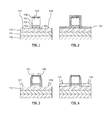
- the figure 1 is a sectional view of an example of this type of transistor in progress. It contains the source and drain zones 120, 121.
- the grid 100 conventionally consists of a stack of layers, a large part of which is still made of polycrystalline silicon 101.
- the formation of the source and drain zones 120, 121 is typically by ion implantation of dopants in the zones 120, 121, the gate 100 serving as a mask as mentioned above, thus preventing doping of the area of the transistor in which, depending on the voltages applied to the gate 100, will be able to develop the conduction channel 105 between source and drain.
- SOI silicon-on-insulator substrates
- SOI-developed substrate is characterized by the presence of a thin surface layer of monocrystalline silicon, of Germanium or of silicon-germanium 112 resting on a continuous insulating layer of oxide 111, in particular of silicon, called oxide buried or BOX acronym for "buried oxide layer".
- the layer 111 rests on the layer 110 which constitutes the body of the SOI substrate, often called the English word "bulk” to indicate that the starting substrate is very generally made of solid silicon.
- This structure offers many advantages for the realization of MOSFET transistors.
- the layers 103 and 104 constitute the gate oxide comprising most often in recent embodiments a layer 104 of a high-grade material. relative permittivity called "high-k".
- the layer 102 is a hard mask used to protect, at this stage of realization, the stack of the underlying grid layers.
- the surface layer 112, for example made of monocrystalline silicon, can be precisely controlled in terms of thickness and doping.
- FD fully depleted
- spacers 130 on the sides of the grid 100.
- the spacers 130 typically made of silicon nitride (SiN)
- SiN silicon nitride
- the spacers 130 are made in this technology without involving any photoengraving operation.
- the figure 2 shows the formation of a first nitride layer 131, in particular silicon nitride (Si N).
- This layer is then subjected, at the stage of figure 3 , at a strongly anisotropic etching so that the etching removes the portions of the layer 131 located on the surface layer 112 (which are generally horizontal, that is to say oriented perpendicularly to the thickness of the substrate 110) while preserving at least in part, the nitride on the non-horizontal parts and particularly on the parts forming the sidewalls (106, 107 of the grid 100).
- a first level of spacers constituted by the residual parts made of nitride covering the flanks 106, 107 is thus obtained.
- Second level spacers are then produced.
- a new layer of nitride 132 is deposited, as shown in FIG. figure 5 .
- the figure 6 illustrates an etching of the nitride layer 132 such that the layer 132 is preserved, at least in part, only on the sides of the grid, covering the spacers already formed at this level. Overall, these steps lead to spacers whose foot has a withdrawal.
- a new phase of epitaxy is then produced so that the source / drain zones 120, 121 grow around the grid 100, which is protected by the spacers 130 as shown in FIG. figure 7 .
- the document US-B1-6635938 also provides two layers of spacers whose horizontal portions are removed simultaneously to keep in place only the vertical portion around the grid flanks.
- the present invention makes it possible to meet at least some of the disadvantages of current techniques.
- the parameters of the final etching which is a selective etching relative to the surface layer, can thus be more freely adjusted so as to control, for example, the shape to be given to the stand of the spacers, or else to avoid an attack of the the surface layer, for example nanocrystalline silicon (but possibly also Germanium or silicon-germanium).
- the invention is thus compatible with technologies in which the thickness of the semiconductor layer is low, for example less than 5 nm, and the method can be applied to substrates of the silicon on insulator (SOI) type, including FDSOI (for Fully Depleted Silicon on Insulator).
- SOI silicon on insulator
- FDSOI Fully Depleted Silicon on Insulator
- the formation of the surface layer comprises a modification of the material of only a portion of the thickness of the dielectric layer. It is therefore not necessarily required to perform a deposition step to achieve the surface layer.
- the oxidation can be performed by plasma under isotropic or quasi-isotropic conditions so that the oxidized layer is in conformity.
- all the steps or at least some successive steps can be performed within the same reactor.
- the use of plasma technology thus makes it possible to avoid manipulations.
- the invention is also relative, in embodiments, to a raised source / drain structure transistor in which a gate and source and drain regions are located above a layer of a semiconductor material and which has spacers at the edges of the gate configured to isolate the gate from the source and drain areas.
- This transistor is preferably such that the spacers have a single layer of a dielectric material, preferably silicon nitride.
- the transistor may comprise at least partial coverage portions of the single layer of the spacers, preferably an oxide of the dielectric material of the single layer.
- the source and drain zones are located in a single layer of a material, said single layer being situated above the layer of a semiconductor material.
- the spacers comprise a foot zone above the layer of semiconductor material, the foot zone having a recess towards the side of the gate, so as to form a recess.
- Another aspect of the invention is a transistor, such as an MOS transistor, in which the gate spacers are partially covered with a surface layer of a material different from the material of the spacers, for example an oxide of the material of the spacers.
- a transistor can be obtained by the method of the invention.
- Another aspect of the invention relates to a method for producing a transistor in which the gate is located above a layer of a semiconductor material, said method comprising the production of spacers according to the production method. of spacers of the invention. It may include providing source and drain areas with epitaxial growth on the layer of semiconductor material.
- the term “over”, “overcomes” or “underlying” or their equivalent do not necessarily mean “in contact with”.
- the deposition of a first layer on a second layer does not necessarily mean that the two layers are in direct contact with one another, but that means that the first layer at least partially covers the second layer. being either directly in contact with it or separated from it by another layer or another element.
- the thicknesses are generally measured in directions perpendicular to the plane of the lower face of the layer to be etched or a substrate on which the lower layer is disposed. Thus, the thicknesses are generally taken in a vertical direction in the figures shown. On the other hand, the thickness of a layer covering a flank of a pattern is taken in a direction perpendicular to this flank.
- selective etching means the etching removal of a given material while preserving at least in part, by the selectivity of the process employed, other materials.
- surface layer corresponds to a layer that is formed, in particular by modifying the underlying layer or by a deposit on this underlying layer, at the surface of the electronic device after the formation of the underlying layer. . It is then partially removed to partially remove the underlying layer.
- the adjective “superficial” does not necessarily mean that the residual surface layer remains always on the surface of the device when the manufacture of the latter is finalized. It can be for example removed or covered.
- compliant is meant a layer geometry which has the same thickness, with manufacturing tolerances, an identical thickness despite changes in layer direction, for example at the level of the grid pattern sidewalls.
- dielectric corresponds to a material whose electrical conductivity is sufficiently low in the given application to serve as insulation.
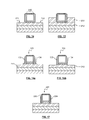
- the method of producing spacers according to the invention is illustrated by the Figures 9 to 14 .
- the method applies after the gates of the transistors have been formed, that is to say from a structure such as that illustrated by FIG. figure 8 which is not different, in this example, from that of the figure 1 already described.
- the method of the invention can in fact potentially be implemented from any MOSFET transistor structure after the grid patterns have been defined by photolithography.
- the figure 9 illustrates the first step of the process of the invention during which we will come to achieve the spacers in a single series of steps in contrast to the traditional method, briefly described in the chapter on the state of the art, which requires implementation two successive series of steps each comprising: the deposition of the material constituting the spacers, its etching and an epitaxial growth of the source / drain zones.
- a so-called “conformal” deposit is made over a thickness, for example ranging from 20 to 30 nm, preferably 25 nm.
- the deposit is consistent if it is done equally regardless of the orientation of the surfaces on which it is made.
- the deposition is preferably carried out by means of a so-called PECVD method, or a so-called LPCVD process, acronym for English “plasma-enhanced chemical vapor deposition”. low-pressure chemical vapor deposition ".
- PECVD method or a so-called LPCVD process, acronym for English "plasma-enhanced chemical vapor deposition”.
- low-pressure chemical vapor deposition ".
- the deposited layer 231 is of substantially equal thickness on the sides of the grid patterns and on the horizontal portions, that is to say those parallel to
- anisotropic etching of the layer 231 is then carried out, that is to say a substantially vertical etching of the deposited material, etching which is therefore perpendicular to the plane of the substrate and which does not etch, or very little, the blanks Grid patterns 206 and 207.
- This type of etching is advantageously made from a plasma in a capacitively coupled type (CCP) or inductively coupled type (ICP) etching reactor and preferably in a reactor of the latter. type.
- This anisotropic etching is intended to reduce the thickness of the layer 231 in the peripheral zones surrounding the gate 200 to a value corresponding to the thickness (for example between 10 and 15 nm) of the first deposit of the material constituting the spacers of the conventional method in which they are formed in two series of steps as discussed above.
- the figure 11 illustrates the result of the next step in which there is carried out a surface oxidation 232 of the layer 231 of the material intended to form the spacers.
- This oxidation is preferably produced in the same reactor as that of the anisotropic etching.
- the layer 232 of oxide or of another material can be obtained by deposition.
- the thickness thus produced can be between 2 and 10 nm, preferably 7 nm.
- the figure 12 shows the result of the next step at the end of which is left in place the oxidized layer 232 only on the sides of the grid patterns.
- This result is obtained by means of a very anisotropic vertical etching operation called "breakthrough" which is practiced for example in argon plasma (Ar) or carbon tetrafluoride (CF4) and which essentially burns all oxidized surfaces parallel to the plane of the substrate. Leaving at least partly in place the oxidized surfaces not parallel to the substrate at the sides 205, 206.
- the figure 13 shows the result of the step of lateral etching of the parts of the material forming the spacers which have been deoxidized in the previous step.
- This etching is selective with respect to the underlying semiconductor layer 212 and also vis-à-vis the remaining oxidized layer 234 which are therefore not etched significantly during this operation.
- This step ensures a removal of the layer 231 above the layer 212, outside the space occupied by the grid and the spacers. Typically, it is the portion of the layer 231 oriented parallel to the face of the substrate, horizontally in the case of the figures, or again the peripheral zone explained above.
- This step follows the etching of the layer 232 and is not simultaneous, so as to ensure a different selectivity of the two etchings.
- This step of etching the portion of the layer 231 out of the spacers can advantageously simultaneously, an etching of this material at the spacers (in particular at the right of the residual portion 234 of the surface layer 232.
- a lateral engraving at the foot of the spacers which reproduces the forms obtained with the standard process as shown on the figure 7 .
- Etching is here called lateral, in that it produces an attack substantially parallel to the substrate because of its selectivity.
- This etching is in fact preferably isotropic.
- the geometry of the shrinkage, in particular the flank of the shrinkage along the height h in figure 13 may be non-rectilinear. In practice, it may be in an arc.
- the bias voltage is preferentially pulsed at a frequency of 500 Hz with a duty cycle of 50%. Other pulsation conditions can be used: 200 Hz / 20%; 900 Hz / 90%; 200 Hz / 90%.
- the same reactor as before can be used.
- Lateral etching can also be done wet in a solution based on phosphoric acid (H3PO4).
- the etching rate of silicon nitride which is generally used for spacers, is 4 nm per minute.
- the temperature is for example between 80 ° C and 120 ° C and preferably 100 ° C. This chemistry has an infinite selectivity with respect to the oxide present on the residual portions 234 present on the flanks of the spacers. It is also chosen selective with respect to the material of the layer 212.
- the figure 14 shows a shape of the spacers 230 that can be obtained in practice with the method of the invention, the residual portions 234 having been removed, which is not mandatory but can be done, especially during a cleaning step, particularly if the material of the parts 234 is an oxide sensitive to the cleaning solution.
- the surface of the layer 212 from which the epitaxial growth is to be made is preferable to wet cleaning the surface of the layer 212 from which the epitaxial growth is to be made. Cleaning is preferably carried out using a solution based on hydrofluoric acid (HF), for example diluted to 0.5%, for 30 seconds. This cleaning is intended to remove the polymers and the native oxide layer on the surface of the semiconductor which is silicon (Si) or a compound of silicon and germanium (SiGe). In another embodiment, the portions 234 are held in place.
- HF hydrofluoric acid
- the figure 15 illustrates the step of selective epitaxial growth 235 of the source and drain zones that is performed next. As we have seen this operation is carried out only once with the method of the invention whereas it must be repeated a second time when using the standard method of forming the spacers.
- in-situ doping of these zones may be carried out, ie in the epitaxial reactor itself, by introducing the necessary doping species, such as boron, in gaseous form. (P-type doping) or arsenic (N-type doping).
- the necessary doping species such as boron, in gaseous form. (P-type doping) or arsenic (N-type doping).
- in-situ doping it will be possible, after formation of the epitaxial layer, to implant the doping species in an implanter.
- the material constituting the spacers may advantageously be a material with a lower relative permittivity (Low-k) than the silicon nitride which is conventionally used in order to reduce the parasitic capacitances of the transistor ( between drain / source on the one hand and the grid on the other hand).
- Low-k relative permittivity
- the figure 16a illustrates a problem that commonly occurs with the standard method of making spacers where it is difficult to control the etching of the first spacer without damaging the thin superficial semiconductor layer 212 of the substrate (such damage is illustrated in FIG. figure 16b ).
- "feet" 134 are often formed in a very undesirable manner at the bottom of the first spacers.
- Feet formation is no longer possible because it is possible to adjust the parameters of the etching plasma, in particular the etching time, without damaging the semiconductor layer 212, a layer from which it will be possible to proceed to an epitaxy of the zones. source and drain without defect.
Landscapes
- Insulated Gate Type Field-Effect Transistor (AREA)
- Chemical & Material Sciences (AREA)
- Chemical Kinetics & Catalysis (AREA)
- General Chemical & Material Sciences (AREA)
- Thin Film Transistor (AREA)
- Formation Of Insulating Films (AREA)
- Crystallography & Structural Chemistry (AREA)
Applications Claiming Priority (1)
| Application Number | Priority Date | Filing Date | Title |
|---|---|---|---|
| FR1458759A FR3025938B1 (fr) | 2014-09-17 | 2014-09-17 | Realisation d'espaceurs au niveau de flancs d'une grille de transistor |
Publications (3)
| Publication Number | Publication Date |
|---|---|
| EP2999001A2 true EP2999001A2 (de) | 2016-03-23 |
| EP2999001A3 EP2999001A3 (de) | 2016-04-13 |
| EP2999001B1 EP2999001B1 (de) | 2019-09-04 |
Family
ID=51842618
Family Applications (1)
| Application Number | Title | Priority Date | Filing Date |
|---|---|---|---|
| EP15184982.5A Active EP2999001B1 (de) | 2014-09-17 | 2015-09-14 | Einbringung von abstandhaltern an den seiten eines transistor-gates |
Country Status (3)
| Country | Link |
|---|---|
| US (1) | US9543409B2 (de) |
| EP (1) | EP2999001B1 (de) |
| FR (1) | FR3025938B1 (de) |
Cited By (1)
| Publication number | Priority date | Publication date | Assignee | Title |
|---|---|---|---|---|
| FR3065576A1 (fr) * | 2017-04-25 | 2018-10-26 | Commissariat A L'energie Atomique Et Aux Energies Alternatives | Procede de gravure d'une couche a base de sin |
Families Citing this family (11)
| Publication number | Priority date | Publication date | Assignee | Title |
|---|---|---|---|---|
| US10541102B2 (en) * | 2016-09-14 | 2020-01-21 | The Boeing Company | X-ray back scattering for inspection of part |
| CN106449762A (zh) * | 2016-12-16 | 2017-02-22 | 上海华力微电子有限公司 | 用于finfet间隔物成型的集成工艺 |
| US10283370B1 (en) * | 2018-03-01 | 2019-05-07 | Applied Materials, Inc. | Silicon addition for silicon nitride etching selectivity |
| US11088147B2 (en) | 2019-06-26 | 2021-08-10 | Micron Technology, Inc. | Apparatus with doped surfaces, and related methods with in situ doping |
| FR3098978A1 (fr) | 2019-07-18 | 2021-01-22 | Commissariat A L'energie Atomique Et Aux Energies Alternatives | procédé de fabrication de transistors |
| FR3098981A1 (fr) | 2019-07-18 | 2021-01-22 | Commissariat A L'energie Atomique Et Aux Energies Alternatives | procédé de fabrication de transistors |
| CN113745147A (zh) * | 2020-05-14 | 2021-12-03 | 上海功成半导体科技有限公司 | Fd-soi衬底结构、器件结构的制备方法 |
| CN113675135A (zh) * | 2020-05-14 | 2021-11-19 | 上海功成半导体科技有限公司 | Fd-soi衬底结构、器件结构的制备方法 |
| CN113675218A (zh) * | 2020-05-14 | 2021-11-19 | 上海功成半导体科技有限公司 | Fd-soi衬底结构及器件结构 |
| CN114256345A (zh) * | 2020-09-21 | 2022-03-29 | 上海华力集成电路制造有限公司 | 一种fdsoi器件结构及其制备方法 |
| FR3120157B1 (fr) | 2021-02-25 | 2023-04-14 | Commissariat Energie Atomique | Procédé de gravure d’une couche diélectrique tridimensionnelle |
Citations (3)
| Publication number | Priority date | Publication date | Assignee | Title |
|---|---|---|---|---|
| WO2002029881A1 (fr) | 2000-10-06 | 2002-04-11 | Stmicroelectronics S.A. | Transistors mos miniaturises de type ldd |
| US6635938B1 (en) | 2000-03-07 | 2003-10-21 | Mitsubishi Denki Kabushiki Kaisha | Semiconductor device and manufacturing method thereof |
| US20040132258A1 (en) | 2003-01-07 | 2004-07-08 | You-Seung Jin | MOSFET and method of fabricating the same |
Family Cites Families (8)
| Publication number | Priority date | Publication date | Assignee | Title |
|---|---|---|---|---|
| US6232641B1 (en) * | 1998-05-29 | 2001-05-15 | Kabushiki Kaisha Toshiba | Semiconductor apparatus having elevated source and drain structure and manufacturing method therefor |
| US6593618B2 (en) * | 2000-11-28 | 2003-07-15 | Kabushiki Kaisha Toshiba | MIS semiconductor device having an elevated source/drain structure |
| US6991979B2 (en) * | 2003-09-22 | 2006-01-31 | International Business Machines Corporation | Method for avoiding oxide undercut during pre-silicide clean for thin spacer FETs |
| KR101025740B1 (ko) * | 2003-12-19 | 2011-04-04 | 주식회사 하이닉스반도체 | 증착 접합을 갖는 트랜지스터의 제조 방법 |
| US7303983B2 (en) * | 2006-01-13 | 2007-12-04 | Freescale Semiconductor, Inc. | ALD gate electrode |
| JP2008072032A (ja) * | 2006-09-15 | 2008-03-27 | Toshiba Corp | 半導体装置の製造方法 |
| US8664125B2 (en) * | 2011-12-23 | 2014-03-04 | Tokyo Electron Limited | Highly selective spacer etch process with reduced sidewall spacer slimming |
| US9614053B2 (en) * | 2013-12-05 | 2017-04-04 | Taiwan Semiconductor Manufacturing Company, Ltd. | Spacers with rectangular profile and methods of forming the same |
-
2014
- 2014-09-17 FR FR1458759A patent/FR3025938B1/fr not_active Expired - Fee Related
-
2015
- 2015-09-14 EP EP15184982.5A patent/EP2999001B1/de active Active
- 2015-09-16 US US14/855,834 patent/US9543409B2/en active Active
Patent Citations (3)
| Publication number | Priority date | Publication date | Assignee | Title |
|---|---|---|---|---|
| US6635938B1 (en) | 2000-03-07 | 2003-10-21 | Mitsubishi Denki Kabushiki Kaisha | Semiconductor device and manufacturing method thereof |
| WO2002029881A1 (fr) | 2000-10-06 | 2002-04-11 | Stmicroelectronics S.A. | Transistors mos miniaturises de type ldd |
| US20040132258A1 (en) | 2003-01-07 | 2004-07-08 | You-Seung Jin | MOSFET and method of fabricating the same |
Cited By (3)
| Publication number | Priority date | Publication date | Assignee | Title |
|---|---|---|---|---|
| FR3065576A1 (fr) * | 2017-04-25 | 2018-10-26 | Commissariat A L'energie Atomique Et Aux Energies Alternatives | Procede de gravure d'une couche a base de sin |
| EP3396704A1 (de) * | 2017-04-25 | 2018-10-31 | Commissariat à l'Energie Atomique et aux Energies Alternatives | Gravierverfahren einer schicht auf sin-basis |
| US10446408B2 (en) | 2017-04-25 | 2019-10-15 | Commissariat A L'energie Atomique Et Aux Energies Alternatives | Process for etching a SiN-based layer |
Also Published As
| Publication number | Publication date |
|---|---|
| EP2999001B1 (de) | 2019-09-04 |
| EP2999001A3 (de) | 2016-04-13 |
| FR3025938B1 (fr) | 2018-05-25 |
| US20160079388A1 (en) | 2016-03-17 |
| FR3025938A1 (fr) | 2016-03-18 |
| US9543409B2 (en) | 2017-01-10 |
Similar Documents
| Publication | Publication Date | Title |
|---|---|---|
| EP2999001B1 (de) | Einbringung von abstandhaltern an den seiten eines transistor-gates | |
| EP2876677B1 (de) | Verfahren zur Bildung von Abstandhaltern eines Gates eines Transistors | |
| EP2939262B1 (de) | Mikroelektronisches verfahren zum ätzen einer schicht | |
| EP2975645A1 (de) | Verfahren zur herstellung von abstandshaltern eines gates eines transistors | |
| EP2750170A1 (de) | Verfahren zur Bildung von Abstandhaltern eines Gates eines Transistors | |
| EP3261124B1 (de) | Verfahren zur bildung von abstandhaltern eines gates eines transistors | |
| FR3043837A1 (fr) | Procede de realisation de transistor a nanofil semi-conducteur et comprenant une grille et des espaceurs auto-alignes | |
| EP2610915A1 (de) | Transistor und Herstellungsverfahren eines Transistors | |
| FR3046290B1 (fr) | Methode de realisation d'espaceurs a faible permittivite | |
| WO2014037410A1 (fr) | Procédé de gravure d'un matériau semiconducteur cristallin par implantation ionique puis gravure chimique à base de chlorure d'hydrogène | |
| EP3174092B1 (de) | Verfahren zur bildung von abstandhaltern eines gates eines transistors | |
| EP3671857B1 (de) | Herstellungsverfahren eines transistors mit erhöhter source und drain | |
| EP3506336B1 (de) | Ätzverfahren einer dielektrischen 3d-schicht | |
| EP3107118B1 (de) | Verfahren zur bildung von abstandhaltern eines gates eines transistors | |
| FR3080486A1 (fr) | Procede de formation d'un dispositif microelectronique | |
| EP3246948B1 (de) | Verfahren zur herstellung von transistoren, die unterschiedliche eigenschaften aufweisen, auf demselben substrat | |
| FR3047352A1 (fr) | Procede de fabrication d'un transistor a dopant localise a l'aplomb de la grille | |
| FR2995135A1 (fr) | Procede de realisation de transistors fet | |
| EP3671815B1 (de) | Gravurverfahren einer dielektrischen 3d-schicht | |
| EP2998998B1 (de) | Ätzungsverfahren an der oberfläche einer 3d-struktur | |
| FR3023058A1 (fr) | Procede de realisation d'un dispositif microelectronique | |
| FR3098981A1 (fr) | procédé de fabrication de transistors | |
| FR3120158A1 (fr) | Procédé de formation des espaceurs d'une grille d'un transistor | |
| EP4053883B1 (de) | Verfahren zum ätzen einer dielektrischen dreidimensionalen schicht | |
| EP4002482B1 (de) | Verfahren zur herstellung eines bereichs, der mit einer mikroelektronischen vorrichtung dotiert ist |
Legal Events
| Date | Code | Title | Description |
|---|---|---|---|
| PUAL | Search report despatched |
Free format text: ORIGINAL CODE: 0009013 |
|
| PUAI | Public reference made under article 153(3) epc to a published international application that has entered the european phase |
Free format text: ORIGINAL CODE: 0009012 |
|
| AK | Designated contracting states |
Kind code of ref document: A2 Designated state(s): AL AT BE BG CH CY CZ DE DK EE ES FI FR GB GR HR HU IE IS IT LI LT LU LV MC MK MT NL NO PL PT RO RS SE SI SK SM TR |
|
| AX | Request for extension of the european patent |
Extension state: BA ME |
|
| AK | Designated contracting states |
Kind code of ref document: A3 Designated state(s): AL AT BE BG CH CY CZ DE DK EE ES FI FR GB GR HR HU IE IS IT LI LT LU LV MC MK MT NL NO PL PT RO RS SE SI SK SM TR |
|
| AX | Request for extension of the european patent |
Extension state: BA ME |
|
| RIC1 | Information provided on ipc code assigned before grant |
Ipc: H01L 21/336 20060101ALI20160310BHEP Ipc: H01L 29/78 20060101AFI20160310BHEP Ipc: H01L 29/66 20060101ALI20160310BHEP |
|
| 17P | Request for examination filed |
Effective date: 20160914 |
|
| RBV | Designated contracting states (corrected) |
Designated state(s): AL AT BE BG CH CY CZ DE DK EE ES FI FR GB GR HR HU IE IS IT LI LT LU LV MC MK MT NL NO PL PT RO RS SE SI SK SM TR |
|
| GRAP | Despatch of communication of intention to grant a patent |
Free format text: ORIGINAL CODE: EPIDOSNIGR1 |
|
| STAA | Information on the status of an ep patent application or granted ep patent |
Free format text: STATUS: GRANT OF PATENT IS INTENDED |
|
| RIC1 | Information provided on ipc code assigned before grant |
Ipc: H01L 29/78 20060101AFI20190318BHEP Ipc: H01L 21/336 20060101ALI20190318BHEP |
|
| INTG | Intention to grant announced |
Effective date: 20190403 |
|
| GRAS | Grant fee paid |
Free format text: ORIGINAL CODE: EPIDOSNIGR3 |
|
| GRAA | (expected) grant |
Free format text: ORIGINAL CODE: 0009210 |
|
| STAA | Information on the status of an ep patent application or granted ep patent |
Free format text: STATUS: THE PATENT HAS BEEN GRANTED |
|
| AK | Designated contracting states |
Kind code of ref document: B1 Designated state(s): AL AT BE BG CH CY CZ DE DK EE ES FI FR GB GR HR HU IE IS IT LI LT LU LV MC MK MT NL NO PL PT RO RS SE SI SK SM TR |
|
| REG | Reference to a national code |
Ref country code: GB Ref legal event code: FG4D Free format text: NOT ENGLISH |
|
| REG | Reference to a national code |
Ref country code: CH Ref legal event code: EP |
|
| REG | Reference to a national code |
Ref country code: AT Ref legal event code: REF Ref document number: 1176583 Country of ref document: AT Kind code of ref document: T Effective date: 20190915 |
|
| REG | Reference to a national code |
Ref country code: DE Ref legal event code: R096 Ref document number: 602015037063 Country of ref document: DE Ref country code: IE Ref legal event code: FG4D Free format text: LANGUAGE OF EP DOCUMENT: FRENCH |
|
| REG | Reference to a national code |
Ref country code: NL Ref legal event code: MP Effective date: 20190904 |
|
| REG | Reference to a national code |
Ref country code: LT Ref legal event code: MG4D |
|
| PG25 | Lapsed in a contracting state [announced via postgrant information from national office to epo] |
Ref country code: FI Free format text: LAPSE BECAUSE OF FAILURE TO SUBMIT A TRANSLATION OF THE DESCRIPTION OR TO PAY THE FEE WITHIN THE PRESCRIBED TIME-LIMIT Effective date: 20190904 Ref country code: LT Free format text: LAPSE BECAUSE OF FAILURE TO SUBMIT A TRANSLATION OF THE DESCRIPTION OR TO PAY THE FEE WITHIN THE PRESCRIBED TIME-LIMIT Effective date: 20190904 Ref country code: BG Free format text: LAPSE BECAUSE OF FAILURE TO SUBMIT A TRANSLATION OF THE DESCRIPTION OR TO PAY THE FEE WITHIN THE PRESCRIBED TIME-LIMIT Effective date: 20191204 Ref country code: NO Free format text: LAPSE BECAUSE OF FAILURE TO SUBMIT A TRANSLATION OF THE DESCRIPTION OR TO PAY THE FEE WITHIN THE PRESCRIBED TIME-LIMIT Effective date: 20191204 Ref country code: HR Free format text: LAPSE BECAUSE OF FAILURE TO SUBMIT A TRANSLATION OF THE DESCRIPTION OR TO PAY THE FEE WITHIN THE PRESCRIBED TIME-LIMIT Effective date: 20190904 Ref country code: SE Free format text: LAPSE BECAUSE OF FAILURE TO SUBMIT A TRANSLATION OF THE DESCRIPTION OR TO PAY THE FEE WITHIN THE PRESCRIBED TIME-LIMIT Effective date: 20190904 |
|
| PG25 | Lapsed in a contracting state [announced via postgrant information from national office to epo] |
Ref country code: RS Free format text: LAPSE BECAUSE OF FAILURE TO SUBMIT A TRANSLATION OF THE DESCRIPTION OR TO PAY THE FEE WITHIN THE PRESCRIBED TIME-LIMIT Effective date: 20190904 Ref country code: GR Free format text: LAPSE BECAUSE OF FAILURE TO SUBMIT A TRANSLATION OF THE DESCRIPTION OR TO PAY THE FEE WITHIN THE PRESCRIBED TIME-LIMIT Effective date: 20191205 Ref country code: AL Free format text: LAPSE BECAUSE OF FAILURE TO SUBMIT A TRANSLATION OF THE DESCRIPTION OR TO PAY THE FEE WITHIN THE PRESCRIBED TIME-LIMIT Effective date: 20190904 Ref country code: ES Free format text: LAPSE BECAUSE OF FAILURE TO SUBMIT A TRANSLATION OF THE DESCRIPTION OR TO PAY THE FEE WITHIN THE PRESCRIBED TIME-LIMIT Effective date: 20190904 Ref country code: LV Free format text: LAPSE BECAUSE OF FAILURE TO SUBMIT A TRANSLATION OF THE DESCRIPTION OR TO PAY THE FEE WITHIN THE PRESCRIBED TIME-LIMIT Effective date: 20190904 |
|
| REG | Reference to a national code |
Ref country code: AT Ref legal event code: MK05 Ref document number: 1176583 Country of ref document: AT Kind code of ref document: T Effective date: 20190904 |
|
| PG25 | Lapsed in a contracting state [announced via postgrant information from national office to epo] |
Ref country code: EE Free format text: LAPSE BECAUSE OF FAILURE TO SUBMIT A TRANSLATION OF THE DESCRIPTION OR TO PAY THE FEE WITHIN THE PRESCRIBED TIME-LIMIT Effective date: 20190904 Ref country code: PL Free format text: LAPSE BECAUSE OF FAILURE TO SUBMIT A TRANSLATION OF THE DESCRIPTION OR TO PAY THE FEE WITHIN THE PRESCRIBED TIME-LIMIT Effective date: 20190904 Ref country code: AT Free format text: LAPSE BECAUSE OF FAILURE TO SUBMIT A TRANSLATION OF THE DESCRIPTION OR TO PAY THE FEE WITHIN THE PRESCRIBED TIME-LIMIT Effective date: 20190904 Ref country code: PT Free format text: LAPSE BECAUSE OF FAILURE TO SUBMIT A TRANSLATION OF THE DESCRIPTION OR TO PAY THE FEE WITHIN THE PRESCRIBED TIME-LIMIT Effective date: 20200106 Ref country code: RO Free format text: LAPSE BECAUSE OF FAILURE TO SUBMIT A TRANSLATION OF THE DESCRIPTION OR TO PAY THE FEE WITHIN THE PRESCRIBED TIME-LIMIT Effective date: 20190904 Ref country code: NL Free format text: LAPSE BECAUSE OF FAILURE TO SUBMIT A TRANSLATION OF THE DESCRIPTION OR TO PAY THE FEE WITHIN THE PRESCRIBED TIME-LIMIT Effective date: 20190904 |
|
| PG25 | Lapsed in a contracting state [announced via postgrant information from national office to epo] |
Ref country code: SK Free format text: LAPSE BECAUSE OF FAILURE TO SUBMIT A TRANSLATION OF THE DESCRIPTION OR TO PAY THE FEE WITHIN THE PRESCRIBED TIME-LIMIT Effective date: 20190904 Ref country code: CZ Free format text: LAPSE BECAUSE OF FAILURE TO SUBMIT A TRANSLATION OF THE DESCRIPTION OR TO PAY THE FEE WITHIN THE PRESCRIBED TIME-LIMIT Effective date: 20190904 Ref country code: SM Free format text: LAPSE BECAUSE OF FAILURE TO SUBMIT A TRANSLATION OF THE DESCRIPTION OR TO PAY THE FEE WITHIN THE PRESCRIBED TIME-LIMIT Effective date: 20190904 Ref country code: IS Free format text: LAPSE BECAUSE OF FAILURE TO SUBMIT A TRANSLATION OF THE DESCRIPTION OR TO PAY THE FEE WITHIN THE PRESCRIBED TIME-LIMIT Effective date: 20200224 |
|
| REG | Reference to a national code |
Ref country code: CH Ref legal event code: PL |
|
| REG | Reference to a national code |
Ref country code: DE Ref legal event code: R097 Ref document number: 602015037063 Country of ref document: DE |
|
| PLBE | No opposition filed within time limit |
Free format text: ORIGINAL CODE: 0009261 |
|
| STAA | Information on the status of an ep patent application or granted ep patent |
Free format text: STATUS: NO OPPOSITION FILED WITHIN TIME LIMIT |
|
| PG2D | Information on lapse in contracting state deleted |
Ref country code: IS |
|
| PG25 | Lapsed in a contracting state [announced via postgrant information from national office to epo] |
Ref country code: IE Free format text: LAPSE BECAUSE OF NON-PAYMENT OF DUE FEES Effective date: 20190914 Ref country code: LU Free format text: LAPSE BECAUSE OF NON-PAYMENT OF DUE FEES Effective date: 20190914 Ref country code: CH Free format text: LAPSE BECAUSE OF NON-PAYMENT OF DUE FEES Effective date: 20190930 Ref country code: DK Free format text: LAPSE BECAUSE OF FAILURE TO SUBMIT A TRANSLATION OF THE DESCRIPTION OR TO PAY THE FEE WITHIN THE PRESCRIBED TIME-LIMIT Effective date: 20190904 Ref country code: LI Free format text: LAPSE BECAUSE OF NON-PAYMENT OF DUE FEES Effective date: 20190930 Ref country code: IS Free format text: LAPSE BECAUSE OF FAILURE TO SUBMIT A TRANSLATION OF THE DESCRIPTION OR TO PAY THE FEE WITHIN THE PRESCRIBED TIME-LIMIT Effective date: 20200105 |
|
| REG | Reference to a national code |
Ref country code: BE Ref legal event code: MM Effective date: 20190930 |
|
| 26N | No opposition filed |
Effective date: 20200605 |
|
| PG25 | Lapsed in a contracting state [announced via postgrant information from national office to epo] |
Ref country code: SI Free format text: LAPSE BECAUSE OF FAILURE TO SUBMIT A TRANSLATION OF THE DESCRIPTION OR TO PAY THE FEE WITHIN THE PRESCRIBED TIME-LIMIT Effective date: 20190904 Ref country code: BE Free format text: LAPSE BECAUSE OF NON-PAYMENT OF DUE FEES Effective date: 20190930 Ref country code: MC Free format text: LAPSE BECAUSE OF FAILURE TO SUBMIT A TRANSLATION OF THE DESCRIPTION OR TO PAY THE FEE WITHIN THE PRESCRIBED TIME-LIMIT Effective date: 20190904 |
|
| PG25 | Lapsed in a contracting state [announced via postgrant information from national office to epo] |
Ref country code: CY Free format text: LAPSE BECAUSE OF FAILURE TO SUBMIT A TRANSLATION OF THE DESCRIPTION OR TO PAY THE FEE WITHIN THE PRESCRIBED TIME-LIMIT Effective date: 20190904 |
|
| PG25 | Lapsed in a contracting state [announced via postgrant information from national office to epo] |
Ref country code: MT Free format text: LAPSE BECAUSE OF FAILURE TO SUBMIT A TRANSLATION OF THE DESCRIPTION OR TO PAY THE FEE WITHIN THE PRESCRIBED TIME-LIMIT Effective date: 20190904 Ref country code: HU Free format text: LAPSE BECAUSE OF FAILURE TO SUBMIT A TRANSLATION OF THE DESCRIPTION OR TO PAY THE FEE WITHIN THE PRESCRIBED TIME-LIMIT; INVALID AB INITIO Effective date: 20150914 |
|
| PGFP | Annual fee paid to national office [announced via postgrant information from national office to epo] |
Ref country code: GB Payment date: 20210928 Year of fee payment: 7 |
|
| PG25 | Lapsed in a contracting state [announced via postgrant information from national office to epo] |
Ref country code: TR Free format text: LAPSE BECAUSE OF FAILURE TO SUBMIT A TRANSLATION OF THE DESCRIPTION OR TO PAY THE FEE WITHIN THE PRESCRIBED TIME-LIMIT Effective date: 20190904 |
|
| PG25 | Lapsed in a contracting state [announced via postgrant information from national office to epo] |
Ref country code: MK Free format text: LAPSE BECAUSE OF FAILURE TO SUBMIT A TRANSLATION OF THE DESCRIPTION OR TO PAY THE FEE WITHIN THE PRESCRIBED TIME-LIMIT Effective date: 20190904 |
|
| GBPC | Gb: european patent ceased through non-payment of renewal fee |
Effective date: 20220914 |
|
| PG25 | Lapsed in a contracting state [announced via postgrant information from national office to epo] |
Ref country code: GB Free format text: LAPSE BECAUSE OF NON-PAYMENT OF DUE FEES Effective date: 20220914 |
|
| REG | Reference to a national code |
Ref country code: DE Ref legal event code: R079 Ref document number: 602015037063 Country of ref document: DE Free format text: PREVIOUS MAIN CLASS: H01L0029780000 Ipc: H10D0030600000 |
|
| PGFP | Annual fee paid to national office [announced via postgrant information from national office to epo] |
Ref country code: DE Payment date: 20250919 Year of fee payment: 11 |
|
| PGFP | Annual fee paid to national office [announced via postgrant information from national office to epo] |
Ref country code: FR Payment date: 20250924 Year of fee payment: 11 |
|
| PGFP | Annual fee paid to national office [announced via postgrant information from national office to epo] |
Ref country code: IT Payment date: 20250930 Year of fee payment: 11 |