EP4002482B1 - Verfahren zur herstellung eines bereichs, der mit einer mikroelektronischen vorrichtung dotiert ist - Google Patents
Verfahren zur herstellung eines bereichs, der mit einer mikroelektronischen vorrichtung dotiert ist Download PDFInfo
- Publication number
- EP4002482B1 EP4002482B1 EP21208504.7A EP21208504A EP4002482B1 EP 4002482 B1 EP4002482 B1 EP 4002482B1 EP 21208504 A EP21208504 A EP 21208504A EP 4002482 B1 EP4002482 B1 EP 4002482B1
- Authority
- EP
- European Patent Office
- Prior art keywords
- spacer
- active layer
- thickness
- layer
- edge
- Prior art date
- Legal status (The legal status is an assumption and is not a legal conclusion. Google has not performed a legal analysis and makes no representation as to the accuracy of the status listed.)
- Active
Links
Images

Classifications
-
- H—ELECTRICITY
- H10—SEMICONDUCTOR DEVICES; ELECTRIC SOLID-STATE DEVICES NOT OTHERWISE PROVIDED FOR
- H10D—INORGANIC ELECTRIC SEMICONDUCTOR DEVICES
- H10D30/00—Field-effect transistors [FET]
- H10D30/01—Manufacture or treatment
- H10D30/021—Manufacture or treatment of FETs having insulated gates [IGFET]
- H10D30/031—Manufacture or treatment of FETs having insulated gates [IGFET] of thin-film transistors [TFT]
- H10D30/0321—Manufacture or treatment of FETs having insulated gates [IGFET] of thin-film transistors [TFT] comprising silicon, e.g. amorphous silicon or polysilicon
- H10D30/0323—Manufacture or treatment of FETs having insulated gates [IGFET] of thin-film transistors [TFT] comprising silicon, e.g. amorphous silicon or polysilicon comprising monocrystalline silicon
-
- H—ELECTRICITY
- H10—SEMICONDUCTOR DEVICES; ELECTRIC SOLID-STATE DEVICES NOT OTHERWISE PROVIDED FOR
- H10D—INORGANIC ELECTRIC SEMICONDUCTOR DEVICES
- H10D30/00—Field-effect transistors [FET]
- H10D30/60—Insulated-gate field-effect transistors [IGFET]
- H10D30/791—Arrangements for exerting mechanical stress on the crystal lattice of the channel regions
- H10D30/797—Arrangements for exerting mechanical stress on the crystal lattice of the channel regions being in source or drain regions, e.g. SiGe source or drain
-
- H—ELECTRICITY
- H10—SEMICONDUCTOR DEVICES; ELECTRIC SOLID-STATE DEVICES NOT OTHERWISE PROVIDED FOR
- H10D—INORGANIC ELECTRIC SEMICONDUCTOR DEVICES
- H10D62/00—Semiconductor bodies, or regions thereof, of devices having potential barriers
- H10D62/01—Manufacture or treatment
- H10D62/021—Forming source or drain recesses by etching e.g. recessing by etching and then refilling
-
- H—ELECTRICITY
- H10—SEMICONDUCTOR DEVICES; ELECTRIC SOLID-STATE DEVICES NOT OTHERWISE PROVIDED FOR
- H10D—INORGANIC ELECTRIC SEMICONDUCTOR DEVICES
- H10D62/00—Semiconductor bodies, or regions thereof, of devices having potential barriers
- H10D62/10—Shapes, relative sizes or dispositions of the regions of the semiconductor bodies; Shapes of the semiconductor bodies
- H10D62/13—Semiconductor regions connected to electrodes carrying current to be rectified, amplified or switched, e.g. source or drain regions
- H10D62/149—Source or drain regions of field-effect devices
- H10D62/151—Source or drain regions of field-effect devices of IGFETs
-
- H—ELECTRICITY
- H10—SEMICONDUCTOR DEVICES; ELECTRIC SOLID-STATE DEVICES NOT OTHERWISE PROVIDED FOR
- H10D—INORGANIC ELECTRIC SEMICONDUCTOR DEVICES
- H10D64/00—Electrodes of devices having potential barriers
- H10D64/01—Manufacture or treatment
- H10D64/015—Manufacture or treatment removing at least parts of gate spacers, e.g. disposable spacers
-
- H—ELECTRICITY
- H10—SEMICONDUCTOR DEVICES; ELECTRIC SOLID-STATE DEVICES NOT OTHERWISE PROVIDED FOR
- H10D—INORGANIC ELECTRIC SEMICONDUCTOR DEVICES
- H10D64/00—Electrodes of devices having potential barriers
- H10D64/01—Manufacture or treatment
- H10D64/021—Manufacture or treatment using multiple gate spacer layers, e.g. bilayered sidewall spacers
Definitions
- the present invention relates to the field of microelectronics. It finds a particularly advantageous application in the production of sources and drains in transistors requiring low thermal budgets, particularly in the field of monolithic 3D integration.
- the CoolCube TM integration process proposes to form transistors on top of each other sequentially.
- One issue with this process is the management of the thermal budget during the formation of the upper layers of transistors.
- the temperature rise during the various steps of the process must be kept to a minimum.
- the formation of doped areas on either side of the transistor channel, typically the source and drain areas of the transistor typically requires a dopant activation and/or diffusion step, after ion implantation of doping species.
- a classic solution for dopant activation in planar technology is to perform high temperature thermal annealing, typically at a temperature T > 1000°C, after implantation of the dopants.
- An existing solution for dopant activation in 3D integration technology consists of amorphizing a part of the semiconductor layer intended to form the source and drain zones, before or during dopant implantation. After implantation of the dopants, activation of the dopants occurs during solid-phase recrystallization of the amorphous semiconductor layer. This recrystallization/activation step can be performed at lower temperatures, typically at a temperature T ⁇ 600°C.
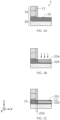
- the Figures 1A-1C present the steps of such a recrystallization process called SPER (acronym for “solid-phase epitaxial regrowth” in English terminology).
- the Figure 1A illustrates a device 1 intended to form a transistor and comprising a gate pattern 10 flanked by a spacer 11 on a substrate 20 of SOI type (acronym for “Silicon on Insulator” or “silicon on insulator” in French).
- the Figure 1B illustrates an ion bombardment at the edge of the spacer 11, adapted to partially amorphize the upper silicon layer 22 (topSi) of the SOI substrate, and to implant dopants in this amorphous part 22a.
- FIG. 1C illustrates the partial recrystallization of topSi from this 22b seed. During recrystallization, the dopants are incorporated and activated. This recrystallization ultimately allows a 13-doped zone to be obtained.
- a disadvantage of this solution based on the SPER recrystallization process is that there is an undoped area 22d between channel 15 and doped area 13, under spacer 11. This increases the access resistance of the transistor. Another disadvantage is the presence of the undoped seed 22b underlying the doped area 13. This further increases the access resistance of the transistor.
- good control of the amorphization depth becomes essential. The implementation of the SPER process is therefore complex.
- the recrystallization of the amorphous part 22a of the topSi is generally not complete. A residual superficial uncrystallized layer 22c remains, it is then necessary to provide an etching to eliminate it.
- An object of the present invention is to at least partially overcome some of the drawbacks mentioned above.
- an object of the present invention is to provide a method of forming a doped area improving the access resistance of a microelectronic device.
- the removal of the first portion of the active layer is carried out before the formation of the first spacer. This allows the first portion to be removed at the earliest near the gate pattern.
- the edge of the second portion extends substantially as an extension of the lateral flank.
- the formation of the doped region is done from this edge. This edge thus becomes a junction between the second portion, typically the transistor channel, and the doped region, typically the source or drain of the transistor. This junction is preferably abrupt.
- the formation of the doped zone by lateral epitaxy, i.e. from the edge of the second portion, also makes it possible to avoid the need to keep an epitaxy seed underlying a modified portion, as implemented by known methods.
- the removal of the first portion can be carried out over the entire thickness of the active layer, up to the insulating layer, so that the doped zone has a thickness at least equal to that of the active layer, under the first and second spacers. It is therefore not necessary to precisely control an implantation depth, unlike known methods. This simplifies the process.
- a doped zone extending along the entire height of the active layer also makes it possible to reduce the access resistance of the transistor.
- Such a process can advantageously be implemented at low temperature, typically for temperatures T ⁇ 600°C. This process is thus compatible with 3D integration technology.
- the base portion of the first spacer has a thickness in the z direction substantially equal to the thickness of the active layer.
- a base portion of the first spacer having a thickness less than the thickness of the active layer does not allow the access resistance of the transistor to be optimally reduced.
- a base portion of the first spacer having a thickness greater than the thickness of the active layer does not allow the gate of the transistor to be correctly insulated.
- a base portion of the first spacer having a thickness substantially equal to the thickness of the active layer makes it possible to reduce the access resistance of the transistor in an optimized manner.
- a base portion thickness “substantially equal” to the thickness of the active layer means that the base portion thickness is equal to the thickness of the active layer at ⁇ 10%, preferably at ⁇ 5%.
- the selectivity of the selective etching of the first material with respect to the semiconductor material is greater than or equal to 10:1, and preferably greater than or equal to 20:1.
- the selectivity of the selective etching of the first material with respect to the second material is greater than or equal to 5:1, and preferably greater than or equal to 10:1.
- forming the first spacer includes depositing a first non-conformal layer such that the first layer has a thickness e y on the sidewall and a thickness e z on the insulating layer, such that the thickness e y is less than the thickness e z .
- a first spacer formed from a first non-conformal layer provides a thicker basal spacer portion than the sidewall spacer portion, preferably such that the basal spacer portion has a thickness substantially equal to the thickness of the active layer.
- a thinner sidewall spacer portion provides for finer and easier control of the “critical dimension” known by the acronym CD (“critical dimension”: this is the dimension on which the dimensional control of transistors is based).
- the first material and the second material are dielectric materials.
- the removal of the first portion is performed by anisotropic dry etching along the z direction.
- the epitaxy of the doped zone is a lateral epitaxy mainly directed in a direction normal to the edge of the second portion.
- the transistor gate pattern serves as an etch mask when removing the first portion.
- the epitaxy of the doped area is implemented with in situ doping so that the doped area directly exhibits doping at the end of said epitaxy.
- the term “on”, “overcomes”, “covers” or “underlying” or their equivalents do not necessarily mean “in contact with”.
- the deposition of a first layer on a second layer does not necessarily mean that the two layers are directly in contact with each other, but it does mean that the first layer at least partially covers the second layer by being either directly in contact with it or by being separated from it by at least one other layer or at least one other element.
- a layer can also be composed of several sub-layers of the same material or of different materials.
- a substrate, a layer, a device, “based” on a material M means a substrate, a layer, a device comprising this material M only or this material M and possibly other materials, for example alloying elements, impurities or doping elements.
- a silicon nitride SiN spacer may, for example, comprise non-stoichiometric silicon nitride (SiN), or stoichiometric silicon nitride (Si3N4), or even a silicon oxynitride (SiON).
- a spacer forms a ring around the grid, with a closed contour; the description of a spacer is preferably understood to mean this single spacer around the grid; however, the sectional illustration drawings, generally along a plane transverse to the longitudinal direction of the grids, show two spacer parts on either side of the sides of the grid. By extension, these two spacer parts are often referred to as “the spacers”. This latter terminology may optionally be adopted in this application, in this case “the first spacers” and/or “the second spacers”. Furthermore, the invention extends to embodiments in which “the first spacers” and/or “the second spacers” are discontinuous.
- the present invention allows in particular the fabrication of at least one transistor or a plurality of transistors on a substrate.
- This substrate may be of the semiconductor on insulator type, for example a silicon on insulator SOI substrate (acronym for "silicon on insulator”) or a germanium on insulator GeOl substrate (acronym for "germanium on insulator”).
- the invention can also be implemented more broadly for different microelectronic devices or components.
- a microelectronic component, device or element is any type of element made using microelectronics. These devices include, in addition to devices for purely electronic purposes, micromechanical or electromechanical devices (MEMS, NEMS, etc.) as well as optical or optoelectronic devices (MOEMS, etc.).
- MEMS micromechanical or electromechanical devices
- MOEMS optical or optoelectronic devices
- successive steps of the manufacturing method are described below.
- the adjective “successive” does not necessarily imply, even if this is generally preferred, that the steps follow one another immediately, intermediate steps being able to separate them.
- the term “step” means the carrying out of a part of the method, and can designate a set of sub-steps.
- dielectric describes a material whose electrical conductivity is sufficiently low in the given application to serve as an insulator.
- a dielectric material preferably has a dielectric constant of less than 7. Spacers are typically formed from a dielectric material.
- Selective etching with respect to or “etching exhibiting selectivity with respect to” means etching configured to remove a material A or a layer A with respect to a material B or a layer B, and exhibiting an etching rate of the material A greater than the etching rate of the material B.
- Selectivity is the ratio of the etching rate of the material A to the etching rate of the material B.
- thickness for a layer height for a device (transistor or gate for example) and depth for a cavity or an etching.
- the thickness is taken in a direction normal to the main extension plane of the layer, the height and depth are taken in a direction normal to the base plane of the substrate.
- the main extension plane of the layer, respectively the base plane of the substrate is generally parallel to a lower face or an upper face of this layer, respectively of this substrate.
- a preferably orthonormal reference frame formed by the x, y, z axes is shown in the accompanying drawings.
- the substrate more precisely its lower face and/or its upper face, extends in the xy basal plane.
Landscapes
- Thin Film Transistor (AREA)
- Insulated Gate Type Field-Effect Transistor (AREA)
Claims (12)
- Verfahren zur Bildung mindestens eines dotierten Bereichs (13) zur Bildung einer Quelle oder eines Drains eines Transistors (1), umfassend die folgenden Schritte:• Bereitstellen eines Stapels, der in einer z-Richtung mindestens eine Isolierschicht (21), eine aktive Schicht (22) aus einem Halbleitermaterial umfasst, die die Isolierschicht (21) überlagert, und ein Transistor-Gittermuster (10), das die aktive Schicht (22) überlagert und mindestens eine Seitenflanke (100) aufweist, die sich in einer Ebene im Wesentlichen senkrecht zu einer Oberseite (220) der aktiven Schicht (22) erstreckt,• Entfernen eines ersten Abschnitts (221) der aktiven Schicht (22), der nicht vom Gittermuster (10) überlagert wird, wobei sich der erste Abschnitt (221) bis zur Senkrechten des Gittermusters (10) erstreckt, direkt am Rand eines zweiten Abschnitts (222, 15) der aktiven Schicht (22), wobei der zweite Abschnitt (222, 15) sich unter dem Gittermuster (10) befindet, so dass eine Kante (150) des zweiten Abschnitts (222, 15) freigelegt wird, wobei sich die Kante (150) in einer Verlängerung der Seitenflanke (100) des Gittermusters (10) erstreckt,• Bilden eines ersten Abstandshalters (11) aus einem ersten Material an der Seitenflanke (100) und an der Kante (150), wobei der erste Abstandshalter (11) eine L-Form aufweist und einen Basalabschnitt (11b) in Kontakt mit der Isolierschicht (21) und einen Seitenabschnitt (111) in Kontakt mit der Seitenflanke (100) umfasst, wobei der Basalabschnitt (11b) eine Dicke in der z-Richtung aufweist, die im Wesentlichen gleich der Dicke der aktiven Schicht (22) ist,• Bilden eines zweiten Abstandshalters (12) aus einem zweiten Material auf dem ersten Abstandshalter (11), wobei der zweite Abstandshalter (12) eine Form aufweist, die der des ersten Abstandshalters (11) entspricht,• Entfernen des Basalabschnitts (11b) des ersten Abstandshalters (11) durch selektives Ätzen des ersten Materials gegenüber dem zweiten Material des zweiten Abstandshalters (12) und dem Halbleitermaterial, so dass die Kante (150) des zweiten Abschnitts (222, 15) freigelegt wird, wobei der Seitenabschnitt (111) des ersten Abstandshalters (11) mindestens teilweise an der Seitenflanke (100) des Gittermusters (10) erhalten bleibt,• Bilden durch Epitaxie ausgehend von der freiliegenden Kante (150) des dotierten Bereichs (13).
- Verfahren nach dem vorhergehenden Anspruch, wobei die Selektivität des selektiven Ätzens des ersten Materials gegenüber dem Halbleitermaterial größer oder gleich 10:1 und vorzugsweise größer oder gleich 20:1 ist.
- Verfahren nach einem der vorhergehenden Ansprüche, wobei die Selektivität des selektiven Ätzens des ersten Materials gegenüber dem zweiten Material größer oder gleich 5:1 und vorzugsweise größer oder gleich 10:1 ist.
- Verfahren nach einem der vorhergehenden Ansprüche, wobei die Bildung des ersten Abstandhalters (11) die Ablagerung einer nicht konformen ersten Schicht (110) umfasst, so dass die erste Schicht (110) eine Dicke ey an der Seitenflanke (100) und eine Dicke ez an der Isolierschicht (21) aufweist, so dass die Dicke ey kleiner als die Dicke ez ist.
- Verfahren nach einem der vorhergehenden Ansprüche, wobei das Halbleitermaterial der aktiven Schicht (22) aus Silizium und Siliziumgermanium entnommen wird und wobei der dotierte Bereich (13) auf Silizium- oder Siliziumgermaniumbasis beruht.
- Verfahren nach einem der vorhergehenden Ansprüche, wobei das erste Material und das zweite Material dielektrische Materialien sind.
- Verfahren nach einem der vorhergehenden Ansprüche, wobei das erste Material auf Siliziumoxid- oder SiBCN-Basis beruht, und wobei das zweite Material sich vom ersten Material unterscheidet und auf Siliziumnitrid-SiN- oder SiCO-Basis oder einem anderen Material beruht, das mindestens zwei Arten von Si, C, O, B, N umfasst.
- Verfahren nach einem der vorhergehenden Ansprüche, wobei die Epitaxie des dotierten Bereichs so eingerichtet ist, dass sich der dotierte Bereich (13) über die Oberseite (220) der aktiven Schicht (22) in einer Richtung im Wesentlichen senkrecht zur aktiven Schicht (22) erstreckt.
- Verfahren nach einem der vorhergehenden Ansprüche, wobei das Entfernen des ersten Abschnitts (221) durch anisotropes Trockenätzen in z-Richtung erfolgt.
- Verfahren nach einem der vorhergehenden Ansprüche, wobei die Epitaxie des dotierten Bereichs (13) eine laterale Epitaxie ist, die nur aus der Kante (150) des zweiten Abschnitts (222, 15) hervorgeht.
- Verfahren nach einem der vorhergehenden Ansprüche, wobei das Transistor-Gittermuster (10) beim Entfernen des ersten Abschnitts (221) als Graviermaske dient.
- Verfahren nach einem der vorhergehenden Ansprüche, wobei die Epitaxie des dotierten Bereichs (13) mit einer In-situ-Dotierung durchgeführt wird, so dass der dotierte Bereich (13) nach der Epitaxie direkt dotiert wird.
Applications Claiming Priority (1)
| Application Number | Priority Date | Filing Date | Title |
|---|---|---|---|
| FR2011824A FR3116380B1 (fr) | 2020-11-18 | 2020-11-18 | Procédé de fabrication d’une zone dopée d’un dispositif microélectronique |
Publications (2)
| Publication Number | Publication Date |
|---|---|
| EP4002482A1 EP4002482A1 (de) | 2022-05-25 |
| EP4002482B1 true EP4002482B1 (de) | 2025-05-07 |
Family
ID=74206029
Family Applications (1)
| Application Number | Title | Priority Date | Filing Date |
|---|---|---|---|
| EP21208504.7A Active EP4002482B1 (de) | 2020-11-18 | 2021-11-16 | Verfahren zur herstellung eines bereichs, der mit einer mikroelektronischen vorrichtung dotiert ist |
Country Status (3)
| Country | Link |
|---|---|
| US (1) | US11967633B2 (de) |
| EP (1) | EP4002482B1 (de) |
| FR (1) | FR3116380B1 (de) |
Family Cites Families (6)
| Publication number | Priority date | Publication date | Assignee | Title |
|---|---|---|---|---|
| US6232641B1 (en) | 1998-05-29 | 2001-05-15 | Kabushiki Kaisha Toshiba | Semiconductor apparatus having elevated source and drain structure and manufacturing method therefor |
| US7473947B2 (en) | 2002-07-12 | 2009-01-06 | Intel Corporation | Process for ultra-thin body SOI devices that incorporate EPI silicon tips and article made thereby |
| KR100498475B1 (ko) | 2003-01-07 | 2005-07-01 | 삼성전자주식회사 | 모스 전계 효과 트랜지스터 구조 및 그 제조 방법 |
| FR3002080B1 (fr) | 2013-02-11 | 2015-03-27 | Commissariat Energie Atomique | Procede de fabrication d'un transistor |
| FR3009651B1 (fr) * | 2013-08-09 | 2016-12-23 | Commissariat Energie Atomique | Procede ameliore de realisation de zones dopees et/ou exercant une contrainte sous les espaceurs d'un transistor |
| FR3034909B1 (fr) * | 2015-04-09 | 2018-02-23 | Commissariat A L'energie Atomique Et Aux Energies Alternatives | Procede de dopage des regions de source et de drain d'un transistor a l'aide d'une amorphisation selective |
-
2020
- 2020-11-18 FR FR2011824A patent/FR3116380B1/fr active Active
-
2021
- 2021-11-16 EP EP21208504.7A patent/EP4002482B1/de active Active
- 2021-11-18 US US17/455,425 patent/US11967633B2/en active Active
Also Published As
| Publication number | Publication date |
|---|---|
| FR3116380A1 (fr) | 2022-05-20 |
| EP4002482A1 (de) | 2022-05-25 |
| US11967633B2 (en) | 2024-04-23 |
| US20220157970A1 (en) | 2022-05-19 |
| FR3116380B1 (fr) | 2022-12-16 |
Similar Documents
| Publication | Publication Date | Title |
|---|---|---|
| EP2876677B1 (de) | Verfahren zur Bildung von Abstandhaltern eines Gates eines Transistors | |
| EP2999001B1 (de) | Einbringung von abstandhaltern an den seiten eines transistor-gates | |
| EP1091417A1 (de) | Herstellungsverfahren für Halbleiterbauelement mit Rundherum-Gate und dadurch hergestelltes Bauelement | |
| FR3060840A1 (fr) | Procede de realisation d'un dispositif semi-conducteur a espaceurs internes auto-alignes | |
| EP3261124B1 (de) | Verfahren zur bildung von abstandhaltern eines gates eines transistors | |
| WO2014037410A1 (fr) | Procédé de gravure d'un matériau semiconducteur cristallin par implantation ionique puis gravure chimique à base de chlorure d'hydrogène | |
| EP2610915A1 (de) | Transistor und Herstellungsverfahren eines Transistors | |
| FR3080486A1 (fr) | Procede de formation d'un dispositif microelectronique | |
| EP3506336B1 (de) | Ätzverfahren einer dielektrischen 3d-schicht | |
| EP3246948B1 (de) | Verfahren zur herstellung von transistoren, die unterschiedliche eigenschaften aufweisen, auf demselben substrat | |
| FR3047352A1 (fr) | Procede de fabrication d'un transistor a dopant localise a l'aplomb de la grille | |
| WO2014037411A1 (fr) | Procédé de réalisation de transistors fet | |
| EP3783644B1 (de) | Verfahren zur herstellung von mikroelektronischen komponenten | |
| EP4002482B1 (de) | Verfahren zur herstellung eines bereichs, der mit einer mikroelektronischen vorrichtung dotiert ist | |
| EP4006996B1 (de) | Quantenvorrichtung und ihr herstellungsverfahren | |
| FR3091002A1 (fr) | Procédé de gravure d’une couche diélectrique tridimensionnelle | |
| EP3961689A1 (de) | Verfahren zur herstellung von mikroelektronischen komponenten | |
| FR3098981A1 (fr) | procédé de fabrication de transistors | |
| EP4002486A1 (de) | Verfahren zur herstellung eines mit einer mikroelektronischen vorrichtung dotierten bereichs | |
| FR3046875A1 (fr) | Procede de fabrication d'un transistor | |
| EP3764393A1 (de) | Verfahren zur bildung von gräben | |
| EP4391082B1 (de) | Verfahren zur herstellung einer halbleiteranordnung mit einem rückgitter | |
| EP3968388B1 (de) | Verfahren zur herstellung eines mit einer mikroelektronischen vorrichtung dotierten bereichs | |
| FR3100085A1 (fr) | procédé de fabrication de composants micro-électroniques | |
| FR3046876A1 (fr) | Consommation du canal d'un transistor par oxydation sacrificielle |
Legal Events
| Date | Code | Title | Description |
|---|---|---|---|
| PUAI | Public reference made under article 153(3) epc to a published international application that has entered the european phase |
Free format text: ORIGINAL CODE: 0009012 |
|
| STAA | Information on the status of an ep patent application or granted ep patent |
Free format text: STATUS: REQUEST FOR EXAMINATION WAS MADE |
|
| 17P | Request for examination filed |
Effective date: 20211116 |
|
| AK | Designated contracting states |
Kind code of ref document: A1 Designated state(s): AL AT BE BG CH CY CZ DE DK EE ES FI FR GB GR HR HU IE IS IT LI LT LU LV MC MK MT NL NO PL PT RO RS SE SI SK SM TR |
|
| RAP3 | Party data changed (applicant data changed or rights of an application transferred) |
Owner name: COMMISSARIAT A L'ENERGIE ATOMIQUE ET AUX ENERGIESALTERNATIVES |
|
| GRAP | Despatch of communication of intention to grant a patent |
Free format text: ORIGINAL CODE: EPIDOSNIGR1 |
|
| STAA | Information on the status of an ep patent application or granted ep patent |
Free format text: STATUS: GRANT OF PATENT IS INTENDED |
|
| RIC1 | Information provided on ipc code assigned before grant |
Ipc: H01L 29/78 20060101ALI20241121BHEP Ipc: H01L 29/66 20060101AFI20241121BHEP |
|
| INTG | Intention to grant announced |
Effective date: 20241211 |
|
| GRAS | Grant fee paid |
Free format text: ORIGINAL CODE: EPIDOSNIGR3 |
|
| GRAA | (expected) grant |
Free format text: ORIGINAL CODE: 0009210 |
|
| STAA | Information on the status of an ep patent application or granted ep patent |
Free format text: STATUS: THE PATENT HAS BEEN GRANTED |
|
| AK | Designated contracting states |
Kind code of ref document: B1 Designated state(s): AL AT BE BG CH CY CZ DE DK EE ES FI FR GB GR HR HU IE IS IT LI LT LU LV MC MK MT NL NO PL PT RO RS SE SI SK SM TR |
|
| REG | Reference to a national code |
Ref country code: GB Ref legal event code: FG4D Free format text: NOT ENGLISH |
|
| REG | Reference to a national code |
Ref country code: DE Ref legal event code: R096 Ref document number: 602021030335 Country of ref document: DE |
|
| REG | Reference to a national code |
Ref country code: IE Ref legal event code: FG4D Free format text: LANGUAGE OF EP DOCUMENT: FRENCH |
|
| REG | Reference to a national code |
Ref country code: NL Ref legal event code: MP Effective date: 20250507 |
|
| PG25 | Lapsed in a contracting state [announced via postgrant information from national office to epo] |
Ref country code: PT Free format text: LAPSE BECAUSE OF FAILURE TO SUBMIT A TRANSLATION OF THE DESCRIPTION OR TO PAY THE FEE WITHIN THE PRESCRIBED TIME-LIMIT Effective date: 20250908 Ref country code: FI Free format text: LAPSE BECAUSE OF FAILURE TO SUBMIT A TRANSLATION OF THE DESCRIPTION OR TO PAY THE FEE WITHIN THE PRESCRIBED TIME-LIMIT Effective date: 20250507 Ref country code: ES Free format text: LAPSE BECAUSE OF FAILURE TO SUBMIT A TRANSLATION OF THE DESCRIPTION OR TO PAY THE FEE WITHIN THE PRESCRIBED TIME-LIMIT Effective date: 20250507 |
|
| REG | Reference to a national code |
Ref country code: LT Ref legal event code: MG9D |
|
| PG25 | Lapsed in a contracting state [announced via postgrant information from national office to epo] |
Ref country code: GR Free format text: LAPSE BECAUSE OF FAILURE TO SUBMIT A TRANSLATION OF THE DESCRIPTION OR TO PAY THE FEE WITHIN THE PRESCRIBED TIME-LIMIT Effective date: 20250808 Ref country code: NO Free format text: LAPSE BECAUSE OF FAILURE TO SUBMIT A TRANSLATION OF THE DESCRIPTION OR TO PAY THE FEE WITHIN THE PRESCRIBED TIME-LIMIT Effective date: 20250807 |
|
| PG25 | Lapsed in a contracting state [announced via postgrant information from national office to epo] |
Ref country code: NL Free format text: LAPSE BECAUSE OF FAILURE TO SUBMIT A TRANSLATION OF THE DESCRIPTION OR TO PAY THE FEE WITHIN THE PRESCRIBED TIME-LIMIT Effective date: 20250507 Ref country code: PL Free format text: LAPSE BECAUSE OF FAILURE TO SUBMIT A TRANSLATION OF THE DESCRIPTION OR TO PAY THE FEE WITHIN THE PRESCRIBED TIME-LIMIT Effective date: 20250507 |
|
| REG | Reference to a national code |
Ref country code: AT Ref legal event code: MK05 Ref document number: 1793482 Country of ref document: AT Kind code of ref document: T Effective date: 20250507 |
|
| PG25 | Lapsed in a contracting state [announced via postgrant information from national office to epo] |
Ref country code: BG Free format text: LAPSE BECAUSE OF FAILURE TO SUBMIT A TRANSLATION OF THE DESCRIPTION OR TO PAY THE FEE WITHIN THE PRESCRIBED TIME-LIMIT Effective date: 20250507 |
|
| PG25 | Lapsed in a contracting state [announced via postgrant information from national office to epo] |
Ref country code: HR Free format text: LAPSE BECAUSE OF FAILURE TO SUBMIT A TRANSLATION OF THE DESCRIPTION OR TO PAY THE FEE WITHIN THE PRESCRIBED TIME-LIMIT Effective date: 20250507 |
|
| PG25 | Lapsed in a contracting state [announced via postgrant information from national office to epo] |
Ref country code: AT Free format text: LAPSE BECAUSE OF FAILURE TO SUBMIT A TRANSLATION OF THE DESCRIPTION OR TO PAY THE FEE WITHIN THE PRESCRIBED TIME-LIMIT Effective date: 20250507 |
|
| PG25 | Lapsed in a contracting state [announced via postgrant information from national office to epo] |
Ref country code: RS Free format text: LAPSE BECAUSE OF FAILURE TO SUBMIT A TRANSLATION OF THE DESCRIPTION OR TO PAY THE FEE WITHIN THE PRESCRIBED TIME-LIMIT Effective date: 20250807 |
|
| PG25 | Lapsed in a contracting state [announced via postgrant information from national office to epo] |
Ref country code: IS Free format text: LAPSE BECAUSE OF FAILURE TO SUBMIT A TRANSLATION OF THE DESCRIPTION OR TO PAY THE FEE WITHIN THE PRESCRIBED TIME-LIMIT Effective date: 20250907 |
|
| PG25 | Lapsed in a contracting state [announced via postgrant information from national office to epo] |
Ref country code: LV Free format text: LAPSE BECAUSE OF FAILURE TO SUBMIT A TRANSLATION OF THE DESCRIPTION OR TO PAY THE FEE WITHIN THE PRESCRIBED TIME-LIMIT Effective date: 20250507 |
|
| PGFP | Annual fee paid to national office [announced via postgrant information from national office to epo] |
Ref country code: DE Payment date: 20251118 Year of fee payment: 5 |
|
| PGFP | Annual fee paid to national office [announced via postgrant information from national office to epo] |
Ref country code: GB Payment date: 20251125 Year of fee payment: 5 |
|
| PG25 | Lapsed in a contracting state [announced via postgrant information from national office to epo] |
Ref country code: DK Free format text: LAPSE BECAUSE OF FAILURE TO SUBMIT A TRANSLATION OF THE DESCRIPTION OR TO PAY THE FEE WITHIN THE PRESCRIBED TIME-LIMIT Effective date: 20250507 Ref country code: SM Free format text: LAPSE BECAUSE OF FAILURE TO SUBMIT A TRANSLATION OF THE DESCRIPTION OR TO PAY THE FEE WITHIN THE PRESCRIBED TIME-LIMIT Effective date: 20250507 |
|
| PGFP | Annual fee paid to national office [announced via postgrant information from national office to epo] |
Ref country code: FR Payment date: 20251125 Year of fee payment: 5 |
|
| PG25 | Lapsed in a contracting state [announced via postgrant information from national office to epo] |
Ref country code: CZ Free format text: LAPSE BECAUSE OF FAILURE TO SUBMIT A TRANSLATION OF THE DESCRIPTION OR TO PAY THE FEE WITHIN THE PRESCRIBED TIME-LIMIT Effective date: 20250507 |
|
| PG25 | Lapsed in a contracting state [announced via postgrant information from national office to epo] |
Ref country code: EE Free format text: LAPSE BECAUSE OF FAILURE TO SUBMIT A TRANSLATION OF THE DESCRIPTION OR TO PAY THE FEE WITHIN THE PRESCRIBED TIME-LIMIT Effective date: 20250507 |
|
| PG25 | Lapsed in a contracting state [announced via postgrant information from national office to epo] |
Ref country code: RO Free format text: LAPSE BECAUSE OF FAILURE TO SUBMIT A TRANSLATION OF THE DESCRIPTION OR TO PAY THE FEE WITHIN THE PRESCRIBED TIME-LIMIT Effective date: 20250507 Ref country code: SK Free format text: LAPSE BECAUSE OF FAILURE TO SUBMIT A TRANSLATION OF THE DESCRIPTION OR TO PAY THE FEE WITHIN THE PRESCRIBED TIME-LIMIT Effective date: 20250507 |
|
| PG25 | Lapsed in a contracting state [announced via postgrant information from national office to epo] |
Ref country code: IT Free format text: LAPSE BECAUSE OF FAILURE TO SUBMIT A TRANSLATION OF THE DESCRIPTION OR TO PAY THE FEE WITHIN THE PRESCRIBED TIME-LIMIT Effective date: 20250507 |
|
| REG | Reference to a national code |
Ref country code: DE Ref legal event code: R097 Ref document number: 602021030335 Country of ref document: DE |
|
| PLBE | No opposition filed within time limit |
Free format text: ORIGINAL CODE: 0009261 |
|
| STAA | Information on the status of an ep patent application or granted ep patent |
Free format text: STATUS: NO OPPOSITION FILED WITHIN TIME LIMIT |
|
| REG | Reference to a national code |
Ref country code: CH Ref legal event code: L10 Free format text: ST27 STATUS EVENT CODE: U-0-0-L10-L00 (AS PROVIDED BY THE NATIONAL OFFICE) Effective date: 20260318 |
|
| 26N | No opposition filed |
Effective date: 20260210 |