EP3000904A2 - Feuille de cuivre avec support, procédé de production associé, feuille de cuivre avec support pour carte de circuit imprimé et une telle carte - Google Patents
Feuille de cuivre avec support, procédé de production associé, feuille de cuivre avec support pour carte de circuit imprimé et une telle carte Download PDFInfo
- Publication number
- EP3000904A2 EP3000904A2 EP15170556.3A EP15170556A EP3000904A2 EP 3000904 A2 EP3000904 A2 EP 3000904A2 EP 15170556 A EP15170556 A EP 15170556A EP 3000904 A2 EP3000904 A2 EP 3000904A2
- Authority
- EP
- European Patent Office
- Prior art keywords
- layer
- copper foil
- carrier
- resin
- copper
- Prior art date
- Legal status (The legal status is an assumption and is not a legal conclusion. Google has not performed a legal analysis and makes no representation as to the accuracy of the status listed.)
- Ceased
Links
Images
Classifications
-
- H—ELECTRICITY
- H05—ELECTRIC TECHNIQUES NOT OTHERWISE PROVIDED FOR
- H05K—PRINTED CIRCUITS; CASINGS OR CONSTRUCTIONAL DETAILS OF ELECTRIC APPARATUS; MANUFACTURE OF ASSEMBLAGES OF ELECTRICAL COMPONENTS
- H05K1/00—Printed circuits
- H05K1/02—Details
- H05K1/09—Use of materials for the conductive, e.g. metallic pattern
-
- B—PERFORMING OPERATIONS; TRANSPORTING
- B32—LAYERED PRODUCTS
- B32B—LAYERED PRODUCTS, i.e. PRODUCTS BUILT-UP OF STRATA OF FLAT OR NON-FLAT, e.g. CELLULAR OR HONEYCOMB, FORM
- B32B15/00—Layered products comprising a layer of metal
- B32B15/01—Layered products comprising a layer of metal all layers being exclusively metallic
- B32B15/013—Layered products comprising a layer of metal all layers being exclusively metallic one layer being formed of an iron alloy or steel, another layer being formed of a metal other than iron or aluminium
- B32B15/015—Layered products comprising a layer of metal all layers being exclusively metallic one layer being formed of an iron alloy or steel, another layer being formed of a metal other than iron or aluminium the said other metal being copper or nickel or an alloy thereof
-
- B—PERFORMING OPERATIONS; TRANSPORTING
- B32—LAYERED PRODUCTS
- B32B—LAYERED PRODUCTS, i.e. PRODUCTS BUILT-UP OF STRATA OF FLAT OR NON-FLAT, e.g. CELLULAR OR HONEYCOMB, FORM
- B32B15/00—Layered products comprising a layer of metal
- B32B15/04—Layered products comprising a layer of metal comprising metal as the main or only constituent of a layer, which is next to another layer of the same or of a different material
- B32B15/08—Layered products comprising a layer of metal comprising metal as the main or only constituent of a layer, which is next to another layer of the same or of a different material of synthetic resin
-
- B—PERFORMING OPERATIONS; TRANSPORTING
- B32—LAYERED PRODUCTS
- B32B—LAYERED PRODUCTS, i.e. PRODUCTS BUILT-UP OF STRATA OF FLAT OR NON-FLAT, e.g. CELLULAR OR HONEYCOMB, FORM
- B32B15/00—Layered products comprising a layer of metal
- B32B15/20—Layered products comprising a layer of metal comprising aluminium or copper
-
- B—PERFORMING OPERATIONS; TRANSPORTING
- B32—LAYERED PRODUCTS
- B32B—LAYERED PRODUCTS, i.e. PRODUCTS BUILT-UP OF STRATA OF FLAT OR NON-FLAT, e.g. CELLULAR OR HONEYCOMB, FORM
- B32B3/00—Layered products comprising a layer with external or internal discontinuities or unevennesses, or a layer of non-planar shape; Layered products comprising a layer having particular features of form
- B32B3/26—Layered products comprising a layer with external or internal discontinuities or unevennesses, or a layer of non-planar shape; Layered products comprising a layer having particular features of form characterised by a particular shape of the outline of the cross-section of a continuous layer; characterised by a layer with cavities or internal voids ; characterised by an apertured layer
- B32B3/30—Layered products comprising a layer with external or internal discontinuities or unevennesses, or a layer of non-planar shape; Layered products comprising a layer having particular features of form characterised by a particular shape of the outline of the cross-section of a continuous layer; characterised by a layer with cavities or internal voids ; characterised by an apertured layer characterised by a layer formed with recesses or projections, e.g. hollows, grooves, protuberances, ribs
-
- B—PERFORMING OPERATIONS; TRANSPORTING
- B32—LAYERED PRODUCTS
- B32B—LAYERED PRODUCTS, i.e. PRODUCTS BUILT-UP OF STRATA OF FLAT OR NON-FLAT, e.g. CELLULAR OR HONEYCOMB, FORM
- B32B9/00—Layered products comprising a layer of a particular substance not covered by groups B32B11/00 - B32B29/00
- B32B9/04—Layered products comprising a layer of a particular substance not covered by groups B32B11/00 - B32B29/00 comprising such particular substance as the main or only constituent of a layer, which is next to another layer of the same or of a different material
-
- C—CHEMISTRY; METALLURGY
- C22—METALLURGY; FERROUS OR NON-FERROUS ALLOYS; TREATMENT OF ALLOYS OR NON-FERROUS METALS
- C22C—ALLOYS
- C22C9/00—Alloys based on copper
-
- C—CHEMISTRY; METALLURGY
- C25—ELECTROLYTIC OR ELECTROPHORETIC PROCESSES; APPARATUS THEREFOR
- C25D—PROCESSES FOR THE ELECTROLYTIC OR ELECTROPHORETIC PRODUCTION OF COATINGS; ELECTROFORMING; APPARATUS THEREFOR
- C25D1/00—Electroforming
- C25D1/04—Wires; Strips; Foils
-
- C—CHEMISTRY; METALLURGY
- C25—ELECTROLYTIC OR ELECTROPHORETIC PROCESSES; APPARATUS THEREFOR
- C25D—PROCESSES FOR THE ELECTROLYTIC OR ELECTROPHORETIC PRODUCTION OF COATINGS; ELECTROFORMING; APPARATUS THEREFOR
- C25D5/00—Electroplating characterised by the process; Pretreatment or after-treatment of workpieces
- C25D5/10—Electroplating with more than one layer of the same or of different metals
- C25D5/12—Electroplating with more than one layer of the same or of different metals at least one layer being of nickel or chromium
-
- H—ELECTRICITY
- H05—ELECTRIC TECHNIQUES NOT OTHERWISE PROVIDED FOR
- H05K—PRINTED CIRCUITS; CASINGS OR CONSTRUCTIONAL DETAILS OF ELECTRIC APPARATUS; MANUFACTURE OF ASSEMBLAGES OF ELECTRICAL COMPONENTS
- H05K1/00—Printed circuits
- H05K1/02—Details
- H05K1/03—Use of materials for the substrate
- H05K1/0313—Organic insulating material
-
- H—ELECTRICITY
- H05—ELECTRIC TECHNIQUES NOT OTHERWISE PROVIDED FOR
- H05K—PRINTED CIRCUITS; CASINGS OR CONSTRUCTIONAL DETAILS OF ELECTRIC APPARATUS; MANUFACTURE OF ASSEMBLAGES OF ELECTRICAL COMPONENTS
- H05K3/00—Apparatus or processes for manufacturing printed circuits
- H05K3/02—Apparatus or processes for manufacturing printed circuits in which the conductive material is applied to the surface of the insulating support and is thereafter removed from such areas of the surface which are not intended for current conducting or shielding
- H05K3/022—Processes for manufacturing precursors of printed circuits, i.e. copper-clad substrates
- H05K3/025—Processes for manufacturing precursors of printed circuits, i.e. copper-clad substrates by transfer of thin metal foil formed on a temporary carrier, e.g. peel-apart copper
-
- H—ELECTRICITY
- H05—ELECTRIC TECHNIQUES NOT OTHERWISE PROVIDED FOR
- H05K—PRINTED CIRCUITS; CASINGS OR CONSTRUCTIONAL DETAILS OF ELECTRIC APPARATUS; MANUFACTURE OF ASSEMBLAGES OF ELECTRICAL COMPONENTS
- H05K3/00—Apparatus or processes for manufacturing printed circuits
- H05K3/02—Apparatus or processes for manufacturing printed circuits in which the conductive material is applied to the surface of the insulating support and is thereafter removed from such areas of the surface which are not intended for current conducting or shielding
- H05K3/06—Apparatus or processes for manufacturing printed circuits in which the conductive material is applied to the surface of the insulating support and is thereafter removed from such areas of the surface which are not intended for current conducting or shielding the conductive material being removed chemically or electrolytically, e.g. by photo-etch process
-
- H—ELECTRICITY
- H05—ELECTRIC TECHNIQUES NOT OTHERWISE PROVIDED FOR
- H05K—PRINTED CIRCUITS; CASINGS OR CONSTRUCTIONAL DETAILS OF ELECTRIC APPARATUS; MANUFACTURE OF ASSEMBLAGES OF ELECTRICAL COMPONENTS
- H05K3/00—Apparatus or processes for manufacturing printed circuits
- H05K3/10—Apparatus or processes for manufacturing printed circuits in which conductive material is applied to the insulating support in such a manner as to form the desired conductive pattern
- H05K3/18—Apparatus or processes for manufacturing printed circuits in which conductive material is applied to the insulating support in such a manner as to form the desired conductive pattern using precipitation techniques to apply the conductive material
- H05K3/181—Apparatus or processes for manufacturing printed circuits in which conductive material is applied to the insulating support in such a manner as to form the desired conductive pattern using precipitation techniques to apply the conductive material by electroless plating
-
- H—ELECTRICITY
- H05—ELECTRIC TECHNIQUES NOT OTHERWISE PROVIDED FOR
- H05K—PRINTED CIRCUITS; CASINGS OR CONSTRUCTIONAL DETAILS OF ELECTRIC APPARATUS; MANUFACTURE OF ASSEMBLAGES OF ELECTRICAL COMPONENTS
- H05K3/00—Apparatus or processes for manufacturing printed circuits
- H05K3/10—Apparatus or processes for manufacturing printed circuits in which conductive material is applied to the insulating support in such a manner as to form the desired conductive pattern
- H05K3/18—Apparatus or processes for manufacturing printed circuits in which conductive material is applied to the insulating support in such a manner as to form the desired conductive pattern using precipitation techniques to apply the conductive material
- H05K3/188—Apparatus or processes for manufacturing printed circuits in which conductive material is applied to the insulating support in such a manner as to form the desired conductive pattern using precipitation techniques to apply the conductive material by direct electroplating
-
- H—ELECTRICITY
- H05—ELECTRIC TECHNIQUES NOT OTHERWISE PROVIDED FOR
- H05K—PRINTED CIRCUITS; CASINGS OR CONSTRUCTIONAL DETAILS OF ELECTRIC APPARATUS; MANUFACTURE OF ASSEMBLAGES OF ELECTRICAL COMPONENTS
- H05K3/00—Apparatus or processes for manufacturing printed circuits
- H05K3/22—Secondary treatment of printed circuits
- H05K3/24—Reinforcing of the conductive pattern
-
- H—ELECTRICITY
- H05—ELECTRIC TECHNIQUES NOT OTHERWISE PROVIDED FOR
- H05K—PRINTED CIRCUITS; CASINGS OR CONSTRUCTIONAL DETAILS OF ELECTRIC APPARATUS; MANUFACTURE OF ASSEMBLAGES OF ELECTRICAL COMPONENTS
- H05K3/00—Apparatus or processes for manufacturing printed circuits
- H05K3/38—Improvement of the adhesion between the insulating substrate and the metal
- H05K3/381—Improvement of the adhesion between the insulating substrate and the metal by special treatment of the substrate
-
- H—ELECTRICITY
- H05—ELECTRIC TECHNIQUES NOT OTHERWISE PROVIDED FOR
- H05K—PRINTED CIRCUITS; CASINGS OR CONSTRUCTIONAL DETAILS OF ELECTRIC APPARATUS; MANUFACTURE OF ASSEMBLAGES OF ELECTRICAL COMPONENTS
- H05K3/00—Apparatus or processes for manufacturing printed circuits
- H05K3/38—Improvement of the adhesion between the insulating substrate and the metal
- H05K3/382—Improvement of the adhesion between the insulating substrate and the metal by special treatment of the metal
- H05K3/383—Improvement of the adhesion between the insulating substrate and the metal by special treatment of the metal by microetching
-
- H—ELECTRICITY
- H05—ELECTRIC TECHNIQUES NOT OTHERWISE PROVIDED FOR
- H05K—PRINTED CIRCUITS; CASINGS OR CONSTRUCTIONAL DETAILS OF ELECTRIC APPARATUS; MANUFACTURE OF ASSEMBLAGES OF ELECTRICAL COMPONENTS
- H05K3/00—Apparatus or processes for manufacturing printed circuits
- H05K3/38—Improvement of the adhesion between the insulating substrate and the metal
- H05K3/382—Improvement of the adhesion between the insulating substrate and the metal by special treatment of the metal
- H05K3/384—Improvement of the adhesion between the insulating substrate and the metal by special treatment of the metal by plating
-
- H—ELECTRICITY
- H05—ELECTRIC TECHNIQUES NOT OTHERWISE PROVIDED FOR
- H05K—PRINTED CIRCUITS; CASINGS OR CONSTRUCTIONAL DETAILS OF ELECTRIC APPARATUS; MANUFACTURE OF ASSEMBLAGES OF ELECTRICAL COMPONENTS
- H05K3/00—Apparatus or processes for manufacturing printed circuits
- H05K3/38—Improvement of the adhesion between the insulating substrate and the metal
- H05K3/388—Improvement of the adhesion between the insulating substrate and the metal by the use of a metallic or inorganic thin film adhesion layer
-
- B—PERFORMING OPERATIONS; TRANSPORTING
- B32—LAYERED PRODUCTS
- B32B—LAYERED PRODUCTS, i.e. PRODUCTS BUILT-UP OF STRATA OF FLAT OR NON-FLAT, e.g. CELLULAR OR HONEYCOMB, FORM
- B32B2307/00—Properties of the layers or laminate
- B32B2307/30—Properties of the layers or laminate having particular thermal properties
- B32B2307/306—Resistant to heat
-
- B—PERFORMING OPERATIONS; TRANSPORTING
- B32—LAYERED PRODUCTS
- B32B—LAYERED PRODUCTS, i.e. PRODUCTS BUILT-UP OF STRATA OF FLAT OR NON-FLAT, e.g. CELLULAR OR HONEYCOMB, FORM
- B32B2307/00—Properties of the layers or laminate
- B32B2307/70—Other properties
- B32B2307/714—Inert, i.e. inert to chemical degradation, corrosion
-
- B—PERFORMING OPERATIONS; TRANSPORTING
- B32—LAYERED PRODUCTS
- B32B—LAYERED PRODUCTS, i.e. PRODUCTS BUILT-UP OF STRATA OF FLAT OR NON-FLAT, e.g. CELLULAR OR HONEYCOMB, FORM
- B32B2457/00—Electrical equipment
- B32B2457/08—PCBs, i.e. printed circuit boards
-
- C—CHEMISTRY; METALLURGY
- C25—ELECTROLYTIC OR ELECTROPHORETIC PROCESSES; APPARATUS THEREFOR
- C25D—PROCESSES FOR THE ELECTROLYTIC OR ELECTROPHORETIC PRODUCTION OF COATINGS; ELECTROFORMING; APPARATUS THEREFOR
- C25D3/00—Electroplating: Baths therefor
- C25D3/02—Electroplating: Baths therefor from solutions
- C25D3/12—Electroplating: Baths therefor from solutions of nickel or cobalt
-
- C—CHEMISTRY; METALLURGY
- C25—ELECTROLYTIC OR ELECTROPHORETIC PROCESSES; APPARATUS THEREFOR
- C25D—PROCESSES FOR THE ELECTROLYTIC OR ELECTROPHORETIC PRODUCTION OF COATINGS; ELECTROFORMING; APPARATUS THEREFOR
- C25D3/00—Electroplating: Baths therefor
- C25D3/02—Electroplating: Baths therefor from solutions
- C25D3/38—Electroplating: Baths therefor from solutions of copper
-
- C—CHEMISTRY; METALLURGY
- C25—ELECTROLYTIC OR ELECTROPHORETIC PROCESSES; APPARATUS THEREFOR
- C25D—PROCESSES FOR THE ELECTROLYTIC OR ELECTROPHORETIC PRODUCTION OF COATINGS; ELECTROFORMING; APPARATUS THEREFOR
- C25D9/00—Electrolytic coating other than with metals
- C25D9/04—Electrolytic coating other than with metals with inorganic materials
- C25D9/08—Electrolytic coating other than with metals with inorganic materials by cathodic processes
-
- H—ELECTRICITY
- H05—ELECTRIC TECHNIQUES NOT OTHERWISE PROVIDED FOR
- H05K—PRINTED CIRCUITS; CASINGS OR CONSTRUCTIONAL DETAILS OF ELECTRIC APPARATUS; MANUFACTURE OF ASSEMBLAGES OF ELECTRICAL COMPONENTS
- H05K2201/00—Indexing scheme relating to printed circuits covered by H05K1/00
- H05K2201/03—Conductive materials
- H05K2201/0332—Structure of the conductor
- H05K2201/0335—Layered conductors or foils
- H05K2201/0355—Metal foils
-
- H—ELECTRICITY
- H05—ELECTRIC TECHNIQUES NOT OTHERWISE PROVIDED FOR
- H05K—PRINTED CIRCUITS; CASINGS OR CONSTRUCTIONAL DETAILS OF ELECTRIC APPARATUS; MANUFACTURE OF ASSEMBLAGES OF ELECTRICAL COMPONENTS
- H05K2201/00—Indexing scheme relating to printed circuits covered by H05K1/00
- H05K2201/09—Shape and layout
- H05K2201/09009—Substrate related
-
- H—ELECTRICITY
- H05—ELECTRIC TECHNIQUES NOT OTHERWISE PROVIDED FOR
- H05K—PRINTED CIRCUITS; CASINGS OR CONSTRUCTIONAL DETAILS OF ELECTRIC APPARATUS; MANUFACTURE OF ASSEMBLAGES OF ELECTRICAL COMPONENTS
- H05K2203/00—Indexing scheme relating to apparatus or processes for manufacturing printed circuits covered by H05K3/00
- H05K2203/11—Treatments characterised by their effect, e.g. heating, cooling, roughening
-
- Y—GENERAL TAGGING OF NEW TECHNOLOGICAL DEVELOPMENTS; GENERAL TAGGING OF CROSS-SECTIONAL TECHNOLOGIES SPANNING OVER SEVERAL SECTIONS OF THE IPC; TECHNICAL SUBJECTS COVERED BY FORMER USPC CROSS-REFERENCE ART COLLECTIONS [XRACs] AND DIGESTS
- Y10—TECHNICAL SUBJECTS COVERED BY FORMER USPC
- Y10T—TECHNICAL SUBJECTS COVERED BY FORMER US CLASSIFICATION
- Y10T428/00—Stock material or miscellaneous articles
- Y10T428/12—All metal or with adjacent metals
- Y10T428/12493—Composite; i.e., plural, adjacent, spatially distinct metal components [e.g., layers, joint, etc.]
- Y10T428/12535—Composite; i.e., plural, adjacent, spatially distinct metal components [e.g., layers, joint, etc.] with additional, spatially distinct nonmetal component
- Y10T428/12542—More than one such component
- Y10T428/12549—Adjacent to each other
-
- Y—GENERAL TAGGING OF NEW TECHNOLOGICAL DEVELOPMENTS; GENERAL TAGGING OF CROSS-SECTIONAL TECHNOLOGIES SPANNING OVER SEVERAL SECTIONS OF THE IPC; TECHNICAL SUBJECTS COVERED BY FORMER USPC CROSS-REFERENCE ART COLLECTIONS [XRACs] AND DIGESTS
- Y10—TECHNICAL SUBJECTS COVERED BY FORMER USPC
- Y10T—TECHNICAL SUBJECTS COVERED BY FORMER US CLASSIFICATION
- Y10T428/00—Stock material or miscellaneous articles
- Y10T428/12—All metal or with adjacent metals
- Y10T428/12493—Composite; i.e., plural, adjacent, spatially distinct metal components [e.g., layers, joint, etc.]
- Y10T428/12535—Composite; i.e., plural, adjacent, spatially distinct metal components [e.g., layers, joint, etc.] with additional, spatially distinct nonmetal component
- Y10T428/12556—Organic component
- Y10T428/12569—Synthetic resin
-
- Y—GENERAL TAGGING OF NEW TECHNOLOGICAL DEVELOPMENTS; GENERAL TAGGING OF CROSS-SECTIONAL TECHNOLOGIES SPANNING OVER SEVERAL SECTIONS OF THE IPC; TECHNICAL SUBJECTS COVERED BY FORMER USPC CROSS-REFERENCE ART COLLECTIONS [XRACs] AND DIGESTS
- Y10—TECHNICAL SUBJECTS COVERED BY FORMER USPC
- Y10T—TECHNICAL SUBJECTS COVERED BY FORMER US CLASSIFICATION
- Y10T428/00—Stock material or miscellaneous articles
- Y10T428/12—All metal or with adjacent metals
- Y10T428/12493—Composite; i.e., plural, adjacent, spatially distinct metal components [e.g., layers, joint, etc.]
- Y10T428/12535—Composite; i.e., plural, adjacent, spatially distinct metal components [e.g., layers, joint, etc.] with additional, spatially distinct nonmetal component
- Y10T428/12611—Oxide-containing component
-
- Y—GENERAL TAGGING OF NEW TECHNOLOGICAL DEVELOPMENTS; GENERAL TAGGING OF CROSS-SECTIONAL TECHNOLOGIES SPANNING OVER SEVERAL SECTIONS OF THE IPC; TECHNICAL SUBJECTS COVERED BY FORMER USPC CROSS-REFERENCE ART COLLECTIONS [XRACs] AND DIGESTS
- Y10—TECHNICAL SUBJECTS COVERED BY FORMER USPC
- Y10T—TECHNICAL SUBJECTS COVERED BY FORMER US CLASSIFICATION
- Y10T428/00—Stock material or miscellaneous articles
- Y10T428/12—All metal or with adjacent metals
- Y10T428/12493—Composite; i.e., plural, adjacent, spatially distinct metal components [e.g., layers, joint, etc.]
- Y10T428/12771—Transition metal-base component
- Y10T428/12785—Group IIB metal-base component
- Y10T428/12792—Zn-base component
-
- Y—GENERAL TAGGING OF NEW TECHNOLOGICAL DEVELOPMENTS; GENERAL TAGGING OF CROSS-SECTIONAL TECHNOLOGIES SPANNING OVER SEVERAL SECTIONS OF THE IPC; TECHNICAL SUBJECTS COVERED BY FORMER USPC CROSS-REFERENCE ART COLLECTIONS [XRACs] AND DIGESTS
- Y10—TECHNICAL SUBJECTS COVERED BY FORMER USPC
- Y10T—TECHNICAL SUBJECTS COVERED BY FORMER US CLASSIFICATION
- Y10T428/00—Stock material or miscellaneous articles
- Y10T428/12—All metal or with adjacent metals
- Y10T428/12493—Composite; i.e., plural, adjacent, spatially distinct metal components [e.g., layers, joint, etc.]
- Y10T428/12771—Transition metal-base component
- Y10T428/12806—Refractory [Group IVB, VB, or VIB] metal-base component
- Y10T428/12826—Group VIB metal-base component
- Y10T428/12847—Cr-base component
-
- Y—GENERAL TAGGING OF NEW TECHNOLOGICAL DEVELOPMENTS; GENERAL TAGGING OF CROSS-SECTIONAL TECHNOLOGIES SPANNING OVER SEVERAL SECTIONS OF THE IPC; TECHNICAL SUBJECTS COVERED BY FORMER USPC CROSS-REFERENCE ART COLLECTIONS [XRACs] AND DIGESTS
- Y10—TECHNICAL SUBJECTS COVERED BY FORMER USPC
- Y10T—TECHNICAL SUBJECTS COVERED BY FORMER US CLASSIFICATION
- Y10T428/00—Stock material or miscellaneous articles
- Y10T428/12—All metal or with adjacent metals
- Y10T428/12493—Composite; i.e., plural, adjacent, spatially distinct metal components [e.g., layers, joint, etc.]
- Y10T428/12771—Transition metal-base component
- Y10T428/12861—Group VIII or IB metal-base component
- Y10T428/12903—Cu-base component
- Y10T428/1291—Next to Co-, Cu-, or Ni-base component
Definitions
- a printed wiring board is generally produced by attaching an insulating substrate to a copper foil to form a copper clad laminate and then forming a conductor pattern on the copper foil surface by etching.
- Component mounting density and signal frequency have been increased, with the reduction in size and increase in need of high performance of recent electronic devices, and printed wiring boards have been required to have highly fine (fine pitch) conductor patterns and to cope with high frequencies.
- the surface of the ultra-thin copper layer of the copper foil with a carrier i.e., the surface to be bonded to a resin, is primarily required to have a sufficient peel strength between the ultra-thin copper layer and the resin base material and to sufficiently maintain the peel strength after heating to high temperature, wet processing, soldering, chemical treatment, and other treatments.
- a copper foil with a carrier prepared without performing roughening treatment of the ultra-thin copper layer surface has been used as the copper foil with a carrier for fine circuits such as a semiconductor package substrate.
- the adhesion (peel strength) to a resin of such an ultra-thin copper layer not subjected to roughening treatment is apt to decrease compared to a copper foil for a general printed wiring board due to the low profile such as unevenness, degree of roughness and roughness (see Patent Literature 8).
- the copper foil with a carrier needs further improvement.
- the resulting circuit board is joined to a resist or build-up resin substrate.
- the quality requirements for a copper foil for a printed wiring board differ between the bonding surface (i.e., roughened surface) to be bonded to a resin base material and the non-bonding surface (i.e., glossy surface). Such different requirements have to be simultaneously satisfied.
- a roughened layer particularly has an important part in enhancement of the adhesiveness (peel strength) between a copper foil and a resin.
- peel strength adhesiveness
- Conventionally, roundish or spherical projections have been believed to be suitable for the roughening treatment. Such roundish projections are obtained by suppressing the development of dendrites. However, the roundish projections are detached at the time of etching, causing a phenomenon called "powder fall.” Since the contact area between the spherical projection and a copper foil is very small compared to the diameter of the roundish or spherical projection, the phenomenon inevitably occurs.
- Patent Literature 1 a thin copper plating layer is formed on the projections after the roughening treatment to prevent the projections from peeling (see Patent Literature 1) off.
- This has an effect of preventing "powder fall”, but has disadvantages, that is, an increase in the number of steps and a variation in the effect of preventing "powder fall” depending on the thin copper plating.
- Patent Literature 2 It is also reported on a technology of forming an acicular nodular coating layer of an alloy of copper and nickel on a copper foil (Patent Literature 2).
- This nodular coating layer has projections in an acicular form and is thereby believed to show higher adhesion strength with a resin compared to the roundish or spherical projections disclosed in Patent Literature 1.
- the layer is made of a copper-nickel alloy, which is different from the component of the copper foil serving as the base, and is therefore etched at an etching rate different from that of forming a copper circuit. Consequently, such a layer is unsuitable for a stable circuit design.
- a heat-resistant/rustproof layer is usually formed.
- the heat-resistant treatment layer of a metal or alloy coating layers of Zn, Cu-Ni, Cu-Co, or Cu-Zn are applied to a large number of copper foil layers in practical use (e.g., see Patent Literature 3).
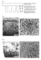
- Fig. 1 is a diagram schematically illustrating a particle size.
- Fig. 1 shows the average diameter D1 at the particle bottom being apart from the bottom of each particle by 10% of the particle length, the average diameter D2 at the particle middle being apart from the bottom of each particle by 50% of the particle length, and the average diameter D3 at the particle end being apart from the bottom of each particle by 90% of the particle length.
- This specification can identify the particle shape.
- the roughened layer of such a copper foil can be formed using a sulfuric acid/copper sulfate electrolytic bath containing at least one material selected from alkyl sulfates, tungsten, and arsenic, and the shape described above can be achieved by appropriately setting electrolytic treatment conditions. Furthermore, a heat-resistant/rustproof layer containing at least one element selected from zinc, nickel, copper, phosphorus, and cobalt can be formed on the roughened layer, a chromate film layer can be formed on the heat-resistant/rustproof layer, and a silane coupling agent layer can be formed on the chromate film layer.
- the unevenness of the roughened surface of the copper foil is transferred to the resin after the removal of the copper layer.
- the unevenness transferred to the resin corresponds to the shapes and number distribution of the roughening particles on the copper foil surface and is important. If the particles of the rough surface of the copper foil have small diameters at the bottom positions, the transferred holes have small diameters, and the sum of areas of the holes is small.
- the roughened layer composed of acicular or rod-like fine roughening particles of copper can be produced using a sulfuric acid/copper sulfate electrolytic bath containing at least one material selected from alkyl sulfates, tungsten, and arsenic.
- the roughened layer composed of acicular fine roughening particles of copper is preferably subjected to overlay plating in a sulfuric acid/copper sulfate electrolytic bath for preventing powder fall and improving the peel strength.
- the copper foil for printed wiring boards of the present invention includes acicular fine roughening particles on at least one surface of the copper foil instead of the roundish or spherical projections or dendrite-like crystal grains that have been conventionally believed to be good for roughening treatment.
- the adhesion strength between the copper foil itself and a resin is increased, and it is thereby possible to provide high peel strength to a substrate for package in chemical treatment during fine-pattern formation.
- the present invention has a notable effect of providing a copper foil that allows fine etching and a method of producing the copper foil.
- the copper foil was laminated to the resin (MBT-830) as described above, and peel strengths of the laminate in a normal state and after heating were measured. The results are shown in Table 2.
- a copper layer was formed under the same conditions as those in Example 3 except that a Cr/CuP intermediate layer was formed between the carrier and the copper foil.
- the Cr/CuP intermediate layer was produced by plating in a plating solution having the following liquid composition.
- a copper layer was formed under the same conditions as those in Example 4 except that a Co/chromate treated intermediate layer was formed between the carrier and the copper foil.
- the circuit width for the peel strength was 10 mm.
- the peel strength in a normal state was 0.91 kg/cm, and the peel strength after heating was 0.84 kg/cm. Both peel strengths were higher than those in Comparative Examples as described.
- the copper foil with a carrier for a printed circuit board of the present invention is significantly effective as a copper foil for printed circuits (copper foil for a semiconductor package substrate) or a substrate for semiconductor package composed of a copper foil for a semiconductor package substrate and a resin for semiconductor package bonded to each other.
Landscapes
- Engineering & Computer Science (AREA)
- Microelectronics & Electronic Packaging (AREA)
- Chemical & Material Sciences (AREA)
- Manufacturing & Machinery (AREA)
- Organic Chemistry (AREA)
- Materials Engineering (AREA)
- Metallurgy (AREA)
- Chemical Kinetics & Catalysis (AREA)
- Electrochemistry (AREA)
- Inorganic Chemistry (AREA)
- Mechanical Engineering (AREA)
- Ceramic Engineering (AREA)
- Laminated Bodies (AREA)
- Parts Printed On Printed Circuit Boards (AREA)
- Electroplating Methods And Accessories (AREA)
- Manufacturing Of Printed Wiring (AREA)
- Manufacturing Of Printed Circuit Boards (AREA)
Applications Claiming Priority (2)
| Application Number | Priority Date | Filing Date | Title |
|---|---|---|---|
| JP2012069660A JP5204908B1 (ja) | 2012-03-26 | 2012-03-26 | キャリア付銅箔、キャリア付銅箔の製造方法、プリント配線板用キャリア付銅箔及びプリント配線板 |
| EP13767488.3A EP2826623B1 (fr) | 2012-03-26 | 2013-03-26 | Feuille de cuivre dotée d'un support, procédé permettant de fabriquer une feuille de cuivre dotée d'un support, procédé de fabrication d'une carte de circuit imprimé |
Related Parent Applications (2)
| Application Number | Title | Priority Date | Filing Date |
|---|---|---|---|
| EP13767488.3A Division-Into EP2826623B1 (fr) | 2012-03-26 | 2013-03-26 | Feuille de cuivre dotée d'un support, procédé permettant de fabriquer une feuille de cuivre dotée d'un support, procédé de fabrication d'une carte de circuit imprimé |
| EP13767488.3A Division EP2826623B1 (fr) | 2012-03-26 | 2013-03-26 | Feuille de cuivre dotée d'un support, procédé permettant de fabriquer une feuille de cuivre dotée d'un support, procédé de fabrication d'une carte de circuit imprimé |
Publications (2)
| Publication Number | Publication Date |
|---|---|
| EP3000904A2 true EP3000904A2 (fr) | 2016-03-30 |
| EP3000904A3 EP3000904A3 (fr) | 2016-04-20 |
Family
ID=48713052
Family Applications (4)
| Application Number | Title | Priority Date | Filing Date |
|---|---|---|---|
| EP15170556.3A Ceased EP3000904A3 (fr) | 2012-03-26 | 2013-03-26 | Feuille de cuivre avec support, procédé de production associé, feuille de cuivre avec support pour carte de circuit imprimé et une telle carte |
| EP16166102.0A Ceased EP3072682A1 (fr) | 2012-03-26 | 2013-03-26 | Carte de circuit imprimé et son procédé de fabrication |
| EP19151697.0A Withdrawn EP3501817A1 (fr) | 2012-03-26 | 2013-03-26 | Feuille de cuivre avec support, procédé de production associé, feuille de cuivre avec support pour carte de circuit imprimé et une telle carte |
| EP13767488.3A Active EP2826623B1 (fr) | 2012-03-26 | 2013-03-26 | Feuille de cuivre dotée d'un support, procédé permettant de fabriquer une feuille de cuivre dotée d'un support, procédé de fabrication d'une carte de circuit imprimé |
Family Applications After (3)
| Application Number | Title | Priority Date | Filing Date |
|---|---|---|---|
| EP16166102.0A Ceased EP3072682A1 (fr) | 2012-03-26 | 2013-03-26 | Carte de circuit imprimé et son procédé de fabrication |
| EP19151697.0A Withdrawn EP3501817A1 (fr) | 2012-03-26 | 2013-03-26 | Feuille de cuivre avec support, procédé de production associé, feuille de cuivre avec support pour carte de circuit imprimé et une telle carte |
| EP13767488.3A Active EP2826623B1 (fr) | 2012-03-26 | 2013-03-26 | Feuille de cuivre dotée d'un support, procédé permettant de fabriquer une feuille de cuivre dotée d'un support, procédé de fabrication d'une carte de circuit imprimé |
Country Status (9)
| Country | Link |
|---|---|
| US (2) | US9578741B2 (fr) |
| EP (4) | EP3000904A3 (fr) |
| JP (1) | JP5204908B1 (fr) |
| KR (4) | KR101672173B1 (fr) |
| CN (4) | CN105555059B (fr) |
| MY (2) | MY165925A (fr) |
| PH (3) | PH12020500253A1 (fr) |
| TW (1) | TWI508850B (fr) |
| WO (1) | WO2013146717A1 (fr) |
Families Citing this family (58)
| Publication number | Priority date | Publication date | Assignee | Title |
|---|---|---|---|---|
| KR20150020621A (ko) * | 2012-06-04 | 2015-02-26 | 제이엑스 닛코 닛세키 킨조쿠 가부시키가이샤 | 다층 프린트 배선판의 제조 방법 |
| JP6013475B2 (ja) * | 2012-06-04 | 2016-10-25 | Jx金属株式会社 | キャリア付金属箔 |
| CN104619486B (zh) * | 2012-06-04 | 2018-01-26 | Jx日矿日石金属株式会社 | 附载体金属箔 |
| KR20150024353A (ko) * | 2012-06-04 | 2015-03-06 | 제이엑스 닛코 닛세키 킨조쿠 가부시키가이샤 | 캐리어 부착 금속박 |
| CN109951964A (zh) | 2013-07-23 | 2019-06-28 | Jx日矿日石金属株式会社 | 表面处理铜箔、附载体铜箔、基材、及树脂基材 |
| JP6166614B2 (ja) * | 2013-07-23 | 2017-07-19 | Jx金属株式会社 | 表面処理銅箔、キャリア付銅箔、基材、プリント配線板、プリント回路板、銅張積層板及びプリント配線板の製造方法 |
| EP3026144A4 (fr) * | 2013-07-24 | 2017-04-12 | JX Nippon Mining & Metals Corp. | Feuille de cuivre traitée en surface, feuille de cuivre comprenant un transporteur, substrat, substrat de résine, carte de circuit imprimé, stratifié plaqué cuivre, et procédé de production de carte de circuit imprimé |
| JP2015043419A (ja) * | 2013-07-24 | 2015-03-05 | Jx日鉱日石金属株式会社 | 樹脂基材、銅張積層板、プリント配線板、電子機器及びプリント配線板の製造方法 |
| JP6593979B2 (ja) * | 2013-07-24 | 2019-10-23 | Jx金属株式会社 | 表面処理銅箔、キャリア付銅箔、基材、銅張積層板の製造方法、電子機器の製造方法及びプリント配線板の製造方法 |
| JP5885791B2 (ja) * | 2013-08-20 | 2016-03-15 | Jx金属株式会社 | 表面処理銅箔及びそれを用いた積層板、キャリア付銅箔、銅箔、プリント配線板、電子機器、電子機器の製造方法、並びに、プリント配線板の製造方法 |
| WO2015040998A1 (fr) * | 2013-09-20 | 2015-03-26 | 三井金属鉱業株式会社 | Feuille de cuivre, feuille de cuivre ayant une feuille de support, et stratifié plaqué de cuivre |
| JP6591766B2 (ja) * | 2014-04-24 | 2019-10-16 | Jx金属株式会社 | キャリア付銅箔、プリント配線板、積層体、電子機器及びプリント配線板の製造方法 |
| JP5823005B1 (ja) * | 2014-08-29 | 2015-11-25 | Jx日鉱日石金属株式会社 | キャリア付銅箔の製造方法、銅張積層板の製造方法、プリント配線板の製造方法、及び、電子機器及びキャリア付銅箔 |
| JP5972486B1 (ja) * | 2014-09-05 | 2016-08-17 | 古河電気工業株式会社 | 銅箔、銅張積層板、および基板 |
| JP6367687B2 (ja) * | 2014-10-30 | 2018-08-01 | Jx金属株式会社 | 表面処理銅箔及び積層板 |
| JP6373166B2 (ja) * | 2014-10-30 | 2018-08-15 | Jx金属株式会社 | 表面処理銅箔及び積層板 |
| JP6640567B2 (ja) | 2015-01-16 | 2020-02-05 | Jx金属株式会社 | キャリア付銅箔、積層体、プリント配線板、電子機器の製造方法及びプリント配線板の製造方法 |
| JP6392674B2 (ja) * | 2015-01-23 | 2018-09-19 | Jx金属株式会社 | 表面処理銅箔及び積層板 |
| JP6379055B2 (ja) * | 2015-01-30 | 2018-08-22 | Jx金属株式会社 | 表面処理銅箔及び積層板 |
| MY186266A (en) * | 2015-03-31 | 2021-07-01 | Mitsui Mining & Smelting Co Ltd | Roughened copper foil, copper foil provided with carrier, copper-clad laminated sheet, and printed wiring board |
| US10264720B1 (en) | 2015-06-23 | 2019-04-16 | Flextronics Ap, Llc | Lead trimming module |
| JP6432684B2 (ja) * | 2015-07-31 | 2018-12-05 | 住友金属鉱山株式会社 | 導電性基板、導電性基板の製造方法 |
| CN107709629B (zh) * | 2015-08-12 | 2019-12-10 | 古河电气工业株式会社 | 表面处理铜箔以及使用该表面处理铜箔制造的覆铜层压板或印刷布线板 |
| WO2017026490A1 (fr) * | 2015-08-12 | 2017-02-16 | 古河電気工業株式会社 | Feuille de cuivre pour circuit à haute fréquence, feuille stratifiée recouverte de cuivre, et carte de circuit imprimé |
| CN106550542B (zh) * | 2015-09-17 | 2021-10-26 | 奥特斯(中国)有限公司 | 插入保护结构并且靠近保护结构具有纯介质层的部件载体 |
| JPWO2017051897A1 (ja) * | 2015-09-24 | 2018-08-30 | Jx金属株式会社 | 金属箔、離型層付き金属箔、積層体、プリント配線板、半導体パッケージ、電子機器及びプリント配線板の製造方法 |
| US10321560B2 (en) * | 2015-11-12 | 2019-06-11 | Multek Technologies Limited | Dummy core plus plating resist restrict resin process and structure |
| US10064292B2 (en) | 2016-03-21 | 2018-08-28 | Multek Technologies Limited | Recessed cavity in printed circuit board protected by LPI |
| WO2017179416A1 (fr) * | 2016-04-14 | 2017-10-19 | 三井金属鉱業株式会社 | Feuille de cuivre traitée en surface, feuille de cuivre avec support et procédés de fabrication de stratifié revêtu de cuivre et carte de circuit imprimé l'utilisant |
| US10712398B1 (en) | 2016-06-21 | 2020-07-14 | Multek Technologies Limited | Measuring complex PCB-based interconnects in a production environment |
| CN106350862B (zh) * | 2016-08-30 | 2018-08-24 | 灵宝金源朝辉铜业有限公司 | 一种压延铜箔粗化处理方法 |
| JP7409760B2 (ja) * | 2016-12-05 | 2024-01-09 | Jx金属株式会社 | 表面処理銅箔、キャリア付銅箔、積層体、プリント配線板の製造方法及び電子機器の製造方法 |
| US10820414B2 (en) * | 2016-12-05 | 2020-10-27 | Jx Nippon Mining & Metals Corporation | Surface treated copper foil, copper foil with carrier, laminate, method for manufacturing printed wiring board, and method for manufacturing electronic device |
| JP7492807B2 (ja) * | 2016-12-06 | 2024-05-30 | Jx金属株式会社 | 表面処理銅箔、キャリア付銅箔、積層体、プリント配線板の製造方法及び電子機器の製造方法 |
| CN109937479B (zh) * | 2016-12-27 | 2023-01-13 | 古河电气工业株式会社 | 引线框材料及其制造方法以及半导体封装件 |
| JP6890301B2 (ja) * | 2017-02-23 | 2021-06-18 | パナソニックIpマネジメント株式会社 | プリント配線板及びプリント配線板の製造方法 |
| JP7356209B2 (ja) * | 2017-03-31 | 2023-10-04 | Jx金属株式会社 | 表面処理銅箔、樹脂層付き表面処理銅箔、キャリア付銅箔、積層体、プリント配線板の製造方法及び電子機器の製造方法 |
| CN108696987B (zh) * | 2017-03-31 | 2021-11-30 | Jx金属株式会社 | 表面处理铜箔、附有载体的铜箔、积层体、印刷布线板的制造方法及电子机器的制造方法 |
| JP7492808B2 (ja) * | 2017-03-31 | 2024-05-30 | Jx金属株式会社 | 表面処理銅箔、樹脂層付き表面処理銅箔、キャリア付銅箔、積層体、プリント配線板の製造方法及び電子機器の製造方法 |
| JP6550196B2 (ja) * | 2017-07-24 | 2019-07-24 | 古河電気工業株式会社 | 表面処理銅箔、並びにこれを用いた銅張積層板およびプリント配線板 |
| US10182494B1 (en) | 2017-09-07 | 2019-01-15 | Flex Ltd. | Landless via concept |
| JP6806951B2 (ja) * | 2018-02-20 | 2021-01-06 | 三井金属鉱業株式会社 | ガラスキャリア付銅箔及びその製造方法 |
| JP6606317B1 (ja) * | 2018-04-25 | 2019-11-13 | 古河電気工業株式会社 | 表面処理銅箔、銅張積層板、及びプリント配線板 |
| EP3786315A4 (fr) | 2018-04-27 | 2022-04-20 | JX Nippon Mining & Metals Corporation | Feuille de cuivre traitée en surface, stratifié recouvert de cuivre et carte de circuits imprimés |
| US10697082B1 (en) * | 2019-08-12 | 2020-06-30 | Chang Chun Petrochemical Co., Ltd. | Surface-treated copper foil |
| JP7554057B2 (ja) * | 2020-04-02 | 2024-09-19 | マクセル株式会社 | 回路部品及び回路部品の製造方法 |
| KR102454686B1 (ko) * | 2020-12-30 | 2022-10-13 | 에스케이씨 주식회사 | 표면 처리 동박 및 이를 포함하는 회로 기판 |
| JP7632594B2 (ja) * | 2021-03-26 | 2025-02-19 | 三菱マテリアル株式会社 | 金属板材、積層体、絶縁回路基板、および、金属板材の製造方法 |
| JPWO2022244826A1 (fr) * | 2021-05-20 | 2022-11-24 | ||
| CN113099605B (zh) * | 2021-06-08 | 2022-07-12 | 广州方邦电子股份有限公司 | 金属箔、带载体金属箔、覆铜层叠板及印刷线路板 |
| KR102517417B1 (ko) * | 2021-07-09 | 2023-04-03 | 주식회사 다이브 | 반도체용 동박의 제조방법 및 이를 이용한 반도체용 동박 |
| KR102950133B1 (ko) * | 2021-09-30 | 2026-04-09 | 롯데에너지머티리얼즈 주식회사 | 미세 홀 가공이 용이한 캐리어박 부착 극박동박, 및 이를 포함하는 동박 적층판, 그의 제조방법 |
| CN118843718A (zh) * | 2022-03-24 | 2024-10-25 | 三井金属矿业株式会社 | 粗糙化处理铜箔、带载体的铜箔、覆铜层叠板及印刷电路板 |
| WO2023182175A1 (fr) * | 2022-03-24 | 2023-09-28 | 三井金属鉱業株式会社 | Feuille de cuivre rugosifiée, feuille de cuivre fixée à un support, stratifié plaqué de cuivre et carte de circuits imprimés |
| KR20240166997A (ko) * | 2022-03-24 | 2024-11-26 | 미쓰이금속광업주식회사 | 조화 처리 동박, 캐리어 구비 동박, 동장 적층판 및 프린트 배선판 |
| WO2023182174A1 (fr) * | 2022-03-24 | 2023-09-28 | 三井金属鉱業株式会社 | Feuille de cuivre rendue rugueuse, feuille de cuivre pourvue d'un support, stratifié plaqué de cuivre et carte de circuit imprimé |
| CN117926350A (zh) * | 2024-01-11 | 2024-04-26 | 九江德福科技股份有限公司 | 一种可剥离负载体铜箔的生产方法 |
| CN120888920B (zh) * | 2025-07-31 | 2026-03-10 | 广东嘉元科技股份有限公司 | 一种ic封装用铜箔的生产方法 |
Citations (8)
| Publication number | Priority date | Publication date | Assignee | Title |
|---|---|---|---|---|
| JPS5135711A (en) | 1974-09-24 | 1976-03-26 | Komatsu Shoichi | Taisui hatsuyuseiojusurukami narabini sonoseizoho |
| JPS546701A (en) | 1977-06-17 | 1979-01-19 | Matsushita Electric Ind Co Ltd | Channel selector |
| JPH03122298A (ja) | 1989-10-06 | 1991-05-24 | Nikko Guurudo Fuoiru Kk | 銅箔の電解処理方法 |
| JPH08236930A (ja) | 1995-02-23 | 1996-09-13 | Nikko Gould Foil Kk | 印刷回路用銅箔及びその製造方法 |
| JP2002170827A (ja) | 2000-09-25 | 2002-06-14 | Ibiden Co Ltd | 半導体素子の製造方法 |
| JP3306404B2 (ja) | 2000-01-28 | 2002-07-24 | 三井金属鉱業株式会社 | 表面処理銅箔の製造方法及びその製造方法で得られた表面処理銅箔を用いた銅張積層板 |
| JP3459964B2 (ja) | 1994-01-21 | 2003-10-27 | オリン コーポレーション | 銅ホイルのためのノジュラー銅・ニッケル合金処理方法 |
| WO2004005588A1 (fr) | 2002-07-04 | 2004-01-15 | Mitsui Mining & Smelting Co.,Ltd. | Feuille de cuivre electrolytique avec feuille de support |
Family Cites Families (37)
| Publication number | Priority date | Publication date | Assignee | Title |
|---|---|---|---|---|
| US3585010A (en) | 1968-10-03 | 1971-06-15 | Clevite Corp | Printed circuit board and method of making same |
| JPS546701B1 (fr) | 1972-03-21 | 1979-03-30 | ||
| JP3471046B2 (ja) * | 1993-08-12 | 2003-11-25 | 富士通株式会社 | プリント基板の製造方法 |
| TW462922B (en) * | 1996-03-21 | 2001-11-11 | Hitachi Chemical Co Ltd | Copper-clad laminate, multilayer copper-clad laminate and process for producing the same |
| JP2000244085A (ja) * | 1999-02-19 | 2000-09-08 | Hitachi Aic Inc | プリント配線板およびその製造方法 |
| JP2000269637A (ja) | 1999-03-18 | 2000-09-29 | Furukawa Circuit Foil Kk | 高密度超微細配線板用銅箔 |
| JP2000294922A (ja) * | 1999-04-01 | 2000-10-20 | Victor Co Of Japan Ltd | 多層プリント配線板用の絶縁樹脂組成物 |
| JP3466506B2 (ja) * | 1999-04-23 | 2003-11-10 | 三井金属鉱業株式会社 | キャリア箔付電解銅箔及びその電解銅箔の製造方法並びにその電解銅箔を使用した銅張積層板 |
| JP3370624B2 (ja) | 1999-08-24 | 2003-01-27 | 三井金属鉱業株式会社 | キャリア箔付電解銅箔及びその電解銅箔を使用した銅張積層板 |
| JP2001068804A (ja) * | 1999-08-31 | 2001-03-16 | Mitsui Mining & Smelting Co Ltd | キャリア箔付電解銅箔及びその電解銅箔の製造方法並びにその電解銅箔を使用した銅張積層板 |
| JP2002069691A (ja) * | 2000-08-31 | 2002-03-08 | Nippon Denkai Kk | 印刷回路基板用銅箔の製造方法 |
| US7026059B2 (en) * | 2000-09-22 | 2006-04-11 | Circuit Foil Japan Co., Ltd. | Copper foil for high-density ultrafine printed wiring boad |
| JP2003051673A (ja) * | 2001-08-06 | 2003-02-21 | Mitsui Mining & Smelting Co Ltd | プリント配線板用銅箔及びそのプリント配線板用銅箔を用いた銅張積層板 |
| JP4379854B2 (ja) | 2001-10-30 | 2009-12-09 | 日鉱金属株式会社 | 表面処理銅箔 |
| JP3812834B2 (ja) * | 2002-08-12 | 2006-08-23 | 三井金属鉱業株式会社 | キャリア箔付電解銅箔並びにその製造方法及びそのキャリア箔付電解銅箔を用いた銅張積層板 |
| TW200420208A (en) * | 2002-10-31 | 2004-10-01 | Furukawa Circuit Foil | Ultra-thin copper foil with carrier, method of production of the same, and printed circuit board using ultra-thin copper foil with carrier |
| JP2005008955A (ja) * | 2003-06-19 | 2005-01-13 | Hitachi Cable Ltd | 銅箔の表面処理方法 |
| JP2005048277A (ja) * | 2003-07-15 | 2005-02-24 | Mitsui Mining & Smelting Co Ltd | キャリア箔付電解銅箔及びそのキャリア箔付電解銅箔の製造方法 |
| EP1531656A3 (fr) * | 2003-11-11 | 2007-10-03 | Furukawa Circuit Foil Co., Ltd. | Feuille de cuivre ultra-mince avec support et panneau à circuit imprimé utilisant une feuille de cuivre ultra-mince avec support |
| JP3933128B2 (ja) * | 2003-12-26 | 2007-06-20 | 松下電工株式会社 | 金属箔付き樹脂フィルム、金属箔付き樹脂シート、金属張り積層板 |
| TW200535259A (en) * | 2004-02-06 | 2005-11-01 | Furukawa Circuit Foil | Treated copper foil and circuit board |
| JP2006103189A (ja) | 2004-10-06 | 2006-04-20 | Furukawa Circuit Foil Kk | 表面処理銅箔並びに回路基板 |
| JP4904933B2 (ja) * | 2005-09-27 | 2012-03-28 | 日立電線株式会社 | ニッケルめっき液とその製造方法、ニッケルめっき方法およびプリント配線板用銅箔 |
| CN1984527B (zh) * | 2005-12-15 | 2010-12-01 | 古河电气工业株式会社 | 带载体的极薄铜箔及印刷电路基板 |
| JP4934409B2 (ja) * | 2005-12-15 | 2012-05-16 | 古河電気工業株式会社 | キャリア付き極薄銅箔及びプリント配線基板 |
| TW200804626A (en) * | 2006-05-19 | 2008-01-16 | Mitsui Mining & Smelting Co | Copper foil provided with carrier sheet, method for fabricating copper foil provided with carrier sheet, surface-treated copper foil provided with carrier sheet, and copper-clad laminate using the surface-treated copper foil provided with carrier she |
| CN101466875B (zh) * | 2006-06-12 | 2011-01-05 | 日矿金属株式会社 | 具有粗化处理面的轧制铜或铜合金箔以及该轧制铜或铜合金箔的粗化方法 |
| TWI434965B (zh) | 2008-05-28 | 2014-04-21 | Mitsui Mining & Smelting Co | A roughening method for copper foil, and a copper foil for a printed wiring board which is obtained by the roughening method |
| EP2336395A1 (fr) * | 2008-09-05 | 2011-06-22 | Furukawa Electric Co., Ltd. | Feuille ultramince de cuivre sur support, et carte ou circuit imprimé de connexion |
| US20110281126A1 (en) * | 2008-12-26 | 2011-11-17 | Mitsuru Nozaki | Resin composite copper foil |
| KR20130054447A (ko) * | 2009-03-27 | 2013-05-24 | 제이엑스 닛코 닛세키 킨조쿠 가부시키가이샤 | 프린트 배선판용 동박 및 그 제조 방법 |
| KR101682886B1 (ko) * | 2009-07-14 | 2016-12-06 | 아지노모토 가부시키가이샤 | 동박이 부착된 접착 필름 |
| CN102574365B (zh) * | 2009-07-24 | 2015-11-25 | 三菱瓦斯化学株式会社 | 树脂复合电解铜箔、覆铜层压板和印刷线路板 |
| CN101892499B (zh) * | 2010-07-24 | 2011-11-09 | 江西理工大学 | 以铜箔作载体的可剥离超薄铜箔及其制备方法 |
| US20130189538A1 (en) * | 2010-09-24 | 2013-07-25 | Jx Nippon Mining & Metals Corporation | Method of manufacturing copper foil for printed wiring board, and copper foil printed wiring board |
| PH12013500540B1 (en) * | 2010-09-27 | 2020-02-14 | Jx Nippon Mining & Metals Corp | Copper foil for printed wiring board, method for producing said copper foil, resin substrate for printed wiring board, and printed wiring board |
| JP5417538B1 (ja) * | 2012-06-11 | 2014-02-19 | Jx日鉱日石金属株式会社 | 表面処理銅箔及びそれを用いた積層板、プリント配線板、電子機器、並びに、プリント配線板の製造方法 |
-
2012
- 2012-03-26 JP JP2012069660A patent/JP5204908B1/ja not_active Expired - Fee Related
-
2013
- 2013-03-26 WO PCT/JP2013/058653 patent/WO2013146717A1/fr not_active Ceased
- 2013-03-26 CN CN201610069512.2A patent/CN105555059B/zh not_active Expired - Fee Related
- 2013-03-26 US US14/388,381 patent/US9578741B2/en not_active Expired - Fee Related
- 2013-03-26 MY MYPI2014702830A patent/MY165925A/en unknown
- 2013-03-26 KR KR1020157013888A patent/KR101672173B1/ko not_active Expired - Fee Related
- 2013-03-26 KR KR1020147029562A patent/KR101632822B1/ko not_active Expired - Fee Related
- 2013-03-26 EP EP15170556.3A patent/EP3000904A3/fr not_active Ceased
- 2013-03-26 CN CN201380017079.2A patent/CN104220250B/zh not_active Expired - Fee Related
- 2013-03-26 KR KR1020157013889A patent/KR101672176B1/ko not_active Expired - Fee Related
- 2013-03-26 CN CN201610090046.6A patent/CN105682347A/zh active Pending
- 2013-03-26 TW TW102110640A patent/TWI508850B/zh not_active IP Right Cessation
- 2013-03-26 EP EP16166102.0A patent/EP3072682A1/fr not_active Ceased
- 2013-03-26 EP EP19151697.0A patent/EP3501817A1/fr not_active Withdrawn
- 2013-03-26 EP EP13767488.3A patent/EP2826623B1/fr active Active
- 2013-03-26 CN CN201610069442.0A patent/CN105682375B/zh not_active Expired - Fee Related
- 2013-03-26 PH PH1/2020/500253A patent/PH12020500253A1/en unknown
- 2013-03-26 KR KR1020167017049A patent/KR101822314B1/ko not_active Expired - Fee Related
- 2013-03-26 PH PH1/2020/500254A patent/PH12020500254A1/en unknown
- 2013-03-26 MY MYPI2018700795A patent/MY170684A/en unknown
-
2014
- 2014-09-26 PH PH12014502150A patent/PH12014502150A1/en unknown
-
2016
- 2016-04-27 US US15/139,482 patent/US9788423B2/en not_active Expired - Fee Related
Patent Citations (8)
| Publication number | Priority date | Publication date | Assignee | Title |
|---|---|---|---|---|
| JPS5135711A (en) | 1974-09-24 | 1976-03-26 | Komatsu Shoichi | Taisui hatsuyuseiojusurukami narabini sonoseizoho |
| JPS546701A (en) | 1977-06-17 | 1979-01-19 | Matsushita Electric Ind Co Ltd | Channel selector |
| JPH03122298A (ja) | 1989-10-06 | 1991-05-24 | Nikko Guurudo Fuoiru Kk | 銅箔の電解処理方法 |
| JP3459964B2 (ja) | 1994-01-21 | 2003-10-27 | オリン コーポレーション | 銅ホイルのためのノジュラー銅・ニッケル合金処理方法 |
| JPH08236930A (ja) | 1995-02-23 | 1996-09-13 | Nikko Gould Foil Kk | 印刷回路用銅箔及びその製造方法 |
| JP3306404B2 (ja) | 2000-01-28 | 2002-07-24 | 三井金属鉱業株式会社 | 表面処理銅箔の製造方法及びその製造方法で得られた表面処理銅箔を用いた銅張積層板 |
| JP2002170827A (ja) | 2000-09-25 | 2002-06-14 | Ibiden Co Ltd | 半導体素子の製造方法 |
| WO2004005588A1 (fr) | 2002-07-04 | 2004-01-15 | Mitsui Mining & Smelting Co.,Ltd. | Feuille de cuivre electrolytique avec feuille de support |
Also Published As
Similar Documents
| Publication | Publication Date | Title |
|---|---|---|
| EP2826623B1 (fr) | Feuille de cuivre dotée d'un support, procédé permettant de fabriquer une feuille de cuivre dotée d'un support, procédé de fabrication d'une carte de circuit imprimé | |
| KR101822251B1 (ko) | 구리박, 캐리어 부착 구리박, 구리 피복 적층체, 프린트 배선판, 반도체 패키지용 회로 형성 기판, 반도체 패키지, 전자 기기, 수지 기재, 회로의 형성 방법, 세미 애디티브 공법, 프린트 배선판의 제조 방법 | |
| KR101607381B1 (ko) | 고주파 회로용 동박, 고주파 회로용 구리 피복 적층판, 고주파 회로용 프린트 배선판, 고주파 회로용 캐리어가 부착된 동박, 전자 기기, 및 프린트 배선판의 제조 방법 | |
| CN102265710B (zh) | 电子电路用的压延铜箔或电解铜箔及使用它们形成电子电路的方法 | |
| JP5457594B2 (ja) | プリント配線板用樹脂、プリント配線板、半導体パッケージ基板及びプリント配線板の製造方法 | |
| JP2014195871A (ja) | キャリア付銅箔、キャリア付銅箔の製造方法、プリント配線板、プリント回路板、銅張積層板、及び、プリント配線板の製造方法 | |
| JP5298252B1 (ja) | キャリア付銅箔、キャリア付銅箔の製造方法、プリント配線板、プリント回路板、銅張積層板、及び、プリント配線板の製造方法 | |
| JP5449596B1 (ja) | キャリア付銅箔、キャリア付銅箔の製造方法、プリント配線板、プリント回路板、銅張積層板、及び、プリント配線板の製造方法 | |
| JP5399582B2 (ja) | キャリア付銅箔、キャリア付銅箔の製造方法、プリント配線板用キャリア付銅箔及びプリント配線板 | |
| JP6329727B2 (ja) | キャリア付銅箔、キャリア付銅箔の製造方法、プリント配線板、プリント回路板、銅張積層板、及び、プリント配線板の製造方法 | |
| JP6329731B2 (ja) | キャリア付銅箔、銅張積層板の製造方法、及びプリント配線板の製造方法 | |
| JP5285180B1 (ja) | キャリア付銅箔、キャリア付銅箔の製造方法、プリント配線板用キャリア付銅箔及びプリント配線板 | |
| JP2014195036A (ja) | キャリア付銅箔、キャリア付銅箔の製造方法、プリント配線板、プリント回路板、銅張積層板、及びプリント配線板の製造方法 |
Legal Events
| Date | Code | Title | Description |
|---|---|---|---|
| PUAL | Search report despatched |
Free format text: ORIGINAL CODE: 0009013 |
|
| PUAI | Public reference made under article 153(3) epc to a published international application that has entered the european phase |
Free format text: ORIGINAL CODE: 0009012 |
|
| AC | Divisional application: reference to earlier application |
Ref document number: 2826623 Country of ref document: EP Kind code of ref document: P |
|
| AK | Designated contracting states |
Kind code of ref document: A2 Designated state(s): AL AT BE BG CH CY CZ DE DK EE ES FI FR GB GR HR HU IE IS IT LI LT LU LV MC MK MT NL NO PL PT RO RS SE SI SK SM TR |
|
| AK | Designated contracting states |
Kind code of ref document: A3 Designated state(s): AL AT BE BG CH CY CZ DE DK EE ES FI FR GB GR HR HU IE IS IT LI LT LU LV MC MK MT NL NO PL PT RO RS SE SI SK SM TR |
|
| 17P | Request for examination filed |
Effective date: 20161019 |
|
| RBV | Designated contracting states (corrected) |
Designated state(s): AL AT BE BG CH CY CZ DE DK EE ES FI FR GB GR HR HU IE IS IT LI LT LU LV MC MK MT NL NO PL PT RO RS SE SI SK SM TR |
|
| STAA | Information on the status of an ep patent application or granted ep patent |
Free format text: STATUS: EXAMINATION IS IN PROGRESS |
|
| 17Q | First examination report despatched |
Effective date: 20170612 |
|
| STAA | Information on the status of an ep patent application or granted ep patent |
Free format text: STATUS: THE APPLICATION HAS BEEN REFUSED |
|
| 18R | Application refused |
Effective date: 20190207 |