EP3073280B1 - Tester für integrierte schaltkreise auf einem silizium-wafer, und integrierter schaltkreis - Google Patents
Tester für integrierte schaltkreise auf einem silizium-wafer, und integrierter schaltkreis Download PDFInfo
- Publication number
- EP3073280B1 EP3073280B1 EP16158167.3A EP16158167A EP3073280B1 EP 3073280 B1 EP3073280 B1 EP 3073280B1 EP 16158167 A EP16158167 A EP 16158167A EP 3073280 B1 EP3073280 B1 EP 3073280B1
- Authority
- EP
- European Patent Office
- Prior art keywords
- integrated circuit
- data
- data frame
- time reference
- command
- Prior art date
- Legal status (The legal status is an assumption and is not a legal conclusion. Google has not performed a legal analysis and makes no representation as to the accuracy of the status listed.)
- Active
Links
Images



Classifications
-
- G—PHYSICS
- G01—MEASURING; TESTING
- G01R—MEASURING ELECTRIC VARIABLES; MEASURING MAGNETIC VARIABLES
- G01R31/00—Arrangements for testing electric properties; Arrangements for locating electric faults; Arrangements for electrical testing characterised by what is being tested not provided for elsewhere
- G01R31/28—Testing of electronic circuits, e.g. by signal tracer
- G01R31/2851—Testing of integrated circuits [IC]
- G01R31/2884—Testing of integrated circuits [IC] using dedicated test connectors, test elements or test circuits on the IC under test
-
- G—PHYSICS
- G01—MEASURING; TESTING
- G01R—MEASURING ELECTRIC VARIABLES; MEASURING MAGNETIC VARIABLES
- G01R31/00—Arrangements for testing electric properties; Arrangements for locating electric faults; Arrangements for electrical testing characterised by what is being tested not provided for elsewhere
- G01R31/28—Testing of electronic circuits, e.g. by signal tracer
- G01R31/317—Testing of digital circuits
- G01R31/3177—Testing of logic operation, e.g. by logic analysers
-
- G—PHYSICS
- G01—MEASURING; TESTING
- G01R—MEASURING ELECTRIC VARIABLES; MEASURING MAGNETIC VARIABLES
- G01R31/00—Arrangements for testing electric properties; Arrangements for locating electric faults; Arrangements for electrical testing characterised by what is being tested not provided for elsewhere
- G01R31/28—Testing of electronic circuits, e.g. by signal tracer
- G01R31/2851—Testing of integrated circuits [IC]
-
- G—PHYSICS
- G01—MEASURING; TESTING
- G01R—MEASURING ELECTRIC VARIABLES; MEASURING MAGNETIC VARIABLES
- G01R31/00—Arrangements for testing electric properties; Arrangements for locating electric faults; Arrangements for electrical testing characterised by what is being tested not provided for elsewhere
- G01R31/28—Testing of electronic circuits, e.g. by signal tracer
- G01R31/2851—Testing of integrated circuits [IC]
- G01R31/2882—Testing timing characteristics
-
- G—PHYSICS
- G01—MEASURING; TESTING
- G01R—MEASURING ELECTRIC VARIABLES; MEASURING MAGNETIC VARIABLES
- G01R1/00—Details of instruments or arrangements of the types included in groups G01R5/00 - G01R13/00 and G01R31/00
- G01R1/02—General constructional details
- G01R1/04—Housings; Supporting members; Arrangements of terminals
- G01R1/0408—Test fixtures or contact fields; Connectors or connecting adaptors; Test clips; Test sockets
- G01R1/0491—Test fixtures or contact fields; Connectors or connecting adaptors; Test clips; Test sockets for testing integrated circuits on wafers, e.g. wafer-level test cartridge
-
- G—PHYSICS
- G01—MEASURING; TESTING
- G01R—MEASURING ELECTRIC VARIABLES; MEASURING MAGNETIC VARIABLES
- G01R31/00—Arrangements for testing electric properties; Arrangements for locating electric faults; Arrangements for electrical testing characterised by what is being tested not provided for elsewhere
- G01R31/28—Testing of electronic circuits, e.g. by signal tracer
- G01R31/2851—Testing of integrated circuits [IC]
- G01R31/2855—Environmental, reliability or burn-in testing
- G01R31/2856—Internal circuit aspects, e.g. built-in test features; Test chips; Measuring material aspects, e.g. electro migration [EM]
-
- G—PHYSICS
- G01—MEASURING; TESTING
- G01R—MEASURING ELECTRIC VARIABLES; MEASURING MAGNETIC VARIABLES
- G01R31/00—Arrangements for testing electric properties; Arrangements for locating electric faults; Arrangements for electrical testing characterised by what is being tested not provided for elsewhere
- G01R31/28—Testing of electronic circuits, e.g. by signal tracer
- G01R31/2851—Testing of integrated circuits [IC]
- G01R31/2855—Environmental, reliability or burn-in testing
- G01R31/286—External aspects, e.g. related to chambers, contacting devices or handlers
- G01R31/2868—Complete testing stations; systems; procedures; software aspects
- G01R31/287—Procedures; Software aspects
-
- G—PHYSICS
- G01—MEASURING; TESTING
- G01R—MEASURING ELECTRIC VARIABLES; MEASURING MAGNETIC VARIABLES
- G01R31/00—Arrangements for testing electric properties; Arrangements for locating electric faults; Arrangements for electrical testing characterised by what is being tested not provided for elsewhere
- G01R31/28—Testing of electronic circuits, e.g. by signal tracer
- G01R31/317—Testing of digital circuits
- G01R31/31712—Input or output aspects
-
- G—PHYSICS
- G01—MEASURING; TESTING
- G01R—MEASURING ELECTRIC VARIABLES; MEASURING MAGNETIC VARIABLES
- G01R31/00—Arrangements for testing electric properties; Arrangements for locating electric faults; Arrangements for electrical testing characterised by what is being tested not provided for elsewhere
- G01R31/28—Testing of electronic circuits, e.g. by signal tracer
- G01R31/317—Testing of digital circuits
- G01R31/31725—Timing aspects, e.g. clock distribution, skew, propagation delay
-
- G—PHYSICS
- G01—MEASURING; TESTING
- G01R—MEASURING ELECTRIC VARIABLES; MEASURING MAGNETIC VARIABLES
- G01R31/00—Arrangements for testing electric properties; Arrangements for locating electric faults; Arrangements for electrical testing characterised by what is being tested not provided for elsewhere
- G01R31/28—Testing of electronic circuits, e.g. by signal tracer
- G01R31/317—Testing of digital circuits
- G01R31/3181—Functional testing
- G01R31/3185—Reconfiguring for testing, e.g. LSSD, partitioning
- G01R31/318505—Test of Modular systems, e.g. Wafers, MCM's
- G01R31/318511—Wafer Test
-
- G—PHYSICS
- G01—MEASURING; TESTING
- G01R—MEASURING ELECTRIC VARIABLES; MEASURING MAGNETIC VARIABLES
- G01R31/00—Arrangements for testing electric properties; Arrangements for locating electric faults; Arrangements for electrical testing characterised by what is being tested not provided for elsewhere
- G01R31/28—Testing of electronic circuits, e.g. by signal tracer
- G01R31/317—Testing of digital circuits
- G01R31/3181—Functional testing
- G01R31/319—Tester hardware, i.e. output processing circuits
- G01R31/31903—Tester hardware, i.e. output processing circuits tester configuration
- G01R31/31908—Tester set-up, e.g. configuring the tester to the device under test [DUT], down loading test patterns
-
- G—PHYSICS
- G01—MEASURING; TESTING
- G01R—MEASURING ELECTRIC VARIABLES; MEASURING MAGNETIC VARIABLES
- G01R31/00—Arrangements for testing electric properties; Arrangements for locating electric faults; Arrangements for electrical testing characterised by what is being tested not provided for elsewhere
- G01R31/28—Testing of electronic circuits, e.g. by signal tracer
- G01R31/317—Testing of digital circuits
- G01R31/3172—Optimisation aspects, e.g. using functional pin as test pin, pin multiplexing
Definitions
- the present invention relates to a method and a device for testing integrated circuits arranged on a silicon wafer.
- the integrated circuits are manufactured on silicon wafers (in English wafer).
- a silicon wafer has a large number of integrated circuits, typically thousands.
- the testers used to test the integrated circuits have a limited quantity of input / output connections with the silicon wafer which cannot be increased.
- the tester comes into contact using a point card (in English probe card) with rectangular areas of the integrated circuit several times to establish an electrical connection with the circuit integrated.
- a point card in English probe card
- Several integrated circuits are tested simultaneously in order to reduce the time for testing the silicon wafer.
- the integrated circuits on the silicon wafers have an internal clock whose frequency varies significantly from one integrated circuit to another. This results in a significant difficulty in the test of integrated circuits.
- the present invention aims to solve the drawbacks of the prior art by proposing a method and a test device in which a single input / output connection is necessary for testing an integrated circuit whose frequency of the internal clock n is not known to the tester.
- the number of integrated circuits tested in parallel is increased.
- the test time of the integrated circuits of a silicon wafer is reduced and the production cost of integrated circuits is reduced even if the frequency of the internal clock of the integrated circuits is not known to the tester.
- the integrated circuits can synchronize with the received data and can process these. It is then no longer necessary to have a dedicated connection for the transmission of a clock common to the integrated circuits and to the tester.
- the constraints such as rising edges, falling edges of the signals transmitted by the integrated circuit are less.
- the characteristics of the electronic elements for example in terms of capacity to supply current can be reduced as the size of these electronic elements. The cost of the integrated circuit is thus also reduced.
- each datum of the data frame transferred to the integrated circuit is represented by a high and low logic level.
- the integrated circuit can continue to synchronize during the reception of the data.
- the data frame transferred to the integrated circuit also includes a value associated with the test command of the integrated circuit.
- the tester can vary certain parameters for testing integrated circuits.
- the test command for the integrated circuit is a command for adjusting an analog or frequency or digital value in the integrated circuit.
- the command is a command for transmitting or receiving an analog signal in a time window according to the data frame and the tester includes means for transmitting or receiving the analog signal in the window temporal following the data frame.
- the command is an adjustment command for the internal clock of the integrated circuit or an adjustment command of a write or erase voltage of a data item in a memory of the integrated circuit.
- the integrated circuit can process the data received.
- the maximum number of tips of a tip card being limited by technological capacities, the increase in the number of chips tested in parallel makes it possible to reduce the cost of the test.
- the present invention makes it possible to optimize the use of the spike card as much as possible.
- the data of the transmitted data frame having a duration multiple of the time reference having a duration multiple of the time reference, the constraints such as rising edges, falling signals transmitted by the integrated circuit are less.
- the characteristics of the electronic elements for example in terms of capacity to supply current can be reduced as the size of these electronic elements. The cost of the integrated circuit is thus also reduced.
- the received data frame further comprises a value associated with the test command of the integrated circuit.
- the test command for the integrated circuit is a command for adjusting an analog or frequency or digital value in the integrated circuit.
- the command is a command for transmitting or receiving an analog signal in a time window according to the data frame and the integrated circuit comprises means for transmitting or receiving the analog signal in the time window following the data frame.
- the command is a command for adjusting the internal clock of the integrated circuit.
- the frequency of the internal clock of the integrated circuit can be adjusted to a value corresponding to a criterion of a specification.
- the command is a command for adjusting a write voltage or for erasing data in a Flash memory of the integrated circuit.
- the integrated circuit on receipt of the command to adjust the write or erase voltage, controls reading means in a memory of the integrated circuit using a state machine to adjust the write or erase voltage.
- the integrated circuit is able to adjust parameters autonomously without exchanging data with the tester.
- the test time is thus reduced.
- the invention also relates to computer programs stored on an information medium, said programs comprising instructions making it possible to implement the methods described above, when they are loaded and executed by a computer system.
- the Fig. 1 represents a system for testing integrated circuits on a silicon wafer.
- a tester Te tests the integrated circuits CI of a silicon wafer DUT using a plurality of point cards coming into contact with the rectangular areas of a group of integrated circuits which are tested in parallel.
- the tester Te is for example a computer which drives one or more tip cards.
- the tester Te tests whether the integrated circuits conform to a specification and allows the adjustment of parameters of the integrated circuits.
- each integrated circuit has a single contact area represented by a black square in the Fig. 1 which is used for testing the integrated circuit.
- a single point is used by the tester Te to test an integrated circuit in addition to the supply points of the integrated circuits.
- an input-output connection is made according to the present invention.
- Fig. 1 three integrated circuits are tested in parallel using a point card comprising the points Cap1 to Cap3.
- a point card comprising the points Cap1 to Cap3.
- a larger number of integrated circuits are tested in parallel, the example of the Fig. 1 being only a simplification of real conditions.
- Each integrated circuit has its own internal clock whose frequency varies from one integrated circuit to another and is different from that of the Te tester.
- both digital and analog signals are exchanged between the integrated circuit CI and the tester Te.
- the adjustment of parameters of the Flash memory of the integrated circuit CI, the selection of certain test modes of the Flash memory make it possible to measure voltages and / or electric currents.
- the use of a single contact area according to the present invention for testing an integrated circuit CI takes this constraint into account.
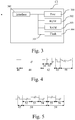
- the Fig. 2 represents an architecture of a test device or tester according to the present invention.
- the processor 200 is capable of executing instructions loaded in the volatile memory 203 from the ROM memory 202, from an external memory (not shown), from a storage medium. When the tester Te is powered up, the processor 200 is capable of reading instructions from the volatile memory 203 and executing them. These instructions form a computer program which causes the implementation, by the processor 200, of all or part of the method described in relation to the Fig. 7 .
- All or part of the process described in relation to the Fig. 7 can be implemented in software form by execution of a set of instructions by a programmable machine, such as a DSP ( Digital Signal Processor in English or Digital Signal Processing Unit in French) or a microcontroller or be implemented in hardware form by a dedicated machine or component, such as an FPGA ( Field-Programmable Gate Array in English or Field Programmable Door Matrix in French) or an ASIC ( Application-Specific Integrated Circuit in English or Integrated Circuit) Specific to an Application in French).
- a programmable machine such as a DSP ( Digital Signal Processor in English or Digital Signal Processing Unit in French) or a microcontroller or be implemented in hardware form by a dedicated machine or component, such as an FPGA ( Field-Programmable Gate Array in English or Field Programmable Door Matrix in French) or an ASIC ( Application-Specific Integrated Circuit in English or Integrated Circuit) Specific to an Application in French).
- a programmable machine such as a DSP ( Digital Signal Processor in English
- the Fig. 3 shows an architecture of an integrated circuit on a silicon wafer according to the present invention.
- Processor 300 is capable of executing instructions loaded into volatile memory 303 from ROM memory 302. When the integrated circuit CI is powered up, processor 300 is capable of reading instructions from volatile memory 303 and execute them. These instructions form a computer program which causes the implementation, by the processor 300, of all or part of the methods described in relation to the Figs. 8 and 9 .
- All or part of the processes described in relation to Figs. 8 and 9 can be implemented in software form by executing a set of instructions by a programmable machine, such as a DSP ( Digital Signal Processor in English or Digital Signal Processing Unit in French) or a microcontroller or be implemented in hardware form by a dedicated machine or component.
- a programmable machine such as a DSP ( Digital Signal Processor in English or Digital Signal Processing Unit in French) or a microcontroller or be implemented in hardware form by a dedicated machine or component.
- the Fig. 4 shows an example of a data frame sent by the tester and intended for integrated circuits.
- the data frame sent by the tester Te and destined for integrated circuits CI is broken down into a time reference 40, a validation field for the time reference 41, data 42 and an end of frame 43.
- the tester Te sends commands to the integrated circuits CI and possibly receives responses to the commands sent.
- the time reference 40 has a duration determined by the frequency of the tester Te.
- the reference 40 corresponds for example to a high logic level whose duration is for example equal to three clock periods of the clock of the tester Te. This duration of three clock periods will be used by the integrated circuit CI to synchronize with the clock of the tester Te.
- the validation field of the time reference 41 corresponds to a low logic level the duration of which is for example equal to a predetermined whole number of times the duration of the time reference 40.
- the validation field has an equal duration at eight times the duration of the time reference 40.
- the time reference validation field 41 allows the integrated circuit CI receiving the data frame to check whether the time reference actually corresponds to the start of a frame or not. If the time reference validation field 41 is not equal to the predetermined number of times the duration of the time reference 40, the time reference 40 is a spurious pulse. If the validation field of the time reference 41 is equal to the predetermined number of times the duration of the time reference 40, a frame is effectively received.
- the data field 42 contains the data necessary for the command sent.
- the data field 42 comprises a succession of binary values "0" or "1".
- the binary value "1" in field 44 corresponds to two clock periods of the clock of the tester Te at the high level followed by a clock period of the clock of the tester Teau low level.
- the binary value "0" in field 45 corresponds to a clock period of the clock of the tester Te at the high level followed by two clock periods of the clock of the tester Te at the low level.
- the integrated circuit CI can, during the reception of the data, continue to synchronize with the clock of the tester Te.
- the binary value "1" corresponds to three clock periods of the clock of the tester Te at the high level and the binary value "0" corresponds to three clock periods of the clock of the tester Te at the low level .
- the end of frame 43 corresponds to two clock periods of the clock of the tester Te at the high level followed by a clock period of the clock of the tester Te at the low level.
- an analog voltage can possibly be transmitted or received.
- This analog voltage is delivered by the integrated circuit CI or by the tester Te.
- This analog voltage is for example a voltage supplied by the tester Te via a command present in the data field or a voltage requested by the tester Te via a command present in the data field.
- the duration 46 can also be a time reference.
- the Fig. 5 shows an example of a data frame sent by an integrated circuit and intended for the tester.
- the integrated circuit CI Upon receipt of an end of frame 43, the integrated circuit CI responds if necessary to the frame as described with reference to Fig. 4 .
- the Fig. 5 represents an end of frame 43 for a digital response of the frame as described with reference to the Fig. 4 , a start of frame 50 and a data field 51.
- the frame includes a start of frame 50.
- the start of frame 50 includes three binary values 52 to 54.
- the clock used by the integrated circuit CI is an integer number of times the duration of the starting field 40 of the frame as described with reference to the Fig. 4 and greater than or equal to twice the duration of the starting field 40.
- the number of times is a multiple of two, preferably equal to eight.
- the integrated circuit CI having to have the smallest possible silicon surface, the output stage delivering the data frames to the tester Te has specifications in terms of current supply much less than the output stage of the tester Te .
- the duration of binary information for the frame transfer of the integrated circuit CI is chosen in such a way that all of the functional integrated circuits can respond at an appropriate rate.
- the binary value 52 is at the low level "0" and has a duration of eight times the duration of the starting field 40.
- the binary value 52 is at the high level "1" and has a duration of eight times the duration of the starting field 40.
- the binary value 53 is at the low level "0" and has a duration of eight times the duration of the starting field 40.
- the data field 51 includes one or more binary values.
- the data field includes two binary values 55 and 56.
- the binary value 55 is at the low level "0" and has a duration of eight times the duration of the starting field 40.
- the binary value 56 is at the high level "1" and has a duration of eight times the duration of the starting field 40.
- the frame sent by the integrated circuit CI does not include an end of frame delimiter. This is not useful because the tester Te knows whether a response is necessary or not and the number of bits if so.
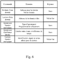
- the Fig. 6 represents examples of commands included in a frame as described with reference to the Fig. 4 .
- the table of the Fig. 6 has three columns, a first column indicates the type of command.
- the type of command in the form of a predetermined binary word, is included in the data field 42 of the frame as described with reference to the Fig. 4 .
- the second column indicates the data that is included in the data field 42.
- the third column indicates whether a response as described with reference to the Fig. 5 or during the period noted 46 in Fig. 6 may or may not be transmitted by the integrated circuit CI. This response is, depending on the type of command, digital, analog or frequency.
- the data field 42 includes the address to which the data must be written as well as the value of the data. No frame should be transmitted in response.
- the data field 42 includes the address at which the data must be read and returned in the data field 51 of the Fig. 5 .
- Field 51 of the frame includes the value of the data read.
- the data field 42 includes the type of adjustment to be made, for example a programming or erasing voltage. No frame should be transmitted in response.
- a parameter table is written in a predetermined area of a memory of the integrated circuit.
- the memory is for example a RAM memory.
- the data field 42 includes the value range in which the frequency of the internal oscillator of the integrated circuit must be adjusted.
- a time reference is inserted in field 46 of the Fig. 4 . No frame should be transmitted in response.
- the integrated circuit CI on receipt of the adjustment command from the internal oscillator, counts the number of pulses produced by the internal oscillator during the time reference indicated by the duration of field 46. If the number of counted pulses is not within the value range, the frequency of the internal oscillator is changed until the number of counted pulses is within the value range.
- the data field 42 includes information indicating which analog signal the tester Te will insert into field 46 of the Fig. 4 as well as the duration of field 46.
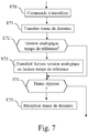
- the Fig. 7 represents a test algorithm executed by the tester according to the present invention.
- the present algorithm is executed by the processor 200 of the tester Te.
- step E70 the processor 200 selects a command to be sent to at least one integrated circuit CI from a list of commands corresponding to tests or adjustments of the parameters of the integrated circuits CI.
- the processor 200 controls the transfer of the data frame as described with reference to the Fig. 4 and which includes the selected command.
- the processor 200 checks whether, for the command, an analog voltage must be transmitted or received or a reference time is included in field 46 of the Fig. 4 .
- step E73 transfers or reads the analog voltage or the reference time for the duration noted 46 in Fig. 4 . If not, the processor 200 goes to step E74.
- step E74 the processor 200 checks whether a frame must be received in response to the frame transmitted in step E71.
- step E71 If a frame is to be received in response to the frame transmitted in step E71, the processor 200 proceeds to step E75. If not, the processor 200 interrupts the present algorithm.
- step E75 the processor 200 receives via the interface 205 the data frame as described with reference to the Fig. 5 .
- the Fig. 8 represents a test algorithm executed by an integrated circuit according to the present invention.
- the present algorithm is executed by the processor 300 of each integrated circuit CI.
- step E80 the processor 300 receives a data frame as described with reference to the Fig. 4 .
- the processor 300 synchronizes with the time reference 40.
- step E81 the processor 300 validates the time reference by checking whether the validation field of the time reference 41 is equal to a predetermined number of times the time reference 40. If not, the processor 300 interrupts the present algorithm waiting for a new time reference 40.
- step E82 the processor 300 processes the data included in the data field 42 and executes the command.
- the processor 300 checks whether, for the command, an analog voltage or a reference time must be transmitted or received or transmitted and received.
- step E84 transfers or reads an analog voltage or measures the reference time for the duration noted 46 in Fig. 4 . If not, the processor 300 goes to step E85.
- step E85 the processor 300 checks whether a data frame must be transmitted in response to the data frame received in step E80.
- step E86 the processor 300 interrupts the present algorithm.
- step E86 the processor 300 transfers via the interface 305 the data frame as described with reference to the Fig. 5 .
- the Fig. 9 represents an algorithm executed by an integrated circuit upon receipt of a command to adjust the programming voltage or erase a Flash memory.
- the present algorithm or state machine is executed by the processor 300 of each integrated circuit CI.
- step E91 the processor 300 controls the transfer of a table comprising different voltage values in the RAM.
- the processor 300 detects the reception of a command to adjust the programming voltage or to erase a memory.
- the memory is for example a Flash memory or E2PROM or MRAM or MLU or CBRAM or FeRAM.
- the processor 300 reads a voltage value from the random access memory and applies the voltage read to the memory.
- the processor 300 checks whether an erasure or a programming has been correctly carried out.
- step E94 the processor 300 goes to step E94 and stores the value read in the RAM.
- step E95 the processor 300 checks whether all the values included in the table have been read.
- step E96 reads another voltage value from the RAM and applies the voltage read to the Flash memory.
Landscapes
- Engineering & Computer Science (AREA)
- Physics & Mathematics (AREA)
- General Physics & Mathematics (AREA)
- General Engineering & Computer Science (AREA)
- Computer Hardware Design (AREA)
- Microelectronics & Electronic Packaging (AREA)
- Environmental & Geological Engineering (AREA)
- Tests Of Electronic Circuits (AREA)
- Semiconductor Integrated Circuits (AREA)
- Testing Or Measuring Of Semiconductors Or The Like (AREA)
Claims (19)
- Tester für integrierte Schaltungen auf einem Silizium-Wafer, dadurch gekennzeichnet, dass der Tester eine einzelne Eingabe-Ausgabe-Verbindung zum Testen einer integrierten Schaltung aufweist und der Tester Folgendes aufweist:- Mittel (E71) zum Übertragen eines Datenrahmens über die Eingabe-Ausgabe-Verbindung an den integrierten Schaltkreis, wobei der Datenrahmen eine Zeitreferenz für die in dem Datenrahmen enthaltenen Daten, ein Validierungsfeld für die Zeitreferenz und ein Datenfeld aufweist, das mindestens einen Befehl zum Testen der integrierten Schaltung aufweist, wobei die Zeitdifferenz gleich der Dauer eines Datenbits ist,- Mittel (E74) zum Empfangen eines Datenrahmens über die Eingabe-Ausgabe-Verbindung, wobei die Daten des empfangenen Datenrahmens eine Dauer haben, die gleich einem ganzzahligen Vielfachen der Zeitreferenz und größer oder gleich der doppelten Dauer der Zeitreferenz ist.
- Tester nach Anspruch 1, dadurch gekennzeichnet, dass die Daten des empfangenen Datenrahmens eine Dauer haben, die gleich einem ganzzahligen Vielfachen der doppelten Dauer der Zeitreferenz ist.
- Tester nach Anspruch 1 oder 2, dadurch gekennzeichnet, dass alle Daten des Datenrahmens, die an die integrierte Schaltung übertragen werden, durch einen logischen High/Low-Pegel dargestellt werden.
- Tester nach einem der Ansprüche 1 bis 3, dadurch gekennzeichnet, dass der an die integrierte Schaltung übertragene Datenrahmen darüber hinaus einen Wert aufweist, der dem Befehl zum Testen der integrierten Schaltung zugeordnet ist.
- Tester nach einem der Ansprüche 1 bis 3, dadurch gekennzeichnet, dass der Befehl zum Testen der integrierten Schaltung ein Befehl zum Einstellen eines analogen oder frequenziellen oder digitalen Werts in der integrierten Schaltung ist.
- Tester nach Anspruch 5, dadurch gekennzeichnet, dass der Befehl ein Befehl zum Übertragen oder Empfangen eines analogen Signals in einem Zeitfenster ist, das dem Datenrahmen folgt, und dass der Tester Mittel zum Übertragen oder Empfangen des analogen Signals in dem Zeitfenster aufweist, das dem Datenrahmen folgt.
- Tester nach Anspruch 5, dadurch gekennzeichnet, dass der Befehl ein Befehl zum Einstellen des internen Takts der integrierten Schaltung oder ein Befehl zum Einstellen einer Spannung zum Schreiben oder zum Löschen eines Datenelements in einem Speicher der integrierten Schaltung ist.
- Integrierte Schaltung, dadurch gekennzeichnet, dass sie eine einzelne Eingabe-Ausgabe-Verbindung für den Test der integrierten Schaltung aufweist und dass sie Folgendes aufweist:- Mittel zum Empfangen eines Datenrahmens über die Eingabe-Ausgabe-Verbindung, wobei der Datenrahmen eine Zeitreferenz für die in dem Datenrahmen enthaltenen Daten, ein Validierungsfeld für die Zeitreferenz und ein Datenfeld aufweist, das mindestens einen Befehl zum Testen der integrierten Schaltung aufweist, wobei die Zeitdifferenz gleich der Dauer eines Datenbits ist,- Mittel zum Übertragen eines Datenrahmens über die Eingabe-Ausgabe-Verbindung, wobei die Daten des übertragenen Datenrahmens eine Dauer haben, die gleich einem ganzzahligen Vielfachen der Zeitreferenz und größer oder gleich der doppelten Dauer der Zeitreferenz ist.
- Integrierte Schaltung nach Anspruch 8, dadurch gekennzeichnet, dass die Daten des empfangenen Datenrahmens eine Dauer haben, die gleich einem ganzzahligen Vielfachen der doppelten Dauer der Zeitreferenz ist.
- Integrierte Schaltung nach Anspruch 8 oder 9, dadurch gekennzeichnet, dass der empfangene Datenrahmen darüber hinaus einen Wert aufweist, der dem Befehl zum Testen der integrierten Schaltung zugeordnet ist.
- Integrierte Schaltung nach Anspruch 10, dadurch gekennzeichnet, dass der Befehl zum Testen der integrierten Schaltung ein Befehl zum Einstellen eines analogen oder frequenziellen oder digitalen Werts in der integrierten Schaltung ist.
- Integrierte Schaltung nach Anspruch 10, dadurch gekennzeichnet, dass der Befehl ein Befehl zum Übertragen oder Empfangen eines analogen Signals in einem Zeitfenster ist, das dem Datenrahmen folgt, und dass die integrierte Schaltung Mittel zum Übertragen oder Empfangen des analogen Signals in dem Zeitfenster aufweist, das dem Datenrahmen folgt.
- Integrierte Schaltung nach Anspruch 10, dadurch gekennzeichnet, dass der Befehl ein Befehl zum Einstellen des internen Takts der integrierten Schaltung ist.
- Integrierte Schaltung nach Anspruch 10, dadurch gekennzeichnet, dass der Befehl ein Befehl zum Einstellen einer Spannung zum Schreiben oder zum Löschen eines Datenelements in einem Speicher der integrierten Schaltung ist.
- Integrierte Schaltung nach Anspruch 14, dadurch gekennzeichnet, dass die integrierte Schaltung bei Empfang des Befehls zum Einstellen der Spannung zum Schreiben oder zum Löschen Mittel zum Lesen in einem Speicher der integrierten Schaltung mithilfe einer Zustandsmaschine steuert, um die Schreib- oder Löschspannung einzustellen.
- Verfahren zum Testen, ausgeführt durch einen Tester für integrierte Schaltungen auf einem Silizium-Wafer, wobei der Tester eine einzelne Eingabe-Ausgabe-Verbindung zum Testen einer integrierten Schaltung aufweist, dadurch gekennzeichnet, dass das Verfahren die folgenden Schritte aufweist:- Übertragen eines Datenrahmens über die Eingabe-Ausgabe-Verbindung an den integrierten Schaltkreis, wobei der Datenrahmen eine Zeitreferenz für die in dem Datenrahmen enthaltenen Daten, ein Validierungsfeld für die Zeitreferenz und ein Datenfeld aufweist, das mindestens einen Befehl zum Testen der integrierten Schaltung aufweist, wobei die Zeitdifferenz gleich der Dauer eines Datenbits ist,- Empfangen eines Datenrahmens über die Eingabe-Ausgabe-Verbindung, wobei die Daten des empfangenen Datenrahmens eine Dauer haben, die gleich einem ganzzahligen Vielfachen der Zeitreferenz und größer oder gleich der doppelten Dauer der Zeitreferenz ist.
- Verfahren nach Anspruch 15, dadurch gekennzeichnet, dass die Daten des empfangenen Datenrahmens eine Dauer haben, die gleich einem ganzzahligen Vielfachen der doppelten Dauer der Zeitreferenz ist.
- Verfahren, ausgeführt durch eine integrierte Schaltung, zum Testen der integrierten Schaltung, die eine einzelne Eingabe-Ausgabe-Verbindung für den Test der integrierten Schaltung aufweist, dadurch gekennzeichnet, dass das Verfahren die folgenden Schritte aufweist:- Empfangen eines Datenrahmens über die Eingabe-Ausgabe-Verbindung, wobei der Datenrahmen eine Zeitreferenz für die in dem Datenrahmen enthaltenen Daten, ein Validierungsfeld für die Zeitreferenz und ein Datenfeld aufweist, das mindestens einen Befehl zum Testen der integrierten Schaltung aufweist, wobei die Zeitdifferenz gleich der Dauer eines Datenbits ist,- Übertragen eines Datenrahmens über die Eingabe-Ausgabe-Verbindung, wobei die Daten des übertragenen Datenrahmens eine Dauer haben, die gleich einem ganzzahligen Vielfachen der doppelten Dauer der Zeitreferenz ist.
- Verfahren nach Anspruch 18, dadurch gekennzeichnet, dass die Daten des empfangenen Datenrahmens eine Dauer haben, die gleich einem ganzzahligen Vielfachen der doppelten Dauer der Zeitreferenz ist.
Applications Claiming Priority (1)
| Application Number | Priority Date | Filing Date | Title |
|---|---|---|---|
| FR1551904A FR3033412B1 (fr) | 2015-03-06 | 2015-03-06 | Testeur de circuits integres sur une galette de silicium et circuit integre. |
Publications (2)
| Publication Number | Publication Date |
|---|---|
| EP3073280A1 EP3073280A1 (de) | 2016-09-28 |
| EP3073280B1 true EP3073280B1 (de) | 2019-12-18 |
Family
ID=53541725
Family Applications (1)
| Application Number | Title | Priority Date | Filing Date |
|---|---|---|---|
| EP16158167.3A Active EP3073280B1 (de) | 2015-03-06 | 2016-03-02 | Tester für integrierte schaltkreise auf einem silizium-wafer, und integrierter schaltkreis |
Country Status (7)
| Country | Link |
|---|---|
| US (1) | US10088526B2 (de) |
| EP (1) | EP3073280B1 (de) |
| KR (1) | KR102547449B1 (de) |
| CN (1) | CN105938180B (de) |
| BR (1) | BR102016004755B1 (de) |
| FR (1) | FR3033412B1 (de) |
| TW (1) | TWI701437B (de) |
Families Citing this family (5)
| Publication number | Priority date | Publication date | Assignee | Title |
|---|---|---|---|---|
| CN112272130B (zh) * | 2020-09-25 | 2022-09-09 | 杭州加速科技有限公司 | 半导体测试机通信总线系统 |
| CN115883412B (zh) * | 2022-11-30 | 2024-12-17 | 一汽奔腾汽车股份有限公司 | 一种交换机vlan测试方法及系统 |
| US12352811B1 (en) * | 2023-06-30 | 2025-07-08 | Synopsys, Inc. | Validating test patterns ported between different levels of a hierarchical design of an integrated circuit |
| CN116898458B (zh) * | 2023-09-11 | 2023-12-26 | 北京智冉医疗科技有限公司 | 神经信号采集方法和神经信号采集系统 |
| CN118158072B (zh) * | 2024-03-08 | 2024-09-13 | 尊芯智能科技(苏州)有限公司 | Amhs系统的通讯方法、系统、设备及介质 |
Family Cites Families (25)
| Publication number | Priority date | Publication date | Assignee | Title |
|---|---|---|---|---|
| US5656942A (en) * | 1995-07-21 | 1997-08-12 | Electroglas, Inc. | Prober and tester with contact interface for integrated circuits-containing wafer held docked in a vertical plane |
| US5930735A (en) * | 1997-04-30 | 1999-07-27 | Credence Systems Corporation | Integrated circuit tester including at least one quasi-autonomous test instrument |
| US6567941B1 (en) * | 2000-04-12 | 2003-05-20 | Advantest Corp. | Event based test system storing pin calibration data in non-volatile memory |
| US6404218B1 (en) * | 2000-04-24 | 2002-06-11 | Advantest Corp. | Multiple end of test signal for event based test system |
| US6622103B1 (en) * | 2000-06-20 | 2003-09-16 | Formfactor, Inc. | System for calibrating timing of an integrated circuit wafer tester |
| US7119567B2 (en) * | 2002-09-12 | 2006-10-10 | Infineon Technologies North America Corp. | System and method for testing one or more dies on a semiconductor wafer |
| US7380052B2 (en) * | 2004-11-18 | 2008-05-27 | International Business Machines Corporation | Reuse of functional data buffers for pattern buffers in XDR DRAM |
| JP2007088203A (ja) * | 2005-09-22 | 2007-04-05 | Tokyo Electron Ltd | ウエハ検査装置およびウエハ検査方法、ならびにコンピュータプログラム |
| WO2007090089A2 (en) * | 2006-01-27 | 2007-08-09 | Kilopass Technology, Inc. | Electrically programmable fuse bit |
| US7405586B2 (en) * | 2006-03-20 | 2008-07-29 | Intel Corporation | Ultra low pin count interface for die testing |
| US7650555B2 (en) * | 2006-07-27 | 2010-01-19 | International Business Machines Corporation | Method and apparatus for characterizing components of a device under test using on-chip trace logic analyzer |
| KR101361817B1 (ko) * | 2007-10-22 | 2014-02-11 | 세메스 주식회사 | 웨이퍼 검사 장치 |
| US20100100786A1 (en) * | 2008-10-17 | 2010-04-22 | International Business Machines Corporation | Serial test mode of an integrated circuit (ic) |
| CN101770967A (zh) * | 2009-01-03 | 2010-07-07 | 上海芯豪微电子有限公司 | 一种共用基底集成电路测试方法、装置和系统 |
| JP4491513B1 (ja) * | 2009-02-12 | 2010-06-30 | 株式会社アドバンテスト | 半導体ウェハ試験装置 |
| US8594966B2 (en) * | 2009-02-19 | 2013-11-26 | Advanced Micro Devices, Inc. | Data processing interface device |
| US9316690B2 (en) * | 2010-03-19 | 2016-04-19 | Qualcomm Incorporated | Data recirculation in configured scan paths |
| TWI463502B (zh) * | 2010-11-17 | 2014-12-01 | Hoy Technologies Co | 內嵌式測試模組 |
| KR20120069404A (ko) * | 2010-12-20 | 2012-06-28 | 삼성전자주식회사 | 테스터 및 이를 포함하는 테스트 시스템 |
| KR101256886B1 (ko) * | 2011-08-17 | 2013-04-22 | 국방과학연구소 | 사용자 정의 직렬통신 프로토콜을 지원하는 고속 비동기 직렬통신 제어기 |
| US10296433B2 (en) * | 2012-06-01 | 2019-05-21 | Litepoint Corporation | Method for transferring and confirming transfer of predefined data to a device under test (DUT) during a test sequence |
| WO2014045993A1 (ja) * | 2012-09-20 | 2014-03-27 | ピーエスフォー ルクスコ エスエイアールエル | 半導体装置、半導体ウェハ、および半導体ウェハの試験方法 |
| JP6099347B2 (ja) * | 2012-10-03 | 2017-03-22 | 東京エレクトロン株式会社 | ウエハ取り付け方法及びウエハ検査装置 |
| US9959186B2 (en) * | 2012-11-19 | 2018-05-01 | Teradyne, Inc. | Debugging in a semiconductor device test environment |
| US10162007B2 (en) * | 2013-02-21 | 2018-12-25 | Advantest Corporation | Test architecture having multiple FPGA based hardware accelerator blocks for testing multiple DUTs independently |
-
2015
- 2015-03-06 FR FR1551904A patent/FR3033412B1/fr active Active
-
2016
- 2016-03-01 US US15/057,662 patent/US10088526B2/en active Active
- 2016-03-02 EP EP16158167.3A patent/EP3073280B1/de active Active
- 2016-03-03 BR BR102016004755-2A patent/BR102016004755B1/pt active IP Right Grant
- 2016-03-04 KR KR1020160026582A patent/KR102547449B1/ko active Active
- 2016-03-04 TW TW105106693A patent/TWI701437B/zh active
- 2016-03-04 CN CN201610240514.3A patent/CN105938180B/zh active Active
Non-Patent Citations (1)
| Title |
|---|
| None * |
Also Published As
| Publication number | Publication date |
|---|---|
| CN105938180A (zh) | 2016-09-14 |
| KR102547449B1 (ko) | 2023-06-23 |
| BR102016004755A2 (pt) | 2016-09-06 |
| US10088526B2 (en) | 2018-10-02 |
| BR102016004755B1 (pt) | 2022-09-06 |
| CN105938180B (zh) | 2020-06-12 |
| EP3073280A1 (de) | 2016-09-28 |
| KR20160108245A (ko) | 2016-09-19 |
| FR3033412B1 (fr) | 2019-04-12 |
| TWI701437B (zh) | 2020-08-11 |
| FR3033412A1 (fr) | 2016-09-09 |
| TW201706607A (zh) | 2017-02-16 |
| US20160259002A1 (en) | 2016-09-08 |
Similar Documents
| Publication | Publication Date | Title |
|---|---|---|
| EP3073280B1 (de) | Tester für integrierte schaltkreise auf einem silizium-wafer, und integrierter schaltkreis | |
| EP0006779B1 (de) | Schaltung zur Digitalisierung von einmalig auftretenden Signalen | |
| FR2608801A1 (fr) | Procede et appareil pour systeme perfectionne a entrees analogiques | |
| FR2587124A1 (fr) | Procede pour tester des supports portant plusieurs circuits integres a fonctionnement numerique, support pourvu de tels circuits, circuit integre propre a etre monte sur un tel support et dispositif de test pour tester de tels supports | |
| EP0146661B1 (de) | Elektrisches Untersuchungsverfahren zur Identifizierung einer defekten Zelle in einer Kette von Zellen, die ein Schieberegister bilden | |
| FR2906377A1 (fr) | Generateur et procede de generation de signal d'horloge | |
| EP0112208B1 (de) | Schnittstelle für Informationsaustauschsteuerung auf einen Kommunikationsbus zwischen mindestens einer Steuerungseinheit und peripheren Einheiten oder zwischen peripheren Einheiten | |
| EP3443369A1 (de) | System und verfahren zum testen einer integrierten schaltung | |
| EP2592558A1 (de) | System und Verfahren zur Entwicklung eines digitalen Schaltkreises mit Aktivitätssensor | |
| EP0823089B1 (de) | Verfahren und vorrichtung zur parallelen automatischen prüfung von elektronischen schaltungen | |
| EP0939372B1 (de) | Gerät zur Produktionskontrolle der dynamischen Eigenschaften von Komponenten mit serieller Übertragung | |
| EP1067392B1 (de) | Verfahren zum Prüfen von elektronischen Komponenten | |
| WO2002101752A1 (fr) | Procede de programmation/reprogrammation parallele de memoire flash embarquee par bus a acces multiples | |
| EP2776931B1 (de) | Vorrichtung und verfahren zum entwurf von auf ereignisszählung basierte numerische schaltungen mit entsprechende numerische schaltung | |
| FR3110261A1 (fr) | Procede et systeme de test d’un circuit integre | |
| EP0823088B1 (de) | Verfahren und vorrichtung zur parallelen automatischen prüfung von elektronischen schaltungen | |
| FR2901362A1 (fr) | Circuit de qualification et de caracterisation d'une memoire embarquee dans un produit semi-conducteur | |
| EP1632863A1 (de) | Programmierbare Vorrichtung für einer Steuerschnittstelle. | |
| WO1996032678A1 (fr) | Procede et equipement de test automatique en parallele de composants electroniques | |
| FR3138701A1 (fr) | Procédé de test de composants électroniques optimisé par un algorithme d’apprentissage | |
| FR2885758A1 (fr) | Systeme d'acquisition multimode | |
| Bourrion et al. | Carte VME codeuse de charge: QDC16 | |
| CA2749242A1 (fr) | Conditionneur universel de signaux analogiques et digitaux | |
| FR2693288A1 (fr) | Mémoire comprenant un circuit d'adressage interne pour les tests en vieillissement. |
Legal Events
| Date | Code | Title | Description |
|---|---|---|---|
| PUAI | Public reference made under article 153(3) epc to a published international application that has entered the european phase |
Free format text: ORIGINAL CODE: 0009012 |
|
| AK | Designated contracting states |
Kind code of ref document: A1 Designated state(s): AL AT BE BG CH CY CZ DE DK EE ES FI FR GB GR HR HU IE IS IT LI LT LU LV MC MK MT NL NO PL PT RO RS SE SI SK SM TR |
|
| AX | Request for extension of the european patent |
Extension state: BA ME |
|
| STAA | Information on the status of an ep patent application or granted ep patent |
Free format text: STATUS: REQUEST FOR EXAMINATION WAS MADE |
|
| 17P | Request for examination filed |
Effective date: 20170324 |
|
| RBV | Designated contracting states (corrected) |
Designated state(s): AL AT BE BG CH CY CZ DE DK EE ES FI FR GB GR HR HU IE IS IT LI LT LU LV MC MK MT NL NO PL PT RO RS SE SI SK SM TR |
|
| REG | Reference to a national code |
Ref country code: DE Ref legal event code: R079 Ref document number: 602016026223 Country of ref document: DE Free format text: PREVIOUS MAIN CLASS: G01R0031318500 Ipc: G01R0031317700 |
|
| RIC1 | Information provided on ipc code assigned before grant |
Ipc: G01R 31/319 20060101ALI20190618BHEP Ipc: G01R 31/317 20060101ALI20190618BHEP Ipc: G01R 31/3185 20060101ALI20190618BHEP Ipc: G01R 31/3177 20060101AFI20190618BHEP |
|
| GRAP | Despatch of communication of intention to grant a patent |
Free format text: ORIGINAL CODE: EPIDOSNIGR1 |
|
| STAA | Information on the status of an ep patent application or granted ep patent |
Free format text: STATUS: GRANT OF PATENT IS INTENDED |
|
| INTG | Intention to grant announced |
Effective date: 20190726 |
|
| GRAS | Grant fee paid |
Free format text: ORIGINAL CODE: EPIDOSNIGR3 |
|
| GRAA | (expected) grant |
Free format text: ORIGINAL CODE: 0009210 |
|
| STAA | Information on the status of an ep patent application or granted ep patent |
Free format text: STATUS: THE PATENT HAS BEEN GRANTED |
|
| AK | Designated contracting states |
Kind code of ref document: B1 Designated state(s): AL AT BE BG CH CY CZ DE DK EE ES FI FR GB GR HR HU IE IS IT LI LT LU LV MC MK MT NL NO PL PT RO RS SE SI SK SM TR |
|
| REG | Reference to a national code |
Ref country code: CH Ref legal event code: EP |
|
| REG | Reference to a national code |
Ref country code: IE Ref legal event code: FG4D Free format text: LANGUAGE OF EP DOCUMENT: FRENCH |
|
| REG | Reference to a national code |
Ref country code: DE Ref legal event code: R096 Ref document number: 602016026223 Country of ref document: DE |
|
| REG | Reference to a national code |
Ref country code: AT Ref legal event code: REF Ref document number: 1215224 Country of ref document: AT Kind code of ref document: T Effective date: 20200115 |
|
| REG | Reference to a national code |
Ref country code: NL Ref legal event code: MP Effective date: 20191218 |
|
| PG25 | Lapsed in a contracting state [announced via postgrant information from national office to epo] |
Ref country code: LV Free format text: LAPSE BECAUSE OF FAILURE TO SUBMIT A TRANSLATION OF THE DESCRIPTION OR TO PAY THE FEE WITHIN THE PRESCRIBED TIME-LIMIT Effective date: 20191218 Ref country code: LT Free format text: LAPSE BECAUSE OF FAILURE TO SUBMIT A TRANSLATION OF THE DESCRIPTION OR TO PAY THE FEE WITHIN THE PRESCRIBED TIME-LIMIT Effective date: 20191218 Ref country code: GR Free format text: LAPSE BECAUSE OF FAILURE TO SUBMIT A TRANSLATION OF THE DESCRIPTION OR TO PAY THE FEE WITHIN THE PRESCRIBED TIME-LIMIT Effective date: 20200319 Ref country code: NO Free format text: LAPSE BECAUSE OF FAILURE TO SUBMIT A TRANSLATION OF THE DESCRIPTION OR TO PAY THE FEE WITHIN THE PRESCRIBED TIME-LIMIT Effective date: 20200318 Ref country code: SE Free format text: LAPSE BECAUSE OF FAILURE TO SUBMIT A TRANSLATION OF THE DESCRIPTION OR TO PAY THE FEE WITHIN THE PRESCRIBED TIME-LIMIT Effective date: 20191218 Ref country code: FI Free format text: LAPSE BECAUSE OF FAILURE TO SUBMIT A TRANSLATION OF THE DESCRIPTION OR TO PAY THE FEE WITHIN THE PRESCRIBED TIME-LIMIT Effective date: 20191218 Ref country code: BG Free format text: LAPSE BECAUSE OF FAILURE TO SUBMIT A TRANSLATION OF THE DESCRIPTION OR TO PAY THE FEE WITHIN THE PRESCRIBED TIME-LIMIT Effective date: 20200318 |
|
| REG | Reference to a national code |
Ref country code: LT Ref legal event code: MG4D |
|
| PG25 | Lapsed in a contracting state [announced via postgrant information from national office to epo] |
Ref country code: RS Free format text: LAPSE BECAUSE OF FAILURE TO SUBMIT A TRANSLATION OF THE DESCRIPTION OR TO PAY THE FEE WITHIN THE PRESCRIBED TIME-LIMIT Effective date: 20191218 Ref country code: HR Free format text: LAPSE BECAUSE OF FAILURE TO SUBMIT A TRANSLATION OF THE DESCRIPTION OR TO PAY THE FEE WITHIN THE PRESCRIBED TIME-LIMIT Effective date: 20191218 |
|
| PG25 | Lapsed in a contracting state [announced via postgrant information from national office to epo] |
Ref country code: AL Free format text: LAPSE BECAUSE OF FAILURE TO SUBMIT A TRANSLATION OF THE DESCRIPTION OR TO PAY THE FEE WITHIN THE PRESCRIBED TIME-LIMIT Effective date: 20191218 |
|
| PG25 | Lapsed in a contracting state [announced via postgrant information from national office to epo] |
Ref country code: PT Free format text: LAPSE BECAUSE OF FAILURE TO SUBMIT A TRANSLATION OF THE DESCRIPTION OR TO PAY THE FEE WITHIN THE PRESCRIBED TIME-LIMIT Effective date: 20200513 Ref country code: EE Free format text: LAPSE BECAUSE OF FAILURE TO SUBMIT A TRANSLATION OF THE DESCRIPTION OR TO PAY THE FEE WITHIN THE PRESCRIBED TIME-LIMIT Effective date: 20191218 Ref country code: NL Free format text: LAPSE BECAUSE OF FAILURE TO SUBMIT A TRANSLATION OF THE DESCRIPTION OR TO PAY THE FEE WITHIN THE PRESCRIBED TIME-LIMIT Effective date: 20191218 Ref country code: CZ Free format text: LAPSE BECAUSE OF FAILURE TO SUBMIT A TRANSLATION OF THE DESCRIPTION OR TO PAY THE FEE WITHIN THE PRESCRIBED TIME-LIMIT Effective date: 20191218 Ref country code: RO Free format text: LAPSE BECAUSE OF FAILURE TO SUBMIT A TRANSLATION OF THE DESCRIPTION OR TO PAY THE FEE WITHIN THE PRESCRIBED TIME-LIMIT Effective date: 20191218 |
|
| PG25 | Lapsed in a contracting state [announced via postgrant information from national office to epo] |
Ref country code: SM Free format text: LAPSE BECAUSE OF FAILURE TO SUBMIT A TRANSLATION OF THE DESCRIPTION OR TO PAY THE FEE WITHIN THE PRESCRIBED TIME-LIMIT Effective date: 20191218 Ref country code: IS Free format text: LAPSE BECAUSE OF FAILURE TO SUBMIT A TRANSLATION OF THE DESCRIPTION OR TO PAY THE FEE WITHIN THE PRESCRIBED TIME-LIMIT Effective date: 20200418 Ref country code: SK Free format text: LAPSE BECAUSE OF FAILURE TO SUBMIT A TRANSLATION OF THE DESCRIPTION OR TO PAY THE FEE WITHIN THE PRESCRIBED TIME-LIMIT Effective date: 20191218 |
|
| REG | Reference to a national code |
Ref country code: DE Ref legal event code: R097 Ref document number: 602016026223 Country of ref document: DE |
|
| REG | Reference to a national code |
Ref country code: AT Ref legal event code: MK05 Ref document number: 1215224 Country of ref document: AT Kind code of ref document: T Effective date: 20191218 |
|
| PLBE | No opposition filed within time limit |
Free format text: ORIGINAL CODE: 0009261 |
|
| STAA | Information on the status of an ep patent application or granted ep patent |
Free format text: STATUS: NO OPPOSITION FILED WITHIN TIME LIMIT |
|
| PG25 | Lapsed in a contracting state [announced via postgrant information from national office to epo] |
Ref country code: MC Free format text: LAPSE BECAUSE OF FAILURE TO SUBMIT A TRANSLATION OF THE DESCRIPTION OR TO PAY THE FEE WITHIN THE PRESCRIBED TIME-LIMIT Effective date: 20191218 Ref country code: ES Free format text: LAPSE BECAUSE OF FAILURE TO SUBMIT A TRANSLATION OF THE DESCRIPTION OR TO PAY THE FEE WITHIN THE PRESCRIBED TIME-LIMIT Effective date: 20191218 Ref country code: DK Free format text: LAPSE BECAUSE OF FAILURE TO SUBMIT A TRANSLATION OF THE DESCRIPTION OR TO PAY THE FEE WITHIN THE PRESCRIBED TIME-LIMIT Effective date: 20191218 |
|
| REG | Reference to a national code |
Ref country code: CH Ref legal event code: PL |
|
| 26N | No opposition filed |
Effective date: 20200921 |
|
| PG25 | Lapsed in a contracting state [announced via postgrant information from national office to epo] |
Ref country code: SI Free format text: LAPSE BECAUSE OF FAILURE TO SUBMIT A TRANSLATION OF THE DESCRIPTION OR TO PAY THE FEE WITHIN THE PRESCRIBED TIME-LIMIT Effective date: 20191218 Ref country code: AT Free format text: LAPSE BECAUSE OF FAILURE TO SUBMIT A TRANSLATION OF THE DESCRIPTION OR TO PAY THE FEE WITHIN THE PRESCRIBED TIME-LIMIT Effective date: 20191218 |
|
| REG | Reference to a national code |
Ref country code: BE Ref legal event code: MM Effective date: 20200331 |
|
| PG25 | Lapsed in a contracting state [announced via postgrant information from national office to epo] |
Ref country code: LU Free format text: LAPSE BECAUSE OF NON-PAYMENT OF DUE FEES Effective date: 20200302 |
|
| PG25 | Lapsed in a contracting state [announced via postgrant information from national office to epo] |
Ref country code: CH Free format text: LAPSE BECAUSE OF NON-PAYMENT OF DUE FEES Effective date: 20200331 Ref country code: LI Free format text: LAPSE BECAUSE OF NON-PAYMENT OF DUE FEES Effective date: 20200331 Ref country code: IT Free format text: LAPSE BECAUSE OF FAILURE TO SUBMIT A TRANSLATION OF THE DESCRIPTION OR TO PAY THE FEE WITHIN THE PRESCRIBED TIME-LIMIT Effective date: 20191218 Ref country code: IE Free format text: LAPSE BECAUSE OF NON-PAYMENT OF DUE FEES Effective date: 20200302 |
|
| PG25 | Lapsed in a contracting state [announced via postgrant information from national office to epo] |
Ref country code: PL Free format text: LAPSE BECAUSE OF FAILURE TO SUBMIT A TRANSLATION OF THE DESCRIPTION OR TO PAY THE FEE WITHIN THE PRESCRIBED TIME-LIMIT Effective date: 20191218 Ref country code: BE Free format text: LAPSE BECAUSE OF NON-PAYMENT OF DUE FEES Effective date: 20200331 |
|
| GBPC | Gb: european patent ceased through non-payment of renewal fee |
Effective date: 20200318 |
|
| PG25 | Lapsed in a contracting state [announced via postgrant information from national office to epo] |
Ref country code: GB Free format text: LAPSE BECAUSE OF NON-PAYMENT OF DUE FEES Effective date: 20200318 |
|
| PG25 | Lapsed in a contracting state [announced via postgrant information from national office to epo] |
Ref country code: TR Free format text: LAPSE BECAUSE OF FAILURE TO SUBMIT A TRANSLATION OF THE DESCRIPTION OR TO PAY THE FEE WITHIN THE PRESCRIBED TIME-LIMIT Effective date: 20191218 Ref country code: MT Free format text: LAPSE BECAUSE OF FAILURE TO SUBMIT A TRANSLATION OF THE DESCRIPTION OR TO PAY THE FEE WITHIN THE PRESCRIBED TIME-LIMIT Effective date: 20191218 Ref country code: CY Free format text: LAPSE BECAUSE OF FAILURE TO SUBMIT A TRANSLATION OF THE DESCRIPTION OR TO PAY THE FEE WITHIN THE PRESCRIBED TIME-LIMIT Effective date: 20191218 |
|
| PG25 | Lapsed in a contracting state [announced via postgrant information from national office to epo] |
Ref country code: MK Free format text: LAPSE BECAUSE OF FAILURE TO SUBMIT A TRANSLATION OF THE DESCRIPTION OR TO PAY THE FEE WITHIN THE PRESCRIBED TIME-LIMIT Effective date: 20191218 |
|
| P01 | Opt-out of the competence of the unified patent court (upc) registered |
Effective date: 20230428 |
|
| REG | Reference to a national code |
Ref country code: DE Ref legal event code: R081 Ref document number: 602016026223 Country of ref document: DE Owner name: IDEMIA STARCHIP, FR Free format text: FORMER OWNER: STARCHIP, MEYREUIL, FR |
|
| PGFP | Annual fee paid to national office [announced via postgrant information from national office to epo] |
Ref country code: DE Payment date: 20260219 Year of fee payment: 11 |
|
| PGFP | Annual fee paid to national office [announced via postgrant information from national office to epo] |
Ref country code: FR Payment date: 20260220 Year of fee payment: 11 |