EP3082247A2 - Offsetspannungsgenerator und verfahren zur erzeugung von offsetspannung eines drehstromwechselrichters - Google Patents
Offsetspannungsgenerator und verfahren zur erzeugung von offsetspannung eines drehstromwechselrichters Download PDFInfo
- Publication number
- EP3082247A2 EP3082247A2 EP16160443.4A EP16160443A EP3082247A2 EP 3082247 A2 EP3082247 A2 EP 3082247A2 EP 16160443 A EP16160443 A EP 16160443A EP 3082247 A2 EP3082247 A2 EP 3082247A2
- Authority
- EP
- European Patent Office
- Prior art keywords
- voltage signal
- phase
- voltage
- limit value
- phase inverter
- Prior art date
- Legal status (The legal status is an assumption and is not a legal conclusion. Google has not performed a legal analysis and makes no representation as to the accuracy of the status listed.)
- Granted
Links
- 238000000034 method Methods 0.000 title description 23
- 230000008569 process Effects 0.000 description 10
- 230000000295 complement effect Effects 0.000 description 4
- 238000010586 diagram Methods 0.000 description 4
- 230000007257 malfunction Effects 0.000 description 3
- 230000009467 reduction Effects 0.000 description 3
- 238000005516 engineering process Methods 0.000 description 2
- 238000009499 grossing Methods 0.000 description 2
- 239000004065 semiconductor Substances 0.000 description 2
- 230000015556 catabolic process Effects 0.000 description 1
- 230000008859 change Effects 0.000 description 1
- 230000007423 decrease Effects 0.000 description 1
- 238000004146 energy storage Methods 0.000 description 1
- 230000006698 induction Effects 0.000 description 1
- 230000007935 neutral effect Effects 0.000 description 1
Images


Classifications
-
- H—ELECTRICITY
- H02—GENERATION; CONVERSION OR DISTRIBUTION OF ELECTRIC POWER
- H02M—APPARATUS FOR CONVERSION BETWEEN AC AND AC, BETWEEN AC AND DC, OR BETWEEN DC AND DC, AND FOR USE WITH MAINS OR SIMILAR POWER SUPPLY SYSTEMS; CONVERSION OF DC OR AC INPUT POWER INTO SURGE OUTPUT POWER; CONTROL OR REGULATION THEREOF
- H02M7/00—Conversion of AC power input into DC power output; Conversion of DC power input into AC power output
- H02M7/42—Conversion of DC power input into AC power output without possibility of reversal
- H02M7/44—Conversion of DC power input into AC power output without possibility of reversal by static converters
- H02M7/48—Conversion of DC power input into AC power output without possibility of reversal by static converters using discharge tubes with control electrode or semiconductor devices with control electrode
-
- H—ELECTRICITY
- H02—GENERATION; CONVERSION OR DISTRIBUTION OF ELECTRIC POWER
- H02M—APPARATUS FOR CONVERSION BETWEEN AC AND AC, BETWEEN AC AND DC, OR BETWEEN DC AND DC, AND FOR USE WITH MAINS OR SIMILAR POWER SUPPLY SYSTEMS; CONVERSION OF DC OR AC INPUT POWER INTO SURGE OUTPUT POWER; CONTROL OR REGULATION THEREOF
- H02M1/00—Details of apparatus for conversion
- H02M1/12—Arrangements for reducing harmonics from AC input or output
-
- H—ELECTRICITY
- H02—GENERATION; CONVERSION OR DISTRIBUTION OF ELECTRIC POWER
- H02M—APPARATUS FOR CONVERSION BETWEEN AC AND AC, BETWEEN AC AND DC, OR BETWEEN DC AND DC, AND FOR USE WITH MAINS OR SIMILAR POWER SUPPLY SYSTEMS; CONVERSION OF DC OR AC INPUT POWER INTO SURGE OUTPUT POWER; CONTROL OR REGULATION THEREOF
- H02M7/00—Conversion of AC power input into DC power output; Conversion of DC power input into AC power output
- H02M7/42—Conversion of DC power input into AC power output without possibility of reversal
- H02M7/44—Conversion of DC power input into AC power output without possibility of reversal by static converters
- H02M7/48—Conversion of DC power input into AC power output without possibility of reversal by static converters using discharge tubes with control electrode or semiconductor devices with control electrode
- H02M7/53—Conversion of DC power input into AC power output without possibility of reversal by static converters using discharge tubes with control electrode or semiconductor devices with control electrode using devices of a triode or transistor type requiring continuous application of a control signal
- H02M7/537—Conversion of DC power input into AC power output without possibility of reversal by static converters using discharge tubes with control electrode or semiconductor devices with control electrode using devices of a triode or transistor type requiring continuous application of a control signal using semiconductor devices only, e.g. single switched pulse inverters
- H02M7/5387—Conversion of DC power input into AC power output without possibility of reversal by static converters using discharge tubes with control electrode or semiconductor devices with control electrode using devices of a triode or transistor type requiring continuous application of a control signal using semiconductor devices only, e.g. single switched pulse inverters in a bridge configuration
- H02M7/53871—Conversion of DC power input into AC power output without possibility of reversal by static converters using discharge tubes with control electrode or semiconductor devices with control electrode using devices of a triode or transistor type requiring continuous application of a control signal using semiconductor devices only, e.g. single switched pulse inverters in a bridge configuration with automatic control of output voltage or current
- H02M7/53873—Conversion of DC power input into AC power output without possibility of reversal by static converters using discharge tubes with control electrode or semiconductor devices with control electrode using devices of a triode or transistor type requiring continuous application of a control signal using semiconductor devices only, e.g. single switched pulse inverters in a bridge configuration with automatic control of output voltage or current with digital control
-
- H—ELECTRICITY
- H02—GENERATION; CONVERSION OR DISTRIBUTION OF ELECTRIC POWER
- H02P—CONTROL OR REGULATION OF ELECTRIC MOTORS, ELECTRIC GENERATORS OR DYNAMO-ELECTRIC CONVERTERS; CONTROLLING TRANSFORMERS, REACTORS OR CHOKE COILS
- H02P27/00—Arrangements or methods for the control of AC motors characterised by the kind of supply voltage
- H02P27/04—Arrangements or methods for the control of AC motors characterised by the kind of supply voltage using variable-frequency supply voltage, e.g. inverter or converter supply voltage
- H02P27/06—Arrangements or methods for the control of AC motors characterised by the kind of supply voltage using variable-frequency supply voltage, e.g. inverter or converter supply voltage using DC to AC converters or inverters
- H02P27/08—Arrangements or methods for the control of AC motors characterised by the kind of supply voltage using variable-frequency supply voltage, e.g. inverter or converter supply voltage using DC to AC converters or inverters with pulse width modulation
- H02P27/085—Arrangements or methods for the control of AC motors characterised by the kind of supply voltage using variable-frequency supply voltage, e.g. inverter or converter supply voltage using DC to AC converters or inverters with pulse width modulation wherein the PWM mode is adapted on the running conditions of the motor, e.g. the switching frequency
-
- H—ELECTRICITY
- H02—GENERATION; CONVERSION OR DISTRIBUTION OF ELECTRIC POWER
- H02M—APPARATUS FOR CONVERSION BETWEEN AC AND AC, BETWEEN AC AND DC, OR BETWEEN DC AND DC, AND FOR USE WITH MAINS OR SIMILAR POWER SUPPLY SYSTEMS; CONVERSION OF DC OR AC INPUT POWER INTO SURGE OUTPUT POWER; CONTROL OR REGULATION THEREOF
- H02M1/00—Details of apparatus for conversion
- H02M1/0003—Details of control, feedback or regulation circuits
- H02M1/0025—Arrangements for modifying reference values, feedback values or error values in the control loop of a converter
-
- H—ELECTRICITY
- H02—GENERATION; CONVERSION OR DISTRIBUTION OF ELECTRIC POWER
- H02M—APPARATUS FOR CONVERSION BETWEEN AC AND AC, BETWEEN AC AND DC, OR BETWEEN DC AND DC, AND FOR USE WITH MAINS OR SIMILAR POWER SUPPLY SYSTEMS; CONVERSION OF DC OR AC INPUT POWER INTO SURGE OUTPUT POWER; CONTROL OR REGULATION THEREOF
- H02M1/00—Details of apparatus for conversion
- H02M1/0048—Circuits or arrangements for reducing losses
- H02M1/0054—Transistor switching losses
-
- H—ELECTRICITY
- H02—GENERATION; CONVERSION OR DISTRIBUTION OF ELECTRIC POWER
- H02M—APPARATUS FOR CONVERSION BETWEEN AC AND AC, BETWEEN AC AND DC, OR BETWEEN DC AND DC, AND FOR USE WITH MAINS OR SIMILAR POWER SUPPLY SYSTEMS; CONVERSION OF DC OR AC INPUT POWER INTO SURGE OUTPUT POWER; CONTROL OR REGULATION THEREOF
- H02M7/00—Conversion of AC power input into DC power output; Conversion of DC power input into AC power output
- H02M7/42—Conversion of DC power input into AC power output without possibility of reversal
- H02M7/44—Conversion of DC power input into AC power output without possibility of reversal by static converters
- H02M7/48—Conversion of DC power input into AC power output without possibility of reversal by static converters using discharge tubes with control electrode or semiconductor devices with control electrode
- H02M7/483—Converters with outputs that each can have more than two voltages levels
-
- H—ELECTRICITY
- H02—GENERATION; CONVERSION OR DISTRIBUTION OF ELECTRIC POWER
- H02M—APPARATUS FOR CONVERSION BETWEEN AC AND AC, BETWEEN AC AND DC, OR BETWEEN DC AND DC, AND FOR USE WITH MAINS OR SIMILAR POWER SUPPLY SYSTEMS; CONVERSION OF DC OR AC INPUT POWER INTO SURGE OUTPUT POWER; CONTROL OR REGULATION THEREOF
- H02M7/00—Conversion of AC power input into DC power output; Conversion of DC power input into AC power output
- H02M7/42—Conversion of DC power input into AC power output without possibility of reversal
- H02M7/44—Conversion of DC power input into AC power output without possibility of reversal by static converters
- H02M7/48—Conversion of DC power input into AC power output without possibility of reversal by static converters using discharge tubes with control electrode or semiconductor devices with control electrode
- H02M7/497—Conversion of DC power input into AC power output without possibility of reversal by static converters using discharge tubes with control electrode or semiconductor devices with control electrode sinusoidal output voltages being obtained by combination of several voltages being out of phase
-
- H—ELECTRICITY
- H02—GENERATION; CONVERSION OR DISTRIBUTION OF ELECTRIC POWER
- H02M—APPARATUS FOR CONVERSION BETWEEN AC AND AC, BETWEEN AC AND DC, OR BETWEEN DC AND DC, AND FOR USE WITH MAINS OR SIMILAR POWER SUPPLY SYSTEMS; CONVERSION OF DC OR AC INPUT POWER INTO SURGE OUTPUT POWER; CONTROL OR REGULATION THEREOF
- H02M7/00—Conversion of AC power input into DC power output; Conversion of DC power input into AC power output
- H02M7/42—Conversion of DC power input into AC power output without possibility of reversal
- H02M7/44—Conversion of DC power input into AC power output without possibility of reversal by static converters
- H02M7/48—Conversion of DC power input into AC power output without possibility of reversal by static converters using discharge tubes with control electrode or semiconductor devices with control electrode
- H02M7/53—Conversion of DC power input into AC power output without possibility of reversal by static converters using discharge tubes with control electrode or semiconductor devices with control electrode using devices of a triode or transistor type requiring continuous application of a control signal
- H02M7/537—Conversion of DC power input into AC power output without possibility of reversal by static converters using discharge tubes with control electrode or semiconductor devices with control electrode using devices of a triode or transistor type requiring continuous application of a control signal using semiconductor devices only, e.g. single switched pulse inverters
- H02M7/5387—Conversion of DC power input into AC power output without possibility of reversal by static converters using discharge tubes with control electrode or semiconductor devices with control electrode using devices of a triode or transistor type requiring continuous application of a control signal using semiconductor devices only, e.g. single switched pulse inverters in a bridge configuration
- H02M7/53871—Conversion of DC power input into AC power output without possibility of reversal by static converters using discharge tubes with control electrode or semiconductor devices with control electrode using devices of a triode or transistor type requiring continuous application of a control signal using semiconductor devices only, e.g. single switched pulse inverters in a bridge configuration with automatic control of output voltage or current
- H02M7/53875—Conversion of DC power input into AC power output without possibility of reversal by static converters using discharge tubes with control electrode or semiconductor devices with control electrode using devices of a triode or transistor type requiring continuous application of a control signal using semiconductor devices only, e.g. single switched pulse inverters in a bridge configuration with automatic control of output voltage or current with analogue control of three-phase output
- H02M7/53876—Conversion of DC power input into AC power output without possibility of reversal by static converters using discharge tubes with control electrode or semiconductor devices with control electrode using devices of a triode or transistor type requiring continuous application of a control signal using semiconductor devices only, e.g. single switched pulse inverters in a bridge configuration with automatic control of output voltage or current with analogue control of three-phase output based on synthesising a desired voltage vector via the selection of appropriate fundamental voltage vectors, and corresponding dwelling times
-
- H—ELECTRICITY
- H02—GENERATION; CONVERSION OR DISTRIBUTION OF ELECTRIC POWER
- H02P—CONTROL OR REGULATION OF ELECTRIC MOTORS, ELECTRIC GENERATORS OR DYNAMO-ELECTRIC CONVERTERS; CONTROLLING TRANSFORMERS, REACTORS OR CHOKE COILS
- H02P2209/00—Indexing scheme relating to controlling arrangements characterised by the waveform of the supplied voltage or current
- H02P2209/13—Different type of waveforms depending on the mode of operation
-
- Y—GENERAL TAGGING OF NEW TECHNOLOGICAL DEVELOPMENTS; GENERAL TAGGING OF CROSS-SECTIONAL TECHNOLOGIES SPANNING OVER SEVERAL SECTIONS OF THE IPC; TECHNICAL SUBJECTS COVERED BY FORMER USPC CROSS-REFERENCE ART COLLECTIONS [XRACs] AND DIGESTS
- Y02—TECHNOLOGIES OR APPLICATIONS FOR MITIGATION OR ADAPTATION AGAINST CLIMATE CHANGE
- Y02B—CLIMATE CHANGE MITIGATION TECHNOLOGIES RELATED TO BUILDINGS, e.g. HOUSING, HOUSE APPLIANCES OR RELATED END-USER APPLICATIONS
- Y02B70/00—Technologies for an efficient end-user side electric power management and consumption
- Y02B70/10—Technologies improving the efficiency by using switched-mode power supplies [SMPS], i.e. efficient power electronics conversion e.g. power factor correction or reduction of losses in power supplies or efficient standby modes
Definitions
- the present disclosure relates to an offset voltage generator and a method for generating an offset voltage for controlling continuous modulation and discontinuous modulation of a three-phase inverter.
- VVVF variable voltage and variable frequency
- PWM pulse width modulation
- the PWM scheme may be divided into continuous modulation scheme and discontinuous modulation scheme.
- Examples of the continuous modulation mode may include sinusoidal PWM (SPWM), space vector PWM (SVPWM), etc.
- Examples of the discontinuous modulation mode may include 60° discontinuous PWM (DPWM) for reducing switching loss of a power semiconductor.
- an offset voltage is compared to a carrier wave such as a triangular wave to modulate voltage. In doing so, different offset voltages are used in the continuous and discontinuous modulation modes.
- a carrier wave such as a triangular wave to modulate voltage.
- different offset voltages are used in the continuous and discontinuous modulation modes.
- MI modulation index
- TDD total harmonic distortion
- an offset voltage generator includes: a first limiter configured to compare a first phase-voltage signal with a maximum limit value and a minimum limit value to output a first limit-voltage signal; a second limiter configured to compare a second phase-voltage signal with the maximum limit value and the minimum limit value to output a second limit-voltage signal; a third limiter configured to compare a third phase-voltage signal with the maximum limit value and the minimum limit value to output a third limit-voltage signal; and a summer configured to add a difference between the first phase-voltage signal and the first limit-voltage signal, a difference between the second phase-voltage signal and the second limit-voltage signal, and a difference between the third phase-voltage signal and the third limit-voltage signal, to output an offset voltage.
- the maximum limit value and the minimum limit value are determined by DC link voltage of the three-phase inverter.
- the voltage modulation mode of a three-phase inverter can be easily switched from the continuous modulation mode to the discontinuous modulation mode without any additional calculating process.
- a discontinuous modulation period is adjusted, such total harmonic distortion (THD) can be reduced in a period where the modulation index is low compared to the discontinuous modulation scheme in the related art, and switching loss can be reduced in a period where the modulation index is high compared to the continuous modulation scheme in the related art.
- TDD total harmonic distortion
- an offset voltage having the minimum RMS is generated, such that unnecessary zero sequence voltage can be reduced.
- FIG. 1 shows an example of a three-phase inverter to which a method for generating an offset voltage of a three-phase inverter according to an exemplary embodiment of the present disclosure is applied.
- the three-phase inverter shown in FIG. 1 is a typical two-level three-phase voltage source inverter used in driving an ESS or motor drive.
- the three-phase inverter includes a smoothing part 101 and a switching part 102.
- the three-phase inverter rectifies a three-phase AC voltage from an external device to a DC voltage by a rectifier (not shown).
- the rectified DC voltage is smoothed via the smoothing part 101 shown in FIG. 1 to DC link voltages of V dc /2 at two DC links.
- the symbol n in FIG. 1 represents a virtual DC link neutral point.
- the smoothed DC link voltages V dc /2 are converted to a three-phase AC voltage via a number of switching elements a1, a2, b1, b2, c1 and c2 in the switching part 102.
- the switching element a1 and the switching element a2 are turned on/off in a complementary fashion.
- the switching element b1 and the switching element b2 are turned on/off in a complementary fashion, and the switching element c1 and the switching element c2 are turned on/off in a complementary fashion.
- the three-phase AC voltage generated via the switching operations of the switching unit 102 is input to a load 103 such as an electric motor.
- the switching elements a1, a2, b1, b2, c1 and c2 in the switching part 102 are turned on/off in a complementary fashion, respectively, to generate a three-phase AC voltage.
- the switching operations (on/off operations) of the switching elements a1, a2, b1, b2, c1 and c2 are performed in accordance with control signals output from a PWM control unit 104 as shown in FIG. 1 .
- the PWM control unit 104 generates control signal for controlling the switching operations of the switching elements a1, a2, b1, b2, c1 and c2 using a three-phase voltage signal input from an external device.
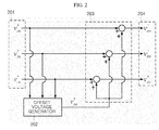
- FIG. 2 shows a process of generating a three-phase pole voltage signal by a pole voltage signal generator in the PWM control unit 104 in the related art.
- the pole-voltage signal generator in the PWM control unit 104 adds three phase-voltage signals 201 including a first phase-voltage signal V * as , a second phase-voltage signal V * bs and a third phase-voltage signal V * cs to an offset voltage V * sn generated in an offset voltage generator 202, respectively, thereby generating three-phase pole-voltage signals 203 including a first pole-voltage signal V * an , a second pole-voltage signal V * bn and a third pole-voltage signal V * cn .
- the offset voltage V * sn is a component that commonly exists in the pole-voltage signals 203, and is a zero sequence voltage such that it does not affect the combination of phase-to-phase voltages.
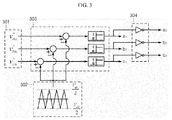
- FIG. 3 shows a process that a control signal generator in the PWM control unit 104 generates a control signal for switching elements by using three-phase pole-voltage signals in the related art.
- the pole-voltage signals 301 generated via the process of FIG. 2 i.e., the first pole-voltage signal V * an , the second pole-voltage signal V * bn and the third pole-voltage signal V * cn are compared with a carrier wave 302 as shown in FIG. 3 .
- the carrier wave 302 shown in FIG. 3 is a triangular carrier wave, other types of carrier waves may also be used depending on the modulation scheme.
- the frequency of the carrier wave 302 is equal to the switching frequency.
- the peak has the maximum value of V dc /2 and the minimum value of -V dc /2.
- the difference between each of the pole-voltage signals 201 and the carrier wave 302 is calculated, and the value of 1 is output if the difference is equal to or greater than 0, and the value of 0 is output if the difference is less than 0 (as indicated by reference numeral 303). Accordingly, an on-signal is output to the switching elements a1, b1 and c1 if the difference between each of the pole-voltage signals 201 and the carrier wave 302 is greater than 0, and an on-signal is output to the switching elements a2, b2 and c2 if the difference between each of the pole-voltage signals 201 and the carrier wave 302 is less than 0 by NOT gates 304.
- the modulation mode is finally determined based on the offset voltage V * sn generated in the offset voltage generator 202.
- the space vector PWM (SVPWM) expressed in Equation 3 is a continuous modulation scheme in which control signals for all of the switching elements are changed for a cycle of a carrier wave.
- a control signal for a switching element in a phase does not change, in order to reduce switching loss.
- One of the most commonly used discontinuous voltage modulation scheme is 60° discontinuous PWM (DPWM), in which switching discontinuous periods of 60° exist around the peak of a phase-voltage signal.
- the discontinuous modulation interval is always set to 120° of a cycle of a reference wave. Accordingly, when the modulation index MI is low, the THD in the output current is very large in the discontinuous modulation mode. As a result, there is another problem in the modulation index by which discontinuous modulation starts is restricted in order to reduce switching loss.
- the offset voltage is continuously generated even in a period where the offset voltage is not necessary and introduced into the inverter via the PWM control unit 104.
- the offset voltage is zero sequence voltage and may result in reduction in the power efficiency or malfunction of a load connected to the inverter. For example, if such zero sequence voltage is applied to an ESS using a grid connected inverter or a photovoltaic module, leakage current may be generated such that power efficiency may be reduced.
- leakage current may be generated such that power efficiency may be reduced.
- torque in the axial direction or bearing current becomes large, possibly causing dielectric breakdown.
- an offset voltage generator and a method for generating an offset voltage of a three-phase inverter that allow voltage modulation mode of the three-phase inverter to switch from a continuous modulation mode to a discontinuous modulation mode without additionally calculating another offset voltage.
- an offset voltage having the minimum RMS is generated to be introduced into the inverter and thus the zero sequence voltage is minimized, thereby preventing reduction in power efficiency and malfunction of a load driven by the inverter.
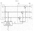
- FIG. 4 is a block diagram of a pole-voltage signal generator included in a PWM control unit 104 according to an exemplary embodiment of the present disclosure.
- the pole-voltage signal generator adds three phase-voltage signals 401 including a first phase-voltage signal V * as , a second phase-voltage signal V * bs and a third phase-voltage signal V * cs to an offset voltage V* sn generated in an offset voltage generator 402, respectively, (as indicated by reference numeral 403), thereby generating three-phase pole-voltage signals 404 including a first pole-voltage signal V * an , a second pole-voltage signal V * bn and a third pole-voltage signal V * c n .
- the offset voltage generator 402 according to the exemplary embodiment of the present disclosure generates an offset voltage V* sn by using phase-voltage signals 401 and a DC link voltage V dc of the three-phase inverter.
- the offset voltage V* sn of the inverter of FIG. 1 has the range as expressed in Equation 5 below: ⁇ V dc 2 ⁇ v min ⁇ v sn * ⁇ V dc 2 ⁇ v max
- V dc 2 ⁇ v max in Equation 5 ⁇ V dc 2 ⁇ v min ⁇ v sn * ⁇ V dc 2 ⁇ v max ⁇ 0 is established. That is, the offset voltage having the minimum absolute value becomes V dc 2 ⁇ v max .
- ⁇ V dc 2 > v min 0 ⁇ ⁇ V dc 2 ⁇ v min ⁇ v sn * ⁇ V dc 2 ⁇ v max is established, such that the offset voltage having the minimum absolute value becomes ⁇ V dc 2 ⁇ v min .
- FIG. 5 is block diagram of the offset voltage generator 402 according to an exemplary embodiment of the present disclosure.
- the offset voltage generator 402 according to the exemplary embodiment of the present disclosure generates the offset voltage V * sn as expressed in Equation 7 in the following manner.
- the offset voltage generator 402 includes a first limiter 502(a), a second limiter 502(b) and a third limiter 502(c) respectively corresponding to the first phase-voltage signal V * as , the second phase-voltage signal V * bs and the third phase-voltage signal V * cs .
- the first limiter 502(a) receives the first phase-voltage signal V * as and compares the received first phase-voltage signal V * as with the maximum limit value and the minimum limit value to output the first limit signal Vas.
- the maximum limit value may be set to V dc 2
- the minimum limit value may be set to ⁇ V dc 2 .
- the first limiter 502(a) outputs the first phase voltage signal V * as as the first limit signal Vas if the first phase voltage signal V * as is equal to or greater than the minimum limit value and equal to or less than the maximum limit value. In addition, the first limiter 502(a) outputs the minimum limit value as the first limit signal Vas if the first phase voltage signal V * as is less than the minimum limit value. In addition, the first limiter 502(a) outputs the maximum limit value as the first limit signal Vas if the first phase voltage signal V * as is greater than the maximum limit value.
- the second limiter 502(b) and the third limiter 502(c) also output the second limit signal Vbs and the third limit signal Vcs, respectively, in the same manner as the first limiter 502(a) described above.
- the 402 outputs, as the offset voltage V * sn , the sum of the difference between the first limit signal Vas and the first phase voltage signal V * as , the difference between the second limit signal Vbs and the second phase voltage signal V * bs , and the difference between the third limit signal Vcs and the third phase voltage signal V * cs , as shown in FIG. 5 .
- the offset voltage V * sn generated by the offset voltage generator 402 becomes 0 if the three phase-voltage signals 501 are between the minimum limit value and the maximum limit value.
- the PWM control unit 104 of FIG. 1 operates in the SPWM mode that is a continuous modulation scheme.
- the pole-voltage signal becomes V dc /2 or -V dc /2, such that the PWM control unit 104 is switched to the discontinuous modulation mode.
- the discontinuous operation range in which the PWM control unit 104 operates in the discontinuous modulation mode is determined by the modulation index MI.
- the voltage modulation mode of the three-phase inverter can be easily switched from the continuous modulation mode to the discontinuous modulation mode without any additional calculating process.
- a discontinuous modulation period is adjusted, such that total harmonic distortion (THD) can be reduced in a period where the modulation index is low compared to the discontinuous modulation scheme in the related art, and switching loss can be reduced in a period where the modulation index is high compared to the continuous modulation scheme in the related art.
- TDD total harmonic distortion
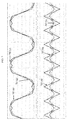
- FIGS. 6 to 8 are graphs for comparing waveforms of offset voltages and pole-voltages according to the PWM control scheme of the present disclosure, the SPWM control scheme in the related art, the SVPWM control scheme in the related art and the 60°DPWM in the related art with one another by varying the modulation index MI.
- the modulation index MI of the PWM control scheme according to the exemplary embodiment of the present disclosure is set to 1.
- FIG. 6 shows a waveform 601(a) of a pole-voltage signal according to the PWM control scheme according to the exemplary embodiment of the present disclosure and the SPWM control scheme in the related art, a waveform 602(a) of a pole-voltage signal according to the SVPWM control scheme in the related art, and a waveform 603(a) of a pole-voltage signal according to the 60°DPWM control scheme in the related art.
- FIG. 6 shows a waveform 601(b) of an offset voltage according to the PWM control scheme according to the exemplary embodiment of the present disclosure and the SPWM control scheme in the related art, a waveform 602(a) of an offset voltage according to the SVPWM control scheme in the related art, and a waveform 603(a) of an offset voltage according to the 60°DPWM control scheme in the related art.
- the PWM control unit 104 operates in the same manner as the SPWM control scheme in the related art if the modulation index MI is set to 1 or less.
- FIG. 7 shows a waveform 701(a) of a pole-voltage signal according to the SPWM control scheme in the related art, a waveform 702(a) of a pole-voltage signal according to the 60°DPWM control scheme in the related art, and a waveform 703(a) of a pole-voltage signal according to the PWM control scheme of the present disclosure.
- FIG. 7 shows a waveform 701(b) of an offset voltage according to the SPWM control scheme in the related art, a waveform 702(b) of an offset voltage according to the 60°DPWM control scheme in the related art, and a waveform 703(b) of an offset voltage according to the PWM control scheme of the present disclosure.
- the discontinuous modulation period according to the PWM control scheme of the present disclosure is longer as the modulation index MI is greater than 1.
- the modulation index MI of the PWM control scheme according to the exemplary embodiment of the present disclosure is set to 2 / 3 .
- FIG. 8 shows a waveform 801(a) of a pole-voltage signal according to the SVPWM control scheme in the related art, and a waveform 802(a) of a pole-voltage signal according to the 60°DPWM control scheme and the PWM control scheme of the present disclosure.
- FIG. 8 shows a waveform 801(b) of an offset voltage according to the SVPWM control scheme in the related art, and a waveform 802(a) of an offset voltage according to the 60°DPWM control scheme and the PWM control scheme of the present disclosure.
- the PWM control unit 104 when the modulation index MI becomes the maximum value of 2 / 3 , the PWM control unit 104 according to the exemplary embodiment of the present disclosure operates in the same manner as in the 60°DPWM control scheme in the related art, such that it has the maximum discontinuous modulation period for a cycle.
- an offset voltage having the minimum absolute value is generated if the modulation index MI is between 1 and the maximum value of 2 / 3 .
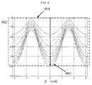
- FIG. 9 is a graph showing a ratio of switching loss in each of the modulation schemes with respect to switching loss in the continuous modulation scheme according to power factor.
- FIG. 9 shows switching loss 901 in the continuous modulation scheme, i.e., the SPWM and SVPWM scheme, and switching loss 903 in the discontinuous modulation scheme, e.g., the 60°DPWM scheme.
- FIG. 9 shows switching loss 902 as the modulation index MI is changed from 1 to 2 / 3 according to the PWM control scheme of the present disclosure.
- the switching loss 902 in the PWM control scheme of the present disclosure is equal to that of the SPWM, i.e., the continuous voltage modulation scheme when the modulation index MI is 1, and the switching loss 902 gradually decreases as the discontinuous modulation period increases if the modulation index MI is greater than 1.
- the switching loss 902 is equal to the switching loss 903 in the 60°DPWM when the modulation index MI is the maximum value of 2 / 3 .
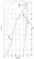
- FIG. 10 is a graph for comparing weighted total harmonic distortion (WTHD) in the continuous modulation scheme and discontinuous modulation scheme in the related art with WTHD in the method for generating offset voltage according to an exemplary embodiment of the present disclosure.
- WTHD weighted total harmonic distortion
- FIG. 10 shows WTHD 1001 in 60°DPWM scheme in the related art, WTHD 1002 in SPWM scheme in the related art, WTHD 1003 in SVPWM scheme in the related art, and WTHD 1004 in PWM control scheme according to an exemplary embodiment of the present disclosure.
- the WTHD 1004 in the PWM control scheme according to the exemplary embodiment of the present disclosure is identical to the WTHD 1002 in the SPWM scheme in the related art when the modulation index MI is equal to or less than the reference index of 1.
- the modulation index MI becomes larger than the reference index of 1
- the discontinuous modulation interval increases, such that the WTHD 1004 gradually increases.
- the WTHD 1004 in PWM scheme according to the exemplary embodiment of the present disclosure increases, it always remains lower than the WTHD 1001 in the 60°DPWM scheme in the related art.
- the PWM control scheme according to the exemplary embodiment of the present disclosure described above is a voltage modulation method in which a zero sequence voltage or an offset voltage calculated using the phase-voltage signals, the limiters and the weight are compared with a triangular wave.
- the smooth switching from the continuous voltage modulation mode to the discontinuous voltage modulation mode can be achieved by adding up differences between phase-voltage signals and respective limit voltage signals after having passed the limiters.
- the discontinuous voltage modulation period can be adjusted by adjusting the maximum limit value and the minimum limit value input to the limiters.
- the PWM control unit operates in the continuous modulation mode when the modulation index is set to a value below the reference index of 1, whereas the PWM control unit is switched to the discontinuous modulation mode when the modulation index becomes larger than the reference index of 1.
- the discontinuous modulation period can be adjusted, such that the THD can be reduced even in a period where the modulation index is low compared to the discontinuous modulation scheme in the related art.
- switching loss can also be reduced in a period where third modulation index is high compared to the continuous modulation scheme in the related art.
- an offset voltage having the minimum RMS is generated to be introduced into the inverter and thus the zero sequence voltage is minimized, thereby preventing reduction in the power efficiency or malfunction of a load driven by the inverter.
Landscapes
- Engineering & Computer Science (AREA)
- Power Engineering (AREA)
- Inverter Devices (AREA)
- Control Of Ac Motors In General (AREA)
- Control Of Eletrric Generators (AREA)
Applications Claiming Priority (1)
| Application Number | Priority Date | Filing Date | Title |
|---|---|---|---|
| KR1020150052598A KR102009512B1 (ko) | 2015-04-14 | 2015-04-14 | 3상 인버터의 옵셋 전압 생성 장치 및 방법 |
Publications (3)
| Publication Number | Publication Date |
|---|---|
| EP3082247A2 true EP3082247A2 (de) | 2016-10-19 |
| EP3082247A3 EP3082247A3 (de) | 2017-01-18 |
| EP3082247B1 EP3082247B1 (de) | 2018-07-25 |
Family
ID=55532215
Family Applications (1)
| Application Number | Title | Priority Date | Filing Date |
|---|---|---|---|
| EP16160443.4A Not-in-force EP3082247B1 (de) | 2015-04-14 | 2016-03-15 | Offsetspannungsgenerator und verfahren zur erzeugung einer offsetspannung eines drehstromwechselrichters |
Country Status (6)
| Country | Link |
|---|---|
| US (1) | US9899936B2 (de) |
| EP (1) | EP3082247B1 (de) |
| JP (1) | JP2016208820A (de) |
| KR (1) | KR102009512B1 (de) |
| CN (1) | CN106059351B (de) |
| ES (1) | ES2685429T3 (de) |
Cited By (3)
| Publication number | Priority date | Publication date | Assignee | Title |
|---|---|---|---|---|
| US10498216B1 (en) | 2018-05-31 | 2019-12-03 | Lsis Co., Ltd. | Device for controlling inverter |
| US20210273594A1 (en) * | 2020-02-27 | 2021-09-02 | Audi Ag | Method for operating a drive device for a motor vehicle, and corresponding drive device |
| KR20240161394A (ko) * | 2023-05-04 | 2024-11-12 | 중앙대학교 산학협력단 | 하이브리드 오프셋 전압을 이용한 삼상 전압원 인버터의 제어 방법 |
Families Citing this family (10)
| Publication number | Priority date | Publication date | Assignee | Title |
|---|---|---|---|---|
| US10833605B2 (en) * | 2016-12-16 | 2020-11-10 | Ge Aviation Systems Llc | Space vector modulation in aerospace applications |
| KR101966318B1 (ko) * | 2017-09-18 | 2019-08-27 | 한국철도기술연구원 | 불연속 변조 기법을 이용한 고속철도 추진제어 장치용 단상 pwm 컨버터 및 그 제어 방법 |
| KR102664500B1 (ko) * | 2019-10-10 | 2024-05-10 | 한국전력공사 | 중전압급 직류전원 공급용 전력변환시스템의 제어 방법 |
| US11456680B2 (en) * | 2020-05-08 | 2022-09-27 | Hamilton Sundstrand Corporation | Over-modulation pulse width modulation with maximum output and minimum harmonics |
| CN112217409B (zh) * | 2020-11-05 | 2024-06-11 | 武汉理工大学 | 三相四桥臂电压型逆变器的变载波脉宽调制系统及方法 |
| HRP20241565T1 (hr) * | 2021-02-05 | 2025-01-17 | Ajax Tocco Magnethermic Corporation | Aktivni ispravljač sa sustavima napajanja izmjenjivača izvora struje i izmjenjivača izvora napona za primjene u indukcijskom grijanju i taljenju |
| EP4210210A1 (de) | 2022-01-08 | 2023-07-12 | Goodrich Aerospace Services Private Limited | Systeme und verfahren für raumvektorpulsbreitemodulationstechnik |
| KR20240037674A (ko) | 2022-09-15 | 2024-03-22 | 현대자동차주식회사 | 인버터 구동 장치 및 이의 제어 방법 |
| KR102570152B1 (ko) * | 2023-03-21 | 2023-08-25 | 주식회사 에코스 | 스위칭 손실을 최소화하는 3상 3-레벨 컨버터를 사용하는 전력 변환 장치 |
| CN119134505B (zh) * | 2024-10-17 | 2025-10-10 | 陕西盛弘电气有限公司 | 三相并网逆变器发波方法、系统、控制器及可读存储介质 |
Family Cites Families (17)
| Publication number | Priority date | Publication date | Assignee | Title |
|---|---|---|---|---|
| JPS6122763A (ja) * | 1984-07-10 | 1986-01-31 | Fanuc Ltd | インバ−タの制御方法 |
| JPS62277064A (ja) * | 1986-05-26 | 1987-12-01 | Mitsubishi Electric Corp | 電圧形アクティブフィルタ装置 |
| JPH0783636B2 (ja) * | 1988-09-06 | 1995-09-06 | 三菱電機株式会社 | Pwmインバータ装置 |
| JP2666641B2 (ja) * | 1991-04-26 | 1997-10-22 | 三菱電機株式会社 | Pwm波形生成方法及びインバータ装置 |
| JP2539146B2 (ja) | 1992-01-24 | 1996-10-02 | 株式会社東芝 | Pwm制御を用いたインバ―タの制御方法及び装置 |
| JP3677804B2 (ja) | 1994-03-10 | 2005-08-03 | 株式会社デンソー | インバータ制御装置 |
| JPH1052062A (ja) | 1996-07-31 | 1998-02-20 | Fuji Electric Co Ltd | 3レベルインバータの制御装置 |
| KR100387758B1 (ko) | 2000-09-23 | 2003-06-18 | 로크웰오토메이션코리아 주식회사 | 전압 변조 방법 |
| JP2005137076A (ja) * | 2003-10-29 | 2005-05-26 | Favess Co Ltd | モータ制御装置及びモータ制御方法 |
| JP4529488B2 (ja) * | 2004-03-05 | 2010-08-25 | 三菱電機株式会社 | 相電圧指令値補正方法およびこの相電圧指令値補正方法を使用したモータ制御装置 |
| JP2007135280A (ja) * | 2005-11-09 | 2007-05-31 | Doshisha | Lcフィルタ付三相pwmインバータの制御方法、及び同方法に従って動作するインバータ装置 |
| JP4561841B2 (ja) * | 2008-02-12 | 2010-10-13 | 株式会社デンソー | 回転機の制御装置、及び回転機の制御システム |
| US8760106B2 (en) * | 2011-03-30 | 2014-06-24 | Bose Corporation | Common mode hysteresis for pulse-width modulation drives |
| US8766588B2 (en) * | 2011-03-30 | 2014-07-01 | Bose Corporation | Rate limited common mode control for pulse-width modulation drives |
| CN103746593A (zh) * | 2013-12-19 | 2014-04-23 | 深圳尚英新能源有限公司 | 基于自然换向的统一pwm调制方法及系统 |
| KR101421017B1 (ko) * | 2014-04-15 | 2014-07-21 | 주식회사 에코스 | 멀티레벨 인버터의 전류 제어 방법 |
| CN104065291B (zh) * | 2014-05-23 | 2016-09-21 | 南京理工大学 | 具有低频振荡抑制功能的中点电压平衡控制系统及方法 |
-
2015
- 2015-04-14 KR KR1020150052598A patent/KR102009512B1/ko not_active Expired - Fee Related
-
2016
- 2016-03-15 EP EP16160443.4A patent/EP3082247B1/de not_active Not-in-force
- 2016-03-15 ES ES16160443.4T patent/ES2685429T3/es active Active
- 2016-04-07 CN CN201610216787.4A patent/CN106059351B/zh not_active Expired - Fee Related
- 2016-04-12 JP JP2016079517A patent/JP2016208820A/ja active Pending
- 2016-04-13 US US15/098,238 patent/US9899936B2/en not_active Expired - Fee Related
Non-Patent Citations (1)
| Title |
|---|
| None |
Cited By (4)
| Publication number | Priority date | Publication date | Assignee | Title |
|---|---|---|---|---|
| US10498216B1 (en) | 2018-05-31 | 2019-12-03 | Lsis Co., Ltd. | Device for controlling inverter |
| EP3576286A1 (de) * | 2018-05-31 | 2019-12-04 | LSIS Co., Ltd. | Vorrichtung zur steuerung eines wechselrichters |
| US20210273594A1 (en) * | 2020-02-27 | 2021-09-02 | Audi Ag | Method for operating a drive device for a motor vehicle, and corresponding drive device |
| KR20240161394A (ko) * | 2023-05-04 | 2024-11-12 | 중앙대학교 산학협력단 | 하이브리드 오프셋 전압을 이용한 삼상 전압원 인버터의 제어 방법 |
Also Published As
| Publication number | Publication date |
|---|---|
| CN106059351A (zh) | 2016-10-26 |
| JP2016208820A (ja) | 2016-12-08 |
| EP3082247A3 (de) | 2017-01-18 |
| US20160308460A1 (en) | 2016-10-20 |
| KR102009512B1 (ko) | 2019-08-13 |
| CN106059351B (zh) | 2019-01-11 |
| EP3082247B1 (de) | 2018-07-25 |
| ES2685429T3 (es) | 2018-10-09 |
| US9899936B2 (en) | 2018-02-20 |
| KR20160122922A (ko) | 2016-10-25 |
Similar Documents
| Publication | Publication Date | Title |
|---|---|---|
| EP3082240B1 (de) | Offsetspannungsgenerator und verfahren zur erzeugung von offsetspannung eines drehstromwechselrichters | |
| EP3082247B1 (de) | Offsetspannungsgenerator und verfahren zur erzeugung einer offsetspannung eines drehstromwechselrichters | |
| US10581361B2 (en) | Multiple inverter system for an electric machine | |
| EP2963799B1 (de) | Verfahren und stromwandlungssystemsteuerungsvorrichtung zur steuerung der igbt-sperrschichttemperatur bei geringer geschwindigkeit | |
| US20070133242A1 (en) | Method and apparatus for controlling voltage linearity of voltage source inverters | |
| EP4213372B1 (de) | Antriebsvorrichtung für motor mit offener wicklung | |
| US20180152123A1 (en) | Adaptive pulse width modulation in motor control systems | |
| EP2634906A2 (de) | Stromquellenleistungswandlungsvorrichtung | |
| US11437921B2 (en) | Direct power converter and control device to improve an input power factor | |
| CN110557042B (zh) | 逆变器的控制装置 | |
| EP2879284A2 (de) | Stromquellenleistungsumwandlungsvorrichtung und Stromquellenleistungsumwandlungsverfahren | |
| US8760106B2 (en) | Common mode hysteresis for pulse-width modulation drives | |
| US11646676B2 (en) | Method and apparatus for generating a three-phase voltage | |
| EA000501B1 (ru) | Способ обработки сигналов с широтно-импульсной модуляцией | |
| JP5972060B2 (ja) | ドライブシステムの制御装置 | |
| US20260095115A1 (en) | AC Motor Control Device | |
| JP2923727B2 (ja) | 電力変換装置 | |
| KR20210029546A (ko) | 파워 변환 장치 및 이의 동작 방법 | |
| RU2556874C1 (ru) | Способ управления автономным инвертором | |
| EP4071998A1 (de) | Pwm-umrichter-steuervorrichtung und steuerverfahren | |
| Mahmood et al. | High speed control of induction machines | |
| KR20250092502A (ko) | 인버터 제어 장치 | |
| Thangaprakash et al. | Performance improvement of Z-source inverter-fed induction motor drives using modified voltage space vector | |
| JPH0739165A (ja) | 電力変換装置 |
Legal Events
| Date | Code | Title | Description |
|---|---|---|---|
| PUAI | Public reference made under article 153(3) epc to a published international application that has entered the european phase |
Free format text: ORIGINAL CODE: 0009012 |
|
| AK | Designated contracting states |
Kind code of ref document: A2 Designated state(s): AL AT BE BG CH CY CZ DE DK EE ES FI FR GB GR HR HU IE IS IT LI LT LU LV MC MK MT NL NO PL PT RO RS SE SI SK SM TR |
|
| AX | Request for extension of the european patent |
Extension state: BA ME |
|
| PUAL | Search report despatched |
Free format text: ORIGINAL CODE: 0009013 |
|
| AK | Designated contracting states |
Kind code of ref document: A3 Designated state(s): AL AT BE BG CH CY CZ DE DK EE ES FI FR GB GR HR HU IE IS IT LI LT LU LV MC MK MT NL NO PL PT RO RS SE SI SK SM TR |
|
| AX | Request for extension of the european patent |
Extension state: BA ME |
|
| RIC1 | Information provided on ipc code assigned before grant |
Ipc: H02M 1/12 20060101ALI20161212BHEP Ipc: H02M 7/5395 20060101ALI20161212BHEP Ipc: H02P 27/08 20060101ALI20161212BHEP Ipc: H02M 7/5387 20070101AFI20161212BHEP |
|
| STAA | Information on the status of an ep patent application or granted ep patent |
Free format text: STATUS: REQUEST FOR EXAMINATION WAS MADE |
|
| 17P | Request for examination filed |
Effective date: 20170607 |
|
| RBV | Designated contracting states (corrected) |
Designated state(s): AL AT BE BG CH CY CZ DE DK EE ES FI FR GB GR HR HU IE IS IT LI LT LU LV MC MK MT NL NO PL PT RO RS SE SI SK SM TR |
|
| GRAP | Despatch of communication of intention to grant a patent |
Free format text: ORIGINAL CODE: EPIDOSNIGR1 |
|
| STAA | Information on the status of an ep patent application or granted ep patent |
Free format text: STATUS: GRANT OF PATENT IS INTENDED |
|
| INTG | Intention to grant announced |
Effective date: 20180503 |
|
| GRAS | Grant fee paid |
Free format text: ORIGINAL CODE: EPIDOSNIGR3 |
|
| GRAA | (expected) grant |
Free format text: ORIGINAL CODE: 0009210 |
|
| STAA | Information on the status of an ep patent application or granted ep patent |
Free format text: STATUS: THE PATENT HAS BEEN GRANTED |
|
| AK | Designated contracting states |
Kind code of ref document: B1 Designated state(s): AL AT BE BG CH CY CZ DE DK EE ES FI FR GB GR HR HU IE IS IT LI LT LU LV MC MK MT NL NO PL PT RO RS SE SI SK SM TR |
|
| REG | Reference to a national code |
Ref country code: GB Ref legal event code: FG4D |
|
| REG | Reference to a national code |
Ref country code: CH Ref legal event code: EP |
|
| REG | Reference to a national code |
Ref country code: AT Ref legal event code: REF Ref document number: 1022841 Country of ref document: AT Kind code of ref document: T Effective date: 20180815 |
|
| REG | Reference to a national code |
Ref country code: IE Ref legal event code: FG4D |
|
| REG | Reference to a national code |
Ref country code: DE Ref legal event code: R096 Ref document number: 602016004194 Country of ref document: DE |
|
| REG | Reference to a national code |
Ref country code: ES Ref legal event code: FG2A Ref document number: 2685429 Country of ref document: ES Kind code of ref document: T3 Effective date: 20181009 |
|
| REG | Reference to a national code |
Ref country code: NL Ref legal event code: MP Effective date: 20180725 |
|
| REG | Reference to a national code |
Ref country code: LT Ref legal event code: MG4D |
|
| PG25 | Lapsed in a contracting state [announced via postgrant information from national office to epo] |
Ref country code: NL Free format text: LAPSE BECAUSE OF FAILURE TO SUBMIT A TRANSLATION OF THE DESCRIPTION OR TO PAY THE FEE WITHIN THE PRESCRIBED TIME-LIMIT Effective date: 20180725 |
|
| REG | Reference to a national code |
Ref country code: AT Ref legal event code: MK05 Ref document number: 1022841 Country of ref document: AT Kind code of ref document: T Effective date: 20180725 |
|
| PG25 | Lapsed in a contracting state [announced via postgrant information from national office to epo] |
Ref country code: BG Free format text: LAPSE BECAUSE OF FAILURE TO SUBMIT A TRANSLATION OF THE DESCRIPTION OR TO PAY THE FEE WITHIN THE PRESCRIBED TIME-LIMIT Effective date: 20181025 Ref country code: LT Free format text: LAPSE BECAUSE OF FAILURE TO SUBMIT A TRANSLATION OF THE DESCRIPTION OR TO PAY THE FEE WITHIN THE PRESCRIBED TIME-LIMIT Effective date: 20180725 Ref country code: PL Free format text: LAPSE BECAUSE OF FAILURE TO SUBMIT A TRANSLATION OF THE DESCRIPTION OR TO PAY THE FEE WITHIN THE PRESCRIBED TIME-LIMIT Effective date: 20180725 Ref country code: IS Free format text: LAPSE BECAUSE OF FAILURE TO SUBMIT A TRANSLATION OF THE DESCRIPTION OR TO PAY THE FEE WITHIN THE PRESCRIBED TIME-LIMIT Effective date: 20181125 Ref country code: RS Free format text: LAPSE BECAUSE OF FAILURE TO SUBMIT A TRANSLATION OF THE DESCRIPTION OR TO PAY THE FEE WITHIN THE PRESCRIBED TIME-LIMIT Effective date: 20180725 Ref country code: SE Free format text: LAPSE BECAUSE OF FAILURE TO SUBMIT A TRANSLATION OF THE DESCRIPTION OR TO PAY THE FEE WITHIN THE PRESCRIBED TIME-LIMIT Effective date: 20180725 Ref country code: AT Free format text: LAPSE BECAUSE OF FAILURE TO SUBMIT A TRANSLATION OF THE DESCRIPTION OR TO PAY THE FEE WITHIN THE PRESCRIBED TIME-LIMIT Effective date: 20180725 Ref country code: GR Free format text: LAPSE BECAUSE OF FAILURE TO SUBMIT A TRANSLATION OF THE DESCRIPTION OR TO PAY THE FEE WITHIN THE PRESCRIBED TIME-LIMIT Effective date: 20181026 Ref country code: NO Free format text: LAPSE BECAUSE OF FAILURE TO SUBMIT A TRANSLATION OF THE DESCRIPTION OR TO PAY THE FEE WITHIN THE PRESCRIBED TIME-LIMIT Effective date: 20181025 Ref country code: FI Free format text: LAPSE BECAUSE OF FAILURE TO SUBMIT A TRANSLATION OF THE DESCRIPTION OR TO PAY THE FEE WITHIN THE PRESCRIBED TIME-LIMIT Effective date: 20180725 |
|
| PG25 | Lapsed in a contracting state [announced via postgrant information from national office to epo] |
Ref country code: HR Free format text: LAPSE BECAUSE OF FAILURE TO SUBMIT A TRANSLATION OF THE DESCRIPTION OR TO PAY THE FEE WITHIN THE PRESCRIBED TIME-LIMIT Effective date: 20180725 Ref country code: AL Free format text: LAPSE BECAUSE OF FAILURE TO SUBMIT A TRANSLATION OF THE DESCRIPTION OR TO PAY THE FEE WITHIN THE PRESCRIBED TIME-LIMIT Effective date: 20180725 Ref country code: LV Free format text: LAPSE BECAUSE OF FAILURE TO SUBMIT A TRANSLATION OF THE DESCRIPTION OR TO PAY THE FEE WITHIN THE PRESCRIBED TIME-LIMIT Effective date: 20180725 |
|
| REG | Reference to a national code |
Ref country code: DE Ref legal event code: R097 Ref document number: 602016004194 Country of ref document: DE |
|
| PG25 | Lapsed in a contracting state [announced via postgrant information from national office to epo] |
Ref country code: EE Free format text: LAPSE BECAUSE OF FAILURE TO SUBMIT A TRANSLATION OF THE DESCRIPTION OR TO PAY THE FEE WITHIN THE PRESCRIBED TIME-LIMIT Effective date: 20180725 Ref country code: RO Free format text: LAPSE BECAUSE OF FAILURE TO SUBMIT A TRANSLATION OF THE DESCRIPTION OR TO PAY THE FEE WITHIN THE PRESCRIBED TIME-LIMIT Effective date: 20180725 Ref country code: CZ Free format text: LAPSE BECAUSE OF FAILURE TO SUBMIT A TRANSLATION OF THE DESCRIPTION OR TO PAY THE FEE WITHIN THE PRESCRIBED TIME-LIMIT Effective date: 20180725 |
|
| PG25 | Lapsed in a contracting state [announced via postgrant information from national office to epo] |
Ref country code: SM Free format text: LAPSE BECAUSE OF FAILURE TO SUBMIT A TRANSLATION OF THE DESCRIPTION OR TO PAY THE FEE WITHIN THE PRESCRIBED TIME-LIMIT Effective date: 20180725 Ref country code: SK Free format text: LAPSE BECAUSE OF FAILURE TO SUBMIT A TRANSLATION OF THE DESCRIPTION OR TO PAY THE FEE WITHIN THE PRESCRIBED TIME-LIMIT Effective date: 20180725 Ref country code: DK Free format text: LAPSE BECAUSE OF FAILURE TO SUBMIT A TRANSLATION OF THE DESCRIPTION OR TO PAY THE FEE WITHIN THE PRESCRIBED TIME-LIMIT Effective date: 20180725 |
|
| PLBE | No opposition filed within time limit |
Free format text: ORIGINAL CODE: 0009261 |
|
| STAA | Information on the status of an ep patent application or granted ep patent |
Free format text: STATUS: NO OPPOSITION FILED WITHIN TIME LIMIT |
|
| 26N | No opposition filed |
Effective date: 20190426 |
|
| PG25 | Lapsed in a contracting state [announced via postgrant information from national office to epo] |
Ref country code: SI Free format text: LAPSE BECAUSE OF FAILURE TO SUBMIT A TRANSLATION OF THE DESCRIPTION OR TO PAY THE FEE WITHIN THE PRESCRIBED TIME-LIMIT Effective date: 20180725 |
|
| PG25 | Lapsed in a contracting state [announced via postgrant information from national office to epo] |
Ref country code: MC Free format text: LAPSE BECAUSE OF FAILURE TO SUBMIT A TRANSLATION OF THE DESCRIPTION OR TO PAY THE FEE WITHIN THE PRESCRIBED TIME-LIMIT Effective date: 20180725 |
|
| REG | Reference to a national code |
Ref country code: CH Ref legal event code: PL |
|
| PG25 | Lapsed in a contracting state [announced via postgrant information from national office to epo] |
Ref country code: LU Free format text: LAPSE BECAUSE OF NON-PAYMENT OF DUE FEES Effective date: 20190315 |
|
| REG | Reference to a national code |
Ref country code: BE Ref legal event code: MM Effective date: 20190331 |
|
| PG25 | Lapsed in a contracting state [announced via postgrant information from national office to epo] |
Ref country code: LI Free format text: LAPSE BECAUSE OF NON-PAYMENT OF DUE FEES Effective date: 20190331 Ref country code: CH Free format text: LAPSE BECAUSE OF NON-PAYMENT OF DUE FEES Effective date: 20190331 Ref country code: IE Free format text: LAPSE BECAUSE OF NON-PAYMENT OF DUE FEES Effective date: 20190315 |
|
| PG25 | Lapsed in a contracting state [announced via postgrant information from national office to epo] |
Ref country code: BE Free format text: LAPSE BECAUSE OF NON-PAYMENT OF DUE FEES Effective date: 20190331 |
|
| PGFP | Annual fee paid to national office [announced via postgrant information from national office to epo] |
Ref country code: FR Payment date: 20191223 Year of fee payment: 5 |
|
| PG25 | Lapsed in a contracting state [announced via postgrant information from national office to epo] |
Ref country code: TR Free format text: LAPSE BECAUSE OF FAILURE TO SUBMIT A TRANSLATION OF THE DESCRIPTION OR TO PAY THE FEE WITHIN THE PRESCRIBED TIME-LIMIT Effective date: 20180725 |
|
| PGFP | Annual fee paid to national office [announced via postgrant information from national office to epo] |
Ref country code: DE Payment date: 20191220 Year of fee payment: 5 Ref country code: GB Payment date: 20200108 Year of fee payment: 5 |
|
| PG25 | Lapsed in a contracting state [announced via postgrant information from national office to epo] |
Ref country code: MT Free format text: LAPSE BECAUSE OF NON-PAYMENT OF DUE FEES Effective date: 20190315 Ref country code: PT Free format text: LAPSE BECAUSE OF FAILURE TO SUBMIT A TRANSLATION OF THE DESCRIPTION OR TO PAY THE FEE WITHIN THE PRESCRIBED TIME-LIMIT Effective date: 20181125 |
|
| PGFP | Annual fee paid to national office [announced via postgrant information from national office to epo] |
Ref country code: ES Payment date: 20200414 Year of fee payment: 5 |
|
| PGFP | Annual fee paid to national office [announced via postgrant information from national office to epo] |
Ref country code: IT Payment date: 20200313 Year of fee payment: 5 |
|
| PG25 | Lapsed in a contracting state [announced via postgrant information from national office to epo] |
Ref country code: CY Free format text: LAPSE BECAUSE OF FAILURE TO SUBMIT A TRANSLATION OF THE DESCRIPTION OR TO PAY THE FEE WITHIN THE PRESCRIBED TIME-LIMIT Effective date: 20180725 |
|
| PG25 | Lapsed in a contracting state [announced via postgrant information from national office to epo] |
Ref country code: HU Free format text: LAPSE BECAUSE OF FAILURE TO SUBMIT A TRANSLATION OF THE DESCRIPTION OR TO PAY THE FEE WITHIN THE PRESCRIBED TIME-LIMIT; INVALID AB INITIO Effective date: 20160315 |
|
| REG | Reference to a national code |
Ref country code: DE Ref legal event code: R119 Ref document number: 602016004194 Country of ref document: DE |
|
| GBPC | Gb: european patent ceased through non-payment of renewal fee |
Effective date: 20210315 |
|
| PG25 | Lapsed in a contracting state [announced via postgrant information from national office to epo] |
Ref country code: FR Free format text: LAPSE BECAUSE OF NON-PAYMENT OF DUE FEES Effective date: 20210331 Ref country code: GB Free format text: LAPSE BECAUSE OF NON-PAYMENT OF DUE FEES Effective date: 20210315 Ref country code: DE Free format text: LAPSE BECAUSE OF NON-PAYMENT OF DUE FEES Effective date: 20211001 |
|
| PG25 | Lapsed in a contracting state [announced via postgrant information from national office to epo] |
Ref country code: IT Free format text: LAPSE BECAUSE OF NON-PAYMENT OF DUE FEES Effective date: 20210315 |
|
| REG | Reference to a national code |
Ref country code: ES Ref legal event code: FD2A Effective date: 20220523 |
|
| PG25 | Lapsed in a contracting state [announced via postgrant information from national office to epo] |
Ref country code: MK Free format text: LAPSE BECAUSE OF FAILURE TO SUBMIT A TRANSLATION OF THE DESCRIPTION OR TO PAY THE FEE WITHIN THE PRESCRIBED TIME-LIMIT Effective date: 20180725 |
|
| PG25 | Lapsed in a contracting state [announced via postgrant information from national office to epo] |
Ref country code: ES Free format text: LAPSE BECAUSE OF NON-PAYMENT OF DUE FEES Effective date: 20210316 |