EP3096454A1 - Comparateur de tension - Google Patents
Comparateur de tension Download PDFInfo
- Publication number
- EP3096454A1 EP3096454A1 EP14891116.7A EP14891116A EP3096454A1 EP 3096454 A1 EP3096454 A1 EP 3096454A1 EP 14891116 A EP14891116 A EP 14891116A EP 3096454 A1 EP3096454 A1 EP 3096454A1
- Authority
- EP
- European Patent Office
- Prior art keywords
- transistor
- drain
- gate
- branch
- source
- Prior art date
- Legal status (The legal status is an assumption and is not a legal conclusion. Google has not performed a legal analysis and makes no representation as to the accuracy of the status listed.)
- Granted
Links
- 230000003068 static effect Effects 0.000 abstract description 12
- 238000010586 diagram Methods 0.000 description 7
- 230000009286 beneficial effect Effects 0.000 description 2
- 230000007812 deficiency Effects 0.000 description 1
- 238000001514 detection method Methods 0.000 description 1
- 238000005516 engineering process Methods 0.000 description 1
- 230000004048 modification Effects 0.000 description 1
- 238000012986 modification Methods 0.000 description 1
- 230000003245 working effect Effects 0.000 description 1
Images




Classifications
-
- H—ELECTRICITY
- H03—ELECTRONIC CIRCUITRY
- H03K—PULSE TECHNIQUE
- H03K5/00—Manipulating of pulses not covered by one of the other main groups of this subclass
- H03K5/22—Circuits having more than one input and one output for comparing pulses or pulse trains with each other according to input signal characteristics, e.g. slope, integral
- H03K5/24—Circuits having more than one input and one output for comparing pulses or pulse trains with each other according to input signal characteristics, e.g. slope, integral the characteristic being amplitude
- H03K5/2472—Circuits having more than one input and one output for comparing pulses or pulse trains with each other according to input signal characteristics, e.g. slope, integral the characteristic being amplitude using field effect transistors
- H03K5/2481—Circuits having more than one input and one output for comparing pulses or pulse trains with each other according to input signal characteristics, e.g. slope, integral the characteristic being amplitude using field effect transistors with at least one differential stage
-
- G—PHYSICS
- G01—MEASURING; TESTING
- G01R—MEASURING ELECTRIC VARIABLES; MEASURING MAGNETIC VARIABLES
- G01R19/00—Arrangements for measuring currents or voltages or for indicating presence or sign thereof
- G01R19/0038—Circuits for comparing several input signals and for indicating the result of this comparison, e.g. equal, different, greater, smaller (comparing pulses or pulse trains according to amplitude)
-
- H—ELECTRICITY
- H03—ELECTRONIC CIRCUITRY
- H03F—AMPLIFIERS
- H03F3/00—Amplifiers with only discharge tubes or only semiconductor devices as amplifying elements
- H03F3/45—Differential amplifiers
- H03F3/45071—Differential amplifiers with semiconductor devices only
-
- H—ELECTRICITY
- H03—ELECTRONIC CIRCUITRY
- H03K—PULSE TECHNIQUE
- H03K5/00—Manipulating of pulses not covered by one of the other main groups of this subclass
- H03K5/22—Circuits having more than one input and one output for comparing pulses or pulse trains with each other according to input signal characteristics, e.g. slope, integral
Definitions
- the present invention relates to electronic fields, and more particularly, relates to a voltage comparator having low static power consumption.
- Low power consumption technologies are more and more concerned in portable electronic devices. For example, with respect to smart phones and tablet computers, static power consumption has become a critical indicator of the products. Because these products use batteries as power supplies, reduction of the power consumption signifies an increase of standby duration and life time, which eventually brings good use experience to users.
- FIG. 1 illustrates a common voltage comparator circuit, and power consumption of the circuit is determined by a tail current source IB.
- the circuit has two deficiencies: firstly, in an equilibrium state where a tested voltage VIN is equal to a voltage of a first input terminal VR, IB is uniformly distributed in a branch where transistors M1 and M2 are located, that is, a current of 0.5*IB is sufficient to support operation of the branch where the transistor M2 is located.
- VIN causes M1 to be cut off
- the IB would totally flow through M2.
- an excessive current of 0.5*IB is wasted.
- the tail current source IB is generally formed by NMOS transistors, and an additional bias circuit is required for providing a gate voltage. Therefore, the actual power consumption of the circuit is even greater.
- a fully-differential high-speed low power consumption comparator in Chinese patent application CN201210242224.4 has the advantages of high output slew rate and high speed. However, the power consumption of such comparator reaches 56 ⁇ W, and this power consumption is calculated without taking the bias circuit needed for the comparator into account. Therefore, the actual power consumption of the circuit is even greater.
- a time domain comparator with a low power consumption feedback control structure in Chinese patent application CN200910242582.3 is characterized by using digital logic control for reducing static power consumption. However, the power consumption of such comparator is 9 ⁇ W, and this power consumption is calculated without taking a digital time sequence circuit needed for the comparator into account. Similarly, the actual power consumption of the circuit is even greater.
- a voltage comparator in Chinese patent application CN201010601379.3 is characterized by using sub-threshold working properties of transistor for reducing the power consumption of the circuit while ensuring a specific circuit delay, and the power consumption is 2 ⁇ W.
- the comparator has four power-consuming branches. Therefore, if it is desired to reduce the operating current to be less than 100 nA, the power consumption of each branch needs to be averagely reduced to 25 nA, and this lowers a reliability of the circuit.
- the present invention is intended to provide a voltage comparator, which requires no additional bias circuit or clock, and further reduces the static power consumption.
- the present invention provides a voltage comparator, including a first branch, a second branch and a third branch; wherein: the first branch includes a first transistor, a second transistor and a third transistor; wherein a source of the first transistor is connected to a power supply, a gate of the first transistor is connected to a drain of the first transistor, and the drain of the first transistor is connected to a drain of the second transistor; a gate of the second transistor is connected to a first input terminal, and a source of the second transistor is connected to a drain of the third transistor; and a source of the third transistor is grounded, and the drain of the third transistor is connected to a gate of the third transistor; the second branch includes a fourth transistor, a fifth transistor and a sixth transistor; wherein a source of the fourth transistor is connected to the power supply, a gate of the fourth transistor is connected to a drain of the fourth transistor, and the drain of the fourth transistor is connected to a drain of the fifth transistor; a gate of the fifth transistor is connected to a second input terminal
- the voltage comparator further includes a first resistor, wherein one terminal of the first resistor is connected to the second input terminal, and the other terminal of the first resistor is grounded.
- the first transistor, the fourth transistor and the seventh transistor are PMOS transistors; and the second transistor, the third transistor, the fifth transistor, the sixth transistor and the eighth transistor are NMOS transistors.
- one terminal of the first resistor is connected to the second input terminal, and the other terminal of the first resistor is connected to the power supply.
- the first transistor, the second transistor, the fourth transistor, the fifth transistor and the seventh transistor are PMOS transistors; and the third transistor, the sixth transistor and the eighth transistor are NMOS transistors.
- An embodiment of the present invention further provides a voltage comparator, including a first branch, a second branch and a third branch; wherein: the first branch includes a first transistor, a second transistor and a third transistor; wherein a source of the first transistor is connected to a power supply, a gate of the first transistor is connected to a drain of the first transistor, and the drain of the first transistor is connected to a drain of the second transistor; a gate of the second transistor is connected to a first input terminal, and a source of the second transistor is connected to a drain of the third transistor; and a source of the third transistor is grounded, and the drain of the third transistor is connected to a gate of the third transistor; the second branch includes a fourth transistor, a fifth transistor and a sixth transistor; wherein a source of the fourth transistor is connected to a power supply, a gate of the fourth transistor is connected to a drain of the fourth transistor, and the drain of the fourth transistor is connected to a drain of the fifth transistor; a gate of the fifth transistor is connected to a second
- the voltage comparator further includes a first resistor, wherein one terminal of the first resistor is connected to the second input terminal, and the other terminal of the first resistor is grounded.
- the first transistor, the fourth transistor and the seventh transistor are PMOS transistors; and the second transistor, the third transistor, the fifth transistor, the sixth transistor and the eighth transistor are NMOS transistors.
- one terminal of the first resistor is connected to the second input terminal, and the other terminal of the first resistor is connected to the power supply.
- the first transistor, the fourth transistor and the seventh transistor are PMOS transistors; and the second transistor, the third transistor, the fifth transistor, the sixth transistor and the eighth transistor are NMOS transistors.
- An embodiment of the present invention further provides a voltage comparator, including a first branch, a second branch, a third branch and a fourth branch; wherein; the first branch includes a first transistor, a second transistor and a third transistor; wherein a source of the first transistor is connected to a power supply, a gate of the first transistor is connected to a drain of the first transistor, and the drain of the first transistor is connected to a drain of the second transistor; a gate of the second transistor is connected to a first input terminal, and a source of the second transistor is connected to a drain of the third transistor; and a source of the third transistor is grounded, and the drain of the third transistor is connected to a gate of the third transistor; the second branch includes a fourth transistor, a fifth transistor and a sixth transistor; wherein a source of the fourth transistor is connected to a power supply, a gate of the fourth transistor is connected to a drain of the fourth transistor, and the drain of the fourth transistor is connected to a drain of the fifth transistor; a gate of the fifth transistor is
- the voltage comparator further includes a first resistor, wherein one terminal of the first resistor is connected to the second input terminal, and the other terminal of the first resistor is grounded.
- the first transistor, the fourth transistor, the seventh transistor and the ninth transistor are PMOS transistors; and the second transistor, the third transistor, the fifth transistor, the sixth transistor, the eighth transistor and the tenth transistor are NMOS transistors.
- one terminal of the first resistor is connected to the second input terminal, and the other terminal of the first resistor is connected to the power supply.
- the first transistor, the second transistor, the fourth transistor, the fifth transistor, the seventh transistor and the ninth transistor are PMOS transistors; and the third transistor, the sixth transistor, the eighth transistor and the tenth transistor are NMOS transistors.
- the voltage comparator As compared with the related art, the voltage comparator according to the embodiments of the present invention has the following beneficial effects: firstly, the circuit has self-biasing capabilities, and thus requires no dedicated bias circuit; secondly, under the same power voltage, the static power consumption of the voltage comparator is relatively low; thirdly, fewer power consuming branches exist in the circuit, and the reliability is high under low power consumption.
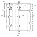
- the present invention provides a voltage comparator, including a first branch A1, a second branch A2 and a third branch A3.
- the first branch A1 includes a first transistor M1, a second transistor M2 and a third transistor M3.
- a source of the first transistor M1 is connected to a power supply VDD
- a gate of the first transistor M1 is connected to a drain of the first transistor M1
- the drain of the first transistor M1 is connected to a drain of the second transistor M2.
- a gate of the second transistor M2 is connected to a first input terminal VR
- a source of the second transistor M2 is connected to a drain of the third transistor M3.
- a source of the third transistor M3 is connected to a ground VSS, and the drain of the third transistor M3 is connected to a gate of the third transistor M3.
- the first branch A1 has self-biasing capability, and requires no external bias signal to control the current thereof.
- the current of the first branch A1 is positively proportional to VR because a higher VR indicates a smaller conduction resistance of the second transistor M2 and a greater current of the first branch A1.
- the second branch A2 includes a fourth transistor M4, a fifth transistor M5 and a sixth transistor M6.
- a source of the fourth transistor M4 is connected to the power supply VDD, a gate of the fourth transistor M4 is connected to a drain of the fourth transistor M4, and the drain of the fourth transistor M4 is connected to a drain of the fifth transistor M5.
- a gate of the fifth transistor M5 is connected to a second input terminal VIN, and a source of the fifth transistor M5 is connected to a drain of the sixth transistor M6.
- a source of the sixth transistor M6 is connected to the ground VSS, and the drain of the sixth transistor M6 is connected to a gate of the sixth transistor M6.
- the first branch A2 also has self-biasing capability, and a current thereof is positively proportional to the VIN.
- the third branch A3 includes a seventh transistor M7 and an eighth transistor M8.
- a source of the seventh transistor M7 is connected to the power supply VDD, a gate of the seventh transistor M7 is connected to a node between the first transistor M1 and the second transistor M2, a drain of the seventh transistor M7 is connected to an output terminal VO of the voltage comparator and a drain of the eighth transistor M8; the seventh transistor M7 and the first transistor M1 form a current mirror.
- a gate of the eighth transistor M8 is connected to a node between the fifth transistor M5 and the sixth transistor M6, the drain of the eighth transistor M8 is connected to the output terminal VO of the voltage comparator, a source of the eighth transistor M8 is connected to the ground VSS; the eighth transistor M8 and the sixth transistor M6 form a current mirror.
- the voltage comparator further includes a first resistor R1, one terminal of the first resistor R1 is connected to the second input terminal VIN, and the other terminal of the first resistor is connected to the ground VSS.
- the first resistor R1 is configured to pull VIN down to 0 V when the second input terminal VIN is floated.
- the first transistor M1, the fourth transistor M4 and the seventh transistor M7 are PMOS transistors; and the second transistor M2, the third transistor M3, the fifth transistor M5, the sixth transistor M6 and the eighth transistor M8 are NMOS transistors.
- the power consumption of the first branch A1 may be desired to be less than 80 nA by designing the voltage value of VR and size designs of M2, M4 and M6.
- the first transistor M1 If the voltage of VIN is 0, the first transistor M1 is cut off, and the current of the second branch A2 is 0. If VIN is floated, the first resistor R1 pulls VIN down to 0 V, and the current of the second branch A2 is still 0. When VIN > 0, the first resistor R1 consumes current from VIN, and when VIN enabled MI to be conducted, the current consumed by the second branch A2 is positively proportional to VIN.
- the voltage comparator may have a lowest static power consumption of less than 0.2 ⁇ W.
- the voltage comparator having the extremely low static power consumption is applied in power voltage detection of a portable electronic device, VR is connected to a battery power supply, and VIN is connected to an external power supply.
- the external power supply when the external power supply is not connected, only the first branch A1 of the voltage comparator consumes the current, and the power consumption may be less than 0.2 ⁇ W.
- the added power consumption includes the current of the second branch A2, the current of the first resistor R1, and the current on M7 and M8.
- the added power consumption does not consume power of the battery.
- the current flowing through the entire circuit is 320 nA
- the average current flowing through the branch A1 is 80 nA.
- the circuit is in the static state, only the first branch A1 is conducted. Since the first branch A1 employs the self-biasing design, the current of the first branch A1 is still 80 nA, the currents of the other branches are 0, and the static power consumption of the entire circuit is 80 nA*VDD. Under the same VDD, the static power consumption of the circuit according to this embodiment is relatively low. Meanwhile, fewer power-consuming branches exist in the circuit, and the reliability under low power consumption is high.
- the voltage comparator according to this embodiment is different from that in Embodiment 1 in that one end of the first resistor R1 is connected to a second input terminal VIN, and the other end of the first resistor R1 is connected to a power supply VDD.
- the first transistor M1, the second transistor M2, the fourth transistor M4, the fifth transistor M5 and the seventh transistor M7 are PMOS transistors; and the third transistor M3, the sixth transistor M6 and the eighth transistor M8 are NMOS transistors.
- the present invention provides a voltage comparator, including a first branch A1, a second branch A2 and a third branch A3.
- the first branch A1 includes a first transistor M1, a second transistor M2 and a third transistor M3.
- a source of the first transistor M1 is connected to a power supply VDD
- a gate of the first transistor M1 is connected to a drain of the first transistor M1
- the drain of the first transistor M1 is connected to a drain of the second transistor M2.
- a gate of the second transistor M2 is connected to a first input terminal VR
- a source of the second transistor M2 is connected to a drain of the third transistor M3.
- a source of the third transistor M3 is connected to a ground VSS, and the drain of the third transistor M3 is connected to a gate of the third transistor M3.
- the second branch A2 includes a fourth transistor M4, a fifth transistor M5 and a sixth transistor M6.
- a source of the fourth transistor M4 is connected to the power supply VDD, a gate of the fourth transistor M4 is connected to a drain of the fourth transistor M4, and the drain of the fourth transistor M4 is connected to a drain of the fifth transistor M5.
- a gate of the fifth transistor M5 is connected to a second input terminal VIN, and the drain of the fifth transistor M5 is connected to a drain of the sixth transistor M6.
- a source of the sixth transistor M6 is connected to the ground VSS, and the drain of the sixth transistor M6 is connected to a gate of the sixth transistor M6.
- the third branch A3 includes a seventh transistor M7 and an eighth transistor M8.
- a source of the seventh transistor M7 is connected to the power supply VDD, a gate of the seventh transistor M7 is connected to a node between the fourth transistor M4 and the fifth transistor M5, a drain of the seventh transistor M7 is connected to an output terminal VO of the voltage comparator and a drain of the eighth transistor M8; the seventh transistor M7 and the fourth transistor M4 form a current mirror.
- a gate of the eighth transistor M8 is connected to a node between the second transistor M2 and the third transistor M3, the drain of the eighth transistor M8 is connected to the output terminal VO of the voltage comparator, a source of the eighth transistor M8 is grounded; the eighth transistor M8 and the third transistor M3 form a current mirror.
- the voltage comparator further includes a first resistor R1, one end of the first resistor R1 is connected to the second input terminal VIN, and the other end of the first resistor is connected to the ground VSS
- the first transistor M1, the fourth transistor M4 and the seventh transistor M7 are PMOS transistors; and the second transistor M2, the third transistor M3, the fifth transistor M5, the sixth transistor M6 and the eighth transistor M8 are NMOS transistors.
- the voltage comparator according to this embodiment is different from that in Embodiment 1 in that one end of the first resistor R1 is connected to a second input terminal VIN, and the other end of the first resistor R1 is connected to a power supply VDD.
- the first transistor M1, the second transistor M2, the fourth transistor M4, the fifth transistor M5 and the seventh transistor M7 are PMOS transistors; and the third transistor M3, the sixth transistor M6 and the eighth transistor M8 are NMOS transistors.
- the present invention provides a voltage comparator, including a first branch A1, a second branch A2, a third branch A3 and a fourth branch A4.
- the first branch A1 includes a first transistor M1, a second transistor M2 and a third transistor M3.
- a source of the first transistor M1 is connected to a power supply VDD
- a gate of the first transistor M1 is connected to a drain of the first transistor M1
- the drain of the first transistor M1 is connected to a drain of the second transistor M2.
- a gate of the second transistor M2 is connected to a first input terminal VR
- a source of the second transistor M2 is connected to a drain of the third transistor M3.
- a source of the third transistor M3 is connected to a ground VSS, and the drain of the third transistor M3 is connected to a gate of the third transistor M3.
- the second branch A2 includes a fourth transistor M4, a fifth transistor M5 and a sixth transistor M6.
- a source of the fourth transistor M4 is connected to the power supply VDD, a gate of the fourth transistor M4 is connected to a drain of the fourth transistor M4, and the drain of the fourth transistor M4 is connected to a drain of the fifth transistor M5.
- a gate of the fifth transistor M5 is connected to a second input terminal VIN, and a source of the fifth transistor M5 is connected to a drain of the sixth transistor M6.
- a source of the sixth transistor M6 is grounded, and the drain of the sixth transistor M6 is connected to a gate of the sixth transistor M6.
- the third branch A3 includes a seventh transistor M7 and an eighth transistor M8.
- a source of the seventh transistor M7 is connected to the power supply VDD, a gate of the seventh transistor M7 is connected to a node between the first transistor M1 and the second transistor M2, a drain of the seventh transistor M7 is connected to an output terminal VO of the voltage comparator and a drain of the eighth transistor M8; the seventh transistor M7 and the first transistor M1 form a current mirror.
- the drain of the eighth transistor M8 is connected to the output terminal VO of the voltage comparator, a source of the eighth transistor M8 is grounded, and a node between the drains of the seventh transistor M7 and the eighth transistor M8 are configured as the output terminal VO.
- the fourth branch A4 includes a ninth transistor M9 and a tenth transistor M10.
- a source of the ninth transistor M9 is connected to the power supply VDD
- a gate of the ninth transistor M9 is connected to the gate of the fourth transistor M4
- a drain of the ninth transistor M9 is connected to a drain of the tenth transistor M10.
- a gate of the tenth transistor M10 is connected to a gate of the eighth transistor M8, the drain of the tenth transistor M10 is connected to the gate of the tenth transistor M10, and a source of the tenth transistor M10 is grounded VSS.
- the voltage comparator further includes a first resistor R1, one terminal of the first resistor R1 is connected to the second input terminal VIN, and the other terminal of the first resistor is connected to the ground VSS.
- the first transistor M1, the fourth transistor M4, the seventh transistor M7 and the ninth transistor M9 are PMOS transistors; and the second transistor M2, the third transistor M3, the fifth transistor M5, the sixth transistor M6, the eighth transistor M8 and the tenth transistor M10 are NMOS transistors.
- the voltage comparator according to this embodiment is different from that in Embodiment 5 in that one end of the first resistor R1 is connected to a second input terminal VIN, and the other end of the first resistor R1 is connected to a power supply VDD.
- the first transistor M1, the second transistor M2, the fourth transistor M4, the fifth transistor M5, the seventh transistor M7 and the ninth transistor M9 are PMOS transistors; and the third transistor M3, the sixth transistor M6, the eighth transistor M8 and the tenth transistor M10 are NMOS transistors.
- the voltage comparator As compared with the related art, the voltage comparator according to the embodiments of the present invention has the following beneficial effects: firstly, the circuit has self-biasing capabilities, and thus requires no dedicated bias circuit; secondly, under the same power voltage, the static power consumption of the voltage comparator is relatively low; thirdly, fewer power consuming branches exist in the circuit, and the reliability is high under low power consumption.
Landscapes
- Physics & Mathematics (AREA)
- Nonlinear Science (AREA)
- Engineering & Computer Science (AREA)
- Power Engineering (AREA)
- General Physics & Mathematics (AREA)
- Manipulation Of Pulses (AREA)
- Measurement Of Current Or Voltage (AREA)
- Amplifiers (AREA)
- Analogue/Digital Conversion (AREA)
Applications Claiming Priority (2)
| Application Number | Priority Date | Filing Date | Title |
|---|---|---|---|
| CN201410174425.4A CN104158516B (zh) | 2014-04-28 | 2014-04-28 | 电压比较器 |
| PCT/CN2014/088469 WO2015165218A1 (fr) | 2014-04-28 | 2014-10-13 | Comparateur de tension |
Publications (3)
| Publication Number | Publication Date |
|---|---|
| EP3096454A1 true EP3096454A1 (fr) | 2016-11-23 |
| EP3096454A4 EP3096454A4 (fr) | 2018-03-21 |
| EP3096454B1 EP3096454B1 (fr) | 2020-02-26 |
Family
ID=51883944
Family Applications (1)
| Application Number | Title | Priority Date | Filing Date |
|---|---|---|---|
| EP14891116.7A Active EP3096454B1 (fr) | 2014-04-28 | 2014-10-13 | Comparateur de tension |
Country Status (5)
| Country | Link |
|---|---|
| US (1) | US9742387B2 (fr) |
| EP (1) | EP3096454B1 (fr) |
| KR (1) | KR101826456B1 (fr) |
| CN (1) | CN104158516B (fr) |
| WO (1) | WO2015165218A1 (fr) |
Families Citing this family (9)
| Publication number | Priority date | Publication date | Assignee | Title |
|---|---|---|---|---|
| CN109379074A (zh) * | 2018-11-21 | 2019-02-22 | 灿芯半导体(上海)有限公司 | 一种电平转换电路 |
| CN110445482B (zh) * | 2019-08-06 | 2020-11-27 | 电子科技大学 | 一种低功耗高摆率的比较器 |
| CN113364278B (zh) * | 2020-04-08 | 2022-07-12 | 澜起电子科技(昆山)有限公司 | 开关电流源电路及开关电流源快速建立方法 |
| CN114448424B (zh) * | 2022-01-14 | 2023-05-23 | 电子科技大学 | 一种自带偏置的低电压比较器 |
| CN116094501B (zh) | 2022-09-09 | 2025-09-16 | 深圳市汇顶科技股份有限公司 | 基于运放的迟滞比较器和芯片 |
| CN115622534B (zh) * | 2022-12-20 | 2023-03-14 | 苏州贝克微电子股份有限公司 | 一种提高运算放大器阻抗的结构及方法 |
| CN116032217A (zh) * | 2022-12-23 | 2023-04-28 | 上海类比半导体技术有限公司 | 振荡器结构及包括振荡器结构的模数转换系统 |
| CN117278004B (zh) * | 2023-11-21 | 2024-02-06 | 拓尔微电子股份有限公司 | 比较电路 |
| CN117792351A (zh) * | 2023-12-20 | 2024-03-29 | 思瑞浦微电子科技(上海)有限责任公司 | 比较器电路和组合比较器电路 |
Family Cites Families (10)
| Publication number | Priority date | Publication date | Assignee | Title |
|---|---|---|---|---|
| JPS6146613A (ja) * | 1984-08-10 | 1986-03-06 | Nec Corp | レベル検出回路 |
| US4818897A (en) * | 1987-09-25 | 1989-04-04 | Texas Instruments Incorporated | Fast one way amplifier stage |
| JP2002084145A (ja) | 2000-09-08 | 2002-03-22 | Nec Corp | Mos線形トランスコンダクタンスアンプ |
| JP4777861B2 (ja) * | 2006-11-07 | 2011-09-21 | フリースケール セミコンダクター インコーポレイテッド | コンパレータ回路 |
| JP5117950B2 (ja) | 2008-07-18 | 2013-01-16 | ラピスセミコンダクタ株式会社 | データ読出回路及び半導体記憶装置 |
| CN101764613B (zh) * | 2009-12-18 | 2012-05-16 | 清华大学 | 低功耗反馈控制结构的时域比较器 |
| CN102571044A (zh) * | 2010-12-22 | 2012-07-11 | 无锡华润上华半导体有限公司 | 电压比较器 |
| JP5503671B2 (ja) * | 2012-01-30 | 2014-05-28 | 株式会社半導体理工学研究センター | 差動増幅回路 |
| JP2013187695A (ja) * | 2012-03-07 | 2013-09-19 | Sony Corp | コンパレータおよびad変換器 |
| CN102769447A (zh) * | 2012-07-12 | 2012-11-07 | 东南大学 | 全差分高速低功耗比较器 |
-
2014
- 2014-04-28 CN CN201410174425.4A patent/CN104158516B/zh active Active
- 2014-10-13 WO PCT/CN2014/088469 patent/WO2015165218A1/fr not_active Ceased
- 2014-10-13 EP EP14891116.7A patent/EP3096454B1/fr active Active
- 2014-10-13 KR KR1020167018348A patent/KR101826456B1/ko active Active
-
2016
- 2016-07-07 US US15/203,796 patent/US9742387B2/en active Active
Also Published As
| Publication number | Publication date |
|---|---|
| US9742387B2 (en) | 2017-08-22 |
| EP3096454B1 (fr) | 2020-02-26 |
| CN104158516B (zh) | 2017-01-11 |
| US20160315604A1 (en) | 2016-10-27 |
| KR20160096676A (ko) | 2016-08-16 |
| EP3096454A4 (fr) | 2018-03-21 |
| CN104158516A (zh) | 2014-11-19 |
| WO2015165218A1 (fr) | 2015-11-05 |
| KR101826456B1 (ko) | 2018-02-06 |
Similar Documents
| Publication | Publication Date | Title |
|---|---|---|
| US9742387B2 (en) | Voltage comparator | |
| CN103186157B (zh) | 适用于逻辑系统的线性电压调节电路 | |
| CN111610812B (zh) | 一种带隙基准电源产生电路及集成电路 | |
| US8405371B2 (en) | Voltage regulator with ripple compensation | |
| US9236732B2 (en) | Voltage regulator | |
| US8736320B2 (en) | Power-on reset circuit | |
| JP2007026337A (ja) | 電圧レギュレータ | |
| US9964975B1 (en) | Semiconductor devices for sensing voltages | |
| US10191527B2 (en) | Brown-out detector | |
| US8766679B1 (en) | Power on reset (POR) circuit | |
| US10355692B2 (en) | Power source monitoring circuit, power on reset circuit, and semiconductor device | |
| US8319548B2 (en) | Integrated circuit having low power mode voltage regulator | |
| US20150089250A1 (en) | Contention Prevention for Sequenced Power Up of Electronic Systems | |
| CN114144742B (zh) | 跨域功率控制电路 | |
| US10522196B2 (en) | Bandgap with system sleep mode | |
| US20100283445A1 (en) | Integrated circuit having low power mode voltage regulator | |
| CN112448577B (zh) | 一种电阻分压电路 | |
| US20150293547A1 (en) | Voltage-current conversion circuit and power supply circuit | |
| CN108776501B (zh) | Ldo和por的复用电路 | |
| US7230456B2 (en) | Low current consumption detector circuit and applications | |
| TWI654510B (zh) | 偏壓電路 | |
| CN215897701U (zh) | 上电和掉电复位电路及系统芯片 |
Legal Events
| Date | Code | Title | Description |
|---|---|---|---|
| PUAI | Public reference made under article 153(3) epc to a published international application that has entered the european phase |
Free format text: ORIGINAL CODE: 0009012 |
|
| 17P | Request for examination filed |
Effective date: 20160714 |
|
| AK | Designated contracting states |
Kind code of ref document: A1 Designated state(s): AL AT BE BG CH CY CZ DE DK EE ES FI FR GB GR HR HU IE IS IT LI LT LU LV MC MK MT NL NO PL PT RO RS SE SI SK SM TR |
|
| AX | Request for extension of the european patent |
Extension state: BA ME |
|
| DAX | Request for extension of the european patent (deleted) | ||
| RAP1 | Party data changed (applicant data changed or rights of an application transferred) |
Owner name: SHENZHEN GOODIX TECHNOLOGY CO., LTD. |
|
| RIC1 | Information provided on ipc code assigned before grant |
Ipc: H03K 5/24 20060101AFI20171102BHEP |
|
| A4 | Supplementary search report drawn up and despatched |
Effective date: 20180215 |
|
| RIC1 | Information provided on ipc code assigned before grant |
Ipc: H03K 5/24 20060101AFI20180210BHEP |
|
| REG | Reference to a national code |
Ref country code: DE Ref legal event code: R079 Ref document number: 602014061709 Country of ref document: DE Free format text: PREVIOUS MAIN CLASS: H03K0005220000 Ipc: H03K0005240000 |
|
| RIC1 | Information provided on ipc code assigned before grant |
Ipc: H03K 5/22 20060101ALI20190903BHEP Ipc: H03K 5/24 20060101AFI20190903BHEP |
|
| GRAP | Despatch of communication of intention to grant a patent |
Free format text: ORIGINAL CODE: EPIDOSNIGR1 |
|
| STAA | Information on the status of an ep patent application or granted ep patent |
Free format text: STATUS: GRANT OF PATENT IS INTENDED |
|
| INTG | Intention to grant announced |
Effective date: 20191021 |
|
| GRAS | Grant fee paid |
Free format text: ORIGINAL CODE: EPIDOSNIGR3 |
|
| GRAA | (expected) grant |
Free format text: ORIGINAL CODE: 0009210 |
|
| STAA | Information on the status of an ep patent application or granted ep patent |
Free format text: STATUS: THE PATENT HAS BEEN GRANTED |
|
| AK | Designated contracting states |
Kind code of ref document: B1 Designated state(s): AL AT BE BG CH CY CZ DE DK EE ES FI FR GB GR HR HU IE IS IT LI LT LU LV MC MK MT NL NO PL PT RO RS SE SI SK SM TR |
|
| REG | Reference to a national code |
Ref country code: GB Ref legal event code: FG4D |
|
| REG | Reference to a national code |
Ref country code: CH Ref legal event code: EP |
|
| REG | Reference to a national code |
Ref country code: AT Ref legal event code: REF Ref document number: 1238890 Country of ref document: AT Kind code of ref document: T Effective date: 20200315 |
|
| REG | Reference to a national code |
Ref country code: IE Ref legal event code: FG4D |
|
| REG | Reference to a national code |
Ref country code: DE Ref legal event code: R096 Ref document number: 602014061709 Country of ref document: DE |
|
| PG25 | Lapsed in a contracting state [announced via postgrant information from national office to epo] |
Ref country code: FI Free format text: LAPSE BECAUSE OF FAILURE TO SUBMIT A TRANSLATION OF THE DESCRIPTION OR TO PAY THE FEE WITHIN THE PRESCRIBED TIME-LIMIT Effective date: 20200226 Ref country code: RS Free format text: LAPSE BECAUSE OF FAILURE TO SUBMIT A TRANSLATION OF THE DESCRIPTION OR TO PAY THE FEE WITHIN THE PRESCRIBED TIME-LIMIT Effective date: 20200226 Ref country code: NO Free format text: LAPSE BECAUSE OF FAILURE TO SUBMIT A TRANSLATION OF THE DESCRIPTION OR TO PAY THE FEE WITHIN THE PRESCRIBED TIME-LIMIT Effective date: 20200526 |
|
| REG | Reference to a national code |
Ref country code: NL Ref legal event code: MP Effective date: 20200226 |
|
| REG | Reference to a national code |
Ref country code: LT Ref legal event code: MG4D |
|
| PG25 | Lapsed in a contracting state [announced via postgrant information from national office to epo] |
Ref country code: BG Free format text: LAPSE BECAUSE OF FAILURE TO SUBMIT A TRANSLATION OF THE DESCRIPTION OR TO PAY THE FEE WITHIN THE PRESCRIBED TIME-LIMIT Effective date: 20200526 Ref country code: IS Free format text: LAPSE BECAUSE OF FAILURE TO SUBMIT A TRANSLATION OF THE DESCRIPTION OR TO PAY THE FEE WITHIN THE PRESCRIBED TIME-LIMIT Effective date: 20200626 Ref country code: LV Free format text: LAPSE BECAUSE OF FAILURE TO SUBMIT A TRANSLATION OF THE DESCRIPTION OR TO PAY THE FEE WITHIN THE PRESCRIBED TIME-LIMIT Effective date: 20200226 Ref country code: SE Free format text: LAPSE BECAUSE OF FAILURE TO SUBMIT A TRANSLATION OF THE DESCRIPTION OR TO PAY THE FEE WITHIN THE PRESCRIBED TIME-LIMIT Effective date: 20200226 Ref country code: GR Free format text: LAPSE BECAUSE OF FAILURE TO SUBMIT A TRANSLATION OF THE DESCRIPTION OR TO PAY THE FEE WITHIN THE PRESCRIBED TIME-LIMIT Effective date: 20200527 Ref country code: HR Free format text: LAPSE BECAUSE OF FAILURE TO SUBMIT A TRANSLATION OF THE DESCRIPTION OR TO PAY THE FEE WITHIN THE PRESCRIBED TIME-LIMIT Effective date: 20200226 |
|
| PG25 | Lapsed in a contracting state [announced via postgrant information from national office to epo] |
Ref country code: NL Free format text: LAPSE BECAUSE OF FAILURE TO SUBMIT A TRANSLATION OF THE DESCRIPTION OR TO PAY THE FEE WITHIN THE PRESCRIBED TIME-LIMIT Effective date: 20200226 |
|
| PG25 | Lapsed in a contracting state [announced via postgrant information from national office to epo] |
Ref country code: EE Free format text: LAPSE BECAUSE OF FAILURE TO SUBMIT A TRANSLATION OF THE DESCRIPTION OR TO PAY THE FEE WITHIN THE PRESCRIBED TIME-LIMIT Effective date: 20200226 Ref country code: SM Free format text: LAPSE BECAUSE OF FAILURE TO SUBMIT A TRANSLATION OF THE DESCRIPTION OR TO PAY THE FEE WITHIN THE PRESCRIBED TIME-LIMIT Effective date: 20200226 Ref country code: DK Free format text: LAPSE BECAUSE OF FAILURE TO SUBMIT A TRANSLATION OF THE DESCRIPTION OR TO PAY THE FEE WITHIN THE PRESCRIBED TIME-LIMIT Effective date: 20200226 Ref country code: SK Free format text: LAPSE BECAUSE OF FAILURE TO SUBMIT A TRANSLATION OF THE DESCRIPTION OR TO PAY THE FEE WITHIN THE PRESCRIBED TIME-LIMIT Effective date: 20200226 Ref country code: RO Free format text: LAPSE BECAUSE OF FAILURE TO SUBMIT A TRANSLATION OF THE DESCRIPTION OR TO PAY THE FEE WITHIN THE PRESCRIBED TIME-LIMIT Effective date: 20200226 Ref country code: LT Free format text: LAPSE BECAUSE OF FAILURE TO SUBMIT A TRANSLATION OF THE DESCRIPTION OR TO PAY THE FEE WITHIN THE PRESCRIBED TIME-LIMIT Effective date: 20200226 Ref country code: CZ Free format text: LAPSE BECAUSE OF FAILURE TO SUBMIT A TRANSLATION OF THE DESCRIPTION OR TO PAY THE FEE WITHIN THE PRESCRIBED TIME-LIMIT Effective date: 20200226 Ref country code: ES Free format text: LAPSE BECAUSE OF FAILURE TO SUBMIT A TRANSLATION OF THE DESCRIPTION OR TO PAY THE FEE WITHIN THE PRESCRIBED TIME-LIMIT Effective date: 20200226 Ref country code: PT Free format text: LAPSE BECAUSE OF FAILURE TO SUBMIT A TRANSLATION OF THE DESCRIPTION OR TO PAY THE FEE WITHIN THE PRESCRIBED TIME-LIMIT Effective date: 20200719 |
|
| REG | Reference to a national code |
Ref country code: AT Ref legal event code: MK05 Ref document number: 1238890 Country of ref document: AT Kind code of ref document: T Effective date: 20200226 |
|
| REG | Reference to a national code |
Ref country code: DE Ref legal event code: R097 Ref document number: 602014061709 Country of ref document: DE |
|
| PLBE | No opposition filed within time limit |
Free format text: ORIGINAL CODE: 0009261 |
|
| STAA | Information on the status of an ep patent application or granted ep patent |
Free format text: STATUS: NO OPPOSITION FILED WITHIN TIME LIMIT |
|
| PG25 | Lapsed in a contracting state [announced via postgrant information from national office to epo] |
Ref country code: AT Free format text: LAPSE BECAUSE OF FAILURE TO SUBMIT A TRANSLATION OF THE DESCRIPTION OR TO PAY THE FEE WITHIN THE PRESCRIBED TIME-LIMIT Effective date: 20200226 Ref country code: IT Free format text: LAPSE BECAUSE OF FAILURE TO SUBMIT A TRANSLATION OF THE DESCRIPTION OR TO PAY THE FEE WITHIN THE PRESCRIBED TIME-LIMIT Effective date: 20200226 |
|
| 26N | No opposition filed |
Effective date: 20201127 |
|
| PG25 | Lapsed in a contracting state [announced via postgrant information from national office to epo] |
Ref country code: PL Free format text: LAPSE BECAUSE OF FAILURE TO SUBMIT A TRANSLATION OF THE DESCRIPTION OR TO PAY THE FEE WITHIN THE PRESCRIBED TIME-LIMIT Effective date: 20200226 Ref country code: SI Free format text: LAPSE BECAUSE OF FAILURE TO SUBMIT A TRANSLATION OF THE DESCRIPTION OR TO PAY THE FEE WITHIN THE PRESCRIBED TIME-LIMIT Effective date: 20200226 |
|
| REG | Reference to a national code |
Ref country code: CH Ref legal event code: PL |
|
| PG25 | Lapsed in a contracting state [announced via postgrant information from national office to epo] |
Ref country code: MC Free format text: LAPSE BECAUSE OF FAILURE TO SUBMIT A TRANSLATION OF THE DESCRIPTION OR TO PAY THE FEE WITHIN THE PRESCRIBED TIME-LIMIT Effective date: 20200226 Ref country code: LU Free format text: LAPSE BECAUSE OF NON-PAYMENT OF DUE FEES Effective date: 20201013 |
|
| REG | Reference to a national code |
Ref country code: BE Ref legal event code: MM Effective date: 20201031 |
|
| PG25 | Lapsed in a contracting state [announced via postgrant information from national office to epo] |
Ref country code: FR Free format text: LAPSE BECAUSE OF NON-PAYMENT OF DUE FEES Effective date: 20201031 |
|
| PG25 | Lapsed in a contracting state [announced via postgrant information from national office to epo] |
Ref country code: BE Free format text: LAPSE BECAUSE OF NON-PAYMENT OF DUE FEES Effective date: 20201031 Ref country code: CH Free format text: LAPSE BECAUSE OF NON-PAYMENT OF DUE FEES Effective date: 20201031 Ref country code: LI Free format text: LAPSE BECAUSE OF NON-PAYMENT OF DUE FEES Effective date: 20201031 |
|
| PG25 | Lapsed in a contracting state [announced via postgrant information from national office to epo] |
Ref country code: IE Free format text: LAPSE BECAUSE OF NON-PAYMENT OF DUE FEES Effective date: 20201013 |
|
| PG25 | Lapsed in a contracting state [announced via postgrant information from national office to epo] |
Ref country code: TR Free format text: LAPSE BECAUSE OF FAILURE TO SUBMIT A TRANSLATION OF THE DESCRIPTION OR TO PAY THE FEE WITHIN THE PRESCRIBED TIME-LIMIT Effective date: 20200226 Ref country code: MT Free format text: LAPSE BECAUSE OF FAILURE TO SUBMIT A TRANSLATION OF THE DESCRIPTION OR TO PAY THE FEE WITHIN THE PRESCRIBED TIME-LIMIT Effective date: 20200226 Ref country code: CY Free format text: LAPSE BECAUSE OF FAILURE TO SUBMIT A TRANSLATION OF THE DESCRIPTION OR TO PAY THE FEE WITHIN THE PRESCRIBED TIME-LIMIT Effective date: 20200226 |
|
| PG25 | Lapsed in a contracting state [announced via postgrant information from national office to epo] |
Ref country code: MK Free format text: LAPSE BECAUSE OF FAILURE TO SUBMIT A TRANSLATION OF THE DESCRIPTION OR TO PAY THE FEE WITHIN THE PRESCRIBED TIME-LIMIT Effective date: 20200226 Ref country code: AL Free format text: LAPSE BECAUSE OF FAILURE TO SUBMIT A TRANSLATION OF THE DESCRIPTION OR TO PAY THE FEE WITHIN THE PRESCRIBED TIME-LIMIT Effective date: 20200226 |
|
| PGFP | Annual fee paid to national office [announced via postgrant information from national office to epo] |
Ref country code: DE Payment date: 20241021 Year of fee payment: 11 |
|
| PGFP | Annual fee paid to national office [announced via postgrant information from national office to epo] |
Ref country code: GB Payment date: 20241025 Year of fee payment: 11 |