EP3110238A2 - Structure d'ensemble et dispositif électronique muni de celle-ci - Google Patents
Structure d'ensemble et dispositif électronique muni de celle-ci Download PDFInfo
- Publication number
- EP3110238A2 EP3110238A2 EP16175340.5A EP16175340A EP3110238A2 EP 3110238 A2 EP3110238 A2 EP 3110238A2 EP 16175340 A EP16175340 A EP 16175340A EP 3110238 A2 EP3110238 A2 EP 3110238A2
- Authority
- EP
- European Patent Office
- Prior art keywords
- converting module
- power converting
- power
- chip
- circuit board
- Prior art date
- Legal status (The legal status is an assumption and is not a legal conclusion. Google has not performed a legal analysis and makes no representation as to the accuracy of the status listed.)
- Granted
Links
Images



















Classifications
-
- H—ELECTRICITY
- H05—ELECTRIC TECHNIQUES NOT OTHERWISE PROVIDED FOR
- H05K—PRINTED CIRCUITS; CASINGS OR CONSTRUCTIONAL DETAILS OF ELECTRIC APPARATUS; MANUFACTURE OF ASSEMBLAGES OF ELECTRICAL COMPONENTS
- H05K1/00—Printed circuits
- H05K1/02—Details
- H05K1/0213—Electrical arrangements not otherwise provided for
- H05K1/0254—High voltage adaptations; Electrical insulation details; Overvoltage or electrostatic discharge protection ; Arrangements for regulating voltages or for using plural voltages
- H05K1/0262—Arrangements for regulating voltages or for using plural voltages
-
- H—ELECTRICITY
- H05—ELECTRIC TECHNIQUES NOT OTHERWISE PROVIDED FOR
- H05K—PRINTED CIRCUITS; CASINGS OR CONSTRUCTIONAL DETAILS OF ELECTRIC APPARATUS; MANUFACTURE OF ASSEMBLAGES OF ELECTRICAL COMPONENTS
- H05K7/00—Constructional details common to different types of electric apparatus
- H05K7/02—Arrangements of circuit components or wiring on supporting structure
-
- G—PHYSICS
- G06—COMPUTING OR CALCULATING; COUNTING
- G06F—ELECTRIC DIGITAL DATA PROCESSING
- G06F1/00—Details not covered by groups G06F3/00 - G06F13/00 and G06F21/00
- G06F1/16—Constructional details or arrangements
- G06F1/18—Packaging or power distribution
- G06F1/183—Internal mounting support structures, e.g. for supporting printed circuit boards
- G06F1/188—Mounting of power supply units
-
- G—PHYSICS
- G06—COMPUTING OR CALCULATING; COUNTING
- G06F—ELECTRIC DIGITAL DATA PROCESSING
- G06F1/00—Details not covered by groups G06F3/00 - G06F13/00 and G06F21/00
- G06F1/16—Constructional details or arrangements
- G06F1/20—Cooling means
-
- H—ELECTRICITY
- H05—ELECTRIC TECHNIQUES NOT OTHERWISE PROVIDED FOR
- H05K—PRINTED CIRCUITS; CASINGS OR CONSTRUCTIONAL DETAILS OF ELECTRIC APPARATUS; MANUFACTURE OF ASSEMBLAGES OF ELECTRICAL COMPONENTS
- H05K1/00—Printed circuits
- H05K1/02—Details
- H05K1/0213—Electrical arrangements not otherwise provided for
- H05K1/0216—Reduction of cross-talk, noise or electromagnetic interference
- H05K1/0218—Reduction of cross-talk, noise or electromagnetic interference by printed shielding conductors, ground planes or power plane
-
- H—ELECTRICITY
- H05—ELECTRIC TECHNIQUES NOT OTHERWISE PROVIDED FOR
- H05K—PRINTED CIRCUITS; CASINGS OR CONSTRUCTIONAL DETAILS OF ELECTRIC APPARATUS; MANUFACTURE OF ASSEMBLAGES OF ELECTRICAL COMPONENTS
- H05K1/00—Printed circuits
- H05K1/02—Details
- H05K1/14—Structural association of two or more printed circuits
- H05K1/141—One or more single auxiliary printed circuits mounted on a main printed circuit, e.g. modules, adapters
-
- H—ELECTRICITY
- H05—ELECTRIC TECHNIQUES NOT OTHERWISE PROVIDED FOR
- H05K—PRINTED CIRCUITS; CASINGS OR CONSTRUCTIONAL DETAILS OF ELECTRIC APPARATUS; MANUFACTURE OF ASSEMBLAGES OF ELECTRICAL COMPONENTS
- H05K1/00—Printed circuits
- H05K1/18—Printed circuits structurally associated with non-printed electric components
- H05K1/181—Printed circuits structurally associated with non-printed electric components associated with surface mounted components
-
- H—ELECTRICITY
- H05—ELECTRIC TECHNIQUES NOT OTHERWISE PROVIDED FOR
- H05K—PRINTED CIRCUITS; CASINGS OR CONSTRUCTIONAL DETAILS OF ELECTRIC APPARATUS; MANUFACTURE OF ASSEMBLAGES OF ELECTRICAL COMPONENTS
- H05K1/00—Printed circuits
- H05K1/18—Printed circuits structurally associated with non-printed electric components
- H05K1/182—Printed circuits structurally associated with non-printed electric components associated with components mounted in printed circuit boards [PCB], e.g. insert-mounted components [IMC]
-
- H—ELECTRICITY
- H05—ELECTRIC TECHNIQUES NOT OTHERWISE PROVIDED FOR
- H05K—PRINTED CIRCUITS; CASINGS OR CONSTRUCTIONAL DETAILS OF ELECTRIC APPARATUS; MANUFACTURE OF ASSEMBLAGES OF ELECTRICAL COMPONENTS
- H05K7/00—Constructional details common to different types of electric apparatus
- H05K7/02—Arrangements of circuit components or wiring on supporting structure
- H05K7/10—Plug-in assemblages of components, e.g. IC sockets
-
- H—ELECTRICITY
- H05—ELECTRIC TECHNIQUES NOT OTHERWISE PROVIDED FOR
- H05K—PRINTED CIRCUITS; CASINGS OR CONSTRUCTIONAL DETAILS OF ELECTRIC APPARATUS; MANUFACTURE OF ASSEMBLAGES OF ELECTRICAL COMPONENTS
- H05K7/00—Constructional details common to different types of electric apparatus
- H05K7/20—Modifications to facilitate cooling, ventilating, or heating
- H05K7/2039—Modifications to facilitate cooling, ventilating, or heating characterised by the heat transfer by conduction from the heat generating element to a dissipating body
-
- H—ELECTRICITY
- H10—SEMICONDUCTOR DEVICES; ELECTRIC SOLID-STATE DEVICES NOT OTHERWISE PROVIDED FOR
- H10W—GENERIC PACKAGES, INTERCONNECTIONS, CONNECTORS OR OTHER CONSTRUCTIONAL DETAILS OF DEVICES COVERED BY CLASS H10
- H10W42/00—Arrangements for protection of devices
- H10W42/20—Arrangements for protection of devices protecting against electromagnetic or particle radiation, e.g. light, X-rays, gamma-rays or electrons
- H10W42/261—Arrangements for protection of devices protecting against electromagnetic or particle radiation, e.g. light, X-rays, gamma-rays or electrons characterised by their shapes or dispositions
- H10W42/276—Arrangements for protection of devices protecting against electromagnetic or particle radiation, e.g. light, X-rays, gamma-rays or electrons characterised by their shapes or dispositions the arrangements being on an external surface of the package, e.g. on the outer surface of an encapsulation
-
- H—ELECTRICITY
- H05—ELECTRIC TECHNIQUES NOT OTHERWISE PROVIDED FOR
- H05K—PRINTED CIRCUITS; CASINGS OR CONSTRUCTIONAL DETAILS OF ELECTRIC APPARATUS; MANUFACTURE OF ASSEMBLAGES OF ELECTRICAL COMPONENTS
- H05K2201/00—Indexing scheme relating to printed circuits covered by H05K1/00
- H05K2201/10—Details of components or other objects attached to or integrated in a printed circuit board
- H05K2201/10007—Types of components
- H05K2201/10189—Non-printed connector
-
- H—ELECTRICITY
- H05—ELECTRIC TECHNIQUES NOT OTHERWISE PROVIDED FOR
- H05K—PRINTED CIRCUITS; CASINGS OR CONSTRUCTIONAL DETAILS OF ELECTRIC APPARATUS; MANUFACTURE OF ASSEMBLAGES OF ELECTRICAL COMPONENTS
- H05K2201/00—Indexing scheme relating to printed circuits covered by H05K1/00
- H05K2201/10—Details of components or other objects attached to or integrated in a printed circuit board
- H05K2201/10227—Other objects, e.g. metallic pieces
- H05K2201/10325—Sockets, i.e. female type connectors comprising metallic connector elements integrated in, or bonded to a common dielectric support
-
- H—ELECTRICITY
- H05—ELECTRIC TECHNIQUES NOT OTHERWISE PROVIDED FOR
- H05K—PRINTED CIRCUITS; CASINGS OR CONSTRUCTIONAL DETAILS OF ELECTRIC APPARATUS; MANUFACTURE OF ASSEMBLAGES OF ELECTRICAL COMPONENTS
- H05K2201/00—Indexing scheme relating to printed circuits covered by H05K1/00
- H05K2201/10—Details of components or other objects attached to or integrated in a printed circuit board
- H05K2201/10431—Details of mounted components
- H05K2201/10507—Involving several components
- H05K2201/10515—Stacked components
-
- H—ELECTRICITY
- H05—ELECTRIC TECHNIQUES NOT OTHERWISE PROVIDED FOR
- H05K—PRINTED CIRCUITS; CASINGS OR CONSTRUCTIONAL DETAILS OF ELECTRIC APPARATUS; MANUFACTURE OF ASSEMBLAGES OF ELECTRICAL COMPONENTS
- H05K2201/00—Indexing scheme relating to printed circuits covered by H05K1/00
- H05K2201/10—Details of components or other objects attached to or integrated in a printed circuit board
- H05K2201/10431—Details of mounted components
- H05K2201/10507—Involving several components
- H05K2201/1053—Mounted components directly electrically connected to each other, i.e. not via the PCB
-
- H—ELECTRICITY
- H05—ELECTRIC TECHNIQUES NOT OTHERWISE PROVIDED FOR
- H05K—PRINTED CIRCUITS; CASINGS OR CONSTRUCTIONAL DETAILS OF ELECTRIC APPARATUS; MANUFACTURE OF ASSEMBLAGES OF ELECTRICAL COMPONENTS
- H05K2201/00—Indexing scheme relating to printed circuits covered by H05K1/00
- H05K2201/10—Details of components or other objects attached to or integrated in a printed circuit board
- H05K2201/10431—Details of mounted components
- H05K2201/10507—Involving several components
- H05K2201/10545—Related components mounted on both sides of the PCB
-
- H—ELECTRICITY
- H05—ELECTRIC TECHNIQUES NOT OTHERWISE PROVIDED FOR
- H05K—PRINTED CIRCUITS; CASINGS OR CONSTRUCTIONAL DETAILS OF ELECTRIC APPARATUS; MANUFACTURE OF ASSEMBLAGES OF ELECTRICAL COMPONENTS
- H05K3/00—Apparatus or processes for manufacturing printed circuits
- H05K3/36—Assembling printed circuits with other printed circuits
- H05K3/368—Assembling printed circuits with other printed circuits parallel to each other
-
- H—ELECTRICITY
- H10—SEMICONDUCTOR DEVICES; ELECTRIC SOLID-STATE DEVICES NOT OTHERWISE PROVIDED FOR
- H10W—GENERIC PACKAGES, INTERCONNECTIONS, CONNECTORS OR OTHER CONSTRUCTIONAL DETAILS OF DEVICES COVERED BY CLASS H10
- H10W40/00—Arrangements for thermal protection or thermal control
- H10W40/10—Arrangements for heating
-
- H—ELECTRICITY
- H10—SEMICONDUCTOR DEVICES; ELECTRIC SOLID-STATE DEVICES NOT OTHERWISE PROVIDED FOR
- H10W—GENERIC PACKAGES, INTERCONNECTIONS, CONNECTORS OR OTHER CONSTRUCTIONAL DETAILS OF DEVICES COVERED BY CLASS H10
- H10W40/00—Arrangements for thermal protection or thermal control
- H10W40/60—Securing means for detachable heating or cooling arrangements, e.g. clamps
- H10W40/611—Bolts or screws
-
- H—ELECTRICITY
- H10—SEMICONDUCTOR DEVICES; ELECTRIC SOLID-STATE DEVICES NOT OTHERWISE PROVIDED FOR
- H10W—GENERIC PACKAGES, INTERCONNECTIONS, CONNECTORS OR OTHER CONSTRUCTIONAL DETAILS OF DEVICES COVERED BY CLASS H10
- H10W42/00—Arrangements for protection of devices
- H10W42/20—Arrangements for protection of devices protecting against electromagnetic or particle radiation, e.g. light, X-rays, gamma-rays or electrons
-
- H—ELECTRICITY
- H10—SEMICONDUCTOR DEVICES; ELECTRIC SOLID-STATE DEVICES NOT OTHERWISE PROVIDED FOR
- H10W—GENERIC PACKAGES, INTERCONNECTIONS, CONNECTORS OR OTHER CONSTRUCTIONAL DETAILS OF DEVICES COVERED BY CLASS H10
- H10W90/00—Package configurations
-
- H—ELECTRICITY
- H10—SEMICONDUCTOR DEVICES; ELECTRIC SOLID-STATE DEVICES NOT OTHERWISE PROVIDED FOR
- H10W—GENERIC PACKAGES, INTERCONNECTIONS, CONNECTORS OR OTHER CONSTRUCTIONAL DETAILS OF DEVICES COVERED BY CLASS H10
- H10W90/00—Package configurations
- H10W90/701—Package configurations characterised by the relative positions of pads or connectors relative to package parts
- H10W90/721—Package configurations characterised by the relative positions of pads or connectors relative to package parts of bump connectors
- H10W90/722—Package configurations characterised by the relative positions of pads or connectors relative to package parts of bump connectors between stacked chips
-
- Y—GENERAL TAGGING OF NEW TECHNOLOGICAL DEVELOPMENTS; GENERAL TAGGING OF CROSS-SECTIONAL TECHNOLOGIES SPANNING OVER SEVERAL SECTIONS OF THE IPC; TECHNICAL SUBJECTS COVERED BY FORMER USPC CROSS-REFERENCE ART COLLECTIONS [XRACs] AND DIGESTS
- Y02—TECHNOLOGIES OR APPLICATIONS FOR MITIGATION OR ADAPTATION AGAINST CLIMATE CHANGE
- Y02D—CLIMATE CHANGE MITIGATION TECHNOLOGIES IN INFORMATION AND COMMUNICATION TECHNOLOGIES [ICT], I.E. INFORMATION AND COMMUNICATION TECHNOLOGIES AIMING AT THE REDUCTION OF THEIR OWN ENERGY USE
- Y02D10/00—Energy efficient computing, e.g. low power processors, power management or thermal management
Definitions
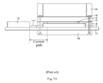
- Fig. 1A is a schematic diagram of a chip installing mode and a power supply mode in prior art.
- a main board 11 of a server is provided with a processor chip 12 (for example, a central processing unit (CPU), a graphics processor unit (GPU), and a data communication switch chip or other large scale integrated circuit chips and the like, here the processor chip in Fig. 1A takes the CPU as an example) and a power supply module 13 (for example, a DC (direct current) /DC module).
- the processor chip 12 is provided thereon with a heat sink 14 for dissipating heat it produces.
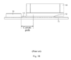
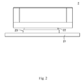
- the present disclosure assembles a power converting module with a circuit board and a chip in a stacking manner, which may shorten a current path between the power converting module and the chip.
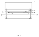
- Fig. 2A is a schematic diagram of an assembly structure for providing power for a chip of another embodiment of the present disclosure.
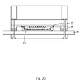
- the chip 22 is electrically connected to the socket 25, the power converting module 23 may be partly buried in the socket 25, a lower surface of the power converting module 23 may be exposed from the socket 25, and the lower surface of the power converting module 23 may contact an upper surface of the circuit board 21.
- the power converting module 23 may be electrically connected to the socket 25.
- the power converting module 23 may provide the second power supply for the chip 22 at least partly through the socket 25.
- the power converting module 23 and the socket 25 may be two separate components to be assembled together, or may be integrated into an undetachable component through molding technology or embedding technology used in packaging. The present disclosure is not limited to this.
- power and/or signals may be transmitted between the chip 22 and the power converting module 23, wherein a transmission direction of the power and/or signals may be as shown by the arrows in Fig. 2E .
- Set positions of the pins electrically connecting the power converting module 23 and the chip 22, connecting mode between the pins and the chip, and structure of the pins may be the same as illustrated in the embodiments as shown in Figs. 2A-2C , which will not be repeated here, but the present disclosure is not limited to this.
- An arrangement of output pins of the power converting module 23 may be determined according to corresponding pin positions of the chip 22, the socket 25 or the circuit board 21, to realize a shorter power and/or signal transmitting distance.
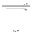
- Figs. 3A and 3B are schematic diagrams of pin arrangements when the power converting module 23 directly connects the chip 22, wherein Fig. 3A is a side view and Fig. 3B is a plan view.
- Power input pins 231 (or electrical energy input terminals) of the chip 22 are denoted by dashed circles, which may be distributed in different regions of surfaces of the chip 22. Power received by respective regions may be different, which is denoted by current values in Fig. 3B .
- Power output pins 232 (denoted by dashed boxes in Fig.
- a part of power input pins 2311 for example, input positive Vin+, input negative Vin-, auxiliary power supply and the like
- a part of signal input pins 2312 for example, input voltage sampling, input current sampling and the like
- a part of signal output pins 2322 for example, an overcurrent warning signal, a module overheat warning signal and the like of the power converting module 23 may be located on the bottom surface of the power converting module 23 and connected with the circuit board 21.
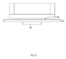
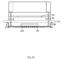
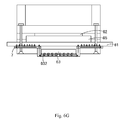
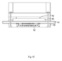
- the power converting module 63 and the back plate 68 may be two components to be used separately or by being combined, or they may be integrated into an undetachable component, for example through molding technology or embedding technology used in packaging to bury the power converting module 63 in the back plate 68.
- the present disclosure is not limited to this.
- a power output and/or signal output may be transmitted from the power converting module 63 to the chip 62 through the circuit board 61 and the socket 65 in sequence.
- the socket may be omitted.
- a connecting mode between the pins 631 and 632 and the circuit board 61 may be welding or pressing.
- a connecting mode between the circuit board 61 and the connector 7 may be welding or pressing, etc.
- a connection between the connector 7 and the circuit board 61 may be by welding.
- the back plate 68 may be used to press the connector 7 on the circuit board 61 and make pins (not shown in Fig. 6E ) between them connected.
- a position at which the connector 7 connects the circuit board 61 may be located on one side or a plurality of sides of the power converting module 63.
- the power output and/or signal output between the power converting module 63 and the circuit board 61 may be transmitted from the power converting module 63 through the pins 632 to the circuit board 61 via the connector 7, as shown by arrows in Figs. 6F-6G .
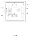
- the input pins 631 and output pins 632 of the power converting module 63 may be located on the same surface (for example, a top surface or a bottom surface) or different surfaces of the power converting module 63.
- the input pins 631 and output pins 632 of the power converting module 63 may be partly located on the same surface and partly located on different surfaces of the power converting module 63.
- the input pins 631 and output pins 632 of the power converting module 63 may adopt the same connecting mode or different connecting modes to connect the circuit board 61 and the chip 62. For example, in Fig.
- a part of power output pins 6321 for example, the output positive Vo+, the output negative Vo-and the like
- a part of signal input pins 6312 for example, the digital communication input and the like
- a part of signal output pins 6322 for example, the digital communication output and the like
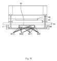
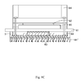
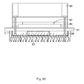
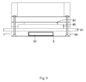
- the connector 7 and the heat sink 64' provided below the power converting module 63 may be separate components, or may be one component or may be molded as a whole, such as a structure as shown in Fig. 8E .
- a process such as stamping, milling and so on, on the connector 7, a wing shaped structure as shown in Fig. 8C is formed on a surface of the connector 7.
- the similar process may be adopted to deal with a structure of the heat sink 64' as shown in Fig. 8D .
- the present disclosure is not limited to this.
- the difference between Figs. 8D and 8C mainly lies in that the back plate 68 is omitted in Fig. 8D .
- Material of the shielding layer may be metal material (such as copper, aluminum and the like) or magnetic material (such as soft magnetic material) correspondingly.
- the shielding layer may be installed as a separate component, or may be integrated together with the power converting module 63 and/or the back plate 68, or may be partly separated and partly integrated with other components. If the back plate 68 is entirely or locally made of metal material, the whole or a part of the metal material of the back plate 68 may be used to realize a function of electromagnetic shielding.
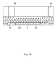
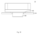
- Fig. 10 is a schematic diagram of stacking of an assembly structure 10 for providing power for a chip according to another embodiment of the present disclosure.
- the power converting module 103 (DC/DC) and the chip 102 is stacked in a vertical direction.
- the power converting module 103 penetrates through an opening in a circuit board 101 and electrically connects the chip 102.
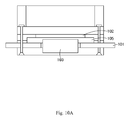
- Fig. 10A is a schematic diagram of stacking of an assembly structure for providing power for a chip according to another embodiment of the present disclosure. It mainly differs from the assembly structure for providing power for a chip as shown in Fig. 10 in that, it further includes a socket 105, and the power converting module 103 may be partly buried in the socket 105. As shown in Fig. 10B , when thickness of the power converting module 103 is less than or equal to that of the circuit board 101, the power converting module 103 may only penetrate through the circuit board 101 and may be not buried in the socket 105.
- the power converting module 103 and the circuit board 101 in Figs. 10 and 10A may be separate elements and may be assembled together later.
- molding technology or embedded technology used in packaging may be adopted to integrate the power converting module 103 and the circuit board 101 into an undetachable component. In one embodiment, the power converting module 103 may be partly buried in the circuit board 101.
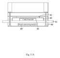
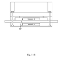
- the control module 69 may not be stacked with the power converting module 69' and the chip 62 and the like, and may be disposed on one side of the circuit board 61.
- the position arrangements of the respective power converting modules 23, 63 and 103 described in the above embodiments are all applicable to the power converting module 69' and/or the control module 69.
- the power converting module 69', the control module 69 and the chip 62 (for example, a CPU) may transmit signals through wireless communication or a wired way, etc. For example, connection and communication may be performed via signal lines (not shown in Fig. 11A ) on the circuit board 61 or the socket 65.
- the power converting modules 23, 63 and 103 may be a DC/DC module, but the present disclosure is not limited to this.
- a part or all of the plurality of modules may locate on the same side of the main board with the chips, or locate on the other sides of the main board, or penetrate through the opening in the main board, or be buried into the main board, or adopt any combination of the above ways.
- Connecting modes between the input and the output of any separate module among the plurality of modules and the system, arrangement and implementation modes of pins of the modules, implementation modes of heat dissipation and anti-interference of the modules may adopt one or more modes described in the above embodiments.
- the arrangement mode of pins of the second module may adopt any one of the above embodiments.
- the CPU may receive power source signal of the first module through pins of the second module, and provide some feedback control signals to the first module.
- signal exchange between the CPU and other chips on the main board may be performed after the socket connects the circuit board, but the present disclosure is not limited thereto.
- the signal exchange may be performed by traces on the surfaces of the second module or inside the second module connecting the main boards 21, 61 and 101.
- the second module may not only serve as a converting module to provide power source for the CPU, but also serve as a connecting structure to electrically connect the CPU and the main board. The present disclosure is not limited to this.
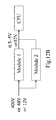
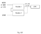
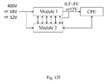
- Figs. 12A-12G are schematic diagrams of several possible functions and mutual connection relationships between two modules.
- Two modules in Fig. 12A constitute a two-stage power supply mode.
- An input voltage of the module 1 is, for example, 400V, 48V or 12V
- an output voltage of the module 2 is, for example, 12V or a range of 0.5V-5V.
- Inputs and outputs of two modules in Fig. 12B are in parallel.
- Two power source modules in Fig. 12C are in the connection relationship of input-series-output-parallel, that is, their inputs are in series and their outputs are in parallel.
- Input ends of two power source modules in Fig. 12D are in parallel, and their outputs supply power for different loads respectively.
- a second module (module 2) and a first module (module 1) in Fig. 12F may communicate with each other.
- a first module in Fig. 12G may be a converting module, whose output is a power with a DC component and a high frequency AC (HFAC) component at the same time.
- a second module in Fig. 12G may be a filter module, which filters the HFAC component output by the first module and transmits the DC power to the chip (CPU).
- a numerical value of an input voltage or output voltage of the power source module or a combination of the power source module may be understood not only as a fixed value, but also as a range containing a given value.
- an input voltage 400V may be understood not only as the input voltage being 400V, but also as a range containing 400V (for example, 200V-500V).
- an input voltage 48V may be understood as a range of 18V-72V
- an input voltage 12V may be understood as a range of 5V-15V
- An output voltage for example, 0.5V-5V, may be understood as that the output voltage is a steady voltage which may be adjusted as needed. The present disclosure is not limited to this.
Landscapes
- Engineering & Computer Science (AREA)
- Microelectronics & Electronic Packaging (AREA)
- Theoretical Computer Science (AREA)
- Physics & Mathematics (AREA)
- Human Computer Interaction (AREA)
- General Engineering & Computer Science (AREA)
- General Physics & Mathematics (AREA)
- Power Engineering (AREA)
- Computer Hardware Design (AREA)
- Electromagnetism (AREA)
- Thermal Sciences (AREA)
- Dc-Dc Converters (AREA)
- Cooling Or The Like Of Semiconductors Or Solid State Devices (AREA)
- Combinations Of Printed Boards (AREA)
- Rectifiers (AREA)
- Inverter Devices (AREA)
Priority Applications (2)
| Application Number | Priority Date | Filing Date | Title |
|---|---|---|---|
| EP21197847.3A EP3986094A3 (fr) | 2015-06-26 | 2016-06-20 | Structure d'ensemble et dispositif électronique muni de celle-ci |
| EP23158349.3A EP4221470A3 (fr) | 2015-06-26 | 2016-06-20 | Structure d'assemblage |
Applications Claiming Priority (1)
| Application Number | Priority Date | Filing Date | Title |
|---|---|---|---|
| CN201510362342.2A CN106332499A (zh) | 2015-06-26 | 2015-06-26 | 一种用于芯片供电的组装结构、电子设备 |
Related Child Applications (3)
| Application Number | Title | Priority Date | Filing Date |
|---|---|---|---|
| EP21197847.3A Division EP3986094A3 (fr) | 2015-06-26 | 2016-06-20 | Structure d'ensemble et dispositif électronique muni de celle-ci |
| EP21197847.3A Division-Into EP3986094A3 (fr) | 2015-06-26 | 2016-06-20 | Structure d'ensemble et dispositif électronique muni de celle-ci |
| EP23158349.3A Division EP4221470A3 (fr) | 2015-06-26 | 2016-06-20 | Structure d'assemblage |
Publications (3)
| Publication Number | Publication Date |
|---|---|
| EP3110238A2 true EP3110238A2 (fr) | 2016-12-28 |
| EP3110238A3 EP3110238A3 (fr) | 2017-04-26 |
| EP3110238B1 EP3110238B1 (fr) | 2021-11-03 |
Family
ID=56235613
Family Applications (3)
| Application Number | Title | Priority Date | Filing Date |
|---|---|---|---|
| EP16175340.5A Active EP3110238B1 (fr) | 2015-06-26 | 2016-06-20 | Structure d'assemblage |
| EP23158349.3A Pending EP4221470A3 (fr) | 2015-06-26 | 2016-06-20 | Structure d'assemblage |
| EP21197847.3A Withdrawn EP3986094A3 (fr) | 2015-06-26 | 2016-06-20 | Structure d'ensemble et dispositif électronique muni de celle-ci |
Family Applications After (2)
| Application Number | Title | Priority Date | Filing Date |
|---|---|---|---|
| EP23158349.3A Pending EP4221470A3 (fr) | 2015-06-26 | 2016-06-20 | Structure d'assemblage |
| EP21197847.3A Withdrawn EP3986094A3 (fr) | 2015-06-26 | 2016-06-20 | Structure d'ensemble et dispositif électronique muni de celle-ci |
Country Status (4)
| Country | Link |
|---|---|
| US (4) | US20160381823A1 (fr) |
| EP (3) | EP3110238B1 (fr) |
| CN (2) | CN106332499A (fr) |
| TW (1) | TWI563376B (fr) |
Cited By (3)
| Publication number | Priority date | Publication date | Assignee | Title |
|---|---|---|---|---|
| CN114520242A (zh) * | 2020-11-20 | 2022-05-20 | 佳能株式会社 | 模块和装备 |
| WO2023110278A1 (fr) * | 2021-12-17 | 2023-06-22 | International Business Machines Corporation | Structure de câble d'interface séparable pour une entrée de puissance sous module haute tension |
| EP4451812A1 (fr) * | 2023-04-21 | 2024-10-23 | Harman Becker Automotive Systems GmbH | Carte de circuit imprimé et son procédé de production |
Families Citing this family (21)
| Publication number | Priority date | Publication date | Assignee | Title |
|---|---|---|---|---|
| WO2018193588A1 (fr) * | 2017-04-20 | 2018-10-25 | 三菱電機株式会社 | Dispositif de conversion de puissance |
| CN109412389B (zh) * | 2017-08-15 | 2020-11-06 | 泰达电子股份有限公司 | 电源转换装置 |
| CN109412390B (zh) * | 2017-08-15 | 2020-09-25 | 泰达电子股份有限公司 | 电源转换装置 |
| CN108107055B (zh) * | 2017-11-20 | 2019-11-15 | 珠海格力电器股份有限公司 | 智能功率模块的控制方法、装置、存储介质和处理器 |
| CN107801362B (zh) * | 2017-11-29 | 2019-11-22 | 北京百度网讯科技有限公司 | 用于数据中心的冷却系统 |
| US10394291B2 (en) * | 2017-11-29 | 2019-08-27 | Facebook, Inc. | Apparatus, system, and method for dissipating heat from expansion components |
| US11183934B2 (en) | 2019-10-17 | 2021-11-23 | Infineon Technologies Americas Corp. | Embedded substrate voltage regulators |
| US11147165B2 (en) * | 2019-10-17 | 2021-10-12 | Infineon Technologies Austria Ag | Electronic system and interposer having an embedded power device module |
| US11071206B2 (en) | 2019-10-17 | 2021-07-20 | Infineon Technologies Austria Ag | Electronic system and processor substrate having an embedded power device module |
| CN113556916B (zh) | 2020-04-26 | 2023-02-28 | 台达电子企业管理(上海)有限公司 | 数据处理装置 |
| CN114079371A (zh) * | 2020-08-18 | 2022-02-22 | 华为技术有限公司 | 电子设备 |
| CN112148081B (zh) * | 2020-09-11 | 2022-06-03 | 北京比特大陆科技有限公司 | 多相交错降压电源和电子设备 |
| CN112349669B (zh) * | 2020-10-26 | 2024-11-29 | 无锡靖芯科技有限公司 | 一种封装集成功率器件的电流采样方法 |
| US12453061B2 (en) | 2022-12-29 | 2025-10-21 | Monolithic Power Systems, Inc. | Sandwich structure power module |
| CN115411956A (zh) * | 2021-05-28 | 2022-11-29 | 华为技术有限公司 | 一种电流传输板、芯片系统及电子设备 |
| US11799374B2 (en) * | 2021-09-16 | 2023-10-24 | International Business Machines Corporation | Vertical power delivery packaging structure |
| US12225665B2 (en) * | 2022-05-05 | 2025-02-11 | Nvidia Corp. | Circuit system and method of manufacturing a printed circuit board |
| CN115912309A (zh) * | 2023-01-10 | 2023-04-04 | 中国科学院微电子研究所 | 一种集群式芯片系统的垂直供配电架构 |
| US12575023B2 (en) * | 2023-03-17 | 2026-03-10 | Infineon Technologies Austria Ag | Voltage regulator module having a power stage |
| CN119440206A (zh) * | 2023-07-28 | 2025-02-14 | 华为技术有限公司 | 供电电路板和计算机设备 |
| WO2025256741A1 (fr) * | 2024-06-13 | 2025-12-18 | Huawei Technologies Co., Ltd. | Ensemble d'alimentation électrique |
Family Cites Families (25)
| Publication number | Priority date | Publication date | Assignee | Title |
|---|---|---|---|---|
| US4636918A (en) * | 1982-07-30 | 1987-01-13 | Rogers Corporation | Decoupled integrated circuit package |
| WO2001065344A2 (fr) * | 2000-02-18 | 2001-09-07 | Incep Technologies, Inc. | Procede et appareil d'alimentation en courant d'un microprocesseur a gestion de chaleur integree et d'interference electromagnetique |
| US6383653B1 (en) * | 2000-02-22 | 2002-05-07 | Moore North America, Inc. | Pressure sensitive cohesive |
| US7952194B2 (en) * | 2001-10-26 | 2011-05-31 | Intel Corporation | Silicon interposer-based hybrid voltage regulator system for VLSI devices |
| KR100596776B1 (ko) * | 2004-01-08 | 2006-07-04 | 주식회사 하이닉스반도체 | 멀티 칩 어셈블리 및 이의 구동 방법 |
| JP4445351B2 (ja) * | 2004-08-31 | 2010-04-07 | 株式会社東芝 | 半導体モジュール |
| US7064955B2 (en) * | 2004-11-24 | 2006-06-20 | Hewlett-Packard Development Company, L.P. | Redundant power for processor circuit board |
| US7280364B2 (en) * | 2004-11-24 | 2007-10-09 | Hewlett-Packard Development Company, L.P. | Apparatus and method for multiprocessor circuit board |
| US7327569B2 (en) * | 2004-12-13 | 2008-02-05 | Hewlett-Packard Development Company, L.P. | Processor module with thermal dissipation device |
| US7791889B2 (en) * | 2005-02-16 | 2010-09-07 | Hewlett-Packard Development Company, L.P. | Redundant power beneath circuit board |
| US7280365B2 (en) * | 2005-02-18 | 2007-10-09 | Hewlett-Packard Development Company, L.P. | Multi-processor module with redundant power |
| US20070013080A1 (en) * | 2005-06-29 | 2007-01-18 | Intel Corporation | Voltage regulators and systems containing same |
| US7402912B2 (en) * | 2005-12-15 | 2008-07-22 | International Business Machines Corporation | Method and power control structure for managing plurality of voltage islands |
| US7778041B2 (en) * | 2006-06-28 | 2010-08-17 | Hon Hai Precision Ind. Co., Ltd. | Interconnection system between CPU and voltage regulator |
| US8498117B2 (en) * | 2006-11-16 | 2013-07-30 | Advanced Micro Devices, Inc. | Variable mount voltage regulator |
| US9147644B2 (en) * | 2008-02-26 | 2015-09-29 | International Rectifier Corporation | Semiconductor device and passive component integration in a semiconductor package |
| US8018738B2 (en) * | 2008-06-02 | 2011-09-13 | Oracle America, Inc., | Voltage regulator attach for high current chip applications |
| US8582333B2 (en) * | 2008-06-30 | 2013-11-12 | Intel Corporation | Integration of switched capacitor networks for power delivery |
| JP5330184B2 (ja) * | 2009-10-06 | 2013-10-30 | 新光電気工業株式会社 | 電子部品装置 |
| US8362606B2 (en) * | 2010-07-29 | 2013-01-29 | Alpha & Omega Semiconductor, Inc. | Wafer level chip scale package |
| US8982563B2 (en) * | 2011-06-28 | 2015-03-17 | Oracle International Corporation | Chip package to support high-frequency processors |
| TW201306685A (zh) * | 2011-07-28 | 2013-02-01 | 金綻科技股份有限公司 | 電路板模組之堆疊 |
| CN102569230A (zh) * | 2012-02-28 | 2012-07-11 | 华为技术有限公司 | 一种半导体器件和电子装置 |
| TWM474236U (zh) * | 2013-07-31 | 2014-03-11 | Delta Electronics Inc | 變壓器結構 |
| DE102014101238A1 (de) * | 2014-01-31 | 2015-08-06 | Hs Elektronik Systeme Gmbh | In Leiterplatten eingebettetes Leistungsmodul |
-
2015
- 2015-06-26 CN CN201510362342.2A patent/CN106332499A/zh active Pending
- 2015-06-26 CN CN201911157050.XA patent/CN111315112A/zh active Pending
- 2015-09-15 TW TW104130496A patent/TWI563376B/zh active
-
2016
- 2016-05-25 US US15/164,214 patent/US20160381823A1/en not_active Abandoned
- 2016-06-20 EP EP16175340.5A patent/EP3110238B1/fr active Active
- 2016-06-20 EP EP23158349.3A patent/EP4221470A3/fr active Pending
- 2016-06-20 EP EP21197847.3A patent/EP3986094A3/fr not_active Withdrawn
-
2020
- 2020-08-27 US US17/004,194 patent/US11503731B2/en active Active
-
2022
- 2022-10-10 US US18/045,180 patent/US12232288B2/en active Active
-
2024
- 2024-12-12 US US18/978,021 patent/US20250113454A1/en active Pending
Non-Patent Citations (1)
| Title |
|---|
| None |
Cited By (4)
| Publication number | Priority date | Publication date | Assignee | Title |
|---|---|---|---|---|
| CN114520242A (zh) * | 2020-11-20 | 2022-05-20 | 佳能株式会社 | 模块和装备 |
| WO2023110278A1 (fr) * | 2021-12-17 | 2023-06-22 | International Business Machines Corporation | Structure de câble d'interface séparable pour une entrée de puissance sous module haute tension |
| US12183999B2 (en) | 2021-12-17 | 2024-12-31 | International Business Machines Corporation | Separable interface cable structure for high voltage under-module power input |
| EP4451812A1 (fr) * | 2023-04-21 | 2024-10-23 | Harman Becker Automotive Systems GmbH | Carte de circuit imprimé et son procédé de production |
Also Published As
| Publication number | Publication date |
|---|---|
| CN111315112A (zh) | 2020-06-19 |
| US20250113454A1 (en) | 2025-04-03 |
| EP4221470A2 (fr) | 2023-08-02 |
| US11503731B2 (en) | 2022-11-15 |
| EP3986094A3 (fr) | 2022-07-20 |
| US20160381823A1 (en) | 2016-12-29 |
| EP3986094A2 (fr) | 2022-04-20 |
| US12232288B2 (en) | 2025-02-18 |
| EP4221470A3 (fr) | 2023-09-13 |
| US20200396855A1 (en) | 2020-12-17 |
| TW201701115A (zh) | 2017-01-01 |
| EP3110238A3 (fr) | 2017-04-26 |
| TWI563376B (en) | 2016-12-21 |
| EP3110238B1 (fr) | 2021-11-03 |
| CN106332499A (zh) | 2017-01-11 |
| US20230059607A1 (en) | 2023-02-23 |
Similar Documents
| Publication | Publication Date | Title |
|---|---|---|
| US11503731B2 (en) | Assembly structure and electronic device having the same | |
| US20220172881A1 (en) | Apparatus | |
| US12088208B1 (en) | Method and apparatus for delivering power to semiconductors | |
| US12058814B2 (en) | Power module and manufacturing method thereof | |
| US11876520B1 (en) | Method and apparatus for delivering power to semiconductors | |
| US9977476B2 (en) | Power supply apparatus | |
| US11320879B2 (en) | Power supply module and electronic device | |
| US10811958B2 (en) | Water-cooling power supply module | |
| US20240171073A1 (en) | Voltage regulator module | |
| US20220254765A1 (en) | Power structure, preparation method, and device | |
| CN111952293A (zh) | 功率模块及其制造方法 | |
| EP3407478B1 (fr) | Dispositif de conversion de puissance | |
| US12453061B2 (en) | Sandwich structure power module | |
| CN108111016A (zh) | 功率模块 | |
| US20260011485A1 (en) | Coupling inductor and power conversion module with same | |
| US20250096209A1 (en) | Double-side-cooling power module | |
| US20260130296A1 (en) | Power module with vertical power paths | |
| US20260066794A1 (en) | Power module for trans-inductor voltage regulator | |
| CN214674915U (zh) | 整流逆变模块及变流器 | |
| CN116825732A (zh) | 一种功率模组和功率转换装置 | |
| JPS628599A (ja) | パワ−モジユ−ル | |
| JPS625697A (ja) | パワ−モジユ−ル |
Legal Events
| Date | Code | Title | Description |
|---|---|---|---|
| PUAI | Public reference made under article 153(3) epc to a published international application that has entered the european phase |
Free format text: ORIGINAL CODE: 0009012 |
|
| STAA | Information on the status of an ep patent application or granted ep patent |
Free format text: STATUS: REQUEST FOR EXAMINATION WAS MADE |
|
| 17P | Request for examination filed |
Effective date: 20160714 |
|
| AK | Designated contracting states |
Kind code of ref document: A2 Designated state(s): AL AT BE BG CH CY CZ DE DK EE ES FI FR GB GR HR HU IE IS IT LI LT LU LV MC MK MT NL NO PL PT RO RS SE SI SK SM TR |
|
| AX | Request for extension of the european patent |
Extension state: BA ME |
|
| RIC1 | Information provided on ipc code assigned before grant |
Ipc: H05K 7/10 20060101ALI20161215BHEP Ipc: G06F 1/18 20060101ALI20161215BHEP Ipc: H05K 1/02 20060101AFI20161215BHEP Ipc: H05K 1/14 20060101ALI20161215BHEP Ipc: H01L 25/065 20060101ALI20161215BHEP |
|
| PUAL | Search report despatched |
Free format text: ORIGINAL CODE: 0009013 |
|
| AK | Designated contracting states |
Kind code of ref document: A3 Designated state(s): AL AT BE BG CH CY CZ DE DK EE ES FI FR GB GR HR HU IE IS IT LI LT LU LV MC MK MT NL NO PL PT RO RS SE SI SK SM TR |
|
| AX | Request for extension of the european patent |
Extension state: BA ME |
|
| RIC1 | Information provided on ipc code assigned before grant |
Ipc: H05K 1/02 20060101AFI20170323BHEP Ipc: H01L 25/065 20060101ALI20170323BHEP Ipc: G06F 1/18 20060101ALI20170323BHEP Ipc: H05K 1/14 20060101ALI20170323BHEP Ipc: H05K 7/10 20060101ALI20170323BHEP |
|
| STAA | Information on the status of an ep patent application or granted ep patent |
Free format text: STATUS: EXAMINATION IS IN PROGRESS |
|
| 17Q | First examination report despatched |
Effective date: 20200925 |
|
| RIC1 | Information provided on ipc code assigned before grant |
Ipc: H01L 25/16 20060101ALN20210402BHEP Ipc: G06F 1/20 20060101ALI20210402BHEP Ipc: G06F 1/18 20060101ALI20210402BHEP Ipc: H05K 7/10 20060101ALI20210402BHEP Ipc: H05K 1/14 20060101ALI20210402BHEP Ipc: H05K 1/02 20060101AFI20210402BHEP |
|
| RIC1 | Information provided on ipc code assigned before grant |
Ipc: H01L 25/16 20060101ALN20210407BHEP Ipc: G06F 1/20 20060101ALI20210407BHEP Ipc: G06F 1/18 20060101ALI20210407BHEP Ipc: H05K 7/10 20060101ALI20210407BHEP Ipc: H05K 1/14 20060101ALI20210407BHEP Ipc: H05K 1/02 20060101AFI20210407BHEP |
|
| GRAP | Despatch of communication of intention to grant a patent |
Free format text: ORIGINAL CODE: EPIDOSNIGR1 |
|
| STAA | Information on the status of an ep patent application or granted ep patent |
Free format text: STATUS: GRANT OF PATENT IS INTENDED |
|
| RIC1 | Information provided on ipc code assigned before grant |
Ipc: H01L 25/16 20060101ALN20210421BHEP Ipc: G06F 1/20 20060101ALI20210421BHEP Ipc: G06F 1/18 20060101ALI20210421BHEP Ipc: H05K 7/10 20060101ALI20210421BHEP Ipc: H05K 1/14 20060101ALI20210421BHEP Ipc: H05K 1/02 20060101AFI20210421BHEP |
|
| INTG | Intention to grant announced |
Effective date: 20210514 |
|
| GRAS | Grant fee paid |
Free format text: ORIGINAL CODE: EPIDOSNIGR3 |
|
| GRAA | (expected) grant |
Free format text: ORIGINAL CODE: 0009210 |
|
| STAA | Information on the status of an ep patent application or granted ep patent |
Free format text: STATUS: THE PATENT HAS BEEN GRANTED |
|
| AK | Designated contracting states |
Kind code of ref document: B1 Designated state(s): AL AT BE BG CH CY CZ DE DK EE ES FI FR GB GR HR HU IE IS IT LI LT LU LV MC MK MT NL NO PL PT RO RS SE SI SK SM TR |
|
| REG | Reference to a national code |
Ref country code: GB Ref legal event code: FG4D |
|
| REG | Reference to a national code |
Ref country code: AT Ref legal event code: REF Ref document number: 1445173 Country of ref document: AT Kind code of ref document: T Effective date: 20211115 Ref country code: CH Ref legal event code: EP |
|
| REG | Reference to a national code |
Ref country code: DE Ref legal event code: R096 Ref document number: 602016065648 Country of ref document: DE |
|
| REG | Reference to a national code |
Ref country code: IE Ref legal event code: FG4D |
|
| REG | Reference to a national code |
Ref country code: NL Ref legal event code: FP |
|
| REG | Reference to a national code |
Ref country code: LT Ref legal event code: MG9D |
|
| REG | Reference to a national code |
Ref country code: AT Ref legal event code: MK05 Ref document number: 1445173 Country of ref document: AT Kind code of ref document: T Effective date: 20211103 |
|
| PG25 | Lapsed in a contracting state [announced via postgrant information from national office to epo] |
Ref country code: RS Free format text: LAPSE BECAUSE OF FAILURE TO SUBMIT A TRANSLATION OF THE DESCRIPTION OR TO PAY THE FEE WITHIN THE PRESCRIBED TIME-LIMIT Effective date: 20211103 Ref country code: LT Free format text: LAPSE BECAUSE OF FAILURE TO SUBMIT A TRANSLATION OF THE DESCRIPTION OR TO PAY THE FEE WITHIN THE PRESCRIBED TIME-LIMIT Effective date: 20211103 Ref country code: FI Free format text: LAPSE BECAUSE OF FAILURE TO SUBMIT A TRANSLATION OF THE DESCRIPTION OR TO PAY THE FEE WITHIN THE PRESCRIBED TIME-LIMIT Effective date: 20211103 Ref country code: BG Free format text: LAPSE BECAUSE OF FAILURE TO SUBMIT A TRANSLATION OF THE DESCRIPTION OR TO PAY THE FEE WITHIN THE PRESCRIBED TIME-LIMIT Effective date: 20220203 Ref country code: AT Free format text: LAPSE BECAUSE OF FAILURE TO SUBMIT A TRANSLATION OF THE DESCRIPTION OR TO PAY THE FEE WITHIN THE PRESCRIBED TIME-LIMIT Effective date: 20211103 |
|
| PG25 | Lapsed in a contracting state [announced via postgrant information from national office to epo] |
Ref country code: IS Free format text: LAPSE BECAUSE OF FAILURE TO SUBMIT A TRANSLATION OF THE DESCRIPTION OR TO PAY THE FEE WITHIN THE PRESCRIBED TIME-LIMIT Effective date: 20220303 Ref country code: SE Free format text: LAPSE BECAUSE OF FAILURE TO SUBMIT A TRANSLATION OF THE DESCRIPTION OR TO PAY THE FEE WITHIN THE PRESCRIBED TIME-LIMIT Effective date: 20211103 Ref country code: PT Free format text: LAPSE BECAUSE OF FAILURE TO SUBMIT A TRANSLATION OF THE DESCRIPTION OR TO PAY THE FEE WITHIN THE PRESCRIBED TIME-LIMIT Effective date: 20220303 Ref country code: PL Free format text: LAPSE BECAUSE OF FAILURE TO SUBMIT A TRANSLATION OF THE DESCRIPTION OR TO PAY THE FEE WITHIN THE PRESCRIBED TIME-LIMIT Effective date: 20211103 Ref country code: NO Free format text: LAPSE BECAUSE OF FAILURE TO SUBMIT A TRANSLATION OF THE DESCRIPTION OR TO PAY THE FEE WITHIN THE PRESCRIBED TIME-LIMIT Effective date: 20220203 Ref country code: LV Free format text: LAPSE BECAUSE OF FAILURE TO SUBMIT A TRANSLATION OF THE DESCRIPTION OR TO PAY THE FEE WITHIN THE PRESCRIBED TIME-LIMIT Effective date: 20211103 Ref country code: HR Free format text: LAPSE BECAUSE OF FAILURE TO SUBMIT A TRANSLATION OF THE DESCRIPTION OR TO PAY THE FEE WITHIN THE PRESCRIBED TIME-LIMIT Effective date: 20211103 Ref country code: GR Free format text: LAPSE BECAUSE OF FAILURE TO SUBMIT A TRANSLATION OF THE DESCRIPTION OR TO PAY THE FEE WITHIN THE PRESCRIBED TIME-LIMIT Effective date: 20220204 Ref country code: ES Free format text: LAPSE BECAUSE OF FAILURE TO SUBMIT A TRANSLATION OF THE DESCRIPTION OR TO PAY THE FEE WITHIN THE PRESCRIBED TIME-LIMIT Effective date: 20211103 |
|
| PG25 | Lapsed in a contracting state [announced via postgrant information from national office to epo] |
Ref country code: SM Free format text: LAPSE BECAUSE OF FAILURE TO SUBMIT A TRANSLATION OF THE DESCRIPTION OR TO PAY THE FEE WITHIN THE PRESCRIBED TIME-LIMIT Effective date: 20211103 Ref country code: SK Free format text: LAPSE BECAUSE OF FAILURE TO SUBMIT A TRANSLATION OF THE DESCRIPTION OR TO PAY THE FEE WITHIN THE PRESCRIBED TIME-LIMIT Effective date: 20211103 Ref country code: RO Free format text: LAPSE BECAUSE OF FAILURE TO SUBMIT A TRANSLATION OF THE DESCRIPTION OR TO PAY THE FEE WITHIN THE PRESCRIBED TIME-LIMIT Effective date: 20211103 Ref country code: EE Free format text: LAPSE BECAUSE OF FAILURE TO SUBMIT A TRANSLATION OF THE DESCRIPTION OR TO PAY THE FEE WITHIN THE PRESCRIBED TIME-LIMIT Effective date: 20211103 Ref country code: DK Free format text: LAPSE BECAUSE OF FAILURE TO SUBMIT A TRANSLATION OF THE DESCRIPTION OR TO PAY THE FEE WITHIN THE PRESCRIBED TIME-LIMIT Effective date: 20211103 Ref country code: CZ Free format text: LAPSE BECAUSE OF FAILURE TO SUBMIT A TRANSLATION OF THE DESCRIPTION OR TO PAY THE FEE WITHIN THE PRESCRIBED TIME-LIMIT Effective date: 20211103 |
|
| REG | Reference to a national code |
Ref country code: DE Ref legal event code: R097 Ref document number: 602016065648 Country of ref document: DE |
|
| PLBE | No opposition filed within time limit |
Free format text: ORIGINAL CODE: 0009261 |
|
| STAA | Information on the status of an ep patent application or granted ep patent |
Free format text: STATUS: NO OPPOSITION FILED WITHIN TIME LIMIT |
|
| 26N | No opposition filed |
Effective date: 20220804 |
|
| PG25 | Lapsed in a contracting state [announced via postgrant information from national office to epo] |
Ref country code: AL Free format text: LAPSE BECAUSE OF FAILURE TO SUBMIT A TRANSLATION OF THE DESCRIPTION OR TO PAY THE FEE WITHIN THE PRESCRIBED TIME-LIMIT Effective date: 20211103 |
|
| PG25 | Lapsed in a contracting state [announced via postgrant information from national office to epo] |
Ref country code: SI Free format text: LAPSE BECAUSE OF FAILURE TO SUBMIT A TRANSLATION OF THE DESCRIPTION OR TO PAY THE FEE WITHIN THE PRESCRIBED TIME-LIMIT Effective date: 20211103 |
|
| PG25 | Lapsed in a contracting state [announced via postgrant information from national office to epo] |
Ref country code: MC Free format text: LAPSE BECAUSE OF FAILURE TO SUBMIT A TRANSLATION OF THE DESCRIPTION OR TO PAY THE FEE WITHIN THE PRESCRIBED TIME-LIMIT Effective date: 20211103 |
|
| REG | Reference to a national code |
Ref country code: CH Ref legal event code: PL |
|
| REG | Reference to a national code |
Ref country code: BE Ref legal event code: MM Effective date: 20220630 |
|
| GBPC | Gb: european patent ceased through non-payment of renewal fee |
Effective date: 20220620 |
|
| PG25 | Lapsed in a contracting state [announced via postgrant information from national office to epo] |
Ref country code: LU Free format text: LAPSE BECAUSE OF NON-PAYMENT OF DUE FEES Effective date: 20220620 Ref country code: LI Free format text: LAPSE BECAUSE OF NON-PAYMENT OF DUE FEES Effective date: 20220630 Ref country code: IE Free format text: LAPSE BECAUSE OF NON-PAYMENT OF DUE FEES Effective date: 20220620 Ref country code: FR Free format text: LAPSE BECAUSE OF NON-PAYMENT OF DUE FEES Effective date: 20220630 Ref country code: CH Free format text: LAPSE BECAUSE OF NON-PAYMENT OF DUE FEES Effective date: 20220630 |
|
| PG25 | Lapsed in a contracting state [announced via postgrant information from national office to epo] |
Ref country code: IT Free format text: LAPSE BECAUSE OF FAILURE TO SUBMIT A TRANSLATION OF THE DESCRIPTION OR TO PAY THE FEE WITHIN THE PRESCRIBED TIME-LIMIT Effective date: 20211103 Ref country code: GB Free format text: LAPSE BECAUSE OF NON-PAYMENT OF DUE FEES Effective date: 20220620 Ref country code: BE Free format text: LAPSE BECAUSE OF NON-PAYMENT OF DUE FEES Effective date: 20220630 |
|
| PG25 | Lapsed in a contracting state [announced via postgrant information from national office to epo] |
Ref country code: HU Free format text: LAPSE BECAUSE OF FAILURE TO SUBMIT A TRANSLATION OF THE DESCRIPTION OR TO PAY THE FEE WITHIN THE PRESCRIBED TIME-LIMIT; INVALID AB INITIO Effective date: 20160620 |
|
| PG25 | Lapsed in a contracting state [announced via postgrant information from national office to epo] |
Ref country code: MK Free format text: LAPSE BECAUSE OF FAILURE TO SUBMIT A TRANSLATION OF THE DESCRIPTION OR TO PAY THE FEE WITHIN THE PRESCRIBED TIME-LIMIT Effective date: 20211103 Ref country code: CY Free format text: LAPSE BECAUSE OF FAILURE TO SUBMIT A TRANSLATION OF THE DESCRIPTION OR TO PAY THE FEE WITHIN THE PRESCRIBED TIME-LIMIT Effective date: 20211103 |
|
| PG25 | Lapsed in a contracting state [announced via postgrant information from national office to epo] |
Ref country code: TR Free format text: LAPSE BECAUSE OF FAILURE TO SUBMIT A TRANSLATION OF THE DESCRIPTION OR TO PAY THE FEE WITHIN THE PRESCRIBED TIME-LIMIT Effective date: 20211103 |
|
| PG25 | Lapsed in a contracting state [announced via postgrant information from national office to epo] |
Ref country code: MT Free format text: LAPSE BECAUSE OF FAILURE TO SUBMIT A TRANSLATION OF THE DESCRIPTION OR TO PAY THE FEE WITHIN THE PRESCRIBED TIME-LIMIT Effective date: 20211103 |
|
| PGFP | Annual fee paid to national office [announced via postgrant information from national office to epo] |
Ref country code: NL Payment date: 20250409 Year of fee payment: 10 |
|
| PGFP | Annual fee paid to national office [announced via postgrant information from national office to epo] |
Ref country code: DE Payment date: 20250402 Year of fee payment: 10 |