EP4451812A1 - Carte de circuit imprimé et son procédé de production - Google Patents
Carte de circuit imprimé et son procédé de production Download PDFInfo
- Publication number
- EP4451812A1 EP4451812A1 EP23169228.6A EP23169228A EP4451812A1 EP 4451812 A1 EP4451812 A1 EP 4451812A1 EP 23169228 A EP23169228 A EP 23169228A EP 4451812 A1 EP4451812 A1 EP 4451812A1
- Authority
- EP
- European Patent Office
- Prior art keywords
- pcb
- thermal
- pad
- thermal pad
- pads
- Prior art date
- Legal status (The legal status is an assumption and is not a legal conclusion. Google has not performed a legal analysis and makes no representation as to the accuracy of the status listed.)
- Pending
Links
Images



Classifications
-
- H—ELECTRICITY
- H05—ELECTRIC TECHNIQUES NOT OTHERWISE PROVIDED FOR
- H05K—PRINTED CIRCUITS; CASINGS OR CONSTRUCTIONAL DETAILS OF ELECTRIC APPARATUS; MANUFACTURE OF ASSEMBLAGES OF ELECTRICAL COMPONENTS
- H05K1/00—Printed circuits
- H05K1/02—Details
- H05K1/11—Printed elements for providing electric connections to or between printed circuits
- H05K1/111—Pads for surface mounting, e.g. lay-out
-
- H—ELECTRICITY
- H05—ELECTRIC TECHNIQUES NOT OTHERWISE PROVIDED FOR
- H05K—PRINTED CIRCUITS; CASINGS OR CONSTRUCTIONAL DETAILS OF ELECTRIC APPARATUS; MANUFACTURE OF ASSEMBLAGES OF ELECTRICAL COMPONENTS
- H05K3/00—Apparatus or processes for manufacturing printed circuits
- H05K3/30—Assembling printed circuits with electric components, e.g. with resistors
- H05K3/32—Assembling printed circuits with electric components, e.g. with resistors electrically connecting electric components or wires to printed circuits
- H05K3/34—Assembling printed circuits with electric components, e.g. with resistors electrically connecting electric components or wires to printed circuits by soldering
- H05K3/341—Surface mounted components
- H05K3/3415—Surface mounted components on both sides of the substrate or combined with lead-in-hole components
-
- H—ELECTRICITY
- H05—ELECTRIC TECHNIQUES NOT OTHERWISE PROVIDED FOR
- H05K—PRINTED CIRCUITS; CASINGS OR CONSTRUCTIONAL DETAILS OF ELECTRIC APPARATUS; MANUFACTURE OF ASSEMBLAGES OF ELECTRICAL COMPONENTS
- H05K1/00—Printed circuits
- H05K1/02—Details
- H05K1/0201—Thermal arrangements, e.g. for cooling, heating or preventing overheating
- H05K1/0203—Cooling of mounted components
- H05K1/0204—Cooling of mounted components using means for thermal conduction connection in the thickness direction of the substrate
- H05K1/0206—Cooling of mounted components using means for thermal conduction connection in the thickness direction of the substrate by printed thermal vias
-
- H—ELECTRICITY
- H05—ELECTRIC TECHNIQUES NOT OTHERWISE PROVIDED FOR
- H05K—PRINTED CIRCUITS; CASINGS OR CONSTRUCTIONAL DETAILS OF ELECTRIC APPARATUS; MANUFACTURE OF ASSEMBLAGES OF ELECTRICAL COMPONENTS
- H05K1/00—Printed circuits
- H05K1/02—Details
-
- H—ELECTRICITY
- H05—ELECTRIC TECHNIQUES NOT OTHERWISE PROVIDED FOR
- H05K—PRINTED CIRCUITS; CASINGS OR CONSTRUCTIONAL DETAILS OF ELECTRIC APPARATUS; MANUFACTURE OF ASSEMBLAGES OF ELECTRICAL COMPONENTS
- H05K1/00—Printed circuits
- H05K1/02—Details
- H05K1/0201—Thermal arrangements, e.g. for cooling, heating or preventing overheating
-
- H—ELECTRICITY
- H05—ELECTRIC TECHNIQUES NOT OTHERWISE PROVIDED FOR
- H05K—PRINTED CIRCUITS; CASINGS OR CONSTRUCTIONAL DETAILS OF ELECTRIC APPARATUS; MANUFACTURE OF ASSEMBLAGES OF ELECTRICAL COMPONENTS
- H05K1/00—Printed circuits
- H05K1/02—Details
- H05K1/0201—Thermal arrangements, e.g. for cooling, heating or preventing overheating
- H05K1/0203—Cooling of mounted components
- H05K1/0207—Cooling of mounted components using internal conductor planes parallel to the surface for thermal conduction, e.g. power planes
-
- H—ELECTRICITY
- H05—ELECTRIC TECHNIQUES NOT OTHERWISE PROVIDED FOR
- H05K—PRINTED CIRCUITS; CASINGS OR CONSTRUCTIONAL DETAILS OF ELECTRIC APPARATUS; MANUFACTURE OF ASSEMBLAGES OF ELECTRICAL COMPONENTS
- H05K1/00—Printed circuits
- H05K1/02—Details
- H05K1/0213—Electrical arrangements not otherwise provided for
- H05K1/0216—Reduction of cross-talk, noise or electromagnetic interference
- H05K1/0218—Reduction of cross-talk, noise or electromagnetic interference by printed shielding conductors, ground planes or power plane
-
- H—ELECTRICITY
- H05—ELECTRIC TECHNIQUES NOT OTHERWISE PROVIDED FOR
- H05K—PRINTED CIRCUITS; CASINGS OR CONSTRUCTIONAL DETAILS OF ELECTRIC APPARATUS; MANUFACTURE OF ASSEMBLAGES OF ELECTRICAL COMPONENTS
- H05K1/00—Printed circuits
- H05K1/02—Details
- H05K1/11—Printed elements for providing electric connections to or between printed circuits
- H05K1/111—Pads for surface mounting, e.g. lay-out
- H05K1/112—Pads for surface mounting, e.g. lay-out directly combined with via connections
-
- H—ELECTRICITY
- H05—ELECTRIC TECHNIQUES NOT OTHERWISE PROVIDED FOR
- H05K—PRINTED CIRCUITS; CASINGS OR CONSTRUCTIONAL DETAILS OF ELECTRIC APPARATUS; MANUFACTURE OF ASSEMBLAGES OF ELECTRICAL COMPONENTS
- H05K1/00—Printed circuits
- H05K1/18—Printed circuits structurally associated with non-printed electric components
- H05K1/181—Printed circuits structurally associated with non-printed electric components associated with surface mounted components
-
- H—ELECTRICITY
- H05—ELECTRIC TECHNIQUES NOT OTHERWISE PROVIDED FOR
- H05K—PRINTED CIRCUITS; CASINGS OR CONSTRUCTIONAL DETAILS OF ELECTRIC APPARATUS; MANUFACTURE OF ASSEMBLAGES OF ELECTRICAL COMPONENTS
- H05K3/00—Apparatus or processes for manufacturing printed circuits
-
- H—ELECTRICITY
- H05—ELECTRIC TECHNIQUES NOT OTHERWISE PROVIDED FOR
- H05K—PRINTED CIRCUITS; CASINGS OR CONSTRUCTIONAL DETAILS OF ELECTRIC APPARATUS; MANUFACTURE OF ASSEMBLAGES OF ELECTRICAL COMPONENTS
- H05K3/00—Apparatus or processes for manufacturing printed circuits
- H05K3/30—Assembling printed circuits with electric components, e.g. with resistors
- H05K3/32—Assembling printed circuits with electric components, e.g. with resistors electrically connecting electric components or wires to printed circuits
-
- H—ELECTRICITY
- H05—ELECTRIC TECHNIQUES NOT OTHERWISE PROVIDED FOR
- H05K—PRINTED CIRCUITS; CASINGS OR CONSTRUCTIONAL DETAILS OF ELECTRIC APPARATUS; MANUFACTURE OF ASSEMBLAGES OF ELECTRICAL COMPONENTS
- H05K3/00—Apparatus or processes for manufacturing printed circuits
- H05K3/40—Forming printed elements for providing electric connections to or between printed circuits
- H05K3/4007—Surface contacts, e.g. bumps
-
- H—ELECTRICITY
- H05—ELECTRIC TECHNIQUES NOT OTHERWISE PROVIDED FOR
- H05K—PRINTED CIRCUITS; CASINGS OR CONSTRUCTIONAL DETAILS OF ELECTRIC APPARATUS; MANUFACTURE OF ASSEMBLAGES OF ELECTRICAL COMPONENTS
- H05K3/00—Apparatus or processes for manufacturing printed circuits
- H05K3/40—Forming printed elements for providing electric connections to or between printed circuits
- H05K3/4038—Through-connections; Vertical interconnect access [VIA] connections
-
- H—ELECTRICITY
- H05—ELECTRIC TECHNIQUES NOT OTHERWISE PROVIDED FOR
- H05K—PRINTED CIRCUITS; CASINGS OR CONSTRUCTIONAL DETAILS OF ELECTRIC APPARATUS; MANUFACTURE OF ASSEMBLAGES OF ELECTRICAL COMPONENTS
- H05K2201/00—Indexing scheme relating to printed circuits covered by H05K1/00
- H05K2201/09—Shape and layout
- H05K2201/09209—Shape and layout details of conductors
- H05K2201/09654—Shape and layout details of conductors covering at least two types of conductors provided for in H05K2201/09218 - H05K2201/095
- H05K2201/0969—Apertured conductors
-
- H—ELECTRICITY
- H05—ELECTRIC TECHNIQUES NOT OTHERWISE PROVIDED FOR
- H05K—PRINTED CIRCUITS; CASINGS OR CONSTRUCTIONAL DETAILS OF ELECTRIC APPARATUS; MANUFACTURE OF ASSEMBLAGES OF ELECTRICAL COMPONENTS
- H05K2201/00—Indexing scheme relating to printed circuits covered by H05K1/00
- H05K2201/09—Shape and layout
- H05K2201/09209—Shape and layout details of conductors
- H05K2201/09654—Shape and layout details of conductors covering at least two types of conductors provided for in H05K2201/09218 - H05K2201/095
- H05K2201/09781—Dummy conductors, i.e. not used for normal transport of current; Dummy electrodes of components
-
- H—ELECTRICITY
- H05—ELECTRIC TECHNIQUES NOT OTHERWISE PROVIDED FOR
- H05K—PRINTED CIRCUITS; CASINGS OR CONSTRUCTIONAL DETAILS OF ELECTRIC APPARATUS; MANUFACTURE OF ASSEMBLAGES OF ELECTRICAL COMPONENTS
- H05K2201/00—Indexing scheme relating to printed circuits covered by H05K1/00
- H05K2201/10—Details of components or other objects attached to or integrated in a printed circuit board
- H05K2201/10431—Details of mounted components
- H05K2201/10507—Involving several components
- H05K2201/10545—Related components mounted on both sides of the PCB
-
- H—ELECTRICITY
- H05—ELECTRIC TECHNIQUES NOT OTHERWISE PROVIDED FOR
- H05K—PRINTED CIRCUITS; CASINGS OR CONSTRUCTIONAL DETAILS OF ELECTRIC APPARATUS; MANUFACTURE OF ASSEMBLAGES OF ELECTRICAL COMPONENTS
- H05K2201/00—Indexing scheme relating to printed circuits covered by H05K1/00
- H05K2201/10—Details of components or other objects attached to or integrated in a printed circuit board
- H05K2201/10613—Details of electrical connections of non-printed components, e.g. special leads
- H05K2201/10954—Other details of electrical connections
- H05K2201/10969—Metallic case or integral heatsink of component electrically connected to a pad on PCB
-
- H—ELECTRICITY
- H05—ELECTRIC TECHNIQUES NOT OTHERWISE PROVIDED FOR
- H05K—PRINTED CIRCUITS; CASINGS OR CONSTRUCTIONAL DETAILS OF ELECTRIC APPARATUS; MANUFACTURE OF ASSEMBLAGES OF ELECTRICAL COMPONENTS
- H05K2203/00—Indexing scheme relating to apparatus or processes for manufacturing printed circuits covered by H05K3/00
- H05K2203/15—Position of the PCB during processing
- H05K2203/1572—Processing both sides of a PCB by the same process; Providing a similar arrangement of components on both sides; Making interlayer connections from two sides
Definitions
- the present disclosure relates to a printed circuit board (PCB), a layout structure of the PCB, use of the PCB and a method of producing the PCB.
- PCB printed circuit board
- PCBs Printed circuit boards
- Printed circuit boards have become an essential part of people's daily lives.
- PCBs are widely used in electronic devices, such as smartphones, computers, cars and home appliances.
- the size of the PCBs plays a critical role in achieving this goal.
- One solution for providing compact PCBs is to use a multiplayer PCB, such as double sided PCB.
- a multiplayer PCB instead of having one layer of copper traces and components on a single side, a multilayer PCB has several layers sandwiched together with connections between them. This allows a higher density of components and connections in a smaller area than a single-layer PCB.
- Such multiplayer PCB is for example described in US7, 707, 715 B2 .
- a Printed Circuit Board comprising: a first thermal pad on a first side of the PCB for a first integrated circuit, IC, having a first exposed pad; and a second thermal pad on a second side of the PCB for a second integrated circuit, IC, having a second exposed pad, wherein the first thermal pad and the second thermal pad overlap at least partially in a direction perpendicular to the plane of the PCB.
- the first thermal pad and the second thermal pad may substantially identical or have different dimensions.
- the two thermal pads do not have to be identical. This ensures that the PCB is adaptable to ICs having exposed pads of different dimensions. As such, the PCB can be adapted to at least two types of ICs.
- geometric centers of the first thermal pad and the second thermal pad may be aligned and may overlap in the direction perpendicular to the plane of the PCB, so that heat dissipated by the thermal pads would not affect the function of components on the opposite side of the PCB. Furthermore, such an arrangement would effectively utilize the available space on the PCB.
- the PCB may further comprise a plurality of thermal vias, with one end of each thermal via connecting to the first thermal pad and the other end connecting to the second thermal pad.
- the thermal vias may be through-holes traversing the thermal pads and the PCB.
- the PCB may further comprise a first IC, the first exposed pad of the first IC may connect to the first thermal pad of the PCB, and the second thermal pad may remain unoccupied.
- the PCB further comprises a second IC, the second exposed pad of the second IC may connect to the second thermal pad of the PCB, and the first thermal pad may remain unoccupied. It is preferable that in implementations, only one of the thermal pads is connected (soldered) to an IC, and the other thermal pad is intentionally left unoccupied. In such way, heat generated by the IC that is implemented (populated) can be effectively dissipated. Still alternatively, it may be also possible that both the first and the second thermal pads remain unoccupied.
- a single PCB can be adapted for at least three implementations. This can significantly reduce the production and certification cost of the PCB. It is also conceivable that both the first and the second thermal pads may be populated with ICs, if the ICs dissipate minimal heat during working.
- the first IC and the second IC may be video serializer and video deserializer, respectively.
- the PCB as described above can be most efficiently designed and used.
- Other ICs such as radio frequency modulators and demodulators, digital-to-analog converters, analog-to-digital converters, or wireless transmitters and receivers, may be selected based on specific needs. In other words, the ICs that can be populated and use the thermal pads are not limited to any type.
- the PCB may comprise more thermal pads, e.g. a third and a fourth thermal pads.
- the third and fourth thermal pads may include the same or similar features to the first and the second thermal pads, respectively.
- One of a number of aspects of the present disclosure relates to a layout structure of a PCB, comprising: a first footprint on a first side of the layout structure for a first IC to be connected to the PCB; and a second footprint on a second side of the layout structure for a second IC to be connected to the PCB; wherein the first footprint and the second footprint overlap at least partially in a direction perpendicular to the plane of the PCB.
- first footprint and the second footprint may be substantially identical or have different dimensions. Still preferably, geometric centers of the first footprint and the second footprint may be aligned and may overlap in a direction perpendicular to the plane of the PCB.
- One of a number of aspects of the present disclosure relates to a method of manufacturing a PCB, comprising: providing a substrate; forming a first thermal pad on the first side of the substrate; and forming a second thermal pad on the second side of the substrate, wherein the first thermal pad and the second thermal pad overlap at least partially in a direction perpendicular to the plane of the PCB.
- the substrate may be a copper clad laminate including a laminate sandwiched by two copper layers.
- the method may further comprise forming thermal vias in the PCB, with one end of each thermal via connecting to the first thermal pad and the other end connecting to the second thermal pad.
- the thermal vias may be through-holes traversing the thermal pads and the PCB.
- the method may comprise connecting a first exposed pad of a first IC to the first thermal pad and remaining the second thermal pad unoccupied.
- the method may comprise connecting a second exposed pad of a second IC to the second thermal pad and remaining the first thermal pad unoccupied.
- the method may comprise forming more thermal pads, e.g. a third and a fourth thermal pads on the PCB.
- the third and fourth thermal pads may be formed by the same or a similar method of forming the first and the second thermal pads, respectively.
- One of a number of aspects of the present disclosure relates to using of the PCB as described above, for example, in consumer electronics, automobile, or the like.
- a first integrated circuit (also known as chip or microchip) 102 and a second integrated circuit (IC) 106 are usually mounted on a PCB to create functional electronic devices.
- Both ICs 102 and 106 are provided with exposed pads 104 and 108, respectively.
- the exposed pads 104 and 108 are exposed metal plates on the IC package that is left exposed on the underside the IC 102 and 106, respectively.
- the exposed pads may also serve as heat sink.
- the exposed pads 104 and 108 are used to improve the thermal performance and electrical grounding of the ICs. They are preferably connected to a ground plane or power plane on the PCB. By providing a larger area for heat dissipation, the exposed pad helps to prevent overheating and improves the reliability and lifespan of the ICs.
- the ICs 102 and 106 may be components both including exposed pads for thermal dissipation.
- the ICs 102 and 106 may be ICs used in similar applications.
- the first and the second ICs 102 and 106 may be video serializer and video deserializer, radio frequency modulator and demodulator, digital-to-analog converter and analog-to-digital converter, wireless transmitter and receiver, or the like.
- the first and the second ICs 102 and 106 rely on similar or identical supporting components to enable them function properly, and/or are used in a comparable PCB layout.
- any ICs can be used based on actual needs.
- a layout structure 200a of a PCB 204a used in the prior art.
- a layout structure 200a is created to plan for incorporating all necessary components, electrical connections, and other features required for an intended application.
- One important aspect of the layout structure 200a is the creation of footprint for each component.
- a footprint is a pattern or layout on the PCB 204a that defines the location and physical dimension of a component and its electrical connections. The footprint ensures that the component has its own place to be soldered to the PCB, and it is designed to match the specific dimensions and pin locations of the component being used.
- a footprint 202 is created for the first IC 102 on the layout structure 200a at the top side of a PCB 204a.
- the footprint 202 illustrates locations and dimensions of solder pads and a thermal pad which will be created on the PCB 204a.
- Solder pads are the areas on the PCB where the IC's leads or contacts are attached by using solder.
- the thermal pad is a copper pad on the PCB where the IC's exposed pad is attached by using solder to dissipate heat generated by the IC.
- the copper pad is generally connected to a ground plane through vias to improve heat dissipation.
- the layout structure 200a may also include footprints for other electronic components or ICs that are illustrated as dashed rectangles.
- a further layout structure 200b of a PCB 204b is designed.
- a footprint 206 is created for the second IC 106 at the top side of the PCB 204b.
- the footprint 206 on the layout structure 200b illustrates solder pads and a thermal pad which corresponds to the leads and the exposed pad 108 of the second IC 106.
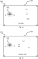
- FIG. 3A shows a first side (top side) of the layout structure 300 of the PCB 306, and Fig. 3B shows a second side (bottom side) of the layout structure 300 of the PCB 306.
- a first footprint 302 is created for the first IC 102.
- the first footprint 302 illustrates locations and dimensions of solder pads and a first thermal pad 308 (can be seen from Fig. 4 ) which will be created on the PCB 306 for the first IC 102.
- Solder pads are the areas on the PCB where the first IC 102's leads or contacts are attached by using solder.
- the first thermal pad 308 may be a copper pad on the PCB where the IC's exposed pad 104 is attached by using solder to dissipate heat generated by the IC 102.
- the thermal pad 308 may be connected to a ground plane through vias to improve heat dissipation.
- a second footprint 310 is created for the second IC 104.
- the second footprint 310 illustrates locations and dimensions of solder pads and a second thermal pad 304 ( Fig. 4 ) which will be created on the PCB 306 for the second IC 106.
- the second thermal pad 304 may be a copper pad on the PCB 306 where the second IC 106's exposed pad 108 is attached by using solder to dissipate heat generated by the second IC 106.
- the first thermal pad 308 and the second thermal pad 304 can be observed from Fig. 4 , which is a cross sectional view of the PCB 306 along line AA'.
- the layout structure 300 may also include footprints for other electronic components or ICs that are illustrated as dashed rectangles. It goes without saying that the layout structure 300 is for illustration purpose only. The number and variety of electronic components or ICs can be selected as needed, and they can be positioned anywhere on the PCB to fulfil actual application needs.
- Fig. 4A is a cross sectional view of the portion of the PCB 306 with thermal pads according to the embodiment.
- the first thermal pad 308 is provided on the first side (top side) of the PCB 306, and the second thermal pad 304 is provided on the second side (bottom side) of the PCB 306.
- the first thermal pad 308 at least partially overlaps with the second thermal pad 304 in a direction perpendicular to the plane of PCB 306.
- a plurality of thermal vias 406 may be provided in the PCB 306 to facilitate heat dissipation.
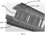
- the first thermal pad 308 and the second thermal pad 304 are connected by the plurality of thermal vias 406, with one end of each thermal via connecting to the first thermal pad 308 and the other end connecting to the second thermal pad 304. This ensures that the openings of the thermal vias 406 at the surface of the PCB are in direct contact with the corresponding thermal pads, establishing a reliable thermal connection.
- the thermal vias 406 can be designed as through-holes traversing the thermal pads and the PCB, with the openings of the vias ends at the outer surfaces of the thermal pads. Such design can simplify the production of the PCB and reduce the production costs subsequently.
- the thermal vias may be designed as such that only a portion of them penetrate the PCB and/or the thermal pads, while the remaining portion may connect to one or more thermal planes within the PCB. In other words, the design of the thermal vias can be modified as needed based on actual needs.
- FIG. 5 A three-dimensional view of the structure of the thermal pads and thermal vias on the PCB, particularly in the area where the thermal pads overlap, can be observed from Fig. 5 .
- the first thermal pad and the second thermal pad fully overlap with each other (have a same dimension).
- the dimensions of the two thermal pads do not have to be identical.
- the first thermal pad 308 may have a dimension of 5mm*5mm
- the second thermal pad 304 may have a dimension of 7mm*7mm.
- heat dissipation of the IC soldered on the smaller thermal pad may be further facilitated by the larger unoccupied thermal pad positioning on the opposite side of the IC.
- centroids geometric center
- the centroids geometric center of the two thermal pads are aligned and overlap in the direction perpendicular to the plane of the PCB, so that heat dissipated by the thermal pads would not affect the function of components on the opposite side of the PCB. Also, such arrangement may provide an efficient way of utilizing the areas on the PCB.
- the first IC 102 is soldered on the top side of the PCB 306 at a specific location that corresponds to the first footprint 302.
- the exposed pad 104 of the first IC 102 is applied (soldered) on the first thermal pad 308 through a first solder 310.
- the second thermal pad 304 remains unoccupied (free from being connected to any component).
- the thermal pad 308 along with the thermal vias 406 dissipates heat generated by the first IC 102.
- the heat dissipation effect is further improved by the existence of the second thermal pad 304.
- the second IC 106 is soldered on the bottom side of the PCB 306 at a specific location that corresponds to the second footprint 310.
- the exposed pad 108 of the second IC 106 is applied (soldered) on the second thermal pad 304 through a second solder 312.
- the first thermal pad remains unoccupied (free from being attached to any component).
- the thermal pad 304 along with the thermal vias 406 dissipates heat generated by the second IC 106.
- the heat dissipation effect is further improved by the existence of the first thermal pad 308. It goes without saying that in the implementations, contact leads of the first IC 102 and the second IC 106 are also soldered on corresponding solder pads of the PCB.
- thermal pads While it is preferable to populate only one of the thermal pads with an IC at a time to optimize heat dissipation, it is conceivable that both thermal pads can be used if the ICs produce minimal heat during operation.
- the ICs 102 and 106 may be a video serializer and a video deserializer having exposed pads with same or different dimensions, respectively.
- the video serializer is implemented, it is mounted on the side of the PCB that is dedicated for the video serializer, and the other side of the PCB is left free.
- the video deserializer is implemented, it is mounted on the side of the PCB that is dedicated for the video deserializer, and the other side of the PCB is left free.
- Other ICs such as radio frequency modulators and demodulators, digital-to-analog converters, analog-to-digital converters, or wireless transmitters and receivers, may be selected based on specific needs. In other words, the ICs that can be populated are not limited to any type.
- both the first thermal pad 308 and the second thermal pad 304 may be unoccupied.
- further thermal pads may be included on the PCB, for example, third and fourth thermal pads, the further thermal pads may be arranged in a similar way as described above.
- the PCB layout according to the present disclosure takes advantage of both the top and bottom sides of the board to include thermal pads for ICs in an overlapping arrangement. This design and the produced PCB make efficient use of space that would otherwise go unused due to the thermal characteristics of an IC having an exposed pad. Specifically, traditionally, the side of the PCB opposite to an IC with an exposed pad is intentionally left unused to enable effective heat dissipation during operation.
- the present disclosure adapts a single PCB for multiple applications involving using different ICs having exposed pads. Consequently, the PCB can be made more compact, and the production and certification cost of PCBs can be significantly reduced.
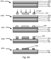
- Fig. 6A and 6B are sectional views sequentially illustrating the process of fabricating a PCB according to an exemplary embodiment.
- a layer of photoresist 608 is applied on a substrate.
- the photoresist may be a positive photoresist or a negative photoresist.
- the substrate may be a copper clad laminate including a laminate 602 sandwiched by two copper layers 604 and 606. In addition to the copper clad laminate shown in Fig. 6 , another laminate with multiple layers of copper pads may also be used.
- the choice of the substrate depends on specific requirements of the PCB, such as desired electrical properties, mechanical strength, and environmental conditions.
- the substrate is exposed to UV light through a photomask 610, which is a mask that has the pattern of the desired electrodes, e.g. the solder pads and the thermal pad of the first IC 102.
- a photomask 610 which is a mask that has the pattern of the desired electrodes, e.g. the solder pads and the thermal pad of the first IC 102.
- the process shown in Fig. 6 uses a positive photoresist.
- the photoresist dissolves away at the areas that were exposed to light, leaving behind a patterned layer on the substrate, as shown in 600c.
- the copper layer 604 is etched to form the pattern shown in step 600d.
- the remained photoresist 608 is dissolved and the first thermal pad 308 is formed. The process is repeated for the other side of the PCB.
- the photoresist 612 is applied on the copper layer 606.
- the substrate is exposed to UV light through a photomask 610, which is a mask that has the pattern of the desired electrodes, e.g. the solder pads and the thermal pad of the second IC 106.
- the photoresist dissolves away at the areas that were exposed to light, leaving behind a patterned layer on the substrate, as shown in 600h.
- the copper layer 606 is etched to form the pattern shown step 600i.
- the remained photoresist 608 is dissolved and the second thermal pad 304 is formed.
- thermal vias is formed in the PCB.
- the formation of thermal vias may be achieved through various methods, including mechanical drilling, laser drilling, or any other suitable method.
- Mechanical drilling involves the use of a drill bit to create holes in the PCB. The size and shape of the holes may vary depending on the design and requirements of the PCB.
- laser drilling may also be used to create the thermal vias.
- This method uses a high-powered laser to remove material from the PCB and create the required holes.
- copper plating may be applied to the inner walls of the vias to enhance thermal conductivity.
- the plating material used may vary, depending on the design specifications of the PCB.
- the PCB produced in this process is similar to that shown in Fig.
- the step 600k may also be performed before forming the thermal pads and the contact pads. That is, before the step 600a.
- the thermal vias 406 (along with other vias) can be drilled before forming the thermal pads and the contact pads.
- a laminate material may be firstly drilled to form the thermal vias.
- a layer of copper may be applied on the laminate by sputtering and electro-chemical deposition.
- lithography process similar as described above may be used to form the thermal pads and contact pads.
- the first thermal pad 308 may be formed in a way in which it at least partially overlaps with the second thermal pad 304 in a direction perpendicular to the plane of PCB 306. It may be possible that the first thermal pad 308 and the second thermal pad 304 may be formed in a way that they fully overlap in the direction perpendicular to the plane of the PCB 306. This may be the case when the first thermal pad 308 and the second thermal pad 306 have a same dimension. It goes without saying that the dimensions of the two thermal pads do not have to be identical.
- centroids (geometric center) of the two thermal pads are aligned and overlap in the direction perpendicular to the plane of the PCB, so that heat dissipated by the thermal pads would not affect the function of components on the opposite side of the PCB.
- further thermal pads may be formed on the PCB by the process as described above or by similar processes.
- a solder mask which is a protective coating applied to the surface of the PCB to protect the copper traces and prevent solder from bridging between adjacent traces.
- the process may include applying a surface finish to protect the exposed copper and improve the electrical conductivity of the traces.
- the process may further include testing and inspection to ensure that the final device meets the required specifications and is free from defects. This may involve a range of tests, such as electrical testing, mechanical testing, and visual inspection.
Landscapes
- Engineering & Computer Science (AREA)
- Microelectronics & Electronic Packaging (AREA)
- Manufacturing & Machinery (AREA)
- Physics & Mathematics (AREA)
- Electromagnetism (AREA)
- Structure Of Printed Boards (AREA)
Priority Applications (3)
| Application Number | Priority Date | Filing Date | Title |
|---|---|---|---|
| EP23169228.6A EP4451812A1 (fr) | 2023-04-21 | 2023-04-21 | Carte de circuit imprimé et son procédé de production |
| US18/635,534 US20240357730A1 (en) | 2023-04-21 | 2024-04-15 | Printed circuit board and method of producing thereof |
| CN202410476838.1A CN118829075A (zh) | 2023-04-21 | 2024-04-19 | 印刷电路板及其生产方法 |
Applications Claiming Priority (1)
| Application Number | Priority Date | Filing Date | Title |
|---|---|---|---|
| EP23169228.6A EP4451812A1 (fr) | 2023-04-21 | 2023-04-21 | Carte de circuit imprimé et son procédé de production |
Publications (1)
| Publication Number | Publication Date |
|---|---|
| EP4451812A1 true EP4451812A1 (fr) | 2024-10-23 |
Family
ID=86142833
Family Applications (1)
| Application Number | Title | Priority Date | Filing Date |
|---|---|---|---|
| EP23169228.6A Pending EP4451812A1 (fr) | 2023-04-21 | 2023-04-21 | Carte de circuit imprimé et son procédé de production |
Country Status (3)
| Country | Link |
|---|---|
| US (1) | US20240357730A1 (fr) |
| EP (1) | EP4451812A1 (fr) |
| CN (1) | CN118829075A (fr) |
Families Citing this family (1)
| Publication number | Priority date | Publication date | Assignee | Title |
|---|---|---|---|---|
| US12380311B2 (en) * | 2023-03-22 | 2025-08-05 | Smartflex Technology Pte Ltd | Articles of manufacture relating to IC modules and smart cards |
Citations (4)
| Publication number | Priority date | Publication date | Assignee | Title |
|---|---|---|---|---|
| US5982630A (en) * | 1997-11-06 | 1999-11-09 | Intel Corporation | Printed circuit board that provides improved thermal dissipation |
| DE102005063281A1 (de) * | 2005-12-30 | 2007-07-05 | Robert Bosch Gmbh | Integriertes elektronisches Bauteil sowie Kühlvorrichtung für ein integriertes elektronisches Bauteil |
| US7707715B2 (en) | 2007-08-31 | 2010-05-04 | Samsung Electro-Mechanics, Co., Ltd. | Method of fabricating multilayer printed circuit board |
| EP3110238A2 (fr) * | 2015-06-26 | 2016-12-28 | Delta Electronics, Inc. | Structure d'ensemble et dispositif électronique muni de celle-ci |
Family Cites Families (9)
| Publication number | Priority date | Publication date | Assignee | Title |
|---|---|---|---|---|
| US5741729A (en) * | 1994-07-11 | 1998-04-21 | Sun Microsystems, Inc. | Ball grid array package for an integrated circuit |
| US5769989A (en) * | 1995-09-19 | 1998-06-23 | International Business Machines Corporation | Method and system for reworkable direct chip attach (DCA) structure with thermal enhancement |
| US6212076B1 (en) * | 1999-02-26 | 2001-04-03 | International Business Machines Corporation | Enhanced heat-dissipating printed circuit board package |
| US6867493B2 (en) * | 2000-11-15 | 2005-03-15 | Skyworks Solutions, Inc. | Structure and method for fabrication of a leadless multi-die carrier |
| WO2003065719A1 (fr) * | 2002-01-30 | 2003-08-07 | Gennum Corporation | Convertisseur parallele-serie / convertisseur serie-parallele video a support audio integre |
| US7148554B2 (en) * | 2004-12-16 | 2006-12-12 | Delphi Technologies, Inc. | Discrete electronic component arrangement including anchoring, thermally conductive pad |
| US7606034B2 (en) * | 2006-06-05 | 2009-10-20 | Corsair Memory | Thermally enhanced memory module |
| EP3240372A1 (fr) * | 2016-04-27 | 2017-11-01 | AT & S Austria Technologie & Systemtechnik Aktiengesellschaft | Support de composant capacitif de chaleur et procédé pour produire ce composant support |
| JP2025022428A (ja) * | 2023-08-03 | 2025-02-14 | キヤノン株式会社 | 回路基板、画像形成装置 |
-
2023
- 2023-04-21 EP EP23169228.6A patent/EP4451812A1/fr active Pending
-
2024
- 2024-04-15 US US18/635,534 patent/US20240357730A1/en active Pending
- 2024-04-19 CN CN202410476838.1A patent/CN118829075A/zh active Pending
Patent Citations (4)
| Publication number | Priority date | Publication date | Assignee | Title |
|---|---|---|---|---|
| US5982630A (en) * | 1997-11-06 | 1999-11-09 | Intel Corporation | Printed circuit board that provides improved thermal dissipation |
| DE102005063281A1 (de) * | 2005-12-30 | 2007-07-05 | Robert Bosch Gmbh | Integriertes elektronisches Bauteil sowie Kühlvorrichtung für ein integriertes elektronisches Bauteil |
| US7707715B2 (en) | 2007-08-31 | 2010-05-04 | Samsung Electro-Mechanics, Co., Ltd. | Method of fabricating multilayer printed circuit board |
| EP3110238A2 (fr) * | 2015-06-26 | 2016-12-28 | Delta Electronics, Inc. | Structure d'ensemble et dispositif électronique muni de celle-ci |
Also Published As
| Publication number | Publication date |
|---|---|
| US20240357730A1 (en) | 2024-10-24 |
| CN118829075A (zh) | 2024-10-22 |
Similar Documents
| Publication | Publication Date | Title |
|---|---|---|
| JP6682741B2 (ja) | 回路基板及び回路基板組立体 | |
| US7751202B2 (en) | Multi-layered printed circuit board having integrated circuit embedded therein | |
| TWI513379B (zh) | 內埋元件的基板結構與其製造方法 | |
| US7985926B2 (en) | Printed circuit board and electronic component device | |
| US8134841B2 (en) | Printed-wiring board, method of manufacturing printed-wiring board, and electronic equipment | |
| CN101309559B (zh) | 多层印刷电路板及其设计方法和终端产品主板 | |
| KR20150060101A (ko) | 볼 랜드를 포함하는 기판 및 반도체 패키지와, 그 제조방법 | |
| KR20150064976A (ko) | 인쇄회로기판 및 그 제조방법 | |
| EP4451812A1 (fr) | Carte de circuit imprimé et son procédé de production | |
| JP2005236067A (ja) | 配線基板と配線基板の製造方法、および半導パッケージ | |
| KR20150065029A (ko) | 인쇄회로기판, 그 제조방법 및 반도체 패키지 | |
| US9076801B2 (en) | Module IC package structure | |
| US20110019379A1 (en) | Printed wiring board, semiconductor device, and method for manufacturing printed wiring board | |
| JP4498479B2 (ja) | マルチボンド棚プラスチックパッケージの製造方法 | |
| US11903146B2 (en) | Printed wiring board and method for manufacturing printed wiring board | |
| KR100916697B1 (ko) | 수동소자가 직접 내장된 인쇄회로기판의 제작방법 | |
| TWI763530B (zh) | 探針卡測試裝置 | |
| KR101796519B1 (ko) | 회로기판 및 회로기판 조립체 | |
| KR20150136914A (ko) | 인쇄회로기판의 제조방법 | |
| KR20150009671A (ko) | 금속 포스트를 구비한 인쇄회로기판 및 이의 제조 방법 | |
| US20080123273A1 (en) | Circuit Board Including Stubless Signal Paths and Method of Making Same | |
| US20040182603A1 (en) | [inner layer structure of a circuit board] | |
| KR100693145B1 (ko) | 인쇄회로기판의 제조방법 | |
| JP2016134476A (ja) | プリント配線板及びプリント配線板の製造方法 | |
| KR102770661B1 (ko) | 양면 구리의 연성 회로 기판 |
Legal Events
| Date | Code | Title | Description |
|---|---|---|---|
| PUAI | Public reference made under article 153(3) epc to a published international application that has entered the european phase |
Free format text: ORIGINAL CODE: 0009012 |
|
| STAA | Information on the status of an ep patent application or granted ep patent |
Free format text: STATUS: THE APPLICATION HAS BEEN PUBLISHED |
|
| AK | Designated contracting states |
Kind code of ref document: A1 Designated state(s): AL AT BE BG CH CY CZ DE DK EE ES FI FR GB GR HR HU IE IS IT LI LT LU LV MC ME MK MT NL NO PL PT RO RS SE SI SK SM TR |
|
| STAA | Information on the status of an ep patent application or granted ep patent |
Free format text: STATUS: REQUEST FOR EXAMINATION WAS MADE |
|
| 17P | Request for examination filed |
Effective date: 20250423 |