EP3131116A1 - Herstellungsverfahren einer elektronischen vorrichtung - Google Patents
Herstellungsverfahren einer elektronischen vorrichtung Download PDFInfo
- Publication number
- EP3131116A1 EP3131116A1 EP16181484.3A EP16181484A EP3131116A1 EP 3131116 A1 EP3131116 A1 EP 3131116A1 EP 16181484 A EP16181484 A EP 16181484A EP 3131116 A1 EP3131116 A1 EP 3131116A1
- Authority
- EP
- European Patent Office
- Prior art keywords
- substrate
- face
- support
- substrates
- mark
- Prior art date
- Legal status (The legal status is an assumption and is not a legal conclusion. Google has not performed a legal analysis and makes no representation as to the accuracy of the status listed.)
- Withdrawn
Links
Images

Classifications
-
- H—ELECTRICITY
- H05—ELECTRIC TECHNIQUES NOT OTHERWISE PROVIDED FOR
- H05K—PRINTED CIRCUITS; CASINGS OR CONSTRUCTIONAL DETAILS OF ELECTRIC APPARATUS; MANUFACTURE OF ASSEMBLAGES OF ELECTRICAL COMPONENTS
- H05K3/00—Apparatus or processes for manufacturing printed circuits
- H05K3/0011—Working of insulating substrates or insulating layers
- H05K3/0017—Etching of the substrate by chemical or physical means
-
- H—ELECTRICITY
- H05—ELECTRIC TECHNIQUES NOT OTHERWISE PROVIDED FOR
- H05K—PRINTED CIRCUITS; CASINGS OR CONSTRUCTIONAL DETAILS OF ELECTRIC APPARATUS; MANUFACTURE OF ASSEMBLAGES OF ELECTRICAL COMPONENTS
- H05K3/00—Apparatus or processes for manufacturing printed circuits
- H05K3/30—Assembling printed circuits with electric components, e.g. with resistors
-
- H—ELECTRICITY
- H10—SEMICONDUCTOR DEVICES; ELECTRIC SOLID-STATE DEVICES NOT OTHERWISE PROVIDED FOR
- H10D—INORGANIC ELECTRIC SEMICONDUCTOR DEVICES
- H10D84/00—Integrated devices formed in or on semiconductor substrates that comprise only semiconducting layers, e.g. on Si wafers or on GaAs-on-Si wafers
-
- H—ELECTRICITY
- H10—SEMICONDUCTOR DEVICES; ELECTRIC SOLID-STATE DEVICES NOT OTHERWISE PROVIDED FOR
- H10P—GENERIC PROCESSES OR APPARATUS FOR THE MANUFACTURE OR TREATMENT OF DEVICES COVERED BY CLASS H10
- H10P10/00—Bonding of wafers, substrates or parts of devices
- H10P10/12—Bonding of semiconductor wafers or semiconductor substrates to semiconductor wafers or semiconductor substrates
- H10P10/128—Bonding of semiconductor wafers or semiconductor substrates to semiconductor wafers or semiconductor substrates by direct semiconductor to semiconductor bonding
-
- H—ELECTRICITY
- H10—SEMICONDUCTOR DEVICES; ELECTRIC SOLID-STATE DEVICES NOT OTHERWISE PROVIDED FOR
- H10P—GENERIC PROCESSES OR APPARATUS FOR THE MANUFACTURE OR TREATMENT OF DEVICES COVERED BY CLASS H10
- H10P90/00—Preparation of wafers not covered by a single main group of this subclass, e.g. wafer reinforcement
- H10P90/19—Preparing inhomogeneous wafers
- H10P90/1904—Preparing vertically inhomogeneous wafers
- H10P90/1906—Preparing SOI wafers
- H10P90/1914—Preparing SOI wafers using bonding
- H10P90/1916—Preparing SOI wafers using bonding with separation or delamination along an ion implanted layer, e.g. Smart-cut
-
- H—ELECTRICITY
- H10—SEMICONDUCTOR DEVICES; ELECTRIC SOLID-STATE DEVICES NOT OTHERWISE PROVIDED FOR
- H10W—GENERIC PACKAGES, INTERCONNECTIONS, CONNECTORS OR OTHER CONSTRUCTIONAL DETAILS OF DEVICES COVERED BY CLASS H10
- H10W10/00—Isolation regions in semiconductor bodies between components of integrated devices
- H10W10/10—Isolation regions comprising dielectric materials
- H10W10/181—Semiconductor-on-insulator [SOI] isolation regions, e.g. buried oxide regions of SOI wafers
-
- H—ELECTRICITY
- H10—SEMICONDUCTOR DEVICES; ELECTRIC SOLID-STATE DEVICES NOT OTHERWISE PROVIDED FOR
- H10W—GENERIC PACKAGES, INTERCONNECTIONS, CONNECTORS OR OTHER CONSTRUCTIONAL DETAILS OF DEVICES COVERED BY CLASS H10
- H10W46/00—Marks applied to devices, e.g. for alignment or identification
-
- H—ELECTRICITY
- H10—SEMICONDUCTOR DEVICES; ELECTRIC SOLID-STATE DEVICES NOT OTHERWISE PROVIDED FOR
- H10W—GENERIC PACKAGES, INTERCONNECTIONS, CONNECTORS OR OTHER CONSTRUCTIONAL DETAILS OF DEVICES COVERED BY CLASS H10
- H10W90/00—Package configurations
-
- H—ELECTRICITY
- H10—SEMICONDUCTOR DEVICES; ELECTRIC SOLID-STATE DEVICES NOT OTHERWISE PROVIDED FOR
- H10D—INORGANIC ELECTRIC SEMICONDUCTOR DEVICES
- H10D84/00—Integrated devices formed in or on semiconductor substrates that comprise only semiconducting layers, e.g. on Si wafers or on GaAs-on-Si wafers
- H10D84/01—Manufacture or treatment
- H10D84/02—Manufacture or treatment characterised by using material-based technologies
- H10D84/03—Manufacture or treatment characterised by using material-based technologies using Group IV technology, e.g. silicon technology or silicon-carbide [SiC] technology
- H10D84/038—Manufacture or treatment characterised by using material-based technologies using Group IV technology, e.g. silicon technology or silicon-carbide [SiC] technology using silicon technology, e.g. SiGe
-
- H—ELECTRICITY
- H10—SEMICONDUCTOR DEVICES; ELECTRIC SOLID-STATE DEVICES NOT OTHERWISE PROVIDED FOR
- H10D—INORGANIC ELECTRIC SEMICONDUCTOR DEVICES
- H10D88/00—Three-dimensional [3D] integrated devices
- H10D88/01—Manufacture or treatment
-
- H—ELECTRICITY
- H10—SEMICONDUCTOR DEVICES; ELECTRIC SOLID-STATE DEVICES NOT OTHERWISE PROVIDED FOR
- H10W—GENERIC PACKAGES, INTERCONNECTIONS, CONNECTORS OR OTHER CONSTRUCTIONAL DETAILS OF DEVICES COVERED BY CLASS H10
- H10W46/00—Marks applied to devices, e.g. for alignment or identification
- H10W46/301—Marks applied to devices, e.g. for alignment or identification for alignment
-
- H—ELECTRICITY
- H10—SEMICONDUCTOR DEVICES; ELECTRIC SOLID-STATE DEVICES NOT OTHERWISE PROVIDED FOR
- H10W—GENERIC PACKAGES, INTERCONNECTIONS, CONNECTORS OR OTHER CONSTRUCTIONAL DETAILS OF DEVICES COVERED BY CLASS H10
- H10W46/00—Marks applied to devices, e.g. for alignment or identification
- H10W46/501—Marks applied to devices, e.g. for alignment or identification for use before dicing
-
- H—ELECTRICITY
- H10—SEMICONDUCTOR DEVICES; ELECTRIC SOLID-STATE DEVICES NOT OTHERWISE PROVIDED FOR
- H10W—GENERIC PACKAGES, INTERCONNECTIONS, CONNECTORS OR OTHER CONSTRUCTIONAL DETAILS OF DEVICES COVERED BY CLASS H10
- H10W72/00—Interconnections or connectors in packages
- H10W72/90—Bond pads, in general
- H10W72/941—Dispositions of bond pads
-
- H—ELECTRICITY
- H10—SEMICONDUCTOR DEVICES; ELECTRIC SOLID-STATE DEVICES NOT OTHERWISE PROVIDED FOR
- H10W—GENERIC PACKAGES, INTERCONNECTIONS, CONNECTORS OR OTHER CONSTRUCTIONAL DETAILS OF DEVICES COVERED BY CLASS H10
- H10W80/00—Direct bonding of chips, wafers or substrates
- H10W80/211—Direct bonding of chips, wafers or substrates using auxiliary members, e.g. aids for protecting the bonding area
-
- H—ELECTRICITY
- H10—SEMICONDUCTOR DEVICES; ELECTRIC SOLID-STATE DEVICES NOT OTHERWISE PROVIDED FOR
- H10W—GENERIC PACKAGES, INTERCONNECTIONS, CONNECTORS OR OTHER CONSTRUCTIONAL DETAILS OF DEVICES COVERED BY CLASS H10
- H10W80/00—Direct bonding of chips, wafers or substrates
- H10W80/301—Bonding techniques, e.g. hybrid bonding
-
- H—ELECTRICITY
- H10—SEMICONDUCTOR DEVICES; ELECTRIC SOLID-STATE DEVICES NOT OTHERWISE PROVIDED FOR
- H10W—GENERIC PACKAGES, INTERCONNECTIONS, CONNECTORS OR OTHER CONSTRUCTIONAL DETAILS OF DEVICES COVERED BY CLASS H10
- H10W90/00—Package configurations
- H10W90/701—Package configurations characterised by the relative positions of pads or connectors relative to package parts
- H10W90/791—Package configurations characterised by the relative positions of pads or connectors relative to package parts of direct-bonded pads
- H10W90/792—Package configurations characterised by the relative positions of pads or connectors relative to package parts of direct-bonded pads between multiple chips
Definitions
- the invention relates to a method for producing an electronic device comprising in stacking at least a first structure and a second structure.
- An interest of the invention is to allow proper alignment of the stacked structures. It finds particular application in the manufacture of three-dimensional microelectronic devices, for which the components are no longer or only located in a single plane of a substrate, but are also produced in superposition, thanks to superposed layers of substrates incorporating components. . More specifically, the present invention applies for example to the production of backlit imagers and to the production of the stack of two CMOS substrates.
- Three-dimensional devices require structural assemblies (typically substrates that have undergone processing).
- the proper matching of these structures is a fundamental issue for the reliability of the final device and to reduce the size of the components, such as electrical contacts on the surface of two structures and they should cooperate.
- a first misalignment is due to the accuracy of alignment of the transfer of a substrate on the other. This misalignment, global because it concerns all the patterns, is found in particular by measuring the misalignment between the primary marks of the first substrate vis-à-vis the primary marks of the second substrate.
- a second misalignment is that of the secondary alignment marks vis-à-vis the primary marks within the same substrate during their production.
- This misalignment is in fact a bad positioning of the secondary marks in relation to the primary marks. It can be of the order of plus or minus 50nm for example. But this misplacement will imply a poor overall positioning of unit area patterns relative to the primary alignment marks. This defect can occur even if the first source of misalignment, mentioned in the previous paragraph, is weak or non-existent.
- the patterns of the first substrate will not be properly aligned with the patterns of the second substrate. As this misalignment can occur randomly and has a random amplitude for each unit area, it is very difficult, if not impossible, to correct it during the global alignment of the substrates for the report.
- a third source of misalignment is due to plate deformation of the substrates during the carryover operation.
- direct bonding causes distortions. These distortions can modify the relative placement of the secondary marks because they are precisely located at the bonding interface.
- These displacements of the alignment marks may be large enough to prevent the realization of subsequent technological processes.
- the distortion can prevent lithography machines to find secondary alignment marks thus preventing other lithography steps.
- the present invention overcomes all or part of the technical disadvantages currently known.
- Another aspect of embodiments of the invention is directed to a device that can be obtained by the method of the invention.
- the marks of the first structure and of the second structure find their origin in a single brand pattern so that they are perfectly coherent.
- the method follows a pattern of continuity of placement of the structures in supports that are identical for both the assembly operation of the starting substrates and for the assembly operation of the final structures. This removes the risk of misalignment between the first mark and the second mark so that the stacking of the two structures is very accurate in its location.
- the method of the invention makes it possible to manufacture a so-called electronic device in that it comprises electrical parts on structures which may, preferably, comprise a substrate for example made of semiconductor material, in particular silicon-based material.
- substrate means any semiconductor medium or not, forming all or part of a structure. It can be mono or multilayer.
- the orientation of the substrate defines, on both sides of its thickness, two faces.
- one of the faces of a given substrate can cooperate with a support, which is preferably an element of a tool used during manufacture.
- the other side can be used to carry out treatments such as formation of layers above the substrate, formation of patterns in the substrate and / or added layers, formation of simple electronic components (such as electrical distribution lines) or complex (such as transistors).
- electronic component refers to any organ that may have application in the field of electronics and microelectronics.
- electronic component is not limited to components having an electrical function. It is not excluded that the first side also be used for treatments, for example in a phase subsequent to those presented here. Treatments may also include formation of components passing through the thickness of the substrate, such as vias.
- the device manufactured according to the invention is derived from a stack of structures based on substrates as mentioned in the previous paragraph. It can be a microelectronic device. By microelectronics is meant in particular all the techniques of microelectronics and nanoelectronics.
- the devices that can be formed can be part of systems of the micro-electro-mechanical systems called MEMS and / or with optical functions.
- thickness means, unless otherwise provided, a dimension according to the thickness of the substrate or substrates, for example perpendicular to a plane of a surface of the substrate.
- width means, unless otherwise provided, a dimension perpendicular to the thickness of the substrate.
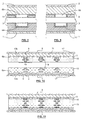
- the figure 1 shows an example of configuration of two structures to assemble.
- a first structure 15 is here in the lower position and has a base issuing from a first substrate 3 described later surmounted by a functional assembly 13, for example in the form of a plurality of layers and / or components 18 fulfilling a function especially electric. These components are simply schematized by patterns of materials different from the rest of the layer or layers that contain them.
- the first substrate 3 may equally well include components. For example vias (such as TSV, English Through Silicon Via) can be formed. The invention therefore makes no assumptions about the configuration of the first structure 15.
- figure 1 shows a second structure 16. It comprises a base of which a first face 11 is derived from a second substrate 9, and a functional assembly 14. The indications given previously for this type of structural component 18, with reference to the first structure 15 are valid for the second structure 16.
- the second structure 16 is oriented so that a face to be assembled is facing a face to associate him with the first structure 15, these faces being advantageously directed in planes parallel and perpendicular to the thickness of the substrates.
- brands not illustrated in figure 1
- An alignment is understood to mean the matching of the two structures in a plane perpendicular to their thickness. This makes it possible, in particular, to bring electrical members exposed to the surface of the two structures 15, 16 into contact with each other.
- Other marks (not illustrated in FIG. figure 1 ), said secondary, can also be used in areas 19 embodiment of electronic chips.
- the invention can serve, on the basis of plates, for example from silicon, to produce in a group, a plurality of chips of the same type, chips which are distributed on the surface of the plates and which will then be individualized by zones cutting.
- Chip means any electronic system whose components mentioned above.
- the secondary marks can be reproduced in each zone 19 to serve as proximity marks to the machines used to manufacture the chips.
- a starting step can start from a first substrate 3, for example silicon, which can typically be a circular plate (or wafer in English) of 300 mm in diameter; its resistivity is in an example of 14 ohm / cm with a P-type doping.
- a first substrate 3 for example silicon, which can typically be a circular plate (or wafer in English) of 300 mm in diameter; its resistivity is in an example of 14 ohm / cm with a P-type doping.
- the weakened zone 8 is understood to mean a zone located in the thickness of the substrate 3 and preferably not exposed to the surface of the substrate 3, having a lower mechanical strength than the surrounding areas.
- This embrittlement can be obtained by an ion implantation of hydrogen atoms with an energy of 55keV with a dose of 6.10 16 at / cm 2 to place the level of the hydrogen implantation peak at 150 nm from the bottom of the pattern 6 alignment marks.
- the implantation peak is thus advantageously in the thickness of the pattern 6 which is formed either before or afterwards. figure 4 .
- the weakened zone 8 may consist of a layer of the substrate 3, with different mechanical properties of the other layers.
- the manufacture of the substrate 3 may comprise the formation of a porous layer followed by growth of a non-porous layer, so that the porous layer internal to the substrate is the site of a weakening of the latter.
- the pattern 6 is made on the second face 4 of the substrate 3 which will serve to create two marks 6a, 6b each on one of the structures 15, 16, this common origin of the marks ensuring their perfect alignment.
- the pattern can be engraved with, for example, photolithography steps.
- the depth (marked "a” in figure 4 ) of etching, in the first substrate 3 made of silicon, for example, these marks is optionally 350 nm.
- a rectangular or square section pattern may be suitable but other shapes are possible.
- an electrically insulating layer 7 having a thickness "b" is produced, preferably by thermal oxidation which can be carried out at 950 ° C. under steam to obtain an oxide layer of 100 nm thickness which consumes a little substrate 3 from its second side 4, about 50nm in the case of silicon. The result is visible in figure 5 .
- This layer 7 can serve, alternatively or cumulatively to the insulation function, serve to facilitate direct bonding.
- a second substrate 9 is then used. It can also be made of silicon, for example 300mm in diameter whose resistivity is 14ohm / cm with P type doping.
- the two substrates 3, 9 can be of different formats.
- the two substrates then undergo optional cleaning, typically chemical with a first cleaning using a known solution of sulfuric acid, hydrogen peroxide in the proportions 3: 1, using a solution of sulfuric acid at 96% by volume and a solution of d hydrogen peroxide at 30% by volume.
- the cleaning time is for example 10 minutes to 180 ° C.
- a second cleaning is carried out, not limited to ammonia, hydrogen peroxide and deionized water in the proportions 1: 1: 5 using ammonia and water. hydrogen peroxide at 30% by volume for 10 minutes at 71 ° C.
- the substrates 3, 9 are then rinsed and dried.
- the first substrate 3 is then placed on a support 1 by its first face 5 for securing it in position during processing steps.
- the support 1 is in particular a chuck generally called "chuck" in English.
- the support 1 comprises in the example a tray with a surface, advantageously flat, capable of receiving a first face 5 of the substrate 3. It may comprise elements for holding the substrate 3, in particular by suction on a ring 17 visible in figure 10 opening at the first face 5 and connected to a vacuum circuit. But other means of attachment can exist.
- the second substrate 9 is also carried by a support 2 with which it cooperates with its first face 11. It is possible to use a support 2 of the same technology as the first support 1.
- the substrates 3, 9 are brought closer to each other at a distance of, for example, 70 ⁇ m, as in figure 6 .
- Local deformation in the center of the second substrate 9 can initiate contacting.
- This contacting step can last 20 seconds after the support force is reached (such as 3500 mN).
- the vacuum of the top plate is removed, allowing the bonding to end by releasing the second substrate 9 of the second support 2.
- the vacuum of first substrate 3 is released and the bonding is completed.
- the configuration of the figure 7 is reached.
- the adhesion energy used for this first direct bonding is preferably 110 mJ / m 2 .
- the arrow of each substrate 3, 9 before bonding is for example 10 microns.
- the bonding occurs at a temperature below 100 ° C, preferably above 5 ° C and in particular ambient, for example 21 ° C.
- a separation into two parts of the previously obtained assembly is carried out.
- a thermal annealing (in particular at 500 ° C. for two hours) makes it possible to cause separation at the level of the weakened zone 8 (the peak of hydrogen implantation in figure 7 ).
- Part of the first substrate 3 is then offset with the second substrate 9.
- one option is to polish the surface of the two parts obtained by cleavage of the assembly, for example with mechanical or mechano-chemical polishing.
- the exposed surfaces of the two separate parts are thus more favorable to subsequent treatments, such as figure 9 .
- each substrate may include photolithographic steps, ion etching, thin film deposition and chemical mechanical polishing for example.
- at least one electronic component 18 is formed on each part, these components 18 being able to vary widely according to the applications.
- each structure 15, 16 is preferably performed under the same conditions as during the steps of maintaining the substrates for the first assembly. This step is presented in figure 10 where primary marks 6a, 6b, near each edge of the starting substrates, are visible. They can be organized according to a diameter of the first and second substrates. Also, secondary marks 12a, 12b are formed for each chip formation zone.
- All or part, but advantageously all the conditions of the first direct bonding are taken again for the bonding of the two structures 15, 16.
- the conditions of temperature, atmosphere, preparation of the docking, and direct bonding are preferably all reproduced.
- a maximum tolerance of 1% can for example be taken with regard to the distance identity of the surfaces to be bonded before contacting. It can be at most 10% for the bonding force or 1% for the release times of the faces applied to the supports 1, 2, or +/- 0.1 ° C for the temperature.
- the adhesion energy may possibly vary by up to 20%.
- the arrows should not be modified by more than +/- 10 ⁇ m for a 300 mm diameter and +/- 7 ⁇ m starting plate for a 200 mm diameter starting plate.
- This possible tolerance is preferably the following for the ambient atmosphere of the two collages: pressure at + -1%, type of gas at + -1% in composition, temperature + -0.1 ° C, humidity + -5% deviation between the two relative humidity values of the two collages.
- pressure at + -1% the ambient atmosphere of the two collages
- type of gas at + -1% in composition the ambient atmosphere of the two collages
- temperature + -0.1 ° C the temperature + -0.1 ° C
- humidity + -5% deviation between the two relative humidity values of the two collages For the overall alignment of the two structures during the second bonding will preferably remain below + -5 .mu.m, and more specifically below + -1 .mu.m or 500 nm, or 300 nm or 100 nm.
- the alignment of the structures 15, 16 with respect to the supports 1, 2 is at the beginning and during the second bonding preferably less than + -50 ⁇ m in both directions of the plane of the bonding interface.
- the primary marks 6a, 6b can be used as alignment marks.
- Optical techniques can be used, for example in the infra-red, by transmission through the structures, particularly if they are based on non-heavily doped silicon, allowing a certain transparency. Other techniques such as with microscopes between the structures are usable.
Landscapes
- Engineering & Computer Science (AREA)
- Manufacturing & Machinery (AREA)
- Microelectronics & Electronic Packaging (AREA)
- Micromachines (AREA)
- Pressure Welding/Diffusion-Bonding (AREA)
Applications Claiming Priority (1)
| Application Number | Priority Date | Filing Date | Title |
|---|---|---|---|
| FR1557436A FR3039699B1 (fr) | 2015-07-31 | 2015-07-31 | Procede de realisation d'un dispositif electronique |
Publications (1)
| Publication Number | Publication Date |
|---|---|
| EP3131116A1 true EP3131116A1 (de) | 2017-02-15 |
Family
ID=55022533
Family Applications (1)
| Application Number | Title | Priority Date | Filing Date |
|---|---|---|---|
| EP16181484.3A Withdrawn EP3131116A1 (de) | 2015-07-31 | 2016-07-27 | Herstellungsverfahren einer elektronischen vorrichtung |
Country Status (3)
| Country | Link |
|---|---|
| US (1) | US9769931B2 (de) |
| EP (1) | EP3131116A1 (de) |
| FR (1) | FR3039699B1 (de) |
Families Citing this family (5)
| Publication number | Priority date | Publication date | Assignee | Title |
|---|---|---|---|---|
| US20180175008A1 (en) * | 2015-01-09 | 2018-06-21 | Silicon Genesis Corporation | Three dimensional integrated circuit |
| US10847369B2 (en) * | 2018-12-26 | 2020-11-24 | Samsung Electronics Co., Ltd. | Wafer bonding method, method for manufacturing semiconductor device, and apparatus therefor |
| CN111933618B (zh) * | 2020-08-13 | 2022-01-28 | 武汉新芯集成电路制造有限公司 | 具有对准标识的晶圆组件及其形成方法、晶圆对准方法 |
| KR20230053148A (ko) * | 2021-10-14 | 2023-04-21 | 삼성전자주식회사 | 반도체 칩 및 반도체 패키지 |
| CN118234155B (zh) * | 2024-02-01 | 2025-12-19 | 东莞市锐翔技术有限公司 | 电路板熔合方法及熔合生产线 |
Citations (4)
| Publication number | Priority date | Publication date | Assignee | Title |
|---|---|---|---|---|
| WO2002054466A1 (fr) | 2000-12-28 | 2002-07-11 | Commissariat A L'energie Atomique | Procede de realisation d'une structure empilee |
| US6423614B1 (en) * | 1998-06-30 | 2002-07-23 | Intel Corporation | Method of delaminating a thin film using non-thermal techniques |
| US20120006463A1 (en) * | 2010-07-07 | 2012-01-12 | Gweltaz Gaudin | Method for molecular adhesion bonding with compensation for radial misalignment |
| FR2973569A1 (fr) * | 2011-04-01 | 2012-10-05 | St Microelectronics Sa | Procédé de fabrication d'un circuit intégré comportant au moins un composant haute fréquence et circuit intégré correspondant |
Family Cites Families (5)
| Publication number | Priority date | Publication date | Assignee | Title |
|---|---|---|---|---|
| FR2848725B1 (fr) | 2002-12-17 | 2005-02-11 | Commissariat Energie Atomique | Procede de formation de motifs alignes de part et d'autre d'un film mince |
| EP1482548B1 (de) * | 2003-05-26 | 2016-04-13 | Soitec | Verfahren zur Herstellung von Halbleiterscheiben |
| FR2876220B1 (fr) * | 2004-10-06 | 2007-09-28 | Commissariat Energie Atomique | Procede d'elaboration de structures empilees mixtes, a zones isolantes diverses et/ou zones de conduction electrique verticale localisees. |
| US20070007237A1 (en) * | 2005-07-05 | 2007-01-11 | National Taiwan University | Method for self-assembling microstructures |
| FR2938117B1 (fr) * | 2008-10-31 | 2011-04-15 | Commissariat Energie Atomique | Procede d'elaboration d'un substrat hybride ayant une couche continue electriquement isolante enterree |
-
2015
- 2015-07-31 FR FR1557436A patent/FR3039699B1/fr not_active Expired - Fee Related
-
2016
- 2016-07-27 EP EP16181484.3A patent/EP3131116A1/de not_active Withdrawn
- 2016-07-29 US US15/223,718 patent/US9769931B2/en not_active Expired - Fee Related
Patent Citations (4)
| Publication number | Priority date | Publication date | Assignee | Title |
|---|---|---|---|---|
| US6423614B1 (en) * | 1998-06-30 | 2002-07-23 | Intel Corporation | Method of delaminating a thin film using non-thermal techniques |
| WO2002054466A1 (fr) | 2000-12-28 | 2002-07-11 | Commissariat A L'energie Atomique | Procede de realisation d'une structure empilee |
| US20120006463A1 (en) * | 2010-07-07 | 2012-01-12 | Gweltaz Gaudin | Method for molecular adhesion bonding with compensation for radial misalignment |
| FR2973569A1 (fr) * | 2011-04-01 | 2012-10-05 | St Microelectronics Sa | Procédé de fabrication d'un circuit intégré comportant au moins un composant haute fréquence et circuit intégré correspondant |
Also Published As
| Publication number | Publication date |
|---|---|
| US20170034919A1 (en) | 2017-02-02 |
| FR3039699B1 (fr) | 2017-07-28 |
| FR3039699A1 (fr) | 2017-02-03 |
| US9769931B2 (en) | 2017-09-19 |
Similar Documents
| Publication | Publication Date | Title |
|---|---|---|
| EP1576658B1 (de) | Herstellungsverfahren für gemischte substrate und dadurch hergestellte struktur | |
| EP3131116A1 (de) | Herstellungsverfahren einer elektronischen vorrichtung | |
| EP3593376B1 (de) | Verfahren zur selbstassemblierung von mikroelektronischen bauteilen | |
| FR2935536A1 (fr) | Procede de detourage progressif | |
| FR2819099A1 (fr) | Procede de realisation d'une structure empilee | |
| EP2054929A2 (de) | Prozess zur kollektiven herstellung von elektronischen 3d-modulen | |
| WO2021099713A1 (fr) | Procede de fabrication d'une puce fonctionnelle adaptee pour etre assemblee a des elements filaires | |
| FR2895419A1 (fr) | Procede de realisation simplifiee d'une structure epitaxiee | |
| EP3329511B1 (de) | Verfahren zum direkten bonden mit selbstausrichtung unter verwendung von ultraschall | |
| FR2969378A1 (fr) | Structure composite tridimensionnelle comportant plusieurs couches de microcomposants en alignement | |
| EP4085478B1 (de) | Verfahren zur herstellung einer verbundstruktur mit einer dünnen monokristallinen schicht auf einem trägersubstrat | |
| EP3497711B1 (de) | Verfahren zur herstellung einer epitaktischen schicht auf einem züchtungssubstrat | |
| BE1023710B1 (fr) | Procede de separation mecanique pour un double transfert de couche | |
| EP3552226B1 (de) | Verfahren zur übertragung von dünnschichten | |
| EP2676288A1 (de) | Verfahren zur herstellung einer substrathalterung | |
| FR2895391A1 (fr) | Procede d'elaboration de nanostructures ordonnees | |
| WO2016156279A1 (fr) | Procédé d'assemblage de substrats | |
| EP3776642B1 (de) | Verfahren zur herstellung eines donorsubstrats zur herstellung einer dreidimensionalen integrierten struktur und verfahren zur herstellung einer solchen integrierten struktur | |
| FR3151699A1 (fr) | Procede de realisation d’un substrat multi-materiaux | |
| FR3105574A1 (fr) | Empilement multicouches de type semi-conducteur-sur-isolant, procédé d’élaboration associé, et module radiofréquence le comprenant | |
| EP1741131A2 (de) | Ebenen-neuausrichtung nach einem epitaxieschritt |
Legal Events
| Date | Code | Title | Description |
|---|---|---|---|
| PUAI | Public reference made under article 153(3) epc to a published international application that has entered the european phase |
Free format text: ORIGINAL CODE: 0009012 |
|
| STAA | Information on the status of an ep patent application or granted ep patent |
Free format text: STATUS: REQUEST FOR EXAMINATION WAS MADE |
|
| 17P | Request for examination filed |
Effective date: 20160727 |
|
| AK | Designated contracting states |
Kind code of ref document: A1 Designated state(s): AL AT BE BG CH CY CZ DE DK EE ES FI FR GB GR HR HU IE IS IT LI LT LU LV MC MK MT NL NO PL PT RO RS SE SI SK SM TR |
|
| AX | Request for extension of the european patent |
Extension state: BA ME |
|
| GRAP | Despatch of communication of intention to grant a patent |
Free format text: ORIGINAL CODE: EPIDOSNIGR1 |
|
| STAA | Information on the status of an ep patent application or granted ep patent |
Free format text: STATUS: GRANT OF PATENT IS INTENDED |
|
| INTG | Intention to grant announced |
Effective date: 20210503 |
|
| STAA | Information on the status of an ep patent application or granted ep patent |
Free format text: STATUS: THE APPLICATION IS DEEMED TO BE WITHDRAWN |
|
| 18D | Application deemed to be withdrawn |
Effective date: 20210914 |