EP3143847B1 - Procede de fabriquer d'un chemin conducteur présentant une transition sans élargissement entre une piste conductrice et une structure de contact - Google Patents
Procede de fabriquer d'un chemin conducteur présentant une transition sans élargissement entre une piste conductrice et une structure de contact Download PDFInfo
- Publication number
- EP3143847B1 EP3143847B1 EP15726023.3A EP15726023A EP3143847B1 EP 3143847 B1 EP3143847 B1 EP 3143847B1 EP 15726023 A EP15726023 A EP 15726023A EP 3143847 B1 EP3143847 B1 EP 3143847B1
- Authority
- EP
- European Patent Office
- Prior art keywords
- contact
- contact structure
- conductor track
- conductor trace
- conductor
- Prior art date
- Legal status (The legal status is an assumption and is not a legal conclusion. Google has not performed a legal analysis and makes no representation as to the accuracy of the status listed.)
- Active
Links
Images


Classifications
-
- H—ELECTRICITY
- H05—ELECTRIC TECHNIQUES NOT OTHERWISE PROVIDED FOR
- H05K—PRINTED CIRCUITS; CASINGS OR CONSTRUCTIONAL DETAILS OF ELECTRIC APPARATUS; MANUFACTURE OF ASSEMBLAGES OF ELECTRICAL COMPONENTS
- H05K1/00—Printed circuits
- H05K1/02—Details
- H05K1/0213—Electrical arrangements not otherwise provided for
- H05K1/0237—High frequency adaptations
- H05K1/025—Impedance arrangements, e.g. impedance matching, reduction of parasitic impedance
- H05K1/0251—Impedance arrangements, e.g. impedance matching, reduction of parasitic impedance related to vias or transitions between vias and transmission lines
-
- H—ELECTRICITY
- H05—ELECTRIC TECHNIQUES NOT OTHERWISE PROVIDED FOR
- H05K—PRINTED CIRCUITS; CASINGS OR CONSTRUCTIONAL DETAILS OF ELECTRIC APPARATUS; MANUFACTURE OF ASSEMBLAGES OF ELECTRICAL COMPONENTS
- H05K1/00—Printed circuits
- H05K1/18—Printed circuits structurally associated with non-printed electric components
-
- H—ELECTRICITY
- H05—ELECTRIC TECHNIQUES NOT OTHERWISE PROVIDED FOR
- H05K—PRINTED CIRCUITS; CASINGS OR CONSTRUCTIONAL DETAILS OF ELECTRIC APPARATUS; MANUFACTURE OF ASSEMBLAGES OF ELECTRICAL COMPONENTS
- H05K1/00—Printed circuits
- H05K1/02—Details
- H05K1/0213—Electrical arrangements not otherwise provided for
- H05K1/0237—High frequency adaptations
- H05K1/025—Impedance arrangements, e.g. impedance matching, reduction of parasitic impedance
-
- H—ELECTRICITY
- H05—ELECTRIC TECHNIQUES NOT OTHERWISE PROVIDED FOR
- H05K—PRINTED CIRCUITS; CASINGS OR CONSTRUCTIONAL DETAILS OF ELECTRIC APPARATUS; MANUFACTURE OF ASSEMBLAGES OF ELECTRICAL COMPONENTS
- H05K1/00—Printed circuits
- H05K1/02—Details
- H05K1/09—Use of materials for the conductive, e.g. metallic pattern
-
- H—ELECTRICITY
- H05—ELECTRIC TECHNIQUES NOT OTHERWISE PROVIDED FOR
- H05K—PRINTED CIRCUITS; CASINGS OR CONSTRUCTIONAL DETAILS OF ELECTRIC APPARATUS; MANUFACTURE OF ASSEMBLAGES OF ELECTRICAL COMPONENTS
- H05K3/00—Apparatus or processes for manufacturing printed circuits
- H05K3/10—Apparatus or processes for manufacturing printed circuits in which conductive material is applied to the insulating support in such a manner as to form the desired conductive pattern
-
- H—ELECTRICITY
- H05—ELECTRIC TECHNIQUES NOT OTHERWISE PROVIDED FOR
- H05K—PRINTED CIRCUITS; CASINGS OR CONSTRUCTIONAL DETAILS OF ELECTRIC APPARATUS; MANUFACTURE OF ASSEMBLAGES OF ELECTRICAL COMPONENTS
- H05K3/00—Apparatus or processes for manufacturing printed circuits
- H05K3/40—Forming printed elements for providing electric connections to or between printed circuits
- H05K3/4038—Through-connections; Vertical interconnect access [VIA] connections
- H05K3/4053—Through-connections; Vertical interconnect access [VIA] connections by thick-film techniques
-
- H—ELECTRICITY
- H05—ELECTRIC TECHNIQUES NOT OTHERWISE PROVIDED FOR
- H05K—PRINTED CIRCUITS; CASINGS OR CONSTRUCTIONAL DETAILS OF ELECTRIC APPARATUS; MANUFACTURE OF ASSEMBLAGES OF ELECTRICAL COMPONENTS
- H05K1/00—Printed circuits
- H05K1/02—Details
- H05K1/03—Use of materials for the substrate
- H05K1/0306—Inorganic insulating substrates, e.g. ceramic, glass
-
- H—ELECTRICITY
- H05—ELECTRIC TECHNIQUES NOT OTHERWISE PROVIDED FOR
- H05K—PRINTED CIRCUITS; CASINGS OR CONSTRUCTIONAL DETAILS OF ELECTRIC APPARATUS; MANUFACTURE OF ASSEMBLAGES OF ELECTRICAL COMPONENTS
- H05K1/00—Printed circuits
- H05K1/02—Details
- H05K1/03—Use of materials for the substrate
- H05K1/0313—Organic insulating material
- H05K1/0353—Organic insulating material consisting of two or more materials, e.g. two or more polymers, polymer + filler, + reinforcement
- H05K1/0366—Organic insulating material consisting of two or more materials, e.g. two or more polymers, polymer + filler, + reinforcement reinforced, e.g. by fibres, fabrics
-
- H—ELECTRICITY
- H05—ELECTRIC TECHNIQUES NOT OTHERWISE PROVIDED FOR
- H05K—PRINTED CIRCUITS; CASINGS OR CONSTRUCTIONAL DETAILS OF ELECTRIC APPARATUS; MANUFACTURE OF ASSEMBLAGES OF ELECTRICAL COMPONENTS
- H05K1/00—Printed circuits
- H05K1/02—Details
- H05K1/11—Printed elements for providing electric connections to or between printed circuits
- H05K1/115—Via connections; Lands around holes or via connections
-
- H—ELECTRICITY
- H05—ELECTRIC TECHNIQUES NOT OTHERWISE PROVIDED FOR
- H05K—PRINTED CIRCUITS; CASINGS OR CONSTRUCTIONAL DETAILS OF ELECTRIC APPARATUS; MANUFACTURE OF ASSEMBLAGES OF ELECTRICAL COMPONENTS
- H05K1/00—Printed circuits
- H05K1/18—Printed circuits structurally associated with non-printed electric components
- H05K1/182—Printed circuits structurally associated with non-printed electric components associated with components mounted in printed circuit boards [PCB], e.g. insert-mounted components [IMC]
- H05K1/185—Printed circuits structurally associated with non-printed electric components associated with components mounted in printed circuit boards [PCB], e.g. insert-mounted components [IMC] associated with components encapsulated in the insulating substrate of the PCBs; associated with components incorporated in internal layers of multilayer circuit boards
-
- H—ELECTRICITY
- H05—ELECTRIC TECHNIQUES NOT OTHERWISE PROVIDED FOR
- H05K—PRINTED CIRCUITS; CASINGS OR CONSTRUCTIONAL DETAILS OF ELECTRIC APPARATUS; MANUFACTURE OF ASSEMBLAGES OF ELECTRICAL COMPONENTS
- H05K2201/00—Indexing scheme relating to printed circuits covered by H05K1/00
- H05K2201/09—Shape and layout
- H05K2201/09209—Shape and layout details of conductors
- H05K2201/09218—Conductive traces
-
- H—ELECTRICITY
- H05—ELECTRIC TECHNIQUES NOT OTHERWISE PROVIDED FOR
- H05K—PRINTED CIRCUITS; CASINGS OR CONSTRUCTIONAL DETAILS OF ELECTRIC APPARATUS; MANUFACTURE OF ASSEMBLAGES OF ELECTRICAL COMPONENTS
- H05K2201/00—Indexing scheme relating to printed circuits covered by H05K1/00
- H05K2201/09—Shape and layout
- H05K2201/09209—Shape and layout details of conductors
- H05K2201/09654—Shape and layout details of conductors covering at least two types of conductors provided for in H05K2201/09218 - H05K2201/095
- H05K2201/098—Special shape of the cross-section of conductors, e.g. very thick plated conductors
-
- H—ELECTRICITY
- H05—ELECTRIC TECHNIQUES NOT OTHERWISE PROVIDED FOR
- H05K—PRINTED CIRCUITS; CASINGS OR CONSTRUCTIONAL DETAILS OF ELECTRIC APPARATUS; MANUFACTURE OF ASSEMBLAGES OF ELECTRICAL COMPONENTS
- H05K2201/00—Indexing scheme relating to printed circuits covered by H05K1/00
- H05K2201/09—Shape and layout
- H05K2201/09818—Shape or layout details not covered by a single group of H05K2201/09009 - H05K2201/09809
- H05K2201/09854—Hole or via having special cross-section, e.g. elliptical
-
- H—ELECTRICITY
- H05—ELECTRIC TECHNIQUES NOT OTHERWISE PROVIDED FOR
- H05K—PRINTED CIRCUITS; CASINGS OR CONSTRUCTIONAL DETAILS OF ELECTRIC APPARATUS; MANUFACTURE OF ASSEMBLAGES OF ELECTRICAL COMPONENTS
- H05K3/00—Apparatus or processes for manufacturing printed circuits
- H05K3/10—Apparatus or processes for manufacturing printed circuits in which conductive material is applied to the insulating support in such a manner as to form the desired conductive pattern
- H05K3/12—Apparatus or processes for manufacturing printed circuits in which conductive material is applied to the insulating support in such a manner as to form the desired conductive pattern using thick film techniques, e.g. printing techniques to apply the conductive material or similar techniques for applying conductive paste or ink patterns
- H05K3/1258—Apparatus or processes for manufacturing printed circuits in which conductive material is applied to the insulating support in such a manner as to form the desired conductive pattern using thick film techniques, e.g. printing techniques to apply the conductive material or similar techniques for applying conductive paste or ink patterns by using a substrate provided with a shape pattern, e.g. grooves, banks, resist pattern
Definitions
- the invention relates to a method for manufacturing an electronic device.
- a transition from a conductor track to a via is usually realized with a pad, that is to say with an electrically conductive element that is locally widened compared to the conductor track and via.
- a pad is usually mandatory to compensate for production tolerances.
- U.S. 2013/0277099 A1 discloses a conductor structure with an integrated via element. So-called via segments, which are also conductive, are attached between an upper conductor track and a lower conductor track. There are also spacings between the via segments.
- the item is implemented in a printed circuit board and has the conductive traces, each of which is connected by a via segment.
- US 2013/0186679 A1 discloses a multi-layer wiring structure.
- the structure includes a substrate having a connection hole so that one surface and another surface of the substrate can be connected. Electrode wirings are attached to the substrate, with first wirings being formed on one surface of the substrate and second wirings being formed on the other surface of the substrate are. Furthermore, connection lines are formed on an inner surface of the connection hole.
- U.S. 2003/0215566 A1 discloses a fine patterning and solid via process for multilayer substrates. According to the summary, a dielectric layer is disposed on at least one surface of a substrate. Via and circuit are defined on the dielectric layer using laser ablation. The surface of the dielectric layer is further printed with sub-micro conductive paste.
- US 2013/0009322 A1 discloses a through-substrate via (TSV) having a strip-shaped and through-hole signal conductor.
- a via is arranged in a substrate, with a vertically arranged electrically conductive metal strip running on a side wall of the via. This vertical strip of metal runs between a first horizontal strip of metal that runs along the surface of the substrate and a second horizontal strip of metal that runs along the bottom of the substrate.
- a contact opening extending into the carrier structure is formed, which is subsequently filled with electrically conductive material in order to thereby form the contact structure, so that the contact structure is designed as a blind hole or through-hole filled with the electrically conductive material in the carrier structure.
- the conductor track and the contact structure are formed so that they merge into one another without widening.
- the conductor track and the contact structure have a constant cross-section at least in the region of the connection point, and a procedure for defining a shape of the conductor track and a procedure for defining a shape for the contact structure follow one another without interruption or are carried out simultaneously.
- a device which is produced using the method described above is used for transporting (in particular for coupling in) a high-frequency signal, in particular with a frequency of at least approximately 10 GHz, for (in particular low-harmonic, further in particular harmonic-free) propagation used by the conductor run from the conductor track and the contact structure, in particular by way of a waveguide-based wave propagation.
- a device manufactured according to the method described above is used for impedance matching of the conductor track.
- a device which is produced according to the method described above is used for the heat-barrier-free transmission of thermal energy between the conductor track and the contact structure via the connection point (in particular to maximize heat transfer, for example by means of a sinter connection).
- a device which is produced according to the method described above is used for the low-loss transmission of electrical current between the conductor track and the contact structure via the connection point (in particular for maximizing the current-carrying capacity by minimizing the electrical contact resistances).
- an electronic device which is produced according to the method described above, in which a direct electrically conductive connection between a conductor track on an electrically insulating carrier structure and a contact structure inside the electrically insulating carrier structure without a widening structure arranged in between (for example in the form of a widening pad omitted according to the invention).
- Such an electronic device can advantageously be produced with little effort, since no separate procedure for the defined formation of an expansion structure is necessary.
- such an electronic device can be used to save energy during operation, since losses are greatly suppressed, especially when propagating high-frequency signals through the conductor track formed from the conductor track and contact structure, as a result of the homogeneous electrically conductive transition and the low contact resistances.
- the freedom from broadening of the electrical transition also inhibits the formation of parasitic modes and suppresses other parasitic effects that can be triggered or promoted by an inhomogeneity at the connection between the conductor tracks and the contact structure.
- the omission of a widening between the connection point and the conductor tracks allows continued miniaturization.
- the electronic device is in the form of a printed circuit board, a higher integration density of components and electrical couplings can be achieved.
- the device according to the invention enables improved processing of high-frequency signals, since these can be transmitted with very little loss in a widening-free transition between conductor track and contact structure, due to the onset of the skin effect, clearly similar to that in a waveguide.
- connection point can be formed without a pad. Since no pads are provided between conductor tracks and contact structures, it is not only possible to simplify manufacturability by saving one process step, but also greater homogeneity with regard to the materials and structures used, and the number of material transitions is reduced.
- the conductor track and the contact structure have a constant cross section (in particular a constant cross-sectional area and/or a constant cross-sectional shape) at least in the region of the connection point, preferably along the entire extent of the conductor track and the contact structure. If high-frequency signals propagate through the conductor track and subsequently the contact structure (or in the opposite direction), they do not experience any interference at the connection point and preferably along their entire path through the conductor track, as can occur at discontinuities and which impede the uninhibited propagation of high-frequency signals would.
- the conductor track and the contact structure can be formed from a homogeneous material and/or merge seamlessly into one another.
- the formation of a connecting seam as a result of two different procedures for depositing electrically conductive materials to form the conductor track and contact structure can be avoided according to the exemplary embodiment described if the conductor track and contact structure are processed in a common process (for example by means of a common, simultaneous Cutting off electrically conductive material into a superficial groove and a deep hole connected to the groove in the electrically insulating support structure).
- the resulting seamless connection is less susceptible to interference from transmitted electrical signals and therefore allows the electronic device to operate with less power consumption.
- the contact structure preferably also the conductor track
- the contact structure can have a rectangular cross section.
- a rectangular cross section if the skin effect leads to a propagation of the signals essentially only along an outer shell of the conductor track due to the frequencies used, an efficient wave propagation can take place, which leads to a particularly strong reduction in power loss.
- the propagation of the electrical high-frequency signals in the conductor track can then take place in a manner similar to the propagation of electromagnetic waves in a cavity or a cavity resonator.
- the corresponding conditions with regard to efficient wave propagation (for example a resonance condition) can be fulfilled by appropriately specifying a length-to-width ratio of the rectangular conductor track (for example a ratio of 2:3).
- the dimensions of the conductor track can also be adapted to a frequency of the propagating signals that can be predetermined by a driver circuit.
- the contact structure preferably also the conductor track
- the contact structure can have a rounded, rectangular or a round or oval cross section.
- Other polygonal shapes are also possible, such as an octahedron shape (possibly with rounded corners).
- the contact structure extends essentially perpendicularly to an extension of the conductor track into the carrier structure and is designed as a via.
- the contact structure is thus formed as a blind hole or through-hole filled with an electrically conductive material in the carrier structure.
- a via can be a climb-through connection between different (in particular electrically insulating) levels of the electronic device be understood, in particular completely through-contacting between two opposite main surfaces of the support structure.
- Microvias with a diameter of less than 150 ⁇ m to 200 ⁇ m are possible.
- the support structure is selected from a group consisting of a resinous board (particularly a resin-fiberglass board), a glass substrate and an organic substrate.
- the carrier structure can have a mixture of an epoxy resin and glass fibers (for example prepreg), in particular FR4.
- FR1 A mixture of an epoxy resin and paper particles is also possible (for example FR1).
- a substrate made of glass or a carbon compound can be used in order to form one or more conductor tracks thereon and therein with a widening-free transition between the conductor track and the contact structure.
- the conductor track and the contact structure can have or consist of copper (in particular copper formed by means of a galvanic process).
- copper in particular copper formed by means of a galvanic process
- other metals can be used, for example silver, aluminum or nickel.
- an electrically conductive polymer in particular smart polymers for this purpose.
- the device can have an electronic component (as an embedded component), which is embedded in the carrier structure and is electrically conductively coupled to the contact structure and/or the conductor track.
- the at least one electronic component can have an active electronic component and/or a passive electronic component.
- a high-frequency component for example a mobile radio chip, a transistor chip or an antenna module
- a memory for example a DRAM
- a sensor can be implemented.
- an ohmic resistor, a sensor, a MOSFET, an IGBT, a power diode, a thyristor or a thermistor can be implemented as an electronic component.
- an electrical contact of the electronic component on the one hand and the contact structure or the conductor track on the other hand can merge into one another without widening.
- an electrical coupling without widening in particular pad-free
- the transmission of a high-frequency signal can thus also take place without barriers or continuously at the electrical and mechanical interface between the contact structure and the electronic component.
- the device can have another conductor track on and/or in the carrier structure, in particular on another surface of the carrier structure opposite the surface having the conductor track, with the other conductor track and the contact structure merging into one another without widening at a further connection point.
- the electrically conductive connection between conductor tracks on the two opposite main surfaces of the device (for example a printed circuit board) by means of a contact structure running orthogonally thereto can thus be made through the support structure and without widening on both opposite main surfaces.
- connection point between the conductor track and the contact structure can be designed in such a way that an electrical high-frequency signal coupled into the conductor track can propagate, in particular reflection-free, through the connection point.
- the geometry of the connection between the conductor track and the contact structure must be designed in such a way that a steady and trouble-free transition of the signal between the conductor track and the contact structure is made possible.
- a suitable configuration of conductor track and contact structure especially in their border area, an undesired reflection of significant parts of the electrical high-frequency signal at the connection point can be avoided and thus a loss-free or at least low-loss transmission of the electrical high-frequency signal is possible.
- the device can have a driver device (for example a driver circuit or a driver component) which is designed to generate and couple a high-frequency signal into the conductor track, in particular for coupling a high-frequency signal in a frequency range of at least approximately 10 GHz, in particular at least approximately 5 THz.
- the driver device can be in the form of an electronic component, for example, and can be set up to generate a high-frequency signal that is coupled into the conductor run. Thanks to the widening-free transition between conductor track and contact structure, the high-frequency signal, particularly resonant, can propagate through the entire conductor track.
- a slew rate of the radio frequency signal may be greater than about 200 V per about 50 ps, i.e., greater than 40 V/ps.
- the broadening-free transition has a particularly advantageous effect in the case of such signals with a high edge steepness.
- the high-frequency signal to be coupled in according to exemplary embodiments can also have lower frequencies of, for example, approximately 100 kHz.
- such a high-frequency signal can have a frequency of at least 10 kHz, more particularly between 10 kHz and 1 MHz.
- the broadening-free transition it is possible to generate, couple, transport and process a square-wave signal with a typical frequency of 100 kHz and an edge steepness of the order of 50 V/ps. This can for example for applications be relevant in which an impedance matching is to be accomplished by a broadening-free transition.
- other exemplary embodiments of the invention can operate in completely different frequency ranges.
- the device can be designed as a printed circuit board.
- a printed circuit board (PCB) can be referred to as a carrier for electronic components.
- a printed circuit board is used for mechanical attachment and electrical connection.
- Printed circuit boards have electrically insulating material as a support structure with conductive connections, i.e. conductor tracks and contact structures, adhering thereto. Fiber-reinforced plastic is possible as the insulating material.
- the trace(s) can be etched from a thin layer of copper.
- a diameter of the contact structure and/or the conductor track can be in a range between approximately 1 ⁇ m and approximately 100 ⁇ m, in particular in a range between approximately 10 ⁇ m and approximately 30 ⁇ m.
- the widening-free transition point between the contact structure and the conductor track is particularly advantageous in the case of extremely small dimensions for printed circuit boards, in which the wave properties of high-frequency signals become decisive.
- the carrier structure can be formed from a plurality of layers arranged one on top of the other, with the device also having at least one further electrically conductive structure (for example in the form of at least one further conductor track) between the layers.
- the electronic arrangement can thus be formed as a multi-layer structure in which electrical signals are transmitted between different layers in the horizontal and/or vertical direction.
- the conductor track and the contact structure are formed in a common, in particular simultaneous or uninterrupted, procedure.
- the Simultaneously forming conductor track(s) and contact structure(s) ensures that the transition can be formed homogeneously and free of spreading.
- Adding up individual tolerances when manufacturing conductor tracks separately and manufacturing contact structures separately in conventional approaches lead to the need to provide bridging connection structures in the form of pads in order to reliably enable electrical coupling of a conductor track to a contact structure regardless of the tolerances. This can be avoided if the positions of conductor track and contact structure are defined simultaneously in a common procedure (in particular in a jointly formed cavity in the support structure), since tolerances that accumulate independently of one another then do not occur.
- a contact opening extending into it can be formed in the carrier structure, which is subsequently filled with electrically conductive material in order to thereby form the contact structure.
- the contact opening can be a vertical blind hole or via hole through the support structure.
- a groove in particular an elongate depression in the support structure
- the conductor track can be formed as a groove filled with electrically conductive material in the surface of the carrier structure.
- the groove and the contact opening can be designed to be continuous and directly adjoin one another. Groove and contact opening clearly form the negative or the inverse structure to the conductor track and contact structure.
- the electrically conductive material can also be deposited on a planar surface of the carrier structure in order to form the conductor tracks.
- forming a groove has the advantage that simultaneously a contact opening (in particular as a blind hole in or through the carrier structure) can also be produced for later formation of the contact structure, which advantageously enables a joint definition of the spatial positions of the contact structure and conductor tracks (preferably in a joint carrier structure material-removing process), so that Filling the formed hollow structures with electrically conductive material contact structure and conductor tracks can be completed without a connection pad is necessary.
- At least one of the groove and the contact opening can be formed using laser grooving.
- a two-dimensional surface of the carrier structure can be scanned with a laser beam, whereby grooves or contact holes are formed in the surface while following a common trajectory, the dwell time of the laser at a specific position defining the depth of the groove or contact hole.
- the dwell time in the surface areas where the groove (having a relatively small depth) is to be formed is shorter than the dwelling time in the surface areas where a contact hole (having a relatively large depth) is to be formed.
- At least one of the groove and the contact opening can be formed by means of a lithography and etching process.
- a photoresist or another resist
- a region of the surface of the carrier structure can then be uncovered by exposure and subsequent removal of part of the photoresist.
- the uncovered surface area can then be processed by means of an etching treatment, whereby depending on the duration of the etching process or depending on the etching rate of a respective material section a groove (relatively brief etching or etching of a material section of the carrier structure with a relatively low etching rate) or a contact opening (relatively long etching or etching of a material section of the carrier structure with a relatively high etching rate) with a definable depth can be produced in the carrier structure.
- the lithographic method (and optionally also the etching method) is advantageously carried out at least in sections at the same time in order to define the groove and contact hole in a common procedure.
- At least one of the groove and the contact opening can be formed in the support structure by means of stamping.
- An embossing stamp or the like acting on a surface of the carrier structure can also define a groove as the basis for producing the conductor track and a contact opening as the basis for producing the contact structure in a common procedure, without the need to provide a pad or any other widening at a transition point .
- a procedure for defining a shape of the conductor track and a procedure for defining a shape for the contact structure can follow one another without interruption or be carried out simultaneously (at the same time or at least with a time overlap). In this way, it can be avoided that, in the case of separate processes, tolerances that accumulate lead to the need to provide a pad between the conductor track and the contact structure. With horizontal and vertical dimensions defined in a common, simultaneous process, conventional registration problems between conductor tracks and contact structures can be avoided and pads can therefore be made superfluous.
- a printed circuit board via is created, with the associated printed circuit board being able to integrate other components in its interior.
- Vias of such a printed circuit board can go through only one or all layers and be designed in such a way that the incoming or outgoing conductor track without Broadening is led directly into the via.
- the achievable energy savings are particularly high when the borehole size is below 100 microns, preferably below 30 microns.
- the edge steepness of the signals passed through can advantageously be more than 200 V per 50 picoseconds.
- the base material of a printed circuit board according to an exemplary embodiment can be FR 4, glass and/or a glass-like carrier material.
- an embedded electronic component can be integrated into the circuit board.
- the widening-free transition between the conductor track and the contact structure at the connection point is also realized if, within the scope of technically unavoidable tolerances (in particular production-related) at the connection point, a slight widening occurs that does not exceed such tolerances. Freedom from broadening within the meaning of the claimed invention can be assumed in particular if the broadening is only so slight that no disturbances of any kind occur in the signal propagation.
- the tolerances mentioned can arise, for example, during a lithography process if slight deviations from desired lithographic conditions occur. This can result in minor deviations from complete freedom from widening.
- any slight residual broadening is in any case smaller than in the case of the conventional interposition of a pad between the conductor track and the contact structure.
- technical tolerances can occur at any point in the conductor cross-section, which can lead to somewhat non-uniform widths, thicknesses or diameters across the conductor cross-section.
- each via also becomes a waveguide - and precisely the coupling to this waveguide is associated with significantly fewer parasitic effects without a pad. It was also found that this waveguide function is already established at lower frequencies than ⁇ /4 or ⁇ /2 of the resonator chamber, where ⁇ is the wavelength of the propagating high-frequency signal.
- metal-filled vias also become waveguides from certain frequencies due to the skin effect and that these optimizing effects also occur there. These parasitic effects are particularly pronounced at high frequencies and can be reduced particularly effectively by omitting the pads.
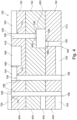
- FIG. 1 shows a spatial view of an electronic device 100 designed as a printed circuit board according to an exemplary embodiment of the invention.
- the electronic device 100 includes an electrically insulative support structure 102 formed from a mixture of glass fibers and epoxy resin.
- An electrically conductive conductor track 104 made of copper is formed on a surface of the carrier structure 102, more precisely in a groove in the surface of the carrier structure 102.
- the printed circuit board 104 can also protrude in a raised manner over a flat surface of the electrically insulating carrier structure 102 .
- an electrically conductive contact structure 106 made of copper is provided, which extends as a via, starting from the surface of the carrier structure 102, vertically into the carrier structure 102 and through the entire carrier structure 102 to an opposite one Surface of the support structure 102 extends.
- the contact structure 106 is directly or directly electrically connected to the conductor track 104 at a connection point 108 , forming a common conductor track 110 .
- the conductor track 104 and the contact structure 106 merge into one another without widening.
- a width or a thickness of the conductor track 104 on one side of the connection point 108 is equal to a width or a thickness of the contact structure 106 on the other side of the connection point 108.
- a diameter d of the contact structure 106 and the conductor track 104 is 30 in the exemplary embodiment shown ⁇ m.
- the connection point 108 is pad-free, that is to say it couples the contact structure 106 to the conductor track 104 directly and without a pad arranged in between.
- the conductor track 104 and the contact structure 106 have in the area of the connection point 108 and also along the entire extent of the conductor track 104 and the contact structure 106, a constant rectangular cross-section in terms of cross-sectional area and cross-sectional shape.
- connection point 108 In the area of the connection point 108, too, the conductor track 104 and the contact structure 106 are formed homogeneously from copper material, which is applied to the carrier structure 102 or introduced therein in a common method. The conductor track 104 and the contact structure 106 therefore merge into one another without any seams.
- the connection can also be referred to as "landless".
- FIG. 12 shows a cross-sectional view of the electronic device 100 of FIG figure 1 together with a schematically illustrated high-frequency signal, which propagates through a conductor line 110 of the device 100 .
- FIG. 12 it can be seen that the connection point 108 due to its homogeneity for the schematically illustrated high-frequency signal 200 represents practically no barrier, so that unwanted modes or other parasitic effects do not form at this point.
- the "landless" architecture is in accordance with Figure 1 and Figure 2 configured in such a way that it is particularly advantageous for the transport of high-frequency signals.
- figure 3 shows a top view of a conventional electronic device 300 with a pad 302 between a conductor track 304 and a via 306. Due to the mechanical inhomogeneity in the area of the transition between the conductor track 304 and the via 306 through the wide pad 302, conventional energy loss mechanisms occur in this area a propagating electrical signal, in particular a high-frequency signal.
- an in figure 3 likewise illustrated plan view of an electronic device 100 according to an exemplary embodiment of the invention, a pad-free and widening-free transition at a connection point 108 between a conductor track 104 and a via 106.
- figure 4 shows a cross-sectional view of an electronic device 100 designed as a multilayer interconnect according to an exemplary embodiment of the invention with embedded electronic components 400.
- the support structure 102 is formed from a plurality of dielectric layers 404 arranged one on top of the other, which can be formed, for example, from resin-impregnated glass fiber mats (prepreg material) and can be pressed together.
- the device 100 also includes another electrical conductive structure 402 in the form of a structured electrically conductive layer between the layers 404, which can also be pressed between the layers 404, for example.
- the device 100 has a plurality of conductor tracks 104 on the support structure 102 which are located on both opposite major surfaces 410, 412 of the support structure 102.
- the device 100 also has electronic components 400 which are embedded in the carrier structure 102 (“embedded components”) and are electrically conductively coupled to one of a plurality of vertical contact structures 106 and/or to one or more of horizontal conductor tracks 104 .
- Contact structures 106 and conductor tracks 104 are electrically conductively coupled to one another at respective connection points 108, forming a respective conductor track 110 without pads.
- an electrical contact 406 of the electronic component 400 and the contact structure 106 merge into one another without widening.
- an electrical contact 406 of the electronic component 400 and a respective conductor track 104 merge into one another without widening.
- One of the electronic components 400 is configured as a driver device that is used to couple in a high-frequency signal (see reference number 200 in figure 2 ) is formed in the connected trace 110, the high-frequency signal having a frequency of 500 GHz, for example.
- An edge steepness of the high-frequency signal is preferably greater than 200 V per 50 ps.
- the electronic component 400 embedded in the middle layer 404 can be used as the driving means for generating a high-frequency signal that is transmitted via the electronic contact 406 formed on the underside of the electronic component 400, a vertical contact structure 108, a on the underside of the device 100 arranged conductor track 104, a vertical contact structure 106, a arranged on the top of the device 100 conductor track 104, a further electrical contact 406 up to the exposed on the upper surface of the device 100 electronic component 400 (e.g. formed as a sensor). can. Since all transitions 108 are designed without broadening, the signal can propagate through the device 100 unhindered and thus without any loss of energy or quality.
- FIG. 7 shows an arrangement 700 that can be used during a method for manufacturing an electronic device 100 according to an exemplary embodiment of the invention.
- a groove 500 and a contact hole 502 are both formed by a common lithography process (see FIG figure 5 ) and etching process (see figure 6 ) educated.
- the carrier structure 102 can be arranged on a temporary carrier 706 during the performance of the lithography and etching process.
- a resist 702 is applied to the main surface 524 of the carrier structure 102 and structured by exposure using a mask. This defines an access opening 704 at which a subsequent etching process can attack material of the electrically insulating carrier structure 102 .
- an etching attack illustrated schematically with reference number 800, takes place, which selectively removes material of the carrier structure 102 by means of etching, which material is exposed at the access opening 704 and is not covered with the remaining resist 702.
- Etching can be performed, for example, by plasma etching, chemical etching, wet etching, or dry etching.
- the support structure 102 has an etch stop structure 708 formed from a material that remains protected from being removed by etching during the etching procedure.
- etchable material 710 of the electrically insulating carrier structure 102 can be removed during the etching process by means of etching. If the position of the etch stop structure 708 is known, the groove 500 and the contact opening 502 can be produced simultaneously with a single etching process in an exact position and without registration problems, and therefore without the need to provide pads to compensate for relative positional tolerances.
- figure 7 shows the arrangement 700 according to FIG Figure 5 and Figure 6 at a later time, when the groove 500 and the contact opening 502 are filled with electrically conductive material.
- the deposition method for depositing electrically conductive material see reference number 600, can be as per FIG figure 6 be performed.
- figure 8 shows an arrangement 1000 that can be used during yet another method for manufacturing an electronic device 100 according to an exemplary embodiment of the invention, in which a groove 500 and a contact opening 502 are formed in an electrically insulating carrier structure 102 by means of embossing (embossing), in which an electronic component 400 to be electrically contacted is already embedded.
- an embossing die 1002 is pressed onto the main surface 524 of the support structure 102 (see reference number 1020).
- the shape of the negative profile 1004 can be used to specify the shape of an embossing hole 1006 in the carrier structure 102 .
- the negative profile 1004 has a groove shape section 1008 for forming the groove 500 and a contact opening shape section 1010 for forming the contact opening 502 .
- an alignment marker 1030 for example a surface notch, can be provided on the carrier structure 102 in order to ensure, for example optically (see detector 1040), correct positioning of the die 1002 relative to the carrier body 102.
- a subsequent deposition method for depositing electrically conductive material can take place, for example, by means of sputtering, chemical vapor deposition, etc.
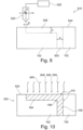
- FIG. 5 shows an arrangement 510 that can be used to carry out a method for producing an electronic device 100 according to an exemplary embodiment of the invention.
- a groove 500 running horizontally on a main surface 524 of an electrically insulating support structure 102 and a contact opening 502 extending vertically through the electrically insulating support structure 102 can be formed by means of laser grooving.
- a laser 520 which can be controlled by a control device 522 and can be moved along all three mutually orthogonal spatial directions (x, y and z) with a dwell time that can be set at a respective position along a specifiable trajectory along the main surface 524 of the electrically insulating support structure 102, is for forming of indentations formed in the main surface 524 of the electrically insulating structure 102 by means of laser grooving.
- the control device 522 processes a corresponding control program with which the laser 520 is moved along the specified trajectory and thus with an adjustable movement profile in the xy plane and remains in each position for a specified dwell time.
- a surface profile with a definable depth distribution can be generated, and a recess corresponding to or inverse to the conductor track 110 can also be formed as a result.
- the recess forms the groove 500 and the contact opening 502 which is directly adjacent to it and is therefore related to it Is contact opening 502, a precise definition of the shape of the groove 500 and the contact opening 502 is possible in a common procedure.
- figure 5 thus illustrates the performance of a first portion of a method for manufacturing an electronic device 100, wherein at an electrically insulating support structure 102 is initially provided as the starting structure for the method.
- the groove 500 is formed by removing material from the surface of the carrier structure 102 .
- the contact opening 502 extending into the carrier structure 102 is formed in a procedure common to the grooving.
- the groove 500 and the contact opening 502 are formed in a common, simultaneous, and non-disruptive procedure.
- the groove 500 and the contact opening 502 are subsequently, as in figure 10 shown filled with electrically conductive material to thereby form contact structure 106 .
- a procedure of defining a shape of the contact structure 106 seamlessly follows a procedure of defining a shape of the conductive line 104 (as an inverse of the groove 500). This advantageously eliminates the need to form a contact bridge in the form of a pad, as is conventionally required for two separate procedures, each with different tolerances, to compensate for registration problems.
- figure 10 shows the arrangement 510 according to FIG figure 9 at a later time, in which the groove 500 and the contact opening 502 are filled with electrically conductive material, to thereby form the conductor track 104 and the contact structure 106.
- the electrically conductive conductor track 104 is formed simultaneously on a surface of the carrier structure 102 and an electrically conductive contact structure 106 is formed, which, starting from the surface, extends into and under the carrier structure 102
- Forming a common conductor track 110 is electrically connected to the conductor track 104 at a connection point 108 .
- the conductor track 104 and the contact structure 106 merge into one another without widening and, also at the connection point 108, have a continuous or homogeneous material composition.
- the conductor track 104 and the contact structure 106 are formed in a joint, simultaneous and uninterrupted procedure.
- the material can be deposited, see reference number 600, for example by means of sputtering, chemical vapor deposition, etc.
Landscapes
- Engineering & Computer Science (AREA)
- Microelectronics & Electronic Packaging (AREA)
- Manufacturing & Machinery (AREA)
- Printing Elements For Providing Electric Connections Between Printed Circuits (AREA)
- Internal Circuitry In Semiconductor Integrated Circuit Devices (AREA)
Claims (13)
- Procédé de fabrication d'un dispositif électronique (100), le procédé comprenant les étapes consistant à :fournir une structure porteuse (102) électriquement isolante, la structure porteuse (102) comprend au moins un choisi dans le groupe constitué par : une plaque contenant une résine, un substrat en verre, un substrat organique ;former une piste électriquement conductrice (104) sur une surface de la structure porteuse (102) ;former une structure de contact électriquement conductrice (106) qui s'étend à l'intérieur de la structure porteuse (102) à partir de la surface, et qui est connectée électriquement à la piste conductrice (104) au niveau d'un point de connexion (108) de manière à former un chemin conducteur (110) commun,une ouverture de contact (502) s'étendant dans la structure porteuse (102) étant formée, qui est ensuite remplie d'un matériau électriquement conducteur, de manière à former la structure de contact (106), de sorte que la structure de contact (106) est réalisée sous la forme d'un trou borgne ou d'un trou traversant rempli du matériau électriquement conducteur dans la structure porteuse (102) ;la piste conductrice (104) et la structure de contact (106) étant réalisée se fondant l'une dans l'autre sans élargissement au niveau du point de connexion (108),caractérisé en ce quela piste conductrice (104) et la structure de contact (106) présentent une section transversale constante au moins dans la région du point de connexion (108) ; etune procédure de définition d'une configuration de la piste conductrice (104) et une procédure de définition d'une configuration de la structure de contact (106) sont consécutives sans interruption ou sont réalisées simultanément.
- Procédé selon la revendication 1, comprenant :
la piste conductrice (104) et la structure de contact (106) formées selon une procédure commune, en particulier simultanée ou sans interruption. - Procédé selon la revendication 1 ou 2, comprenant :
par l'intermédiaire du procédé, la formation d'une rainure (500) sur la surface de la structure porteuse (102) par enlèvement de matière, puis le remplissage du matériau électriquement conducteur pour former ainsi la piste conductrice (104). - Procédé selon l'une quelconque des revendications 1 à 3, comprenant au moins l'une des caractéristiques suivantes :au moins l'une de la rainure (500) et de l'ouverture de contact (502), de préférence les deux, est formée ou sont formées par un procédé de lithographie et de gravure ;au moins l'une de la rainure (500) et de l'ouverture de contact (502), de préférence les deux, est formée ou sont formées par estampage dans la structure porteuse (102) ;au moins l'une de la rainure (500) et de l'ouverture de contact (502), de préférence les deux, est formée ou sont formées au moyen d'un rainurage au laser.
- Procédé selon l'une quelconque des revendications 1 à 4, dans lequel le point de connexion (108) est exempt de pastille.
- Procédé selon l'une quelconque des revendications 1 à 5, dans lequel la piste conductrice (104) et la structure de contact (106) présentent une section transversale constante le long de toute l'étendue de la piste conductrice (104) et de la structure de contact (106).
- Procédé selon l'une quelconque des revendications 1 à 6, dans lequel la structure de contact (106) s'étend à l'intérieur de la structure porteuse (102) perpendiculairement à une extension de la piste conductrice (104) et se présente sous la forme d'une traversée.
- Procédé selon l'une quelconque des revendications 1 à 7,
dans lequel la piste conductrice (104) et la structure de contact (106) sont formées d'un matériau homogène au moins dans la région du point de connexion (108). - Procédé selon l'une quelconque des revendications 1 à 8, comprenant un composant électronique (400) qui est incorporé dans la structure porteuse (102) et couplé de manière électriquement conductrice à la structure de contact (106) et/ou à la piste conductrice (104), en particulier dans lequel le composant électronique (400) présente un composant haute fréquence.
- Procédé selon la revendication 9, dans lequel un contact électrique (406) du composant électronique (400), d'une part, et la structure de contact (106) ou la piste conductrice (104), d'autre part, se fondent l'une dans l'autre sans élargissement au niveau d'un autre point de connexion (108).
- Procédé selon l'une quelconque des revendications 1 à 10, présentant une autre piste conductrice (104) dans la structure porteuse (102), l'autre piste conductrice (104) et la structure de contact (106) se fondant l'une à l'autre sans élargissement au niveau d'un autre point de connexion (108).
- Procédé selon l'une quelconque des revendications précédentes, comprenant en outre l'étape consistant à :
fournir un dispositif de commande (400) conçu pour coupler un signal haute fréquence dans le chemin conducteur (110). - Procédé selon la revendication 12,
dans lequel le dispositif de commande (400) est conçu pour injecter un signal haute fréquence dans une plage de fréquence d'au moins 10 GHz.
Applications Claiming Priority (2)
| Application Number | Priority Date | Filing Date | Title |
|---|---|---|---|
| AT503392014 | 2014-05-14 | ||
| PCT/EP2015/060681 WO2015173347A1 (fr) | 2014-05-14 | 2015-05-13 | Chemin conducteur présentant une transition sans élargissement entre une piste conductrice et une structure de contact |
Publications (2)
| Publication Number | Publication Date |
|---|---|
| EP3143847A1 EP3143847A1 (fr) | 2017-03-22 |
| EP3143847B1 true EP3143847B1 (fr) | 2023-07-12 |
Family
ID=53276079
Family Applications (1)
| Application Number | Title | Priority Date | Filing Date |
|---|---|---|---|
| EP15726023.3A Active EP3143847B1 (fr) | 2014-05-14 | 2015-05-13 | Procede de fabriquer d'un chemin conducteur présentant une transition sans élargissement entre une piste conductrice et une structure de contact |
Country Status (4)
| Country | Link |
|---|---|
| US (2) | US10356904B2 (fr) |
| EP (1) | EP3143847B1 (fr) |
| CN (1) | CN106489305B (fr) |
| WO (1) | WO2015173347A1 (fr) |
Families Citing this family (2)
| Publication number | Priority date | Publication date | Assignee | Title |
|---|---|---|---|---|
| KR102678311B1 (ko) * | 2018-08-30 | 2024-06-25 | 삼성전자주식회사 | 패키지 볼을 갖는 반도체 패키지를 포함하는 전자 소자 |
| CN114521047B (zh) | 2020-11-19 | 2025-07-15 | 中兴通讯股份有限公司 | 一种印制电路板 |
Citations (3)
| Publication number | Priority date | Publication date | Assignee | Title |
|---|---|---|---|---|
| DE4343843A1 (de) * | 1993-12-22 | 1995-06-29 | Abb Patent Gmbh | Verfahren zur Herstellung strukturierter Metallisierungen |
| US20050196898A1 (en) * | 2004-03-02 | 2005-09-08 | Kwun-Yao Ho | Process of plating through hole |
| US20070222549A1 (en) * | 2006-02-21 | 2007-09-27 | Lim Michele H | Co-fired ceramic inductors with variable inductance, and voltage regulator having same |
Family Cites Families (20)
| Publication number | Priority date | Publication date | Assignee | Title |
|---|---|---|---|---|
| US4543715A (en) * | 1983-02-28 | 1985-10-01 | Allied Corporation | Method of forming vertical traces on printed circuit board |
| JPH09219468A (ja) | 1996-12-09 | 1997-08-19 | Shinko Electric Ind Co Ltd | 電子部品用基体 |
| TW519858B (en) | 2002-05-20 | 2003-02-01 | Via Tech Inc | Printing method for manufacturing through hole and circuit of circuit board |
| US7084354B2 (en) * | 2002-06-14 | 2006-08-01 | Intel Corporation | PCB method and apparatus for producing landless interconnects |
| EP2385041B1 (fr) * | 2003-05-01 | 2013-09-18 | Bristol-Myers Squibb Company | Composés de pyrazole-amines utilés en tant qu'inhibiteurs de kinase |
| TWI279177B (en) * | 2004-12-15 | 2007-04-11 | Mitac Int Corp | Manufacturing method of right-angled signal lines and the circuit board |
| US7204018B2 (en) * | 2004-12-16 | 2007-04-17 | Nortel Networks Limited | Technique for reducing via capacitance |
| US7158005B2 (en) | 2005-02-10 | 2007-01-02 | Harris Corporation | Embedded toroidal inductor |
| US7376799B2 (en) * | 2005-07-21 | 2008-05-20 | Hewlett-Packard Development Company, L.P. | System for reducing the latency of exclusive read requests in a symmetric multi-processing system |
| JP4620643B2 (ja) * | 2006-08-16 | 2011-01-26 | 富士通オプティカルコンポーネンツ株式会社 | インダクタ配線基板、インダクタ配線方法及びバイアスt回路 |
| JP2010103435A (ja) * | 2008-10-27 | 2010-05-06 | Shinko Electric Ind Co Ltd | 配線基板及びその製造方法 |
| TWI414223B (zh) * | 2010-01-21 | 2013-11-01 | Advanced Semiconductor Eng | 多引線通孔之形成方法 |
| DE102010010340B4 (de) * | 2010-03-04 | 2013-11-28 | Schneider Gmbh & Co. Kg | Messanordnung zum Vermessen eines Brillengestells |
| US9398694B2 (en) * | 2011-01-18 | 2016-07-19 | Sony Corporation | Method of manufacturing a package for embedding one or more electronic components |
| TWI445143B (zh) * | 2011-04-07 | 2014-07-11 | 欣興電子股份有限公司 | 封裝基板及其製法 |
| US8541884B2 (en) | 2011-07-06 | 2013-09-24 | Research Triangle Institute | Through-substrate via having a strip-shaped through-hole signal conductor |
| EP2605395A1 (fr) * | 2011-12-13 | 2013-06-19 | Bombardier Transportation GmbH | Inverseur de véhicule relié à des rails |
| KR20130085184A (ko) | 2012-01-19 | 2013-07-29 | 삼성전기주식회사 | 다층배선 구조물 및 그 제조방법 |
| US9144150B2 (en) * | 2012-04-20 | 2015-09-22 | Xilinx, Inc. | Conductor structure with integrated via element |
| JP5342704B1 (ja) * | 2012-11-12 | 2013-11-13 | 太陽誘電株式会社 | 高周波回路モジュール |
-
2015
- 2015-05-13 WO PCT/EP2015/060681 patent/WO2015173347A1/fr not_active Ceased
- 2015-05-13 EP EP15726023.3A patent/EP3143847B1/fr active Active
- 2015-05-13 US US15/310,991 patent/US10356904B2/en active Active
- 2015-05-13 CN CN201580038489.4A patent/CN106489305B/zh active Active
-
2019
- 2019-06-04 US US16/431,289 patent/US20190306983A1/en not_active Abandoned
Patent Citations (3)
| Publication number | Priority date | Publication date | Assignee | Title |
|---|---|---|---|---|
| DE4343843A1 (de) * | 1993-12-22 | 1995-06-29 | Abb Patent Gmbh | Verfahren zur Herstellung strukturierter Metallisierungen |
| US20050196898A1 (en) * | 2004-03-02 | 2005-09-08 | Kwun-Yao Ho | Process of plating through hole |
| US20070222549A1 (en) * | 2006-02-21 | 2007-09-27 | Lim Michele H | Co-fired ceramic inductors with variable inductance, and voltage regulator having same |
Also Published As
| Publication number | Publication date |
|---|---|
| US20190306983A1 (en) | 2019-10-03 |
| CN106489305A (zh) | 2017-03-08 |
| WO2015173347A1 (fr) | 2015-11-19 |
| US10356904B2 (en) | 2019-07-16 |
| EP3143847A1 (fr) | 2017-03-22 |
| US20170094795A1 (en) | 2017-03-30 |
| CN106489305B (zh) | 2020-02-28 |
Similar Documents
| Publication | Publication Date | Title |
|---|---|---|
| DE102019200893B4 (de) | Verfahren zum Erzeugen eines Hohlleiters, Schaltungsvorrichtung und Radarsystem | |
| DE2212735C3 (de) | Hochfrequenz-Übertragungsleitung in Streifenleiterbauweise | |
| DE69117381T2 (de) | Mehrschichtleiterplatte und Verfahren zu ihrer Herstellung | |
| DE112013001709B4 (de) | Elektronische Halbleiterbaugruppe für Millimeterwellen-Halbleiterplättchen | |
| DE69215192T2 (de) | Leiterplatte mit abgeschirmten bereichen sowie herstellungsverfahren einer solchen leiterplatte | |
| DE60320219T2 (de) | Aufteilung von strom-und erdungsebenen und durchkontaktverbindung zur nutzung von kanälen/gräben zur stromzufuhr | |
| DE69016441T2 (de) | Mehrschichtleiterplatte, welche hochfrequenzinterferenzen von hochfrequenzsignalen unterdrückt. | |
| DE112006003543T5 (de) | Eingebettete Wellenleiter-Leiterplatten-Struktur | |
| DE102020102362B4 (de) | Komponententräger mit Brückenstruktur in einem Durchgangsloch, das die Designregel für den Mindestabstand erfüllt | |
| DE2355471A1 (de) | Aus mehreren ebenen bestehende packung fuer halbleiterschaltungen | |
| DE102016212129B4 (de) | Hochfrequenz-Sende-/Empfangselement und Verfahren zur Herstellung eines Hochfrequenz-Sende-/Empfangselementes | |
| DE4020498C2 (de) | Verfahren zum Herstellen von Multiwire-Leiterplatten mit isolierten Metalleitern und/oder optischen Leitern | |
| EP3574722A1 (fr) | Procédé de réalisation d'un système électronique ou électrique et système réalisé par mise en oeuvre du procédé | |
| DE102022129321A1 (de) | Mehrschichtiges glassubstrat | |
| EP3903376B1 (fr) | Système de guide creux | |
| DE102013202806B4 (de) | Schaltung auf dünnem Träger für den Einsatz in Hohlleitern und Herstellungsverfahren | |
| DE112022000751T5 (de) | Glaspaketkern mit planaren strukturen | |
| EP3143847B1 (fr) | Procede de fabriquer d'un chemin conducteur présentant une transition sans élargissement entre une piste conductrice et une structure de contact | |
| EP0451541A1 (fr) | Fabrication de plaques de circuit multicouches à densité de conducteurs augmentée | |
| DE102023114910A1 (de) | Resonanzunterdrückung für Leistungs-Durchkontaktierungen | |
| DE60106510T2 (de) | Verbindungsstruktur für Übertragungsleitung, Hochfrequenzmodul und Übertragungsvorrichtung | |
| EP0710432B1 (fr) | Procede de fabrication de circuits imprimes en feuilles ou de produits semi-finis destines a la fabrication de circuits imprimes en feuilles, ainsi que circuits imprimes en feuilles et produits semi-finis fabriques selon ce procede | |
| DE112006003544T5 (de) | Leiterplattenaufbau mit einem Quasi-Wellenleiter | |
| DE102018215638B4 (de) | Bondfolie, elektronisches Bauelement und Verfahren zur Herstellung eines elektronischen Bauelements | |
| DE112006003395T5 (de) | Leiterplatten-Wellenleiter |
Legal Events
| Date | Code | Title | Description |
|---|---|---|---|
| STAA | Information on the status of an ep patent application or granted ep patent |
Free format text: STATUS: THE INTERNATIONAL PUBLICATION HAS BEEN MADE |
|
| PUAI | Public reference made under article 153(3) epc to a published international application that has entered the european phase |
Free format text: ORIGINAL CODE: 0009012 |
|
| STAA | Information on the status of an ep patent application or granted ep patent |
Free format text: STATUS: REQUEST FOR EXAMINATION WAS MADE |
|
| 17P | Request for examination filed |
Effective date: 20161209 |
|
| AK | Designated contracting states |
Kind code of ref document: A1 Designated state(s): AL AT BE BG CH CY CZ DE DK EE ES FI FR GB GR HR HU IE IS IT LI LT LU LV MC MK MT NL NO PL PT RO RS SE SI SK SM TR |
|
| AX | Request for extension of the european patent |
Extension state: BA ME |
|
| DAV | Request for validation of the european patent (deleted) | ||
| DAX | Request for extension of the european patent (deleted) | ||
| STAA | Information on the status of an ep patent application or granted ep patent |
Free format text: STATUS: EXAMINATION IS IN PROGRESS |
|
| 17Q | First examination report despatched |
Effective date: 20190103 |
|
| GRAP | Despatch of communication of intention to grant a patent |
Free format text: ORIGINAL CODE: EPIDOSNIGR1 |
|
| STAA | Information on the status of an ep patent application or granted ep patent |
Free format text: STATUS: GRANT OF PATENT IS INTENDED |
|
| INTG | Intention to grant announced |
Effective date: 20230124 |
|
| GRAS | Grant fee paid |
Free format text: ORIGINAL CODE: EPIDOSNIGR3 |
|
| GRAA | (expected) grant |
Free format text: ORIGINAL CODE: 0009210 |
|
| STAA | Information on the status of an ep patent application or granted ep patent |
Free format text: STATUS: THE PATENT HAS BEEN GRANTED |
|
| AK | Designated contracting states |
Kind code of ref document: B1 Designated state(s): AL AT BE BG CH CY CZ DE DK EE ES FI FR GB GR HR HU IE IS IT LI LT LU LV MC MK MT NL NO PL PT RO RS SE SI SK SM TR |
|
| REG | Reference to a national code |
Ref country code: CH Ref legal event code: EP |
|
| P01 | Opt-out of the competence of the unified patent court (upc) registered |
Effective date: 20230620 |
|
| REG | Reference to a national code |
Ref country code: DE Ref legal event code: R096 Ref document number: 502015016488 Country of ref document: DE |
|
| REG | Reference to a national code |
Ref country code: IE Ref legal event code: FG4D Free format text: LANGUAGE OF EP DOCUMENT: GERMAN |
|
| REG | Reference to a national code |
Ref country code: LT Ref legal event code: MG9D |
|
| REG | Reference to a national code |
Ref country code: NL Ref legal event code: MP Effective date: 20230712 |
|
| PG25 | Lapsed in a contracting state [announced via postgrant information from national office to epo] |
Ref country code: NL Free format text: LAPSE BECAUSE OF FAILURE TO SUBMIT A TRANSLATION OF THE DESCRIPTION OR TO PAY THE FEE WITHIN THE PRESCRIBED TIME-LIMIT Effective date: 20230712 |
|
| PG25 | Lapsed in a contracting state [announced via postgrant information from national office to epo] |
Ref country code: GR Free format text: LAPSE BECAUSE OF FAILURE TO SUBMIT A TRANSLATION OF THE DESCRIPTION OR TO PAY THE FEE WITHIN THE PRESCRIBED TIME-LIMIT Effective date: 20231013 |
|
| PG25 | Lapsed in a contracting state [announced via postgrant information from national office to epo] |
Ref country code: ES Free format text: LAPSE BECAUSE OF FAILURE TO SUBMIT A TRANSLATION OF THE DESCRIPTION OR TO PAY THE FEE WITHIN THE PRESCRIBED TIME-LIMIT Effective date: 20230712 |
|
| PG25 | Lapsed in a contracting state [announced via postgrant information from national office to epo] |
Ref country code: IS Free format text: LAPSE BECAUSE OF FAILURE TO SUBMIT A TRANSLATION OF THE DESCRIPTION OR TO PAY THE FEE WITHIN THE PRESCRIBED TIME-LIMIT Effective date: 20231112 |
|
| PG25 | Lapsed in a contracting state [announced via postgrant information from national office to epo] |
Ref country code: SE Free format text: LAPSE BECAUSE OF FAILURE TO SUBMIT A TRANSLATION OF THE DESCRIPTION OR TO PAY THE FEE WITHIN THE PRESCRIBED TIME-LIMIT Effective date: 20230712 Ref country code: RS Free format text: LAPSE BECAUSE OF FAILURE TO SUBMIT A TRANSLATION OF THE DESCRIPTION OR TO PAY THE FEE WITHIN THE PRESCRIBED TIME-LIMIT Effective date: 20230712 Ref country code: PT Free format text: LAPSE BECAUSE OF FAILURE TO SUBMIT A TRANSLATION OF THE DESCRIPTION OR TO PAY THE FEE WITHIN THE PRESCRIBED TIME-LIMIT Effective date: 20231113 Ref country code: NO Free format text: LAPSE BECAUSE OF FAILURE TO SUBMIT A TRANSLATION OF THE DESCRIPTION OR TO PAY THE FEE WITHIN THE PRESCRIBED TIME-LIMIT Effective date: 20231012 Ref country code: LV Free format text: LAPSE BECAUSE OF FAILURE TO SUBMIT A TRANSLATION OF THE DESCRIPTION OR TO PAY THE FEE WITHIN THE PRESCRIBED TIME-LIMIT Effective date: 20230712 Ref country code: LT Free format text: LAPSE BECAUSE OF FAILURE TO SUBMIT A TRANSLATION OF THE DESCRIPTION OR TO PAY THE FEE WITHIN THE PRESCRIBED TIME-LIMIT Effective date: 20230712 Ref country code: IS Free format text: LAPSE BECAUSE OF FAILURE TO SUBMIT A TRANSLATION OF THE DESCRIPTION OR TO PAY THE FEE WITHIN THE PRESCRIBED TIME-LIMIT Effective date: 20231112 Ref country code: HR Free format text: LAPSE BECAUSE OF FAILURE TO SUBMIT A TRANSLATION OF THE DESCRIPTION OR TO PAY THE FEE WITHIN THE PRESCRIBED TIME-LIMIT Effective date: 20230712 Ref country code: GR Free format text: LAPSE BECAUSE OF FAILURE TO SUBMIT A TRANSLATION OF THE DESCRIPTION OR TO PAY THE FEE WITHIN THE PRESCRIBED TIME-LIMIT Effective date: 20231013 Ref country code: FI Free format text: LAPSE BECAUSE OF FAILURE TO SUBMIT A TRANSLATION OF THE DESCRIPTION OR TO PAY THE FEE WITHIN THE PRESCRIBED TIME-LIMIT Effective date: 20230712 Ref country code: ES Free format text: LAPSE BECAUSE OF FAILURE TO SUBMIT A TRANSLATION OF THE DESCRIPTION OR TO PAY THE FEE WITHIN THE PRESCRIBED TIME-LIMIT Effective date: 20230712 |
|
| PG25 | Lapsed in a contracting state [announced via postgrant information from national office to epo] |
Ref country code: PL Free format text: LAPSE BECAUSE OF FAILURE TO SUBMIT A TRANSLATION OF THE DESCRIPTION OR TO PAY THE FEE WITHIN THE PRESCRIBED TIME-LIMIT Effective date: 20230712 |
|
| REG | Reference to a national code |
Ref country code: DE Ref legal event code: R097 Ref document number: 502015016488 Country of ref document: DE |
|
| PG25 | Lapsed in a contracting state [announced via postgrant information from national office to epo] |
Ref country code: SM Free format text: LAPSE BECAUSE OF FAILURE TO SUBMIT A TRANSLATION OF THE DESCRIPTION OR TO PAY THE FEE WITHIN THE PRESCRIBED TIME-LIMIT Effective date: 20230712 Ref country code: RO Free format text: LAPSE BECAUSE OF FAILURE TO SUBMIT A TRANSLATION OF THE DESCRIPTION OR TO PAY THE FEE WITHIN THE PRESCRIBED TIME-LIMIT Effective date: 20230712 Ref country code: EE Free format text: LAPSE BECAUSE OF FAILURE TO SUBMIT A TRANSLATION OF THE DESCRIPTION OR TO PAY THE FEE WITHIN THE PRESCRIBED TIME-LIMIT Effective date: 20230712 Ref country code: DK Free format text: LAPSE BECAUSE OF FAILURE TO SUBMIT A TRANSLATION OF THE DESCRIPTION OR TO PAY THE FEE WITHIN THE PRESCRIBED TIME-LIMIT Effective date: 20230712 Ref country code: CZ Free format text: LAPSE BECAUSE OF FAILURE TO SUBMIT A TRANSLATION OF THE DESCRIPTION OR TO PAY THE FEE WITHIN THE PRESCRIBED TIME-LIMIT Effective date: 20230712 Ref country code: SK Free format text: LAPSE BECAUSE OF FAILURE TO SUBMIT A TRANSLATION OF THE DESCRIPTION OR TO PAY THE FEE WITHIN THE PRESCRIBED TIME-LIMIT Effective date: 20230712 |
|
| PLBE | No opposition filed within time limit |
Free format text: ORIGINAL CODE: 0009261 |
|
| STAA | Information on the status of an ep patent application or granted ep patent |
Free format text: STATUS: NO OPPOSITION FILED WITHIN TIME LIMIT |
|
| PG25 | Lapsed in a contracting state [announced via postgrant information from national office to epo] |
Ref country code: IT Free format text: LAPSE BECAUSE OF FAILURE TO SUBMIT A TRANSLATION OF THE DESCRIPTION OR TO PAY THE FEE WITHIN THE PRESCRIBED TIME-LIMIT Effective date: 20230712 |
|
| 26N | No opposition filed |
Effective date: 20240415 |
|
| PG25 | Lapsed in a contracting state [announced via postgrant information from national office to epo] |
Ref country code: SI Free format text: LAPSE BECAUSE OF FAILURE TO SUBMIT A TRANSLATION OF THE DESCRIPTION OR TO PAY THE FEE WITHIN THE PRESCRIBED TIME-LIMIT Effective date: 20230712 |
|
| PG25 | Lapsed in a contracting state [announced via postgrant information from national office to epo] |
Ref country code: BG Free format text: LAPSE BECAUSE OF FAILURE TO SUBMIT A TRANSLATION OF THE DESCRIPTION OR TO PAY THE FEE WITHIN THE PRESCRIBED TIME-LIMIT Effective date: 20230712 |
|
| PG25 | Lapsed in a contracting state [announced via postgrant information from national office to epo] |
Ref country code: BG Free format text: LAPSE BECAUSE OF FAILURE TO SUBMIT A TRANSLATION OF THE DESCRIPTION OR TO PAY THE FEE WITHIN THE PRESCRIBED TIME-LIMIT Effective date: 20230712 |
|
| REG | Reference to a national code |
Ref country code: CH Ref legal event code: PL |
|
| PG25 | Lapsed in a contracting state [announced via postgrant information from national office to epo] |
Ref country code: MC Free format text: LAPSE BECAUSE OF FAILURE TO SUBMIT A TRANSLATION OF THE DESCRIPTION OR TO PAY THE FEE WITHIN THE PRESCRIBED TIME-LIMIT Effective date: 20230712 |
|
| PG25 | Lapsed in a contracting state [announced via postgrant information from national office to epo] |
Ref country code: LU Free format text: LAPSE BECAUSE OF NON-PAYMENT OF DUE FEES Effective date: 20240513 |
|
| GBPC | Gb: european patent ceased through non-payment of renewal fee |
Effective date: 20240513 |
|
| PG25 | Lapsed in a contracting state [announced via postgrant information from national office to epo] |
Ref country code: MC Free format text: LAPSE BECAUSE OF FAILURE TO SUBMIT A TRANSLATION OF THE DESCRIPTION OR TO PAY THE FEE WITHIN THE PRESCRIBED TIME-LIMIT Effective date: 20230712 Ref country code: LU Free format text: LAPSE BECAUSE OF NON-PAYMENT OF DUE FEES Effective date: 20240513 Ref country code: CH Free format text: LAPSE BECAUSE OF NON-PAYMENT OF DUE FEES Effective date: 20240531 |
|
| REG | Reference to a national code |
Ref country code: BE Ref legal event code: MM Effective date: 20240531 |
|
| PG25 | Lapsed in a contracting state [announced via postgrant information from national office to epo] |
Ref country code: IE Free format text: LAPSE BECAUSE OF NON-PAYMENT OF DUE FEES Effective date: 20240513 |
|
| PG25 | Lapsed in a contracting state [announced via postgrant information from national office to epo] |
Ref country code: BE Free format text: LAPSE BECAUSE OF NON-PAYMENT OF DUE FEES Effective date: 20240531 |
|
| PG25 | Lapsed in a contracting state [announced via postgrant information from national office to epo] |
Ref country code: GB Free format text: LAPSE BECAUSE OF NON-PAYMENT OF DUE FEES Effective date: 20240513 |
|
| PGFP | Annual fee paid to national office [announced via postgrant information from national office to epo] |
Ref country code: DE Payment date: 20250523 Year of fee payment: 11 |
|
| REG | Reference to a national code |
Ref country code: AT Ref legal event code: MM01 Ref document number: 1588454 Country of ref document: AT Kind code of ref document: T Effective date: 20240513 |
|
| PGFP | Annual fee paid to national office [announced via postgrant information from national office to epo] |
Ref country code: FR Payment date: 20250526 Year of fee payment: 11 |
|
| PG25 | Lapsed in a contracting state [announced via postgrant information from national office to epo] |
Ref country code: AT Free format text: LAPSE BECAUSE OF NON-PAYMENT OF DUE FEES Effective date: 20240513 |
|
| PG25 | Lapsed in a contracting state [announced via postgrant information from national office to epo] |
Ref country code: CY Free format text: LAPSE BECAUSE OF FAILURE TO SUBMIT A TRANSLATION OF THE DESCRIPTION OR TO PAY THE FEE WITHIN THE PRESCRIBED TIME-LIMIT; INVALID AB INITIO Effective date: 20150513 |
|
| PG25 | Lapsed in a contracting state [announced via postgrant information from national office to epo] |
Ref country code: HU Free format text: LAPSE BECAUSE OF FAILURE TO SUBMIT A TRANSLATION OF THE DESCRIPTION OR TO PAY THE FEE WITHIN THE PRESCRIBED TIME-LIMIT; INVALID AB INITIO Effective date: 20150513 |