EP3190672A1 - Laserquelle mit halbleiter - Google Patents
Laserquelle mit halbleiter Download PDFInfo
- Publication number
- EP3190672A1 EP3190672A1 EP17150156.2A EP17150156A EP3190672A1 EP 3190672 A1 EP3190672 A1 EP 3190672A1 EP 17150156 A EP17150156 A EP 17150156A EP 3190672 A1 EP3190672 A1 EP 3190672A1
- Authority
- EP
- European Patent Office
- Prior art keywords
- waveguide
- filter
- laser source
- silicon
- wavelength
- Prior art date
- Legal status (The legal status is an assumption and is not a legal conclusion. Google has not performed a legal analysis and makes no representation as to the accuracy of the status listed.)
- Granted
Links
Images




Classifications
-
- H—ELECTRICITY
- H01—ELECTRIC ELEMENTS
- H01S—DEVICES USING THE PROCESS OF LIGHT AMPLIFICATION BY STIMULATED EMISSION OF RADIATION [LASER] TO AMPLIFY OR GENERATE LIGHT; DEVICES USING STIMULATED EMISSION OF ELECTROMAGNETIC RADIATION IN WAVE RANGES OTHER THAN OPTICAL
- H01S5/00—Semiconductor lasers
- H01S5/06—Arrangements for controlling the laser output parameters, e.g. by operating on the active medium
- H01S5/068—Stabilisation of laser output parameters
- H01S5/0683—Stabilisation of laser output parameters by monitoring the optical output parameters
- H01S5/0687—Stabilising the frequency of the laser
-
- H—ELECTRICITY
- H01—ELECTRIC ELEMENTS
- H01S—DEVICES USING THE PROCESS OF LIGHT AMPLIFICATION BY STIMULATED EMISSION OF RADIATION [LASER] TO AMPLIFY OR GENERATE LIGHT; DEVICES USING STIMULATED EMISSION OF ELECTROMAGNETIC RADIATION IN WAVE RANGES OTHER THAN OPTICAL
- H01S5/00—Semiconductor lasers
- H01S5/02—Structural details or components not essential to laser action
- H01S5/0206—Substrates, e.g. growth, shape, material, removal or bonding
- H01S5/021—Silicon based substrates
-
- H—ELECTRICITY
- H01—ELECTRIC ELEMENTS
- H01S—DEVICES USING THE PROCESS OF LIGHT AMPLIFICATION BY STIMULATED EMISSION OF RADIATION [LASER] TO AMPLIFY OR GENERATE LIGHT; DEVICES USING STIMULATED EMISSION OF ELECTROMAGNETIC RADIATION IN WAVE RANGES OTHER THAN OPTICAL
- H01S5/00—Semiconductor lasers
- H01S5/02—Structural details or components not essential to laser action
- H01S5/026—Monolithically integrated components, e.g. waveguides, monitoring photo-detectors, drivers
-
- H—ELECTRICITY
- H01—ELECTRIC ELEMENTS
- H01S—DEVICES USING THE PROCESS OF LIGHT AMPLIFICATION BY STIMULATED EMISSION OF RADIATION [LASER] TO AMPLIFY OR GENERATE LIGHT; DEVICES USING STIMULATED EMISSION OF ELECTROMAGNETIC RADIATION IN WAVE RANGES OTHER THAN OPTICAL
- H01S5/00—Semiconductor lasers
- H01S5/06—Arrangements for controlling the laser output parameters, e.g. by operating on the active medium
- H01S5/062—Arrangements for controlling the laser output parameters, e.g. by operating on the active medium by varying the potential of the electrodes
- H01S5/0625—Arrangements for controlling the laser output parameters, e.g. by operating on the active medium by varying the potential of the electrodes in multi-section lasers
- H01S5/06255—Controlling the frequency of the radiation
-
- H—ELECTRICITY
- H01—ELECTRIC ELEMENTS
- H01S—DEVICES USING THE PROCESS OF LIGHT AMPLIFICATION BY STIMULATED EMISSION OF RADIATION [LASER] TO AMPLIFY OR GENERATE LIGHT; DEVICES USING STIMULATED EMISSION OF ELECTROMAGNETIC RADIATION IN WAVE RANGES OTHER THAN OPTICAL
- H01S5/00—Semiconductor lasers
- H01S5/10—Construction or shape of the optical resonator, e.g. extended or external cavity, coupled cavities, bent-guide, varying width, thickness or composition of the active region
- H01S5/1028—Coupling to elements in the cavity, e.g. coupling to waveguides adjacent the active region, e.g. forward coupled [DFC] structures
-
- H—ELECTRICITY
- H01—ELECTRIC ELEMENTS
- H01S—DEVICES USING THE PROCESS OF LIGHT AMPLIFICATION BY STIMULATED EMISSION OF RADIATION [LASER] TO AMPLIFY OR GENERATE LIGHT; DEVICES USING STIMULATED EMISSION OF ELECTROMAGNETIC RADIATION IN WAVE RANGES OTHER THAN OPTICAL
- H01S5/00—Semiconductor lasers
- H01S5/10—Construction or shape of the optical resonator, e.g. extended or external cavity, coupled cavities, bent-guide, varying width, thickness or composition of the active region
- H01S5/1028—Coupling to elements in the cavity, e.g. coupling to waveguides adjacent the active region, e.g. forward coupled [DFC] structures
- H01S5/1032—Coupling to elements comprising an optical axis that is not aligned with the optical axis of the active region
-
- H—ELECTRICITY
- H01—ELECTRIC ELEMENTS
- H01S—DEVICES USING THE PROCESS OF LIGHT AMPLIFICATION BY STIMULATED EMISSION OF RADIATION [LASER] TO AMPLIFY OR GENERATE LIGHT; DEVICES USING STIMULATED EMISSION OF ELECTROMAGNETIC RADIATION IN WAVE RANGES OTHER THAN OPTICAL
- H01S5/00—Semiconductor lasers
- H01S5/10—Construction or shape of the optical resonator, e.g. extended or external cavity, coupled cavities, bent-guide, varying width, thickness or composition of the active region
- H01S5/1071—Ring-lasers
-
- H—ELECTRICITY
- H01—ELECTRIC ELEMENTS
- H01S—DEVICES USING THE PROCESS OF LIGHT AMPLIFICATION BY STIMULATED EMISSION OF RADIATION [LASER] TO AMPLIFY OR GENERATE LIGHT; DEVICES USING STIMULATED EMISSION OF ELECTROMAGNETIC RADIATION IN WAVE RANGES OTHER THAN OPTICAL
- H01S5/00—Semiconductor lasers
- H01S5/10—Construction or shape of the optical resonator, e.g. extended or external cavity, coupled cavities, bent-guide, varying width, thickness or composition of the active region
- H01S5/1092—Multi-wavelength lasing
-
- H—ELECTRICITY
- H01—ELECTRIC ELEMENTS
- H01S—DEVICES USING THE PROCESS OF LIGHT AMPLIFICATION BY STIMULATED EMISSION OF RADIATION [LASER] TO AMPLIFY OR GENERATE LIGHT; DEVICES USING STIMULATED EMISSION OF ELECTROMAGNETIC RADIATION IN WAVE RANGES OTHER THAN OPTICAL
- H01S5/00—Semiconductor lasers
- H01S5/10—Construction or shape of the optical resonator, e.g. extended or external cavity, coupled cavities, bent-guide, varying width, thickness or composition of the active region
- H01S5/14—External cavity lasers
-
- H—ELECTRICITY
- H01—ELECTRIC ELEMENTS
- H01S—DEVICES USING THE PROCESS OF LIGHT AMPLIFICATION BY STIMULATED EMISSION OF RADIATION [LASER] TO AMPLIFY OR GENERATE LIGHT; DEVICES USING STIMULATED EMISSION OF ELECTROMAGNETIC RADIATION IN WAVE RANGES OTHER THAN OPTICAL
- H01S5/00—Semiconductor lasers
- H01S5/10—Construction or shape of the optical resonator, e.g. extended or external cavity, coupled cavities, bent-guide, varying width, thickness or composition of the active region
- H01S5/14—External cavity lasers
- H01S5/141—External cavity lasers using a wavelength selective device, e.g. a grating or etalon
-
- H—ELECTRICITY
- H01—ELECTRIC ELEMENTS
- H01S—DEVICES USING THE PROCESS OF LIGHT AMPLIFICATION BY STIMULATED EMISSION OF RADIATION [LASER] TO AMPLIFY OR GENERATE LIGHT; DEVICES USING STIMULATED EMISSION OF ELECTROMAGNETIC RADIATION IN WAVE RANGES OTHER THAN OPTICAL
- H01S5/00—Semiconductor lasers
- H01S5/10—Construction or shape of the optical resonator, e.g. extended or external cavity, coupled cavities, bent-guide, varying width, thickness or composition of the active region
- H01S5/14—External cavity lasers
- H01S5/141—External cavity lasers using a wavelength selective device, e.g. a grating or etalon
- H01S5/142—External cavity lasers using a wavelength selective device, e.g. a grating or etalon which comprises an additional resonator
-
- H—ELECTRICITY
- H01—ELECTRIC ELEMENTS
- H01S—DEVICES USING THE PROCESS OF LIGHT AMPLIFICATION BY STIMULATED EMISSION OF RADIATION [LASER] TO AMPLIFY OR GENERATE LIGHT; DEVICES USING STIMULATED EMISSION OF ELECTROMAGNETIC RADIATION IN WAVE RANGES OTHER THAN OPTICAL
- H01S5/00—Semiconductor lasers
- H01S5/20—Structure or shape of the semiconductor body to guide the optical wave ; Confining structures perpendicular to the optical axis, e.g. index or gain guiding, stripe geometry, broad area lasers, gain tailoring, transverse or lateral reflectors, special cladding structures, MQW barrier reflection layers
- H01S5/2004—Confining in the direction perpendicular to the layer structure
- H01S5/2018—Optical confinement, e.g. absorbing-, reflecting- or waveguide-layers
- H01S5/2031—Optical confinement, e.g. absorbing-, reflecting- or waveguide-layers characterized by special waveguide layers, e.g. asymmetric waveguide layers or defined bandgap discontinuities
-
- H—ELECTRICITY
- H01—ELECTRIC ELEMENTS
- H01S—DEVICES USING THE PROCESS OF LIGHT AMPLIFICATION BY STIMULATED EMISSION OF RADIATION [LASER] TO AMPLIFY OR GENERATE LIGHT; DEVICES USING STIMULATED EMISSION OF ELECTROMAGNETIC RADIATION IN WAVE RANGES OTHER THAN OPTICAL
- H01S5/00—Semiconductor lasers
- H01S5/30—Structure or shape of the active region; Materials used for the active region
- H01S5/3013—AIIIBV compounds
Definitions
- the invention relates to a semiconductor laser source capable of emitting at least one wavelength ⁇ Li , as well as a method of manufacturing this laser source.
- the filter and the reflectors are made in silicon waveguides and the filter selects only a single wavelength.
- the emission wavelength of these laser sources also varies at about 0.07 nm / ° C. Because of this, it is said that these known laser sources are temperature sensitive and that the emission wavelength of the laser source drifts as a function of temperature.
- the invention aims to overcome this disadvantage by providing a semiconductor laser source less sensitive to temperature variations while remaining simple to manufacture. It therefore relates to a semiconductor laser source according to claim 1.
- the proposed solution consists in producing the filter in a waveguide, no longer made of silicon but in a material that is less sensitive to temperature, and integrating this filter with the structure of the laser source.
- the waveguide in which the filter is made is in a material whose variation of the refractive index as a function of the temperature is at least two times slower than the variation of the index of Refraction of the silicon makes it possible to limit the drift in temperature of the filter.
- the tuning device, the sensor and the electronic circuit make it possible to permanently maintain a wavelength ⁇ Rj in the center of each bandwidth of the filter which selects a wavelength ⁇ Li . This has the consequence of reducing the amplitude of the temperature drift of the emission wavelength ⁇ Li of the laser source without the need to resort to a device for regulating the temperature of the source laser.
- the integration into the laser source of this filter is made possible by the implementation of a laser source structure with three waveguides, namely a silicon waveguide, a waveguide made of III-V gain and a waveguide made of a material less sensitive to temperature.
- This structure with three waveguides in particular makes it possible to circumvent the difficulty that it is difficult to perform an adiabatic coupling directly between the waveguide of less temperature-sensitive material and the waveguide of gain material. V. Indeed, the materials of these two waveguides generally have large differences in optical refractive index.
- a silicon waveguide to couple, on the one hand, the waveguide of III-V gain material to the silicon waveguide and, d on the other hand, the silicon waveguide to the waveguide of less temperature sensitive material.
- waveguides made of III-V gain material and less temperature-sensitive material are coupled to one another. to the other via the silicon waveguide.
- the presence of the silicon waveguide can be used to make a particularly efficient tuning device. Indeed, the variation of the refractive index of silicon as a function of temperature is important and it is also possible to simply generate free carriers in a silicon waveguide. These two phenomena modify the phase of the optical signal that propagates in the silicon waveguide.
- Embodiments of this laser source may have one or more of the features of the dependent claims.
- the invention also relates to a method of manufacturing the claimed laser source.
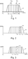
- the figure 1 represents a reflective band 4 of the front and rear reflectors of a Fabry-Perot optical cavity of a known semiconductor laser source.
- This bandwidth 4 is represented on a graph where the abscissa axis represents the wavelength and is expressed in nanometers and the ordinate axis corresponds to the power of the optical signal expressed in watts.
- the reflective band 4 is characterized by its width ⁇ R and its central wavelength ⁇ CR .
- the width ⁇ R is the width of the reflective band 4 at -3 dB. This is the wavelength band containing all the wavelengths ⁇ Rj capable of being reflected by the front and rear reflectors with a power greater than or equal to 50% of the maximum power I max reflected by these reflectors. .
- the power I max is equal to the power of the reflected optical signal for the wavelength ⁇ Rj for which this power is maximum.
- the ⁇ CR center wavelength is the wavelength in the middle of the reflective band 4.
- the different wavelengths ⁇ Rj at which this cavity is likely to resonate are regularly spaced from each other by an interval ⁇ R.
- the wavelengths ⁇ Rj at which the Fabry-Perot cavity can resonate and which are located inside the bandwidth 4 are represented by vertical lines.
- the filter selects from among the set of possible wavelengths ⁇ Rj only one of these lengths ⁇ Rj .
- the wavelength ⁇ Rj selected is equal to the wavelength ⁇ Li emission of the laser source.
- the filter has a single narrow bandwidth 6 centered on the wavelength ⁇ Li .
- This bandwidth 6 is characterized by its width ⁇ f and its central wavelength ⁇ Cf.
- the width ⁇ f is the width of the bandwidth 6 at -3 dB.
- the central wavelength ⁇ Cf is the wavelength located in the middle of the passband 6.
- the width ⁇ f is less than or equal to the interval ⁇ R.
- one of the wavelengths ⁇ Rj is tuned to be equal to this wavelength ⁇ Cf.
- This wavelength ⁇ Rj which is equal to the wavelength ⁇ Cf corresponds to the wavelength ⁇ Li .
- the graph of the figure 1 is shown for an operating temperature of the laser source equal to 20 ° C.
- the optical signal is guided between the front and rear reflectors by silicon waveguides and III-V gain materials.
- the reflectors and the filter are made in the silicon waveguides, and the gain function is performed in the III-V material waveguide.
- the wavelengths ⁇ Rj and the wavelength ⁇ CR are displaced as a function of the temperature of approximately 0.07 nm / ° C.
- the wavelength ⁇ Cf also moves about 0.07 nm / ° C.
- the graph of the figure 2 represents the same elements as the graph of the figure 1 , but for an operating temperature of the laser source equal to 33 ° C. It can be seen that the bandwidth 4 and the wavelengths ⁇ CR and ⁇ Rj have shifted by about 0.9 nm (approximately 0.07 x 13 ° C) and that the bandwidth 6 has moved from approximately 0.9 nm. The wavelength ⁇ Li of the laser source has therefore moved about 0.9 nm.
- the proposed solution consists in producing the filter in a waveguide, no longer in silicon but in a dielectric material that is less sensitive to temperature, and integrating such a filter into the structure of a laser source.
- a material less sensitive to temperature is a material whose variation dn f / dT of its refractive index as a function of temperature is at least two times lower, under the same conditions, with the variation dn Si / dT of the refractive index of silicon as a function of temperature.
- the variation dn Si / dT is equal to 2.3 x 10 -4 / ° C to plus or minus 20%.
- the variation dn f / dT is at least less than 1 x 10 -4 / ° C and, preferably, less than 0.5 x 10 -4 / ° C.
- the material less sensitive to temperature is silicon nitride (Si 3 N 4 ) whose variation dn f / dT is equal to 0.4 x 10 -4 / ° C.
- silicon nitride Si 3 N 4
- the refractive index of silicon nitride varies with the temperature six to seven times slower than that of silicon. Consequently, the central wavelength ⁇ Cf of the filter produced in a silicon nitride waveguide moves, as a function of temperature, only 0.01 nm / ° C.
- the figure 3 represents the position of the reflective band 4 and the bandwidth 6 in the case where the filter is made in a silicon nitride waveguide and for an operating temperature of the laser source of 33 ° C.
- the amplitude of the displacement of the central wavelength ⁇ CR is the same as in the case represented on the figure 2 .
- the fact of only making the filter in a material less sensitive to temperature is already sufficient to very strongly limit the sensitivity of the wavelength ⁇ Cf to the temperature. Since it is the filter that selects the wavelength ⁇ Li of emission of the laser source, it becomes possible, after centering a wavelength ⁇ Rj on the wavelength ⁇ Cf to obtain a wavelength ⁇ Li d emission of the laser source less sensitive to temperature.
- a tuning device, a sensor and an electronic control circuit are used to automatically and correctly center the nearest wavelength ⁇ Rj in the center of the bandête 6 of the filter to obtain the emission of the laser source on the wavelength ⁇ Li .
- this bandwidth 6 may contain no wavelength ⁇ Rj or wavelength ⁇ Rj misaligned which eliminates the emission of the laser source or strongly limits the power of the optical signal emitted.
- the figure 4 schematically represents the general architecture of a monochromatic semiconductor laser source 10 which emits at the wavelength ⁇ Li .
- the laser source 10 includes a rear reflector 12 and a front reflector 14 which define the ends of the Fabry-Perot cavity within which the optical signal resonates.
- the reflector 12 has a reflection factor strictly greater than that of the reflector 14.
- the reflection factor is equal to the ratio between the power of the optical signal reflected by the reflector on the power of the optical signal incident on this reflector.
- the reflection factor of the reflector 12 is greater than or equal to 90% or 95% for the wavelength ⁇ Li .
- the reflection factor of the reflector 14 is generally between 30% and 70% and is typically 50%.
- the operating temperature range of a laser source is nowadays often chosen so that, regardless of the operating temperature of the laser source located inside this range, this does not cause a variation in the length of the laser.
- the width DT of this range is greater than 10 ° C or 30 ° C.
- the operating temperature range is chosen to be between + 20 ° C and + 55 ° C.
- the width DT is here equal to 35 ° C.
- the smallest and the largest temperatures of the operating temperature range are noted, respectively, T min and T max .
- the reflectors 12 and 14 are made in a silicon waveguide.
- the variation d ⁇ CR / dT is here equal to 0.07 nm / ° C.
- the width ⁇ f is less than the interval ⁇ R.
- the interval ⁇ R is less than or equal to 0.5 nm.
- the interval ⁇ R is equal to 0.3 nm to 15% or 30%.
- the width ⁇ f is less than or equal to 0.3 nm.
- the reflectors 12 and 14 are also designed so that, at the temperature T min , the wavelength ⁇ Li is closer to the upper bound ⁇ Rmax of the reflecting strip 4 than its lower bound ⁇ Rmin .
- the wavelength ⁇ Li is between 0.9 ⁇ Rmax and ⁇ Rmax .
- This constraint can be relaxed if the width ⁇ R is much greater than ⁇ f + DT x (d ⁇ CR / dT). Indeed, in the latter case, for the wavelength ⁇ Li to be contained inside the reflective band 4 regardless of the operating temperature of the laser source 10 between T min and T max , it is It is not necessary that wavelength ⁇ Li be close to ⁇ Rmax .
- the reflectors 12 and 14 are for example reflectors such as Bragg gratings.
- an adiabatic coupler is able to transform a guided optical mode in a first silicon waveguide into an optical mode guided in a second waveguide made of III-V gain material.
- an adiabatic coupler is able to transfer almost all the optical signal present in the first waveguide to the second waveguide above or below, without reflection.
- the power of the optical signal transferred in the second waveguide is greater than or equal to 95% of the power of the optical signal flowing in the first waveguide.
- Such an adiabatic coupler is, for example, obtained by modifying the width of the first waveguide relative to the width of the second waveguide.
- the width of the silicon waveguide is progressively reduced as it approaches the waveguide made of material III -V.
- the silicon waveguide width is, for example, gradually increased.
- the waveguides of silicon and III-V material generally have a width such that their respective propagation index are equal. This is also true for adiabatic coupling between hybrid Si / III-V waveguides.
- the filter 22 is a resonant ring filter whose ring is made in a waveguide 50 (FIG. figure 5 ) in Si 3 N 4 .
- the waveguide 50 in which the ring is made is directly optically connected to the waveguides 15 and 25 in silicon by evanescent coupling.
- An evanescent coupling between a silicon waveguide and a silicon nitride waveguide is obtained by bringing these two waveguides closer to one another and by equalizing the propagation indices of the two waveguides. close wave.
- Evanescent coupling between a first and a second waveguide transfers a fraction of the power of the optical signal present in the first waveguide to the second waveguide.
- This fraction of the power is adjusted by playing, for example, on the distance between the first and second waveguides.
- the geometry and the distance between the waveguides 15, 25 and the waveguide 50 in which the ring of the filter 22 is formed are adjusted so that the power of the optical signal transferred between the waveguide silicon and the waveguide 50 is between 5% and 25% and preferably equal to 10% to plus or minus 3% or 1%.
- the geometries of the waveguides are modified to equalize the propagation indices in the two waveguides.
- the width of the waveguides 15 and 25 of silicon is for example reduced over a length L1 and L2 respectively, and that of the waveguide 50 in Si 3 N 4 is not modified.
- the distance between the two waveguides 15 and 50 and 25 and 50 is adjusted in a horizontal direction at a calculated distance d 1 , respectively d 2 , as is described in more detail with reference to FIGS. figures 5 and 7 .
- the adiabatic or evanescent couplings also have the advantage of limiting the reflections of the optical signals at the level of the optical connection between the two waveguides.
- the sensor 40 measures the power of the optical signal emitted by the laser source 10.
- the laser source 10 has two possible outputs for the resonant optical signal, namely either by passing through the reflector 14 or by passing through the reflector 12. Since the reflectance of the reflector 12 is larger than that of the reflector 14, the optical signal coming out through the reflector 12 has a much lower power than that coming out through the reflector 14 Conventionally, the optical signal that comes out through the reflector 14 is called “useful optical signal” and the one that comes out through the reflector 14 is called “optical control signal” or "optical monitoring signal".
- the sensor 40 measures the power of the optical signal passing through the reflector 12.
- the senor 40 includes a photodetector which measures the power of the optical signal.
- the power thus measured is transmitted to the electronic circuit 42.
- This measured power is representative of the difference between the wavelengths ⁇ Cf and the nearest of the wavelengths ⁇ Rj .
- the measured power is maximum when the wavelength ⁇ Cf is aligned with one of the wavelengths ⁇ Rj .
- This power continuously decreases gradually as the wavelength ⁇ R moves away from the wavelength ⁇ Cf as one stays within a width range ⁇ centered over the length R wavelength ⁇ Cf.
- the electronic circuit 42 builds the control signal which makes it possible to maintain a wavelength ⁇ Rj at the center of the bandwidth 6 as a function of the physical quantity measured by the sensor 40. For this purpose, it is electrically connected to the sensor 40. In addition, it is electrically connected to the tuning device 16 to transmit the generated electrical control signal thereto.
- the sensor 40 is made on the same substrate as the others photonic components of the laser source 10 and for example in the III-V gain material.
- the electronic circuit 42 is often attached to this substrate.
- the figure 5 shows in more detail the filter 22 in the case where it is made using a resonant ring.
- waveguide 50 forms a ring directly optically connected, respectively, to waveguides 15 and 25 only by evanescent couplings.
- This ring is made of silicon nitride while the waveguides 15 and 25 are made of silicon.
- the input and output of the filter 22 are denoted respectively ZZE and ZZS.
- the transmission spectrum of the filter 22 has several bandwidths evenly spaced from each other.
- the central frequencies of two successive bandwidths are spaced from each other by an interval ⁇ f .
- This interval ⁇ f is better known by the acronym FSR ("Free Spectral Range").
- FSR Free Spectral Range
- the dimensions of the filter 22 are determined by numerical or experimental simulation so that the interval ⁇ f is strictly greater than the drop ⁇ R of the reflective band 4.
- the bandwidth 6 is located inside the reflective band 4 whatever the operating temperature.
- the filter 22 makes it possible to select only a single wavelength ⁇ Rj so that the laser source 10 is a monochromatic laser source.
- the selected wavelength is represented by a vertical abscissa bar ⁇ Li .
- the values of the wavelength ⁇ Cf and the interval ⁇ f are set from the following parameters: the perimeter of the ring, the propagation index n eff in the waveguide 50, the index n g of group in the waveguide 50 ("refractive group index" in English) and the order of resonance K.
- the width ⁇ f can be determined by the propagation losses in the waveguide 50 of the ring and the evanescent coupling coefficients of the waveguide 50 with the waveguides 15 and 25.
- the graph of the figure 6 has been represented in the case where the temperature of operation is equal to T min .
- the dotted line 56 represents the position of the reflective band 4 when the operating temperature is equal to T max .
- the bandwidth 6 is always located inside the reflective band 4 even if it moves due to temperature variations.
- the slight displacement of the bandwidth 6 as a function of the temperature has not been represented.
- the figure 8 represents a first exemplary embodiment of the laser source 10.
- the laser source 10 is made using the same manufacturing processes as those used to manufacture CMOS ("Complementary Metal-Oxide Semi-conductor") components.
- CMOS Complementary Metal-Oxide Semi-conductor
- the laser source 10 is fabricated on the horizontally extending silicon substrate 60.
- the adiabatic couplers 26 and 32 are made partly in the waveguide 25 and in the waveguide 28.
- the amplifier 30 is a broadband amplifier, that is to say capable of generating and amplifying a large range of wavelengths.
- This range includes the wavelength ⁇ Li .
- it is centered on this wavelength ⁇ Li at the temperature (T max + T min ) / 2.
- the width of this wavelength range at -3 dB is for example at least 10 nm or 25 nm or 35 nm and remains wide with the increase in temperature.
- the III-V materials constituting the amplifier 30 are those described in the following article: Dimitris Fitsios et al.
- the waveguide 28 and the amplifier 30 are in the form of a stack of alternating sub-layers of GaInNAs and GaNAs interposed between a lower sublayer 70 and an upper sub-layer.
- the underlayer 70 is a sub-layer made of III-V material doping opposite to the upper sub-layer. For example, here it is an N-doped GaAs sublayer.
- the amplifier 30 comprises, in addition to the waveguide 28, a socket 74 directly in mechanical and electrical contact with the portion of the sub-layer 70 located under the stack of GaInNAs and GaNAs sub-layers.
- the P-doped GaAs underlayer is in mechanical and electrical contact with a plug 76 for electrically connect the upper part of the amplifier 30 to a potential.
- a current greater than the threshold current of the laser is applied between the jacks 74 and 76, the amplifier 30 generates and amplifies the optical signal that resonates inside the Fabry-Perot cavity.
- the tuning device 16 is here a heater capable of heating the waveguide 15 to move the wavelengths ⁇ Rj .
- the tuning device 16 comprises a resistor 80 electrically connected to two receptacles 82 and 84 of electrical contact for circulating a current in the resistor 80 so as to transform the electrical energy into heat.
- These sockets 82 and 84 are electrically connected to a source of current or voltage controlled by the electronic circuit 42 as a function of the measurements of the sensor 40.
- the control of the tuning device 16 thus consists in regulating the electrical power that flows through the resistor 80. To circulate a current in the resistor 80 makes it possible to heat the waveguide 15 and thus to move the wavelengths ⁇ Rj .
- the resistor 80 is here a band made in the sub-layer 70. This band is therefore an N-doped GaAs band. In this embodiment, it is logically located above the waveguide 15 whose variation of index dn Si / dT is clearly greater than the index variation dn f / dT.
- the tuning device 16, the waveguide 28 and the amplifier 30 are covered with a protective envelope 90 which mechanically isolates them from the outside. Only the plugs 74, 76, 82, 84 protrude beyond the casing 90.
- the casing 90 is made of silicon nitride.
- the path of the resonant optical signal in the laser source 10 is represented on the figure 8 by a double arrow.
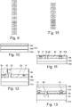
- a method of manufacturing the laser source 10 will now be described with reference to the method of the figure 9 and with the help of Figures 10 to 14 .
- the waveguides 15 and 25 and the reflectors 12 and 14 are made in the silicon layer 66. For example, they are produced by photolithography and etching of this layer 66. In this step, the parts of the couplers 26 and 32 that are in the layer 66 are also produced.
- the layer 66 is encapsulated in a layer 114 ( figure 11 ) of silicon oxide.
- This layer 114 is polished, that is to say planarized, for example, by a physico-chemical polishing process, better known by the acronym CMP ("Chemical Mechanical Planarization"), in order to planarize the upper face of this layer 114.
- CMP Chemical Mechanical Planarization
- a silicon nitride layer is deposited on the upper face of the layer 114.
- this silicon nitride layer is etched to form the waveguide 50 and then encapsulated in silicon.
- the waveguide 50 is shown in the form of a block of silicon nitride.
- the upper face of the layer 64 is then polished, for example, as described with reference to step 112.
- a substrate 122 ( figure 13 ) is bonded to the silicon oxide outer face of the layer 64.
- the substrate 122 is a silicon substrate which comprises a thick layer of silicon oxide at the top. It is these layers of silicon oxide that are glued to one another.
- a step 124 the silicon layer 104 is removed, and the layer 106 is thinned to leave only a thin intermediate layer 126 ( figure 14 ) of silicon oxide.
- the outer face of the layer 126 is polished as described with reference to step 112.
- the layer 68 of III-V gain material is bonded or deposited on the layer 126.
- the layer 68 ( figure 8 ) of III-V gain material is adhered to the outer face of the layer 126.
- the layer 68 comprises the lower sub-layer 70, the stack of alternating sub-layers of GaInNAs and GaNAs and the upper sub-layer doped.
- the layer 68 is etched to produce the waveguide 28, the amplifier 30 and the resistor 80.
- the layer 68 is etched to produce the waveguide 28, the amplifier 30 and the resistor 80.
- upper layers of the layer 68 are etched to structure the amplifier 30.
- the sub-layer 70 is etched to finalize the amplifier structuring 30 and to achieve the resistor 80.
- a step 132 the envelope 90 and the catches 74, 76, 82 and 84 are made.
- the laser source is then obtained, a sectional view of which is shown in FIG. figure 8 .
- the figure 15 represents a second method of manufacturing a laser source 150 ( figure 18 ). This process starts with steps 110 and 112 already described with reference to the method of figure 9 .
- step 152 a layer identical to the previously described layer 68 is glued or deposited on the layer 114 ( figure 16 ). Typically, this layer is bonded by molecular bonding.
- this layer is etched to produce the waveguide 28, the amplifier 30, the resistor 80 and an additional resistor 154 ( figure 16 ). For example, this is done as described with reference to step 128.
- the resistor 154 is used to realize a tuning device 156 ( figure 18 ) for example identical to the tuning device 16, except that it allows to move the reflective strip 4 of the reflector 14 as a function of an electrical control signal generated by the electronic circuit 42.
- This electrical control signal of the device d agreement 156 is typically generated as a function of the measurements of the sensor 40. This makes it possible to reduce, if necessary, the width ⁇ R of the reflecting strip of the reflectors. For example, in this case, it can be as small as N x ⁇ f .
- the resistor 154 is located above the reflector 14.
- the protective envelope 90 is made.
- the waveguide 50 is manufactured in the casing 90 which is made of silicon nitride.
- the waveguide 50 is manufactured by photolithography and etching of the envelope 90 near the ends of the waveguides 15 and 25 ( figure 17 ).
- a step 162 the outlets 74, 76, 82 and 84 are manufactured.
- Contacts 163 and 166 which mechanically and electrically connect the resistor 154 are also fabricated to circulate a current in this resistor 154.
- the combination of the resistor 154 and the receptacles 164 and 166 form the tuning device 156. The result is then the laser source 150 shown on the figure 18 .
- the path of the resonant optical signal in the laser source 150 is represented by a double arrow.
- the laser source 150 is identical to the laser source 10, except that the waveguide 50 and the waveguide 28 are both on the same side of the layer 66. Moreover, in the laser source 150, the reflectors 12 and 14 are turned upward and not downward, as in the laser source 10. This allows to connect the output of the reflector 14 to an optical fiber arriving from above the laser source 150.
- the operation of the laser source 150 is the same as that of the laser source 10, except that the electronic circuit 42 is here also adapted to control the tuning device 156 so as to additionally grant the reflectors 12 and 14.
- the reflectors 182, 184 are identical, respectively, to the reflectors 12 and 14 except that they are made in the same silicon nitride layer as the waveguide 50.
- the reflector 182 is made at one end a silicon nitride waveguide 186 whose other end is optically connected to the waveguide 50 of the ring of the filter 22 by evanescent coupling.
- the waveguide 15 is omitted.
- the waveguide 50 of the ring is optically connected to the waveguide 25 by evanescent coupling as previously described.
- the reflector 184 is formed at the end of a silicon nitride waveguide 188 whose other end is optically connected by adiabatic coupling to the waveguide 25.
- the width ⁇ R of the reflective band of the reflectors 182 and 184 is greater than DT x (d ⁇ Cf / dT).
- the couplers which optically connect the waveguides 25 and 28 to each other are adiabatic couplers.
- the fact of making the reflectors 182 and 184 in a silicon nitride waveguide makes it possible to reduce their bandwidth. This also makes it possible to reduce the interval ⁇ f of the filter 22 to obtain a monochromatic laser source.
- the path of the resonant optical signal is represented by a double arrow.
- the laser source 180 has the advantage that the reflective band 4 of the reflectors 182 and 184 moves much less rapidly than in the laser sources 10 or 150. Indeed, in this embodiment, the variation d ⁇ CR / dT of the length of central wave ⁇ CR is equal to the variation d ⁇ Cf / dT. Thus, whatever the temperature variation, the bandwidth 6 remains always inside the reflective band 4 and does not move with respect to the upper and lower limits of this reflective band 4. The width ⁇ R of the reflective band 4 can then be reduced. Typically, the width ⁇ R is then strictly greater than DT ⁇ d ⁇ Cf / dT + ⁇ f .
- the figure 20 represents a laser source 190 identical to the laser source 180, except that the reflectors 12 and 14 are replaced by reflectors 192 and 194 partly made in the layer 64 and partly in the layer 66.
- the reflectors are made in part silicon nitride and partly silicon.
- each reflector 192 and 194 is formed of two Bragg gratings facing each other, one in the silicon nitride waveguide and one in the silicon waveguide.
- the figure 21 represents a laser source 200 identical to the laser source 150, except that the tuning device 16 is replaced by a tuning device 202.
- the tuning device 202 has a P or N-doped section forming a resistor 204 made in FIG. one of the waveguides 15 or 25. On the figure 21 , the section 204 is formed in the waveguide 15.
- the tuning device 202 also has sockets 206 and 208 for connecting the resistor 204 to the electronic circuit 42. The operation of the laser source 200 is deduced from that of the laser source 150.
- the figure 22 represents a laser source 220 N-wavelengths or polynomatic.
- the laser source 220 is identical to the laser source 10, except that the filter 22 is replaced by a filter 222, and the reflectors 12 and 14 are replaced, respectively, by reflectors 224 and 226.
- the filter 222 is identical to the filter 22, except that the dimensions of the filter 222 are modified so that it has several bandwidths located simultaneously inside the reflecting strip of the reflectors 224 and 226.
- the filter 222 is a resonant ring formed in the waveguide 50 optically connected to the waveguides 15 and 25 by evanescent couplings.
- bandwidths 230 to 232 of the filter 222 are represented as being located inside the reflective band 228 of the reflectors 224 and 226.
- the central wavelengths of these bandwidths are noted, respectively, ⁇ Cf1 , ⁇ Cf2 , and ⁇ Cf3 .
- the symbol ⁇ Cf is used to designate any one of the central wavelengths ⁇ Cf1 , ⁇ Cf2 , and ⁇ Cf3 .
- Each of these bandwidths 230 to 232 is for example identical to the bandwidth 6.
- the interval ⁇ f between two of these successive bandwidths is an integer multiple of the interval ⁇ R and strictly less than the width ⁇ R reflective tape 234.
- the operation of the laser source 220 is identical to that of the laser source 10 except that it simultaneously transmits N wavelengths denoted here ⁇ L1 , ⁇ L2 and ⁇ L3 .
- the Figures 24 and 25 represent a device 236 of agreement likely to advantageously replace the device 16.
- the figure 24 is a vertical sectional view of the device 236 along a transverse sectional plane perpendicular to the waveguide 15.
- the device 236 is able to heat the silicon waveguide 15 as a function of an electrical control signal.
- the device 236 comprises two heaters 237 and 238 symmetrical to one another with respect to a vertical plane 239 ( figure 24 ) passing through the center of the waveguide 15. To simplify the description, only the heater 237 is described in detail.
- the heater 237 comprises, for example, the same elements as the device 16. In particular, it comprises a resistor 240 made in the underlayer 70 and two contact sockets 242A and 242B for circulating a current in the resistor 240. the figure 24 only one 242A socket is visible.
- the heater 237 further comprises a lateral arm 244 made of silicon in the layer 60 is in thermal continuity with the waveguide 15.
- This arm 244 extends in a horizontal transverse direction from the waveguide 15 to the left . Its thickness in the vertical direction is less than that of the waveguide 15. More precisely, its dimensions are such that the optical signal can not propagate inside the arm 244 and remains mainly confined to the interior of an area 245 which surrounds the waveguide 15.
- the arm 244 has a distal portion 246 opposite the resistor 240. the distal portion 246 is separated from the resistor 240 by a thin layer of an SP thickness of silicon oxide.
- the thickness e SP is equal to the thickness of silicon oxide which separates the waveguide 28 from the waveguide 25.
- the distal portion 246 forms a bulge.
- the thickness of the distal portion 246 is equal to the thickness of the waveguide 15.
- the arm 244 forms a single block of material with the waveguide 15.
- the resistor 240 preferentially heats the distal portion 246 and then, by thermal conduction via the arm 244, the heat is transmitted to the waveguide 15.
- the waveguide 15 therefore heats up. turn which varies its refractive index.
- resistor 240 is placed outside zone 245 where the resonant signal flows.
- the resistor 240 is not located, in the vertical direction, above and in relation to the waveguide 15.
- the resistor 80 is vis-à-vis the waveguide 15 and is located inside the zone 245 which causes optical losses .
- the heater 237 does not directly heat the waveguide 15 but heats it mainly through the arm 244 which carries no optical signal.
- the evanescent coupling ratio between the waveguide 262 and the waveguides 264, 266 are the same as those described in the case of the filter 22.
- the two waveguides 264, 266 are optically connected by the intermediate of the adiabatic couplers 268 and 270, respectively, to the waveguides 15 and 25.
- the waveguide 262 is not directly optically connected to the waveguides 15 and 25, but connected to these waveguides via waveguides 264 and 266 made of silicon nitride.
- the tuning device 16 or 156 may be omitted.
- an additional tuning device such as the tuner 156, may be added in any of the previously described embodiments for moving the reflective band of the reflectors.
- the tuning device is not necessarily a heater.
- the refractive index of silicon at level of this PN junction varies depending on the polarization of this junction.
- the electronic control signal of the tuning device then varies the polarization of this PN junction. This way of varying the refractive index of silicon is for example described in more detail in the following article: GT Reed et al., Silicon optical modulators, Natures photonics, Vol 4, August 2010 .
- the reflection factors of the front and back reflectors can also be equal.
- the width ⁇ R of the reflective band of the reflectors 182 and 184 can be reduced. However, it is preferably greater than N x ⁇ f + DT x (d ⁇ Cf / dT), where N is an integer greater than or equal to two and equal to the number of wavelengths ⁇ Rj selected by the filter 222 .
- the waveguide 28 comprises successively, away from the substrate 60: a doped lower sublayer, a quaternary quantum well stack and a doped upper sublayer of opposite sign to the lower sublayer.
- the doped sub-layer 70 may be made of other materials such as N- or P-doped InP.
- the quantum well stack comprises sub-layers of InGaAsP or GaInNAs or others.
- waveguide 28 and amplifier 30 are optically connected to waveguides 15 and 25 by evanescent coupling.
- the adiabatic couplers 26 and 32 are omitted.
- Such an optical connection between the amplifier and silicon waveguides is described, for example, in the following article: AW Fang et al., "Electrically pumped hybrid AlGaInAs-silicon evanescent laser", Optics Express, Vol. 14, pp. 9203-9210 (2006) ).
- the senor 40 is replaced by a sensor of the operating temperature of the laser source. Indeed, at each operating temperature of the laser source, it is possible to associate a difference between the wavelengths ⁇ Cf and ⁇ Rj .
- the electronic circuit 42 comprises a pre-recorded table which associates with several operating temperatures of the laser source, the characteristics of the electrical control signal to be generated to maintain the wavelength ⁇ Li in the center of the the bandwidth 6 of the filter.
- this pre-recorded table is built experimentally.
- the temperature of the laser source can be measured using a transducer, like a PN junction. Indeed, the electrical characteristics of a PN junction varies depending on the temperature.
- the heater 238 is omitted.
- the device 236 is no longer symmetrical with respect to the plane 239.
- the bulge 246 is omitted.
- the filter is coupled to the silicon waveguide by adiabatic couplers such as the adiabatic couplers 268 and 270 shown in FIG. figure 26 and no longer by an evanescent coupling.
- silicon nitride it is also possible to use other materials than silicon nitride.
- silicon nitride it is also possible to use aluminum nitride as a less sensitive material.
- a laser source that emits at several wavelengths ⁇ Li can also be realized as described, for example, with reference to the figures 2 or 6 of the following article: Katarzyna Lawmiczuk et al. Photonics Applications in Astronomy, Communications, Industry and High-Energy Physics Experiments 2010 Proceedings of SPIE, vol 7745, 2010 .
- the filter is a demultiplexer multiplexer known by the acronym AWG ("Array Waveguide Grating"). It is then this AWG component that is made in the material less sensitive to temperature.
- the method described with reference to figure 17 of the following article can easily be adapted to manufacture a laser source such as laser source 150: Martijn JR Heck et al., "Ultra-low loss waveguide platform and its integration with silicon photonics", Laser photonics rev. 8, No. 5, pages 667-686 (2014) ).
- the waveguide 50 is manufactured in a first substrate.
- a second SOI substrate is adhered to the first substrate.
- the waveguides 15 and 25 are then made in the silicon layer of this second substrate.
- the layer 68 is glued over the silicon waveguide and the amplifier 30 is made in this layer 68.
- the intermediate layer 126 is obtained by removing all of the layer 106 and then depositing on the layer 66 exposed a layer of silicon oxide.
- the filter 22 may be placed between the coupler 32 and the reflector 14.
- the tuner 236 may be used in any semiconductor photonic system where it is necessary to heat an optical waveguide by limiting losses. In particular, it can be used to heat a waveguide of another system than a laser source. This other system can be a modulator of phase or intensity of an optical signal.
Landscapes
- Physics & Mathematics (AREA)
- Condensed Matter Physics & Semiconductors (AREA)
- General Physics & Mathematics (AREA)
- Electromagnetism (AREA)
- Optics & Photonics (AREA)
- Geometry (AREA)
- Semiconductor Lasers (AREA)
- Optical Integrated Circuits (AREA)
Applications Claiming Priority (1)
| Application Number | Priority Date | Filing Date | Title |
|---|---|---|---|
| FR1650171A FR3046705B1 (fr) | 2016-01-08 | 2016-01-08 | Source laser a semi-conducteur |
Publications (2)
| Publication Number | Publication Date |
|---|---|
| EP3190672A1 true EP3190672A1 (de) | 2017-07-12 |
| EP3190672B1 EP3190672B1 (de) | 2018-04-18 |
Family
ID=55862946
Family Applications (1)
| Application Number | Title | Priority Date | Filing Date |
|---|---|---|---|
| EP17150156.2A Active EP3190672B1 (de) | 2016-01-08 | 2017-01-03 | Laserquelle mit halbleiter |
Country Status (4)
| Country | Link |
|---|---|
| US (1) | US10270222B2 (de) |
| EP (1) | EP3190672B1 (de) |
| JP (1) | JP6846203B2 (de) |
| FR (1) | FR3046705B1 (de) |
Cited By (4)
| Publication number | Priority date | Publication date | Assignee | Title |
|---|---|---|---|---|
| WO2019002763A1 (fr) | 2017-06-29 | 2019-01-03 | Commissariat à l'énergie atomique et aux énergies alternatives | Source laser à semi-conducteur |
| US20200313389A1 (en) * | 2019-03-27 | 2020-10-01 | Samsung Electronics Co., Ltd. | Laser device and method of transforming laser spectrum |
| WO2022090569A1 (fr) * | 2020-11-02 | 2022-05-05 | Almae Technologies | Systèmes d'émission de lumière non refroidis |
| US20220190922A1 (en) * | 2020-12-16 | 2022-06-16 | Mellanox Technologies, Ltd. | Heterogeneous integration of frequency comb generators for high-speed transceivers |
Families Citing this family (9)
| Publication number | Priority date | Publication date | Assignee | Title |
|---|---|---|---|---|
| FR3074973B1 (fr) | 2017-12-12 | 2019-12-06 | Commissariat A L'energie Atomique Et Aux Energies Alternatives | Emetteur d'un signal optique monochromatique |
| FR3078835B1 (fr) * | 2018-03-12 | 2020-04-17 | Commissariat A L'energie Atomique Et Aux Energies Alternatives | Dispositif photonique comportant un laser optiquement connecte a un guide d'onde silicium et procede de fabrication d'un tel dispositif photonique |
| FR3088776B1 (fr) | 2018-11-15 | 2020-11-20 | Commissariat Energie Atomique | Source laser a semi-conducteur |
| FR3088777B1 (fr) | 2018-11-15 | 2020-11-20 | Commissariat Energie Atomique | Source laser a semi-conducteur et procede d'emission avec cette source laser |
| EP3840138A1 (de) * | 2019-12-17 | 2021-06-23 | FRAUNHOFER-GESELLSCHAFT zur Förderung der angewandten Forschung e.V. | Dwdm-intra-resonator-laservorrichtung |
| FR3109242B1 (fr) | 2020-04-10 | 2022-03-18 | Commissariat Energie Atomique | Procédé de fabrication d’une couche mixte comportant un guide d’onde en silicium et un guide d’onde en nitrure de silicium |
| KR102899215B1 (ko) * | 2020-06-03 | 2025-12-10 | 삼성전자주식회사 | 파장 가변 레이저 광원 및 이를 포함하는 광 조향 장치 |
| FR3121783B1 (fr) * | 2021-04-07 | 2023-11-10 | Scintil Photonics | Procéde de fabrication d’un dispositif photonique pourvu d’au moins deux puces photoniques et dispositif photonique |
| US12345921B2 (en) * | 2022-11-08 | 2025-07-01 | SiFotonics Technologies (Beijing) Co., Ltd. | Silicon-based integrated optical chip |
Citations (6)
| Publication number | Priority date | Publication date | Assignee | Title |
|---|---|---|---|---|
| US20090135861A1 (en) * | 2007-11-09 | 2009-05-28 | Lightwire, Inc. | Soi-based tunable laser |
| US20090135891A1 (en) | 2005-07-26 | 2009-05-28 | Advantest Corporation | Symbol modulation accuracy measuring device, method, program, and recording medium |
| US20140153600A1 (en) | 2012-11-29 | 2014-06-05 | Agency For Science, Technology And Research | Optical Light Source |
| US20140153601A1 (en) | 2012-04-26 | 2014-06-05 | Acacia Communications Inc. | Tunable laser using iii-v gain materials |
| US20150180201A1 (en) | 2013-11-20 | 2015-06-25 | Coriant Advanced Technology, LLC | Quantum dot soa-silicon external cavity multi-wavelength laser |
| GB2522252A (en) | 2014-01-20 | 2015-07-22 | Rockley Photonics Ltd | Tunable SOI laser |
Family Cites Families (6)
| Publication number | Priority date | Publication date | Assignee | Title |
|---|---|---|---|---|
| US6856641B2 (en) * | 2001-01-26 | 2005-02-15 | California Institute Of Technology | Ring resonator based narrow-linewidth semiconductor lasers |
| JP2009278015A (ja) * | 2008-05-16 | 2009-11-26 | Nec Corp | 平面光波回路及びこれを備えた波長可変レーザ装置 |
| JP5764875B2 (ja) * | 2010-06-02 | 2015-08-19 | 富士通株式会社 | 半導体光装置 |
| JP5728964B2 (ja) * | 2011-01-20 | 2015-06-03 | 富士通株式会社 | 光半導体装置及びその製造方法 |
| FR3007589B1 (fr) | 2013-06-24 | 2015-07-24 | St Microelectronics Crolles 2 | Circuit integre photonique et procede de fabrication |
| US9837781B2 (en) * | 2014-10-24 | 2017-12-05 | Oracle International Corporation | External cavity laser with reduced optical mode-hopping |
-
2016
- 2016-01-08 FR FR1650171A patent/FR3046705B1/fr not_active Expired - Fee Related
-
2017
- 2017-01-03 EP EP17150156.2A patent/EP3190672B1/de active Active
- 2017-01-05 US US15/399,312 patent/US10270222B2/en active Active
- 2017-01-06 JP JP2017000852A patent/JP6846203B2/ja active Active
Patent Citations (6)
| Publication number | Priority date | Publication date | Assignee | Title |
|---|---|---|---|---|
| US20090135891A1 (en) | 2005-07-26 | 2009-05-28 | Advantest Corporation | Symbol modulation accuracy measuring device, method, program, and recording medium |
| US20090135861A1 (en) * | 2007-11-09 | 2009-05-28 | Lightwire, Inc. | Soi-based tunable laser |
| US20140153601A1 (en) | 2012-04-26 | 2014-06-05 | Acacia Communications Inc. | Tunable laser using iii-v gain materials |
| US20140153600A1 (en) | 2012-11-29 | 2014-06-05 | Agency For Science, Technology And Research | Optical Light Source |
| US20150180201A1 (en) | 2013-11-20 | 2015-06-25 | Coriant Advanced Technology, LLC | Quantum dot soa-silicon external cavity multi-wavelength laser |
| GB2522252A (en) | 2014-01-20 | 2015-07-22 | Rockley Photonics Ltd | Tunable SOI laser |
Non-Patent Citations (10)
| Title |
|---|
| A. W. FANG ET AL.: "Electrically pumped hybrid AIGalnAs-silicon evanescent laser", OPTICS EXPRESS, vol. 14, 2006, pages 9203 - 9210 |
| AMNON YARIV ET AL.: "Supermode Si/lll-V hybrid Lasers, optical amplifiers and modulators: proposai and analysis", OPTICS EXPRESS 9147, vol. 14, no. 15, 23 July 2007 (2007-07-23) |
| B. BEN BAKIR ET AL., HYBRID SI/LLL-V LASERS WITH ADIABATIC COUPLING, 2011 |
| DIMITRIS FITSIOS ET AL.: "High-gain 1,3 pm GalnNAs semiconductor optical amplifier with enchanced temperature stability for all-optical processing at 10 Gb/s", APPLIED OPTICS, vol. 54, no. L, 1 January 2015 (2015-01-01) |
| G.T. REED ET AL.: "Silicon optical modulators", NATURES PHOTONICS, vol. 4, August 2010 (2010-08-01) |
| K. MORITO ET AL.: "ECOC", 2006, IEEE, article "GainNAs / InP Tensile-Strained Bulk Polarization-Insensitive SOA" |
| KATARZYNA LAWMICZUK ET AL.: "Design of integrated photonic transmitter for application in fiber-to-the-home systems", PHOTONICS APPLICATIONS IN ASTRONOMY, COMMUNICATIONS, INDUSTRY AND HIGH-ENERGY PHYSICS EXPERIMENTS 2010 PROCEEDINGS OF SPIE, vol. 7745, 2010 |
| MARTIJN J.R. HECK ET AL.: "Ultra-low loss waveguide plateform and its intégration with silicon photonics", LASER PHOTONICS REV., vol. 8, no. 5, 2014, pages 667 - 686 |
| NOBUHIDE FUJIOKA ET AL: "Compact and Low Power Consumption Hybrid Integrated Wavelength Tunable Laser Module Using Silicon Waveguide Resonators", JOURNAL OF LIGHTWAVE TECHNOLOGY, IEEE SERVICE CENTER, NEW YORK, NY, US, vol. 28, no. 21, 1 November 2010 (2010-11-01), pages 3115 - 3120, XP011339909, ISSN: 0733-8724, DOI: 10.1109/JLT.2010.2073445 * |
| NOBUHIDE FUJIOKA: "Journal of Lightwave Technology", vol. 28, IEEE SERVICE CENTER, article "Compact and Low Power Consumption Hybrid Integrated Wavelength Tunable Laser Module Using Silicon Waveguide Resonators" |
Cited By (8)
| Publication number | Priority date | Publication date | Assignee | Title |
|---|---|---|---|---|
| WO2019002763A1 (fr) | 2017-06-29 | 2019-01-03 | Commissariat à l'énergie atomique et aux énergies alternatives | Source laser à semi-conducteur |
| FR3068527A1 (fr) * | 2017-06-29 | 2019-01-04 | Commissariat A L'energie Atomique Et Aux Energies Alternatives | Source laser a semi-conducteur |
| US20200313389A1 (en) * | 2019-03-27 | 2020-10-01 | Samsung Electronics Co., Ltd. | Laser device and method of transforming laser spectrum |
| US11804694B2 (en) * | 2019-03-27 | 2023-10-31 | Samsung Electronics Co., Ltd. | Laser device and method of transforming laser spectrum |
| WO2022090569A1 (fr) * | 2020-11-02 | 2022-05-05 | Almae Technologies | Systèmes d'émission de lumière non refroidis |
| FR3115893A1 (fr) * | 2020-11-02 | 2022-05-06 | Almae Technologies | Systèmes d’émission de lumière non refroidi |
| US20220190922A1 (en) * | 2020-12-16 | 2022-06-16 | Mellanox Technologies, Ltd. | Heterogeneous integration of frequency comb generators for high-speed transceivers |
| US11791902B2 (en) * | 2020-12-16 | 2023-10-17 | Mellanox Technologies, Ltd. | Heterogeneous integration of frequency comb generators for high-speed transceivers |
Also Published As
| Publication number | Publication date |
|---|---|
| JP6846203B2 (ja) | 2021-03-24 |
| EP3190672B1 (de) | 2018-04-18 |
| US20180261976A1 (en) | 2018-09-13 |
| FR3046705B1 (fr) | 2018-02-16 |
| FR3046705A1 (fr) | 2017-07-14 |
| JP2017152683A (ja) | 2017-08-31 |
| US10270222B2 (en) | 2019-04-23 |
Similar Documents
| Publication | Publication Date | Title |
|---|---|---|
| EP3190672B1 (de) | Laserquelle mit halbleiter | |
| EP3385784B1 (de) | Optoelektronische vorrichtung zur erzeugung eines frequenzkamms | |
| EP3540878B1 (de) | Photonenvorrichtung, die einen laser umfasst, der optisch mit einem silizium-wellenleiter verbunden ist, und herstellungsverfahren einer solchen photonenvorrichtung | |
| EP1364190B1 (de) | Optoelektronische vorrichtung zur wellenlängenfilterung durch kavitätenkopplung | |
| EP3206079B1 (de) | Photonischer sender | |
| EP0033048B1 (de) | Interferometer mit abstimmbarer optischer Höhlung, das eine optische monomoden Faser befasst, und dessen Anwendung zur Filtrierung und Spektrographie | |
| EP1909080A1 (de) | Ultrasensibler optischer Detektor mit hoher zeitlicher Auflösung basierend auf einem Gitter. | |
| WO2019002763A1 (fr) | Source laser à semi-conducteur | |
| EP4133317B1 (de) | Verfahren zur herstellung einer mischschicht mit einem siliziumwellenleiter und einem siliziumnitridwellenleiter | |
| WO2010109134A1 (fr) | Modulateur optique a haut debit en semi-conducteur sur isolant. | |
| EP3264541B1 (de) | Laserquelle mit halbleiter | |
| FR2821495A1 (fr) | Laser accordable de facon rapide et large | |
| EP1929539B1 (de) | Einen planarwellenleiter-leckmodus verwendender zeitlich hoch auflösender ultraempfindlicher optischer sensor und herstellungsverfahren dafür | |
| EP3654463B1 (de) | Laserquelle mit halbleiter | |
| EP3654462B1 (de) | Laserquelle mit halbleiter und emissionsverfahren mit dieser laserquelle | |
| FR3071676B1 (fr) | Source laser a membrane suspendue a base de germanium et guide d'onde integre participant a former la cavite optique | |
| FR2857159A1 (fr) | Photodetecteur a cavite verticale resonnante, matrice et systeme de telecommunication correspondant. | |
| FR3052562B1 (fr) | Dispositif optique | |
| EP1306941A1 (de) | Optische Resonator in Resonanz in einem kontinuerlichen Frequenzbereich | |
| FR3065323B1 (fr) | Photodiode | |
| WO2002013335A2 (fr) | Laser accordable en semi-conducteur a emission par la tranche | |
| FR3080924A1 (fr) | Dispositif electro-optique integre | |
| EP3599501B1 (de) | Athermischer modulator-umschalter mit zwei übereinander angeordneten ringen | |
| EP4557537A1 (de) | Integrierte hochleistungslaseremissionsvorrichtung |
Legal Events
| Date | Code | Title | Description |
|---|---|---|---|
| PUAI | Public reference made under article 153(3) epc to a published international application that has entered the european phase |
Free format text: ORIGINAL CODE: 0009012 |
|
| STAA | Information on the status of an ep patent application or granted ep patent |
Free format text: STATUS: REQUEST FOR EXAMINATION WAS MADE |
|
| 17P | Request for examination filed |
Effective date: 20170103 |
|
| AK | Designated contracting states |
Kind code of ref document: A1 Designated state(s): AL AT BE BG CH CY CZ DE DK EE ES FI FR GB GR HR HU IE IS IT LI LT LU LV MC MK MT NL NO PL PT RO RS SE SI SK SM TR |
|
| AX | Request for extension of the european patent |
Extension state: BA ME |
|
| GRAP | Despatch of communication of intention to grant a patent |
Free format text: ORIGINAL CODE: EPIDOSNIGR1 |
|
| STAA | Information on the status of an ep patent application or granted ep patent |
Free format text: STATUS: GRANT OF PATENT IS INTENDED |
|
| INTG | Intention to grant announced |
Effective date: 20171002 |
|
| GRAS | Grant fee paid |
Free format text: ORIGINAL CODE: EPIDOSNIGR3 |
|
| GRAA | (expected) grant |
Free format text: ORIGINAL CODE: 0009210 |
|
| STAA | Information on the status of an ep patent application or granted ep patent |
Free format text: STATUS: THE PATENT HAS BEEN GRANTED |
|
| AK | Designated contracting states |
Kind code of ref document: B1 Designated state(s): AL AT BE BG CH CY CZ DE DK EE ES FI FR GB GR HR HU IE IS IT LI LT LU LV MC MK MT NL NO PL PT RO RS SE SI SK SM TR |
|
| REG | Reference to a national code |
Ref country code: GB Ref legal event code: FG4D Free format text: NOT ENGLISH |
|
| REG | Reference to a national code |
Ref country code: CH Ref legal event code: EP |
|
| REG | Reference to a national code |
Ref country code: DE Ref legal event code: R096 Ref document number: 602017000033 Country of ref document: DE |
|
| REG | Reference to a national code |
Ref country code: AT Ref legal event code: REF Ref document number: 991436 Country of ref document: AT Kind code of ref document: T Effective date: 20180515 |
|
| REG | Reference to a national code |
Ref country code: IE Ref legal event code: FG4D Free format text: LANGUAGE OF EP DOCUMENT: FRENCH |
|
| REG | Reference to a national code |
Ref country code: NL Ref legal event code: MP Effective date: 20180418 |
|
| REG | Reference to a national code |
Ref country code: LT Ref legal event code: MG4D |
|
| PG25 | Lapsed in a contracting state [announced via postgrant information from national office to epo] |
Ref country code: NL Free format text: LAPSE BECAUSE OF FAILURE TO SUBMIT A TRANSLATION OF THE DESCRIPTION OR TO PAY THE FEE WITHIN THE PRESCRIBED TIME-LIMIT Effective date: 20180418 |
|
| PG25 | Lapsed in a contracting state [announced via postgrant information from national office to epo] |
Ref country code: BG Free format text: LAPSE BECAUSE OF FAILURE TO SUBMIT A TRANSLATION OF THE DESCRIPTION OR TO PAY THE FEE WITHIN THE PRESCRIBED TIME-LIMIT Effective date: 20180718 Ref country code: SE Free format text: LAPSE BECAUSE OF FAILURE TO SUBMIT A TRANSLATION OF THE DESCRIPTION OR TO PAY THE FEE WITHIN THE PRESCRIBED TIME-LIMIT Effective date: 20180418 Ref country code: ES Free format text: LAPSE BECAUSE OF FAILURE TO SUBMIT A TRANSLATION OF THE DESCRIPTION OR TO PAY THE FEE WITHIN THE PRESCRIBED TIME-LIMIT Effective date: 20180418 Ref country code: NO Free format text: LAPSE BECAUSE OF FAILURE TO SUBMIT A TRANSLATION OF THE DESCRIPTION OR TO PAY THE FEE WITHIN THE PRESCRIBED TIME-LIMIT Effective date: 20180718 Ref country code: PL Free format text: LAPSE BECAUSE OF FAILURE TO SUBMIT A TRANSLATION OF THE DESCRIPTION OR TO PAY THE FEE WITHIN THE PRESCRIBED TIME-LIMIT Effective date: 20180418 Ref country code: LT Free format text: LAPSE BECAUSE OF FAILURE TO SUBMIT A TRANSLATION OF THE DESCRIPTION OR TO PAY THE FEE WITHIN THE PRESCRIBED TIME-LIMIT Effective date: 20180418 Ref country code: AL Free format text: LAPSE BECAUSE OF FAILURE TO SUBMIT A TRANSLATION OF THE DESCRIPTION OR TO PAY THE FEE WITHIN THE PRESCRIBED TIME-LIMIT Effective date: 20180418 Ref country code: FI Free format text: LAPSE BECAUSE OF FAILURE TO SUBMIT A TRANSLATION OF THE DESCRIPTION OR TO PAY THE FEE WITHIN THE PRESCRIBED TIME-LIMIT Effective date: 20180418 |
|
| PG25 | Lapsed in a contracting state [announced via postgrant information from national office to epo] |
Ref country code: LV Free format text: LAPSE BECAUSE OF FAILURE TO SUBMIT A TRANSLATION OF THE DESCRIPTION OR TO PAY THE FEE WITHIN THE PRESCRIBED TIME-LIMIT Effective date: 20180418 Ref country code: HR Free format text: LAPSE BECAUSE OF FAILURE TO SUBMIT A TRANSLATION OF THE DESCRIPTION OR TO PAY THE FEE WITHIN THE PRESCRIBED TIME-LIMIT Effective date: 20180418 Ref country code: GR Free format text: LAPSE BECAUSE OF FAILURE TO SUBMIT A TRANSLATION OF THE DESCRIPTION OR TO PAY THE FEE WITHIN THE PRESCRIBED TIME-LIMIT Effective date: 20180719 Ref country code: RS Free format text: LAPSE BECAUSE OF FAILURE TO SUBMIT A TRANSLATION OF THE DESCRIPTION OR TO PAY THE FEE WITHIN THE PRESCRIBED TIME-LIMIT Effective date: 20180418 |
|
| REG | Reference to a national code |
Ref country code: AT Ref legal event code: MK05 Ref document number: 991436 Country of ref document: AT Kind code of ref document: T Effective date: 20180418 |
|
| REG | Reference to a national code |
Ref country code: DE Ref legal event code: R097 Ref document number: 602017000033 Country of ref document: DE |
|
| PG25 | Lapsed in a contracting state [announced via postgrant information from national office to epo] |
Ref country code: EE Free format text: LAPSE BECAUSE OF FAILURE TO SUBMIT A TRANSLATION OF THE DESCRIPTION OR TO PAY THE FEE WITHIN THE PRESCRIBED TIME-LIMIT Effective date: 20180418 Ref country code: DK Free format text: LAPSE BECAUSE OF FAILURE TO SUBMIT A TRANSLATION OF THE DESCRIPTION OR TO PAY THE FEE WITHIN THE PRESCRIBED TIME-LIMIT Effective date: 20180418 Ref country code: RO Free format text: LAPSE BECAUSE OF FAILURE TO SUBMIT A TRANSLATION OF THE DESCRIPTION OR TO PAY THE FEE WITHIN THE PRESCRIBED TIME-LIMIT Effective date: 20180418 Ref country code: AT Free format text: LAPSE BECAUSE OF FAILURE TO SUBMIT A TRANSLATION OF THE DESCRIPTION OR TO PAY THE FEE WITHIN THE PRESCRIBED TIME-LIMIT Effective date: 20180418 Ref country code: CZ Free format text: LAPSE BECAUSE OF FAILURE TO SUBMIT A TRANSLATION OF THE DESCRIPTION OR TO PAY THE FEE WITHIN THE PRESCRIBED TIME-LIMIT Effective date: 20180418 Ref country code: SK Free format text: LAPSE BECAUSE OF FAILURE TO SUBMIT A TRANSLATION OF THE DESCRIPTION OR TO PAY THE FEE WITHIN THE PRESCRIBED TIME-LIMIT Effective date: 20180418 |
|
| PLBE | No opposition filed within time limit |
Free format text: ORIGINAL CODE: 0009261 |
|
| STAA | Information on the status of an ep patent application or granted ep patent |
Free format text: STATUS: NO OPPOSITION FILED WITHIN TIME LIMIT |
|
| PG25 | Lapsed in a contracting state [announced via postgrant information from national office to epo] |
Ref country code: SM Free format text: LAPSE BECAUSE OF FAILURE TO SUBMIT A TRANSLATION OF THE DESCRIPTION OR TO PAY THE FEE WITHIN THE PRESCRIBED TIME-LIMIT Effective date: 20180418 Ref country code: IT Free format text: LAPSE BECAUSE OF FAILURE TO SUBMIT A TRANSLATION OF THE DESCRIPTION OR TO PAY THE FEE WITHIN THE PRESCRIBED TIME-LIMIT Effective date: 20180418 |
|
| 26N | No opposition filed |
Effective date: 20190121 |
|
| PG25 | Lapsed in a contracting state [announced via postgrant information from national office to epo] |
Ref country code: MC Free format text: LAPSE BECAUSE OF FAILURE TO SUBMIT A TRANSLATION OF THE DESCRIPTION OR TO PAY THE FEE WITHIN THE PRESCRIBED TIME-LIMIT Effective date: 20180418 |
|
| PG25 | Lapsed in a contracting state [announced via postgrant information from national office to epo] |
Ref country code: LU Free format text: LAPSE BECAUSE OF NON-PAYMENT OF DUE FEES Effective date: 20190103 |
|
| REG | Reference to a national code |
Ref country code: BE Ref legal event code: MM Effective date: 20190131 |
|
| REG | Reference to a national code |
Ref country code: IE Ref legal event code: MM4A |
|
| PG25 | Lapsed in a contracting state [announced via postgrant information from national office to epo] |
Ref country code: BE Free format text: LAPSE BECAUSE OF NON-PAYMENT OF DUE FEES Effective date: 20190131 |
|
| PG25 | Lapsed in a contracting state [announced via postgrant information from national office to epo] |
Ref country code: IE Free format text: LAPSE BECAUSE OF NON-PAYMENT OF DUE FEES Effective date: 20190103 |
|
| PG25 | Lapsed in a contracting state [announced via postgrant information from national office to epo] |
Ref country code: TR Free format text: LAPSE BECAUSE OF FAILURE TO SUBMIT A TRANSLATION OF THE DESCRIPTION OR TO PAY THE FEE WITHIN THE PRESCRIBED TIME-LIMIT Effective date: 20180418 |
|
| PG25 | Lapsed in a contracting state [announced via postgrant information from national office to epo] |
Ref country code: PT Free format text: LAPSE BECAUSE OF FAILURE TO SUBMIT A TRANSLATION OF THE DESCRIPTION OR TO PAY THE FEE WITHIN THE PRESCRIBED TIME-LIMIT Effective date: 20180820 Ref country code: MT Free format text: LAPSE BECAUSE OF FAILURE TO SUBMIT A TRANSLATION OF THE DESCRIPTION OR TO PAY THE FEE WITHIN THE PRESCRIBED TIME-LIMIT Effective date: 20180418 |
|
| REG | Reference to a national code |
Ref country code: CH Ref legal event code: PL |
|
| PG25 | Lapsed in a contracting state [announced via postgrant information from national office to epo] |
Ref country code: CH Free format text: LAPSE BECAUSE OF NON-PAYMENT OF DUE FEES Effective date: 20200131 Ref country code: LI Free format text: LAPSE BECAUSE OF NON-PAYMENT OF DUE FEES Effective date: 20200131 |
|
| PG25 | Lapsed in a contracting state [announced via postgrant information from national office to epo] |
Ref country code: CY Free format text: LAPSE BECAUSE OF FAILURE TO SUBMIT A TRANSLATION OF THE DESCRIPTION OR TO PAY THE FEE WITHIN THE PRESCRIBED TIME-LIMIT Effective date: 20180418 |
|
| PG25 | Lapsed in a contracting state [announced via postgrant information from national office to epo] |
Ref country code: IS Free format text: LAPSE BECAUSE OF FAILURE TO SUBMIT A TRANSLATION OF THE DESCRIPTION OR TO PAY THE FEE WITHIN THE PRESCRIBED TIME-LIMIT Effective date: 20180818 |
|
| PG25 | Lapsed in a contracting state [announced via postgrant information from national office to epo] |
Ref country code: HU Free format text: LAPSE BECAUSE OF FAILURE TO SUBMIT A TRANSLATION OF THE DESCRIPTION OR TO PAY THE FEE WITHIN THE PRESCRIBED TIME-LIMIT; INVALID AB INITIO Effective date: 20170103 |
|
| PG25 | Lapsed in a contracting state [announced via postgrant information from national office to epo] |
Ref country code: SI Free format text: LAPSE BECAUSE OF FAILURE TO SUBMIT A TRANSLATION OF THE DESCRIPTION OR TO PAY THE FEE WITHIN THE PRESCRIBED TIME-LIMIT Effective date: 20180418 |
|
| PG25 | Lapsed in a contracting state [announced via postgrant information from national office to epo] |
Ref country code: MK Free format text: LAPSE BECAUSE OF FAILURE TO SUBMIT A TRANSLATION OF THE DESCRIPTION OR TO PAY THE FEE WITHIN THE PRESCRIBED TIME-LIMIT Effective date: 20180418 |
|
| P01 | Opt-out of the competence of the unified patent court (upc) registered |
Effective date: 20230517 |
|
| PGFP | Annual fee paid to national office [announced via postgrant information from national office to epo] |
Ref country code: GB Payment date: 20260121 Year of fee payment: 10 |
|
| PGFP | Annual fee paid to national office [announced via postgrant information from national office to epo] |
Ref country code: DE Payment date: 20260120 Year of fee payment: 10 |
|
| PGFP | Annual fee paid to national office [announced via postgrant information from national office to epo] |
Ref country code: FR Payment date: 20260128 Year of fee payment: 10 |