EP3203280A1 - Substrat zur farbumwandlung, herstellungsverfahren dafür und anzeigevorrichtung damit - Google Patents
Substrat zur farbumwandlung, herstellungsverfahren dafür und anzeigevorrichtung damit Download PDFInfo
- Publication number
- EP3203280A1 EP3203280A1 EP15848034.3A EP15848034A EP3203280A1 EP 3203280 A1 EP3203280 A1 EP 3203280A1 EP 15848034 A EP15848034 A EP 15848034A EP 3203280 A1 EP3203280 A1 EP 3203280A1
- Authority
- EP
- European Patent Office
- Prior art keywords
- thin glass
- glass plate
- light guide
- coating layer
- color conversion
- Prior art date
- Legal status (The legal status is an assumption and is not a legal conclusion. Google has not performed a legal analysis and makes no representation as to the accuracy of the status listed.)
- Withdrawn
Links
Images
Classifications
-
- F—MECHANICAL ENGINEERING; LIGHTING; HEATING; WEAPONS; BLASTING
- F21—LIGHTING
- F21V—FUNCTIONAL FEATURES OR DETAILS OF LIGHTING DEVICES OR SYSTEMS THEREOF; STRUCTURAL COMBINATIONS OF LIGHTING DEVICES WITH OTHER ARTICLES, NOT OTHERWISE PROVIDED FOR
- F21V9/00—Elements for modifying spectral properties, polarisation or intensity of the light emitted, e.g. filters
- F21V9/30—Elements containing photoluminescent material distinct from or spaced from the light source
- F21V9/32—Elements containing photoluminescent material distinct from or spaced from the light source characterised by the arrangement of the photoluminescent material
-
- G—PHYSICS
- G02—OPTICS
- G02B—OPTICAL ELEMENTS, SYSTEMS OR APPARATUS
- G02B6/00—Light guides; Structural details of arrangements comprising light guides and other optical elements, e.g. couplings
- G02B6/02—Optical fibres with cladding with or without a coating
- G02B6/0229—Optical fibres with cladding with or without a coating characterised by nanostructures, i.e. structures of size less than 100 nm, e.g. quantum dots
-
- G—PHYSICS
- G02—OPTICS
- G02F—OPTICAL DEVICES OR ARRANGEMENTS FOR THE CONTROL OF LIGHT BY MODIFICATION OF THE OPTICAL PROPERTIES OF THE MEDIA OF THE ELEMENTS INVOLVED THEREIN; NON-LINEAR OPTICS; FREQUENCY-CHANGING OF LIGHT; OPTICAL LOGIC ELEMENTS; OPTICAL ANALOGUE/DIGITAL CONVERTERS
- G02F1/00—Devices or arrangements for the control of the intensity, colour, phase, polarisation or direction of light arriving from an independent light source, e.g. switching, gating or modulating; Non-linear optics
- G02F1/01—Devices or arrangements for the control of the intensity, colour, phase, polarisation or direction of light arriving from an independent light source, e.g. switching, gating or modulating; Non-linear optics for the control of the intensity, phase, polarisation or colour
- G02F1/13—Devices or arrangements for the control of the intensity, colour, phase, polarisation or direction of light arriving from an independent light source, e.g. switching, gating or modulating; Non-linear optics for the control of the intensity, phase, polarisation or colour based on liquid crystals, e.g. single liquid crystal display cells
- G02F1/133—Constructional arrangements; Operation of liquid crystal cells; Circuit arrangements
- G02F1/1333—Constructional arrangements; Manufacturing methods
- G02F1/1335—Structural association of cells with optical devices, e.g. polarisers or reflectors
- G02F1/1336—Illuminating devices
- G02F1/133615—Edge-illuminating devices, i.e. illuminating from the side
-
- F—MECHANICAL ENGINEERING; LIGHTING; HEATING; WEAPONS; BLASTING
- F21—LIGHTING
- F21V—FUNCTIONAL FEATURES OR DETAILS OF LIGHTING DEVICES OR SYSTEMS THEREOF; STRUCTURAL COMBINATIONS OF LIGHTING DEVICES WITH OTHER ARTICLES, NOT OTHERWISE PROVIDED FOR
- F21V9/00—Elements for modifying spectral properties, polarisation or intensity of the light emitted, e.g. filters
- F21V9/30—Elements containing photoluminescent material distinct from or spaced from the light source
-
- F—MECHANICAL ENGINEERING; LIGHTING; HEATING; WEAPONS; BLASTING
- F21—LIGHTING
- F21V—FUNCTIONAL FEATURES OR DETAILS OF LIGHTING DEVICES OR SYSTEMS THEREOF; STRUCTURAL COMBINATIONS OF LIGHTING DEVICES WITH OTHER ARTICLES, NOT OTHERWISE PROVIDED FOR
- F21V9/00—Elements for modifying spectral properties, polarisation or intensity of the light emitted, e.g. filters
- F21V9/40—Elements for modifying spectral properties, polarisation or intensity of the light emitted, e.g. filters with provision for controlling spectral properties, e.g. colour, or intensity
- F21V9/45—Elements for modifying spectral properties, polarisation or intensity of the light emitted, e.g. filters with provision for controlling spectral properties, e.g. colour, or intensity by adjustment of photoluminescent elements
-
- G—PHYSICS
- G02—OPTICS
- G02B—OPTICAL ELEMENTS, SYSTEMS OR APPARATUS
- G02B6/00—Light guides; Structural details of arrangements comprising light guides and other optical elements, e.g. couplings
- G02B6/0001—Light guides; Structural details of arrangements comprising light guides and other optical elements, e.g. couplings specially adapted for lighting devices or systems
- G02B6/0011—Light guides; Structural details of arrangements comprising light guides and other optical elements, e.g. couplings specially adapted for lighting devices or systems the light guides being planar or of plate-like form
- G02B6/0033—Means for improving the coupling-out of light from the light guide
- G02B6/005—Means for improving the coupling-out of light from the light guide provided by one optical element, or plurality thereof, placed on the light output side of the light guide
-
- G—PHYSICS
- G02—OPTICS
- G02B—OPTICAL ELEMENTS, SYSTEMS OR APPARATUS
- G02B6/00—Light guides; Structural details of arrangements comprising light guides and other optical elements, e.g. couplings
- G02B6/0001—Light guides; Structural details of arrangements comprising light guides and other optical elements, e.g. couplings specially adapted for lighting devices or systems
- G02B6/0011—Light guides; Structural details of arrangements comprising light guides and other optical elements, e.g. couplings specially adapted for lighting devices or systems the light guides being planar or of plate-like form
- G02B6/0066—Light guides; Structural details of arrangements comprising light guides and other optical elements, e.g. couplings specially adapted for lighting devices or systems the light guides being planar or of plate-like form characterised by the light source being coupled to the light guide
- G02B6/0073—Light emitting diode [LED]
-
- G—PHYSICS
- G02—OPTICS
- G02B—OPTICAL ELEMENTS, SYSTEMS OR APPARATUS
- G02B6/00—Light guides; Structural details of arrangements comprising light guides and other optical elements, e.g. couplings
- G02B6/0001—Light guides; Structural details of arrangements comprising light guides and other optical elements, e.g. couplings specially adapted for lighting devices or systems
- G02B6/0011—Light guides; Structural details of arrangements comprising light guides and other optical elements, e.g. couplings specially adapted for lighting devices or systems the light guides being planar or of plate-like form
- G02B6/0081—Mechanical or electrical aspects of the light guide and light source in the lighting device peculiar to the adaptation to planar light guides, e.g. concerning packaging
- G02B6/0093—Means for protecting the light guide
-
- G—PHYSICS
- G02—OPTICS
- G02B—OPTICAL ELEMENTS, SYSTEMS OR APPARATUS
- G02B6/00—Light guides; Structural details of arrangements comprising light guides and other optical elements, e.g. couplings
- G02B6/10—Light guides; Structural details of arrangements comprising light guides and other optical elements, e.g. couplings of the optical waveguide type
-
- G—PHYSICS
- G02—OPTICS
- G02F—OPTICAL DEVICES OR ARRANGEMENTS FOR THE CONTROL OF LIGHT BY MODIFICATION OF THE OPTICAL PROPERTIES OF THE MEDIA OF THE ELEMENTS INVOLVED THEREIN; NON-LINEAR OPTICS; FREQUENCY-CHANGING OF LIGHT; OPTICAL LOGIC ELEMENTS; OPTICAL ANALOGUE/DIGITAL CONVERTERS
- G02F1/00—Devices or arrangements for the control of the intensity, colour, phase, polarisation or direction of light arriving from an independent light source, e.g. switching, gating or modulating; Non-linear optics
- G02F1/01—Devices or arrangements for the control of the intensity, colour, phase, polarisation or direction of light arriving from an independent light source, e.g. switching, gating or modulating; Non-linear optics for the control of the intensity, phase, polarisation or colour
- G02F1/13—Devices or arrangements for the control of the intensity, colour, phase, polarisation or direction of light arriving from an independent light source, e.g. switching, gating or modulating; Non-linear optics for the control of the intensity, phase, polarisation or colour based on liquid crystals, e.g. single liquid crystal display cells
- G02F1/133—Constructional arrangements; Operation of liquid crystal cells; Circuit arrangements
- G02F1/1333—Constructional arrangements; Manufacturing methods
- G02F1/1335—Structural association of cells with optical devices, e.g. polarisers or reflectors
- G02F1/1336—Illuminating devices
- G02F1/133602—Direct backlight
- G02F1/133603—Direct backlight with LEDs
-
- G—PHYSICS
- G02—OPTICS
- G02F—OPTICAL DEVICES OR ARRANGEMENTS FOR THE CONTROL OF LIGHT BY MODIFICATION OF THE OPTICAL PROPERTIES OF THE MEDIA OF THE ELEMENTS INVOLVED THEREIN; NON-LINEAR OPTICS; FREQUENCY-CHANGING OF LIGHT; OPTICAL LOGIC ELEMENTS; OPTICAL ANALOGUE/DIGITAL CONVERTERS
- G02F1/00—Devices or arrangements for the control of the intensity, colour, phase, polarisation or direction of light arriving from an independent light source, e.g. switching, gating or modulating; Non-linear optics
- G02F1/01—Devices or arrangements for the control of the intensity, colour, phase, polarisation or direction of light arriving from an independent light source, e.g. switching, gating or modulating; Non-linear optics for the control of the intensity, phase, polarisation or colour
- G02F1/13—Devices or arrangements for the control of the intensity, colour, phase, polarisation or direction of light arriving from an independent light source, e.g. switching, gating or modulating; Non-linear optics for the control of the intensity, phase, polarisation or colour based on liquid crystals, e.g. single liquid crystal display cells
- G02F1/133—Constructional arrangements; Operation of liquid crystal cells; Circuit arrangements
- G02F1/1333—Constructional arrangements; Manufacturing methods
- G02F1/1335—Structural association of cells with optical devices, e.g. polarisers or reflectors
- G02F1/1336—Illuminating devices
- G02F1/133621—Illuminating devices providing coloured light
-
- G—PHYSICS
- G02—OPTICS
- G02F—OPTICAL DEVICES OR ARRANGEMENTS FOR THE CONTROL OF LIGHT BY MODIFICATION OF THE OPTICAL PROPERTIES OF THE MEDIA OF THE ELEMENTS INVOLVED THEREIN; NON-LINEAR OPTICS; FREQUENCY-CHANGING OF LIGHT; OPTICAL LOGIC ELEMENTS; OPTICAL ANALOGUE/DIGITAL CONVERTERS
- G02F1/00—Devices or arrangements for the control of the intensity, colour, phase, polarisation or direction of light arriving from an independent light source, e.g. switching, gating or modulating; Non-linear optics
- G02F1/01—Devices or arrangements for the control of the intensity, colour, phase, polarisation or direction of light arriving from an independent light source, e.g. switching, gating or modulating; Non-linear optics for the control of the intensity, phase, polarisation or colour
- G02F1/13—Devices or arrangements for the control of the intensity, colour, phase, polarisation or direction of light arriving from an independent light source, e.g. switching, gating or modulating; Non-linear optics for the control of the intensity, phase, polarisation or colour based on liquid crystals, e.g. single liquid crystal display cells
- G02F1/133—Constructional arrangements; Operation of liquid crystal cells; Circuit arrangements
- G02F1/1333—Constructional arrangements; Manufacturing methods
- G02F1/1335—Structural association of cells with optical devices, e.g. polarisers or reflectors
- G02F1/1336—Illuminating devices
- G02F1/133614—Illuminating devices using photoluminescence, e.g. phosphors illuminated by UV or blue light
-
- G—PHYSICS
- G02—OPTICS
- G02F—OPTICAL DEVICES OR ARRANGEMENTS FOR THE CONTROL OF LIGHT BY MODIFICATION OF THE OPTICAL PROPERTIES OF THE MEDIA OF THE ELEMENTS INVOLVED THEREIN; NON-LINEAR OPTICS; FREQUENCY-CHANGING OF LIGHT; OPTICAL LOGIC ELEMENTS; OPTICAL ANALOGUE/DIGITAL CONVERTERS
- G02F2202/00—Materials and properties
- G02F2202/36—Micro- or nanomaterials
Definitions
- the present disclosure generally relates to a color conversion substrate, a method of fabricating the same, and a display device including the same. More particularly, the present disclosure relates to a color conversion substrate able to obtain long-term stability in quantum dots (QDs) and a superior degree of color conversion efficiency in the color conversion substrate, a method of fabricating the same, and a display device including the same.
- QDs quantum dots
- a light-emitting diode is a semiconductor device formed of a compound such as gallium arsenide (GaAs) to emit light when an electrical current is applied thereto.
- the LED uses a p-n junction semiconductor structure into which minority carriers, such as electrons or holes, are injected, such that light is generated by the recombination of electrons and holes.
- LEDs include low power consumption, a relatively long lifespan, the ability to be mounted in cramped spaces, and strong resistance to vibrations.
- LEDs are commonly used in display devices and in the backlight units of display devices. Recently, research into applying LEDs to general illumination devices has been undertaken. In addition to monochromatic LEDs, such as red, blue, or green LEDs, white LEDs have also come onto the market. In particular, a sharp increase in demand for white LEDs is anticipated, in line with the application of white LEDs to vehicle lighting devices and general lighting devices.
- the first method to generate white light includes disposing monochromatic LEDs, such as red, green, and blue LEDs, adjacently to each other such that various colors of light emitted by the monochromatic LEDs are mixed.
- monochromatic LEDs such as red, green, and blue LEDs
- color tones may change depending on the environment in which such devices are used, since individual monochromatic LEDs have different thermal or temporal characteristics. In particular, color stains may occur, making it difficult to uniformly mix different colors of light.
- the second method to generate white light includes applying a fluorescent material to an LED and mixing a portion of initial light emitted by the LED and secondary light of which wavelength has been converted by the fluorescent material.
- a fluorescent material generating yellowish-green or yellow light may be used as a light excitation source on a blue LED, whereby white light can be produced by mixing blue light emitted by the blue LED and yellowish-green or yellow light excited by the fluorescent material.
- the second method of realizing white light utilizing a blue LED and a fluorescent material is generally used.
- QDs quantum dots
- a QD-LED backlight unit generates white light by irradiating blue light emitted by a blue LED onto yellow QDs, and applies the white light to a liquid crystal display (LCD) as backlight.
- LCDs using such a QD-LED backlight unit have high potential as new displays, since the characteristics of such LCDs include superior color reproduction unlike those using a traditional backlight using LEDs only, the ability to realize full color comparable to that of organic light emitting diodes (OLEDs), as well as lower fabrication costs and higher manufacturing productivity than OLED TVs.
- OLEDs organic light emitting diodes
- Patent Document 1 United States Patent Application Publication No. 20120113672 (May 10, 2012 )
- Various aspects of the present disclosure provide a color conversion substrate able to obtain long-term stability and a superior degree of color conversion efficiency in quantum dots (QDs) and a superior degree of color conversion efficiency in the color conversion substrate, a method of fabricating the same, and a display device including the same.
- QDs quantum dots
- a color conversion substrate includes: a thin glass plate; a QD coating layer disposed on one surface of the thin glass plate; a light guide plate disposed to face the QD coating layer, wherein a light-emitting diode (LED) is disposed on a side of the light guide plate; and a sealant disposed between the thin glass plate and the light guide plate to isolate the QD coating layer from an external environment.
- a light-emitting diode LED
- the QD coating layer may have an embossed pattern on a surface thereof facing the light guide plate.
- the thin glass plate may have an embossed pattern on the other surface thereof.
- the light guide plate may implemented as a glass light guide plate or a polymer light guide plate.
- the sealant may be formed of a frit when the light guide plate is the glass light guide plate or is formed of an epoxy when the light guide plate is the polymer light guide plate.
- the color conversion substrate may further include a moisture absorber disposed between the QD coating layer and the sealant.
- a color conversion substrate includes: a first thin glass plate; a QD coating layer disposed on the bottom surface of the first thin glass plate; a second thin glass plate in close contact with the bottom surface of the QD coating layer; a sealant disposed between the first thin glass plate and the second thin glass plate to isolate the QD coating layer from an external environment; and a light guide plate disposed under the second thin glass plate.
- An LED is disposed on a side of the light guide plate.
- the QD coating layer may have an embossed pattern on the bottom surface thereof.
- the first thin glass plate may have an embossed pattern on the top surface thereof.
- the second thin glass plate may have an embossed pattern on the bottom surface thereof.
- the sealant may be formed of a frit.
- the color conversion substrate may further include a moisture absorber disposed between the QD coating layer and the sealant.
- a display device includes: the above-stated color conversion substrate; a display panel disposed over the color conversion substrate; and an LED disposed on a side of the light guide plate of the color conversion substrate, and serving, together with the color conversion substrate, as a side emitting backlight unit.
- the display panel may be implemented as a liquid crystal display (LCD) panel.
- LCD liquid crystal display
- a method of fabricating a color conversion substrate includes: forming a QD coating layer by coating a thin glass plate with a paste containing QDs; disposing a second thin glass plate or a light guide plate in a position facing the thin glass plate such that the QD coating layer is sandwiched between the second thin glass plate or the light guide plate and the thin glass plate; and hermetically bonding a periphery of a surface of the thin glass plate to a periphery of a surface of the second thin glass facing the surface of the thin glass plate or to a periphery of a surface of the light guide plate facing the surface of the thin glass plate by means of a sealant.
- the operation of forming the QD coating layer may include forming an embossed pattern on the surface of the QD coating layer while adjusting the degree of curing the paste.
- the sealant may be applied on the thin glass plate in the operation of forming the QD coating layer or may be applied on the second thin glass plate or the light guide plate in the operation of disposing the second thin glass plate or the light guide plate.
- the sealant may be formed of a frit or an epoxy.
- the method may further include disposing a moisture absorber around the QD coating layer.
- a frit material and an epoxy material having superior sealing characteristics are applied as a sealant. It is therefore possible to protect the inner QD coating layer from both moisture and oxygen, thereby obtaining long-term stability of the QDs.
- the pattern formed on the surface of the QD coating layer scatters light that has been emitted by the LEDs and guided by the light guide plate before the light is wavelength-converted by the QDs.
- This enables the light to be additionally wavelength-converted, thereby improving color conversion efficiency.
- a pattern is formed on one surface of the thin glass plate exposed to air, with the QD coating layer formed on the other surface of the thin glass plate. It is possible to reduce the amount of light totally reflected from the interface between the thin glass plate and the air while the light is passing through the thin glass plate after passing through the QD coating layer. This can consequently increase the color conversion efficiency using the QDs and, furthermore, can reduce the number of LEDs used as a light source and the amount of energy consumed, whereby a high-efficient environmentally-friendly display device can ultimately be realized.
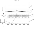
- a color conversion substrate 100 is configured to convert the color (wavelength) of a portion of light emitted by one or more light-emitting diodes (LEDs) used as a backlight source of a display device, for example, a liquid crystal display (LCD).
- the color conversion substrate 100 is disposed to the rear of a display panel 20 such as an LCD panel, and forms, together with one or more LEDs (hereinafter referred to as "LEDs") 10, an LCD backlight unit (BLU) radiating light toward the display panel 20.
- LEDs hereinafter referred to as "LEDs"
- BLU LCD backlight unit
- each of the LEDs 10 may include an LED body and an LED chip.
- the LED body is a structure having a hollow portion in a specific shape, providing a structural space for accommodation of the LED chip.
- the LED body has wires and a lead frame by which the LED chip is electrically connected to an external power source.
- the LED chip is a light source emitting light when an electrical current is applied thereto by the external power source, is mounted on the LED body, and is connected to the external power source via the wires and the lead frame.
- the LED chip is implemented as a forward junction of an n-semiconductor layer that provides electrons and a p-semiconductor layer that provides holes.
- the backlight unit is implemented as a side emitting backlight. Accordingly, the LEDs 10 are disposed on one side of the color conversion substrate 100 to emit light toward the color conversion substrate 100.
- the color conversion substrate 100 according to the present embodiment forming the backlight unit of the display panel 20 together with the LEDs 10 includes a thin glass plate 110, a quantum dot (QD) coating layer 120, a light guide plate 130, and a sealant 140.
- QD quantum dot
- the thin glass plate 110 protects the QD coating layer 120 disposed on the bottom surface thereof (when referring to FIG. 1 ).
- the thin glass plate 110 serves as a path along which light emitted by the LEDs 10 passes or exits in the direction of the display panel 20 disposed above the thin glass plate 110.
- the thin glass plate 110 is bonded to the light guide plate 130 by the sealant 140, thereby isolating the QD coating layer 120 from the external environment.
- the thin glass plate 110 may formed of a material selected from among, but is not limited to, silicate glass, silica glass, borosilicate glass, and non-alkali glass, with a thickness of 0.3 mm or less. According to the present embodiment, the thin glass plate 110 provided as above can reduce the thickness of the color conversion substrate 100, thereby reducing the thickness of the display device.
- a pattern 111 having an embossed structure is formed on the top surface of the thin glass plate 110, i.e. the surface of the thin glass plate 110 facing the display panel 20.
- the pattern 111 is illustrated as having a semicircular cross-section in the present embodiment, this is merely illustrative, and the pattern 111 may have a variety of cross-sectional shapes.
- the pattern 111 formed on the top surface of the thin glass plate 110 as above can reduce the amount of light that is totally reflected from the interface between the thin glass plate 110 and air while the light is passing through the thin glass plate 110. This can consequently increase the color conversion efficiency of QDs in the QD coating layer 120 and, furthermore, can reduce the number of LEDs 10 used as the light source and the amount of energy consumed, whereby a highly-efficient environmentally-friendly display device can ultimately be realized.
- the QD coating layer 120 is disposed on the bottom surface of the thin glass plate 110.
- the QD coating layer 120 is hermetically sealed by the thin glass plate 110, the light guide plate 130 and the sealant 140, thereby being prevented from being exposed to the air.
- the QDs of the QD coating layer 120 convert the wavelength of light emitted by the LEDs 10, thereby generating wavelength-converted light, i.e. fluorescent light.
- the QD coating layer 120 since the LEDs 10 are implemented as blue LEDs, the QD coating layer 120 may be formed of a QD material converting the wavelength of a portion of light emitted by the blue LEDs 10 into yellow light.
- a pattern 121 having an embossed structure is formed on the bottom surface of the QD coating layer 120, i.e. on the surface of the QD coating layer 120 facing the light guide plate 130.
- the embossed pattern 121 has a triangular cross-section as illustrated in FIG. 1
- the embossed pattern 121 may have a variety of other shapes.
- the shape of the pattern 121 formed on the QD coating layer 120 is not limited to any specific shape.
- the embossed pattern 121 is formed on the bottom surface of the QD coating layer 120 through which light guided by the light guide plate 130 enters the QD coating layer 120, and thus serves to scatter the light to be wavelength-converted by the QD coating layer 120. This consequently enables additional wavelength conversion, thereby improving color conversion efficiency.
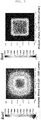
- FIG. 2 illustrates simulated light diffusion patterns demonstrating the effects of the pattern 121 formed on the surface of the QD coating layer 120. It is apparent that light is diffused in the case in which the pattern 121 is formed on the surface of the QD coating layer 120 (left), whereas substantially no light is diffused in the case in which the surface of the QD coating layer is flat (right).
- the light guide plate (LGP) 130 is disposed to face the QD coating layer 120.
- the light guide plate 130 and the thin glass plate 110 are bonded by means of the sealant 140, thereby sealing the QD coating layer 120.
- the light guide plate 130 distributes light that is incident thereto after being emitted by a point light source of the LEDs 10, uniformly over the entire area of the display panel 20. That is, the light guide plate 130 guides the light emitted by the LEDs 10 in the direction of the QD coating layer 120 and the display panel 20.
- the light guide plate 130 may be implemented as a glass light guide plate or a polymer light guide plate.
- the thickness of the light guide plate 130 may be 1.0 mm or less.
- the sealant 140 is disposed between the thin glass plate 110 and the light guide plate 130. Specifically, the sealant 140 is disposed between the bottom periphery of the thin glass plate 110, laterally spaced apart from the QD coating layer 120 on the bottom surface of the thin glass plate 110 and the top periphery of the light guide plate 130 corresponding to the bottom periphery.
- the sealant 140 disposed between the thin glass plate 110 and the light guide plate 130 is in a shape encircling the side surfaces of the QD coating layer 120, serving, together with the thin glass plate 110 and the light guide plate 130, to isolate the QD coating layer 120 from the external environment.
- the sealant 140 may be formed of a frit having superior ability in being bonded to the thin glass plate 110 and the glass light guide plate.
- the sealant 140 may be formed of an epoxy.
- the color conversion substrate 100 may include a moisture absorber 150 within an enclosed space defined by the thin glass plate 110, the sealant 140, and the light guide plate 130.
- the moisture absorber 150 can prevent the QD coating layer 120 from being exposed to moisture, thereby further improving long-term stability of the QD coating layer 120.
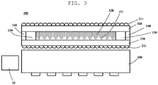
- FIG. 3 is a cross-sectional view schematically illustrating the color conversion substrate according to the another embodiment and a display device including the same.
- a color conversion substrate 200 includes a first thin glass plate 210, a QD coating layer 120, a second thin glass plate 230, a sealant 140, and a light guide plate 240.
- the first thin glass plate 210 may formed of one material selected from among, but is not limited to, silicate glass, silica glass, borosilicate glass, and non-alkali glass, with a thickness of 0.5 mm or less, like the thin glass plate (110 in FIG. 1 ) according to the former embodiment.
- a pattern 211 having an embossed structure is formed on the top surface of the first thin glass plate 210. Descriptions of the functions and effects of the pattern 211 identical to those of the pattern (111 in FIG. 1 ) of the thin glass plate 110 according to the former embodiment will be omitted.
- the QD coating layer 120 is disposed on the bottom layer of the first thin glass plate 210. Descriptions of the QD coating layer 120 identical to the QD coating layer (120 in FIG. 1 ) according to the former embodiment will be omitted.
- the second thin glass plate 230 is in close contact with the bottom surface of the QD coating layer 120.
- the thickness and type of the second thin glass plate 230 may be identical to those of the first thin glass plate 210.
- a pattern 231 having an embossed structure 231 is disposed on the bottom surface of the second thin glass plate 230.
- the pattern 231 faces the light guide plate 240.
- the pattern 231 disposed on the bottom surface of the second thin glass plate 230 facing the light guide plate 240 increases lengths of paths along which light guided by the light guide plate 240 travels. This can consequently increase the contact between the light and the QD coating layer 120, thereby further increasing color conversion efficiency.
- the sealant 140 is disposed between the first thin glass plate 210 and the second thin glass plate 230 in order to isolate the QD coating layer 120 from the external environment.
- the sealant 140 may be formed of a frit having superior ability to be bonded to the first thin glass plate 210 and the second thin glass plate 230.
- the second thin glass plate 230 is bonded to the first thin glass plate 210 by means of the sealant 140, thereby sealing the QD coating layer 120 disposed on the bottom surface of the first thin glass plate 210. Due to this configuration, the light guide plate 240 is disposed under the second thin glass plate 230 in order to guide light emitted by LEDs 10 in the direction of the QD coating layer 120.
- the color conversion substrate 200 includes a moisture absorber 150 disposed between the QD coating layer 120 and the sealant 140.
- FIG. 1 and FIG. 3 will be referred to for the components of the color conversion substrate.
- a QD coating layer 120 is formed by coating a thin glass plate 110 with a paste containing QDs.
- a pattern 121 in an embossed structure may be formed on the surface of the QD coating layer 120 by adjusting the degree of curing the paste.
- a pattern 111 in an embossed structure may be formed on the surface of the thin glass plate 110 facing away from the surface coated with the paste.
- the light guide plate 130 or a second thin glass plate 230 having a pattern 231 is disposed in a position facing the thin glass plate 110 such that the QD coating layer 120 is sandwiched between the light guide plate 130 or the second thin glass plate 230 and the thin glass plate 110.
- a sealant 140 may be applied on the periphery of the thin glass plate 110 laterally spaced apart from the QD coating layer 120 or may be applied on the periphery of the second thin glass plate 230 or the light guide plate 130 that faces the thin glass plate 110.
- a moisture absorber 150 may be applied to on thin glass plate 110 between the QD coating layer 120 and the applied sealant 140, around the QD coating layer 120.
- the thin glass plate 110 and the second thin glass plate 230 or the thin glass plate 110 and the light guide plate 130 are bonded to each other by firing the sealant 140 disposed therebetween, whereby the method of fabricating a color conversion substrate according to the present embodiment is completed.
- the sealant 140 be formed of a frit when bonding the thin glass plate 110 and the second thin glass plate 230 or the thin glass plate 110 and the light guide plate 130 formed of glass. It is preferable that the sealant 140 be formed of an epoxy when bonding the thin glass plate 110 and the light guide plate 130 formed of a polymer.
- the light guide plate 240 is disposed under the thin glass plate 230, whereby light emitted by the LEDs 10 disposed on the side of the light guide plate 240 is guided to the QD coating layer 120.
Landscapes
- Physics & Mathematics (AREA)
- Spectroscopy & Molecular Physics (AREA)
- General Physics & Mathematics (AREA)
- Optics & Photonics (AREA)
- Engineering & Computer Science (AREA)
- General Engineering & Computer Science (AREA)
- Nonlinear Science (AREA)
- Chemical & Material Sciences (AREA)
- Crystallography & Structural Chemistry (AREA)
- Microelectronics & Electronic Packaging (AREA)
- Mathematical Physics (AREA)
- Led Device Packages (AREA)
- Planar Illumination Modules (AREA)
- Liquid Crystal (AREA)
- Optical Filters (AREA)
Applications Claiming Priority (2)
| Application Number | Priority Date | Filing Date | Title |
|---|---|---|---|
| KR1020140130971A KR20160038325A (ko) | 2014-09-30 | 2014-09-30 | 색변환용 기판, 그 제조방법 및 이를 포함하는 디스플레이 장치 |
| PCT/KR2015/008278 WO2016052856A1 (ko) | 2014-09-30 | 2015-08-07 | 색변환용 기판, 그 제조방법 및 이를 포함하는 디스플레이 장치 |
Publications (2)
| Publication Number | Publication Date |
|---|---|
| EP3203280A1 true EP3203280A1 (de) | 2017-08-09 |
| EP3203280A4 EP3203280A4 (de) | 2018-05-02 |
Family
ID=55630848
Family Applications (1)
| Application Number | Title | Priority Date | Filing Date |
|---|---|---|---|
| EP15848034.3A Withdrawn EP3203280A4 (de) | 2014-09-30 | 2015-08-07 | Substrat zur farbumwandlung, herstellungsverfahren dafür und anzeigevorrichtung damit |
Country Status (7)
| Country | Link |
|---|---|
| US (1) | US10215907B2 (de) |
| EP (1) | EP3203280A4 (de) |
| JP (1) | JP6623427B2 (de) |
| KR (1) | KR20160038325A (de) |
| CN (1) | CN107077028A (de) |
| TW (1) | TWI604239B (de) |
| WO (1) | WO2016052856A1 (de) |
Families Citing this family (21)
| Publication number | Priority date | Publication date | Assignee | Title |
|---|---|---|---|---|
| DE102014117983A1 (de) * | 2014-12-05 | 2016-06-09 | Osram Opto Semiconductors Gmbh | Konversionselement, optoelektronisches Halbleiterbauelement und Verfahren zur Herstellung von Konversionselementen |
| KR102260013B1 (ko) * | 2014-12-10 | 2021-06-04 | 삼성디스플레이 주식회사 | 표시 장치 및 이의 제조 방법 |
| EP3279709A4 (de) * | 2015-04-02 | 2018-10-03 | Toppan Printing Co., Ltd. | Quantenpunktschutzfolie und wellenlängenumwandlungsfolie und damit hergestellte hintergrundbeleuchtungseinheit |
| CN105810796A (zh) * | 2016-04-21 | 2016-07-27 | 深圳市华星光电技术有限公司 | 一种量子点材料玻璃板及其制作方法 |
| KR102627073B1 (ko) * | 2016-11-30 | 2024-01-19 | 삼성디스플레이 주식회사 | 백라이트 유닛, 표시 장치 및 표시 장치의 제조 방법 |
| KR102439084B1 (ko) | 2017-08-29 | 2022-09-02 | 삼성디스플레이 주식회사 | 표시 장치의 제조 방법 |
| CN108196336B (zh) | 2018-01-02 | 2020-06-30 | 京东方科技集团股份有限公司 | 一种导光板、背光模组、显示装置 |
| US20190219874A1 (en) * | 2018-01-16 | 2019-07-18 | Huizhou China Star Optoelectronics Technology Co., Ltd. | Backlight module and display device |
| WO2019177755A1 (en) * | 2018-03-13 | 2019-09-19 | Apple Inc. | Displays with direct-lit backlight units |
| KR102568654B1 (ko) | 2018-04-10 | 2023-08-23 | 삼성디스플레이 주식회사 | 백라이트 유닛, 백라이트 유닛을 포함하는 표시 장치 및 표시 장치를 제조하는 방법 |
| KR102537268B1 (ko) * | 2018-04-23 | 2023-05-30 | 삼성디스플레이 주식회사 | 표시 장치 |
| US10524666B2 (en) * | 2018-05-09 | 2020-01-07 | Inner Ray, Inc. | White excitation light generating device and white excitation light generating method |
| CN108807619A (zh) * | 2018-06-05 | 2018-11-13 | 福州大学 | 一种基于发光材料的qdef显示装置 |
| KR20200076770A (ko) | 2018-12-19 | 2020-06-30 | 삼성디스플레이 주식회사 | 광변환층 조성물, 광변환층 및 이를 포함하는 전자 장치 |
| CN109499837B (zh) | 2018-12-29 | 2023-08-29 | 新疆天研种子机械工程技术研究中心(有限公司) | 一种辣椒清选分离系统 |
| CN109755268A (zh) * | 2018-12-29 | 2019-05-14 | 武汉华星光电技术有限公司 | 一种色转换层及其制作方法、显示面板 |
| WO2021240655A1 (ja) * | 2020-05-26 | 2021-12-02 | シャープ株式会社 | 発光素子及び発光素子の製造方法 |
| US11526051B2 (en) | 2021-04-16 | 2022-12-13 | Apple Inc. | Displays with direct-lit backlight units |
| US11333924B1 (en) | 2021-04-16 | 2022-05-17 | Apple Inc. | Displays with direct-lit backlight units |
| US11513392B1 (en) | 2021-09-23 | 2022-11-29 | Apple Inc. | Direct-lit backlight units with optical films |
| KR102927440B1 (ko) * | 2022-06-09 | 2026-02-12 | 삼성에스디아이 주식회사 | 디스플레이 장치 |
Family Cites Families (25)
| Publication number | Priority date | Publication date | Assignee | Title |
|---|---|---|---|---|
| KR20040090667A (ko) * | 2003-04-18 | 2004-10-26 | 삼성전기주식회사 | 디스플레이용 라이트 유닛 |
| KR100735148B1 (ko) * | 2004-11-22 | 2007-07-03 | (주)케이디티 | 백라이트 장치용 광 여기 확산시트, 이를 이용한액정표시용 백라이트 장치 |
| JP4955422B2 (ja) * | 2006-03-08 | 2012-06-20 | 三菱電機株式会社 | 発光装置 |
| ITMI20071238A1 (it) * | 2007-06-20 | 2008-12-21 | Getters Spa | Led bianchi o ultravioletti contenenti un sistema getter |
| JP2010533976A (ja) * | 2007-07-18 | 2010-10-28 | キユーデイー・ビジヨン・インコーポレーテツド | 固体照明に有用な量子ドットベースの光シート |
| JP2009231273A (ja) * | 2008-02-27 | 2009-10-08 | Seiko Instruments Inc | 照明装置及びこれを備える表示装置 |
| WO2011044391A1 (en) * | 2009-10-07 | 2011-04-14 | Qd Vision, Inc. | Device including quantum dots |
| JP5418762B2 (ja) * | 2008-04-25 | 2014-02-19 | ソニー株式会社 | 発光装置および表示装置 |
| KR101154368B1 (ko) * | 2010-09-27 | 2012-06-15 | 엘지이노텍 주식회사 | 광변환부재 제조방법 및 그 제조방법으로 제조된 광변환부재를 포함하는 백라이트 유닛 |
| KR101210158B1 (ko) * | 2010-11-04 | 2012-12-07 | 엘지이노텍 주식회사 | 표시장치 및 광 변환 부재 |
| EP2638321B1 (de) * | 2010-11-10 | 2019-05-08 | Nanosys, Inc. | Quantenpunktfilme, beleuchtungsvorrichtungen und beleuchtungsverfahren |
| KR20120088273A (ko) | 2011-01-31 | 2012-08-08 | 엘지이노텍 주식회사 | 백라이트 유닛 및 그 제조 방법 |
| KR101210180B1 (ko) * | 2011-04-21 | 2012-12-07 | 엘지이노텍 주식회사 | 광학 부재 및 이의 제조방법 |
| KR101221921B1 (ko) * | 2011-07-05 | 2013-01-15 | 엘지전자 주식회사 | 이동 단말기 |
| KR20130009020A (ko) * | 2011-07-14 | 2013-01-23 | 엘지이노텍 주식회사 | 광학 부재, 이를 포함하는 표시장치 및 이의 제조방법 |
| KR101893494B1 (ko) * | 2011-07-18 | 2018-08-30 | 엘지이노텍 주식회사 | 광학 부재 및 이를 포함하는 표시장치 |
| JP2013033833A (ja) * | 2011-08-01 | 2013-02-14 | Panasonic Corp | 波長変換膜及びそれを用いた発光装置並びに照明装置 |
| KR101338695B1 (ko) * | 2012-04-27 | 2013-12-06 | 엘지이노텍 주식회사 | 표시 장치, 광 변환 부재 및 광 변환 부재 제조 방법 |
| JPWO2014024218A1 (ja) * | 2012-08-06 | 2016-07-21 | パナソニックIpマネジメント株式会社 | 蛍光体光学素子、その製造方法及び光源装置 |
| KR101426448B1 (ko) * | 2012-11-09 | 2014-08-05 | 주식회사 엘엠에스 | 나노 복합체, 이를 포함하는 광학 부재 및 백라이트 유닛 |
| CN104019401A (zh) * | 2013-02-28 | 2014-09-03 | 联想(北京)有限公司 | 一种背光模组、双显屏结构以及电子设备 |
| WO2014147690A1 (ja) * | 2013-03-18 | 2014-09-25 | 富士通株式会社 | モジュール型データセンター |
| KR102126176B1 (ko) * | 2014-02-05 | 2020-06-25 | 삼성디스플레이 주식회사 | 파장 변환 부재 및 그 제조 방법, 및 이를 포함하는 백라이트 어셈블리 |
| KR102140630B1 (ko) * | 2014-02-11 | 2020-08-04 | 삼성디스플레이 주식회사 | 파장 변환 부재 및 그 제조 방법, 및 이를 포함하는 백라이트 어셈블리 |
| US9513426B2 (en) * | 2014-10-22 | 2016-12-06 | Industrial Technology Research Institute | Light down conversion film and display backlight unit using the same |
-
2014
- 2014-09-30 KR KR1020140130971A patent/KR20160038325A/ko not_active Ceased
-
2015
- 2015-08-07 EP EP15848034.3A patent/EP3203280A4/de not_active Withdrawn
- 2015-08-07 WO PCT/KR2015/008278 patent/WO2016052856A1/ko not_active Ceased
- 2015-08-07 JP JP2017517016A patent/JP6623427B2/ja active Active
- 2015-08-07 US US15/515,873 patent/US10215907B2/en active Active
- 2015-08-07 CN CN201580052979.XA patent/CN107077028A/zh active Pending
- 2015-09-30 TW TW104131995A patent/TWI604239B/zh active
Also Published As
| Publication number | Publication date |
|---|---|
| US20170299792A1 (en) | 2017-10-19 |
| JP6623427B2 (ja) | 2019-12-25 |
| US10215907B2 (en) | 2019-02-26 |
| KR20160038325A (ko) | 2016-04-07 |
| TWI604239B (zh) | 2017-11-01 |
| CN107077028A (zh) | 2017-08-18 |
| EP3203280A4 (de) | 2018-05-02 |
| WO2016052856A1 (ko) | 2016-04-07 |
| JP2017532600A (ja) | 2017-11-02 |
| TW201626009A (zh) | 2016-07-16 |
Similar Documents
| Publication | Publication Date | Title |
|---|---|---|
| US10215907B2 (en) | Substrate for color conversion, manufacturing method therefor, and display device comprising same | |
| US9905542B2 (en) | LED light bar manufacturing method and LED light bar | |
| WO2007077869A1 (ja) | 薄型発光ダイオードランプとその製造方法 | |
| KR101555954B1 (ko) | 발광 다이오드의 색변환용 기판 및 그 제조방법 | |
| US20190355783A1 (en) | Led module | |
| CN105805694A (zh) | 一种量子点光源及量子点背光模组 | |
| TW201320406A (zh) | 提升混光效果之白光二極體封裝改良結構 | |
| US20170244009A1 (en) | Substrate for color conversion of light-emitting diode and manufacturing method therefor | |
| US9893248B2 (en) | Substrate for changing color of light emitting diode and method for producing same | |
| US10141481B2 (en) | Color-converting substrate of light-emitting diode and method for producing same | |
| JP4943005B2 (ja) | 薄型発光ダイオードランプとその製造方法 | |
| KR20150138606A (ko) | 발광 소자 모듈 | |
| CN110676364B (zh) | 一种四面出光蓝光波导面发光结构 | |
| KR20130074326A (ko) | 파장변환층이 형성된 발광소자 제조방법 및 그에 따라 제조된 발광소자 | |
| KR100600411B1 (ko) | 발광 소자 패키지 및 그의 제조 방법 | |
| KR102160774B1 (ko) | 발광 소자 패키지 및 그 제조방법 | |
| KR20150034040A (ko) | 백라이트 패널 어셈블리 | |
| US8878216B2 (en) | Light emitting diode module and method for manufacturing the same | |
| KR102475623B1 (ko) | 발광 장치 | |
| KR20120045876A (ko) | 발광소자 패키지 및 그 제조방법 | |
| KR20120045405A (ko) | 발광소자 패키지 어레이 | |
| JP2016139833A (ja) | 発光装置 | |
| KR20120046394A (ko) | 발광소자 패키지 | |
| TWM493157U (zh) | 提升混光效果之白光二極體封裝改良結構 |
Legal Events
| Date | Code | Title | Description |
|---|---|---|---|
| STAA | Information on the status of an ep patent application or granted ep patent |
Free format text: STATUS: THE INTERNATIONAL PUBLICATION HAS BEEN MADE |
|
| PUAI | Public reference made under article 153(3) epc to a published international application that has entered the european phase |
Free format text: ORIGINAL CODE: 0009012 |
|
| STAA | Information on the status of an ep patent application or granted ep patent |
Free format text: STATUS: REQUEST FOR EXAMINATION WAS MADE |
|
| 17P | Request for examination filed |
Effective date: 20170330 |
|
| AK | Designated contracting states |
Kind code of ref document: A1 Designated state(s): AL AT BE BG CH CY CZ DE DK EE ES FI FR GB GR HR HU IE IS IT LI LT LU LV MC MK MT NL NO PL PT RO RS SE SI SK SM TR |
|
| AX | Request for extension of the european patent |
Extension state: BA ME |
|
| DAV | Request for validation of the european patent (deleted) | ||
| DAX | Request for extension of the european patent (deleted) | ||
| A4 | Supplementary search report drawn up and despatched |
Effective date: 20180405 |
|
| RIC1 | Information provided on ipc code assigned before grant |
Ipc: G02F 1/1335 20060101ALN20180329BHEP Ipc: G02F 1/13357 20060101AFI20180329BHEP Ipc: F21V 8/00 20060101ALI20180329BHEP |
|
| STAA | Information on the status of an ep patent application or granted ep patent |
Free format text: STATUS: EXAMINATION IS IN PROGRESS |
|
| 17Q | First examination report despatched |
Effective date: 20200507 |
|
| STAA | Information on the status of an ep patent application or granted ep patent |
Free format text: STATUS: THE APPLICATION IS DEEMED TO BE WITHDRAWN |
|
| 18D | Application deemed to be withdrawn |
Effective date: 20240301 |