EP3203298A1 - Dispositif d'entraînement de miroir et son procédé d'entraînement - Google Patents
Dispositif d'entraînement de miroir et son procédé d'entraînement Download PDFInfo
- Publication number
- EP3203298A1 EP3203298A1 EP15847123.5A EP15847123A EP3203298A1 EP 3203298 A1 EP3203298 A1 EP 3203298A1 EP 15847123 A EP15847123 A EP 15847123A EP 3203298 A1 EP3203298 A1 EP 3203298A1
- Authority
- EP
- European Patent Office
- Prior art keywords
- piezoelectric
- actuator
- mirror
- piezoelectric conversion
- electrode
- Prior art date
- Legal status (The legal status is an assumption and is not a legal conclusion. Google has not performed a legal analysis and makes no representation as to the accuracy of the status listed.)
- Granted
Links
Images





Classifications
-
- G—PHYSICS
- G02—OPTICS
- G02B—OPTICAL ELEMENTS, SYSTEMS OR APPARATUS
- G02B26/00—Optical devices or arrangements for the control of light using movable or deformable optical elements
- G02B26/08—Optical devices or arrangements for the control of light using movable or deformable optical elements for controlling the direction of light
- G02B26/10—Scanning systems
- G02B26/105—Scanning systems with one or more pivoting mirrors or galvano-mirrors
-
- G—PHYSICS
- G02—OPTICS
- G02B—OPTICAL ELEMENTS, SYSTEMS OR APPARATUS
- G02B26/00—Optical devices or arrangements for the control of light using movable or deformable optical elements
- G02B26/08—Optical devices or arrangements for the control of light using movable or deformable optical elements for controlling the direction of light
-
- G—PHYSICS
- G02—OPTICS
- G02B—OPTICAL ELEMENTS, SYSTEMS OR APPARATUS
- G02B26/00—Optical devices or arrangements for the control of light using movable or deformable optical elements
- G02B26/08—Optical devices or arrangements for the control of light using movable or deformable optical elements for controlling the direction of light
- G02B26/0816—Optical devices or arrangements for the control of light using movable or deformable optical elements for controlling the direction of light by means of one or more reflecting elements
- G02B26/0833—Optical devices or arrangements for the control of light using movable or deformable optical elements for controlling the direction of light by means of one or more reflecting elements the reflecting element being a micromechanical device, e.g. a MEMS mirror, DMD
- G02B26/0858—Optical devices or arrangements for the control of light using movable or deformable optical elements for controlling the direction of light by means of one or more reflecting elements the reflecting element being a micromechanical device, e.g. a MEMS mirror, DMD the reflecting means being moved or deformed by piezoelectric means
-
- G—PHYSICS
- G02—OPTICS
- G02B—OPTICAL ELEMENTS, SYSTEMS OR APPARATUS
- G02B26/00—Optical devices or arrangements for the control of light using movable or deformable optical elements
- G02B26/08—Optical devices or arrangements for the control of light using movable or deformable optical elements for controlling the direction of light
- G02B26/10—Scanning systems
-
- H—ELECTRICITY
- H10—SEMICONDUCTOR DEVICES; ELECTRIC SOLID-STATE DEVICES NOT OTHERWISE PROVIDED FOR
- H10N—ELECTRIC SOLID-STATE DEVICES NOT OTHERWISE PROVIDED FOR
- H10N30/00—Piezoelectric or electrostrictive devices
- H10N30/20—Piezoelectric or electrostrictive devices with electrical input and mechanical output, e.g. functioning as actuators or vibrators
- H10N30/204—Piezoelectric or electrostrictive devices with electrical input and mechanical output, e.g. functioning as actuators or vibrators using bending displacement, e.g. unimorph, bimorph or multimorph cantilever or membrane benders
- H10N30/2041—Beam type
- H10N30/2042—Cantilevers, i.e. having one fixed end
- H10N30/2043—Cantilevers, i.e. having one fixed end connected at their free ends, e.g. parallelogram type
-
- H—ELECTRICITY
- H10—SEMICONDUCTOR DEVICES; ELECTRIC SOLID-STATE DEVICES NOT OTHERWISE PROVIDED FOR
- H10N—ELECTRIC SOLID-STATE DEVICES NOT OTHERWISE PROVIDED FOR
- H10N30/00—Piezoelectric or electrostrictive devices
- H10N30/20—Piezoelectric or electrostrictive devices with electrical input and mechanical output, e.g. functioning as actuators or vibrators
- H10N30/208—Piezoelectric or electrostrictive devices with electrical input and mechanical output, e.g. functioning as actuators or vibrators using shear or torsion displacement, e.g. d15 type devices
-
- H—ELECTRICITY
- H10—SEMICONDUCTOR DEVICES; ELECTRIC SOLID-STATE DEVICES NOT OTHERWISE PROVIDED FOR
- H10N—ELECTRIC SOLID-STATE DEVICES NOT OTHERWISE PROVIDED FOR
- H10N30/00—Piezoelectric or electrostrictive devices
- H10N30/30—Piezoelectric or electrostrictive devices with mechanical input and electrical output, e.g. functioning as generators or sensors
- H10N30/302—Sensors
-
- H—ELECTRICITY
- H10—SEMICONDUCTOR DEVICES; ELECTRIC SOLID-STATE DEVICES NOT OTHERWISE PROVIDED FOR
- H10N—ELECTRIC SOLID-STATE DEVICES NOT OTHERWISE PROVIDED FOR
- H10N30/00—Piezoelectric or electrostrictive devices
- H10N30/80—Constructional details
- H10N30/85—Piezoelectric or electrostrictive active materials
- H10N30/853—Ceramic compositions
- H10N30/8548—Lead-based oxides
- H10N30/8554—Lead-zirconium titanate [PZT] based
-
- H—ELECTRICITY
- H10—SEMICONDUCTOR DEVICES; ELECTRIC SOLID-STATE DEVICES NOT OTHERWISE PROVIDED FOR
- H10N—ELECTRIC SOLID-STATE DEVICES NOT OTHERWISE PROVIDED FOR
- H10N30/00—Piezoelectric or electrostrictive devices
- H10N30/101—Piezoelectric or electrostrictive devices with electrical and mechanical input and output, e.g. having combined actuator and sensor parts
-
- H—ELECTRICITY
- H10—SEMICONDUCTOR DEVICES; ELECTRIC SOLID-STATE DEVICES NOT OTHERWISE PROVIDED FOR
- H10N—ELECTRIC SOLID-STATE DEVICES NOT OTHERWISE PROVIDED FOR
- H10N30/00—Piezoelectric or electrostrictive devices
- H10N30/20—Piezoelectric or electrostrictive devices with electrical input and mechanical output, e.g. functioning as actuators or vibrators
- H10N30/204—Piezoelectric or electrostrictive devices with electrical input and mechanical output, e.g. functioning as actuators or vibrators using bending displacement, e.g. unimorph, bimorph or multimorph cantilever or membrane benders
- H10N30/2041—Beam type
-
- H—ELECTRICITY
- H10—SEMICONDUCTOR DEVICES; ELECTRIC SOLID-STATE DEVICES NOT OTHERWISE PROVIDED FOR
- H10N—ELECTRIC SOLID-STATE DEVICES NOT OTHERWISE PROVIDED FOR
- H10N30/00—Piezoelectric or electrostrictive devices
- H10N30/80—Constructional details
- H10N30/802—Circuitry or processes for operating piezoelectric or electrostrictive devices not otherwise provided for, e.g. drive circuits
Definitions
- the present invention relates to a mirror driving device and a driving method thereof, and more particularly to a structure of a micromirror device suitable for an optical deflector used for optical scanning and a driving method thereof.
- a microscanner fabricated using a silicon (Si) microfabrication technology (hereinafter referred to as “microelectromechanical system (MEMS) scanner”) is characterized by its small size and low power consumption, and is thus expected to be widely used in applications ranging from a laser projector to an optical diagnostic scanner such as an optical coherence tomograph.
- Si silicon
- MEMS microelectromechanical system
- a piezoelectric driving system which uses the deformation of a piezoelectric body is regarded as having a higher torque density and a smaller size and obtaining a higher scan angle compared to other methods, and is thus considered to be promising.
- resonance driving is mainly used, and at this time, the height of a torque of the piezoelectric driving system is a great advantage.
- JP2009-2978A there is a system in which a torsion bar is connected to a connection part (joining part) in an actuator having a structure in which two cantilevers are connected, and the torsion bar is caused to undergo tilt displacement by driving the cantilever in antiphase ( JP2009-2978A ).
- JOURNAL OF MICROELECTROMECHANICAL SYSTEMS, Vol. 21, 6 (2012), 1303-1310 proposes a structure in which two plate-like actuators disposed on both sides of the rotation axis of a mirror are provided and the actuators are fixed on the rotation axis of the mirror.
- This structure has an advantage that a mirror tilt angle that is obtained during resonance driving is large because the amount of the actuator displaced during static driving is larger than that of the structure of JP2009-2978A .
- the piezoelectric torque cannot be efficiently converted into tilt displacement, and a high voltage of about 25 V is necessary to obtain a sufficient displacement angle.
- a high voltage of about 25 V is necessary to obtain a sufficient displacement angle.
- driving at about 15 V is preferable.
- a sensor stress detection part which monitors the drive displacement.
- one of the actuators needs to be used as a sensor part, which causes a problem that the driving force significantly decreases to about half.
- the present invention has been made taking the foregoing circumstances into consideration, and an object thereof is to provide a mirror driving device and a driving method thereof capable of improving a displacement efficiency compared to a structure in the related art and obtaining a sufficiently large displacement angle even in a case where a sensor part is provided.
- a mirror driving device comprises: a mirror part having a reflecting surface; a mirror support part which is connected to the mirror part and supports the mirror part so as to be rotatable about a rotation axis; a piezoelectric actuator part which is connected to the mirror support part and generates a driving force to rotate the mirror part about the rotation axis; and a fixing part which supports the piezoelectric actuator part, in which the piezoelectric actuator part has a laminated structure in which a vibration plate, a lower electrode, a piezoelectric body, and an upper electrode are laminated in this order, and includes a first actuator part and a second actuator part which are piezoelectric unimorph actuators that are deformed by an inverse piezoelectric effect of the piezoelectric body caused by application of a drive voltage, the first actuator part is disposed on one side of both sides of a direction which is orthogonal to a film thickness direction of the piezoelectric body and is an orthogonal direction of the rotation axis in the ortho
- the upper electrode and the lower electrode are disposed as divided electrode parts to correspond to a direction of stress in the piezoelectric body during driving the piezoelectric actuator part (that is, during displacement). Due to the division arrangement of the electrode parts, driving can be more efficiently performed than in a configuration in the related art.
- a unimorph structure is the simplest configuration. Since a piezoelectric driving system can be driven only by applying a voltage between electrodes, the configuration is simple and is useful for miniaturization.
- the first connection point and the first base end part may be in a positional relationship so as to be distant from the center of the mirror part in this order in the axial direction of the rotation axis
- the second connection point and the second base end part may be in a positional relationship so as to be distant from the center of the mirror part in this order in the axial direction of the rotation axis.
- the mirror driving device of the first aspect or the second aspect may further comprise: a first connection part which is a member that connects the first actuator part to the mirror support part; and a second connection part which is a member that connects the second actuator part to the mirror support part.
- the first actuator part and the second actuator part may be connected to each other, and the mirror support part may be connected to a connection portion between the first actuator part and the second actuator part.
- the first base end part and the second base end part may be connected to each other.
- An integral base end part shape in which the first base end part and the second base end part are integrated with each other can be achieved.
- a drive voltage for piezoelectric driving may be applied to at least one electrode part of the first lower electrode part, the second lower electrode part, the third lower electrode part, or the fourth lower electrode part.
- a first mirror support part and a second mirror support part which support the mirror part from both sides in the axial direction of the rotation axis, may be provided as the mirror support part.
- the first actuator part may have the first base end part at each of end parts on both sides in the axial direction, a movable part that extends from the first base end part at one of the end parts on both sides of the first actuator part to the first base end part at the other thereof may have a shape bypassing the mirror part, the second actuator part may have the second base end part at each of the end parts on both sides in the axial direction, and a movable part that extends from the second base end part at one of the end parts on both sides of the second actuator part to the second base end part at the other thereof may have a shape bypassing the mirror part.
- the mirror part, the mirror support part, the first actuator part, and the second actuator part may have a line symmetrical form with respect to the rotation axis as an axis of symmetry, in a plan view in a non-driven state.
- the mirror part, the mirror support part, the first actuator part, and the second actuator part may have a line symmetrical form with respect to a center line which passes through the center of the mirror part and is orthogonal to the rotation axis as an axis of symmetry, in the plan view in the non-driven state.
- the mirror driving device of any one of the first to tenth aspects may further comprise: a driving circuit which applies a voltage for driving to electrodes constituting at least one of the upper electrode parts of the first piezoelectric conversion part and the third piezoelectric conversion part, and applies a voltage for driving to electrodes constituting at least one of the lower electrode parts of the second piezoelectric conversion part and the fourth piezoelectric conversion part, in which the drive voltage applied to the electrodes constituting at least one of the upper electrode parts of the first piezoelectric conversion part and the third piezoelectric conversion part, and the drive voltage applied to the electrodes constituting at least one of the lower electrode parts of the second piezoelectric conversion part and the fourth piezoelectric conversion part may be in phase.
- a driving circuit which applies a voltage for driving to electrodes constituting at least one of the upper electrode parts of the first piezoelectric conversion part and the third piezoelectric conversion part, and applies a voltage for driving to electrodes constituting at least one of the lower electrode parts of the second piezoelectric
- some of the electrodes of the upper electrode part and the lower electrode part of each of the first piezoelectric conversion part, the second piezoelectric conversion part, the third piezoelectric conversion part, and the fourth piezoelectric conversion part may be set to be at a floating potential, and a detection circuit which detects a voltage generated by a piezoelectric effect accompanied with deformation of the piezoelectric body from the electrode at the floating potential may be provided.
- the mirror driving device of any one of the first to twelfth aspects may further comprise: a driving circuit which supplies a drive voltage to the piezoelectric actuator part, in which the driving circuit may supply a voltage waveform of the drive voltage for causing the mirror part to undergo resonance driving.
- the piezoelectric body used in the piezoelectric actuator part may be a thin film having a thickness of 1 to 10 ⁇ m and may be a thin film directly formed on a substrate which serves as a vibration plate.
- a piezoelectric thin film having required piezoelectric performance can be obtained.
- a direct film formation method such as a vapor deposition method represented by a sputtering method or a sol-gel method.
- the piezoelectric body used in the piezoelectric actuator part may be one or two or more perovskite type oxides represented by the following general formula (P-1).
- P-1 general formula ABO 3 ... (P-1) in the formula, A is an element in A-site and is at least one element including Pb.
- the molar ratio among the A-site element, the B-site element, and the oxygen element is 1 : 1 : 3 as a standard, and the molar ratio may be deviated from the reference molar ratio within a range in which a perovskite structure is able to be achieved.
- the piezoelectric body used in the piezoelectric actuator part may be one or two or more perovskite type oxides represented by the following general formula (P-2), General formula A a (Zr x ,Ti y ,M b-x-y ) b O c ... (P-2) in the formula, A is an element in A-site and is at least one element including Pb.
- PZT doped with an element such as Nb has a high piezoelectric constant and is thus suitable for fabrication of a device which has a small size and can achieve large displacement.
- the same piezoelectric material as that of the piezoelectric actuator part may be used.
- the perovskite type oxide (P-2) may include Nb, and the molar ratio Nb / (Zr + Ti + Nb) may be 0.06 or more and 0.20 or less.
- Such a material exhibits good piezoelectric characteristics even when a polarization treatment is not performed thereon. Therefore, the polarization treatment is unnecessary, simplification and a reduction in costs of the production process can be realized.
- a mirror driving method is a mirror driving method in the mirror driving device of any one of the first to seventeenth aspects, and comprises: applying a first drive voltage to an electrode constituting at least one piezoelectric conversion part of the first piezoelectric conversion part or the third piezoelectric conversion part; and applying a second drive voltage, which is in phase with the first drive voltage, to an electrode constituting at least one piezoelectric conversion part of the second piezoelectric conversion part or the fourth piezoelectric conversion part, thereby causing the first actuator part and the second actuator part to bend in opposite directions.
- some of the electrodes of the upper electrode parts and the lower electrode parts of each of the first piezoelectric conversion part, the second piezoelectric conversion part, the third piezoelectric conversion part, and the fourth piezoelectric conversion part may be used as a detection electrode which detects a voltage generated by a piezoelectric effect accompanied with deformation of the piezoelectric body, and a detection signal may be obtained from the detection electrodes during driving of the mirror part, in the mirror driving method of the eighteenth aspect.
- At least one of the frequency (driving frequency) or the amplitude of the drive voltage supplied to the piezoelectric actuator part can be controlled on the basis of the detection signal obtained from the detection electrode.
- Stable resonance driving can be realized by feeding back the detection signal to drive the piezoelectric actuator part.
- the electrode parts are disposed according to the distribution of the stresses generated in the piezoelectric body during the deformation of the actuator parts, driving can be efficiently performed, and a larger mirror tilt angle can be obtained compared to the configuration in the related art. Furthermore, since the displacement efficiency is improved, even in a case where some of the electrodes are used for detection, a sufficient displacement angle can be obtained.
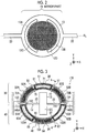
- Fig. 1 is a plan view illustrating a configuration of a micromirror device according to a first embodiment.
- the micromirror device 10 comprises a mirror part 12, a mirror support part 14, a piezoelectric actuator part 16, and a fixing frame 18.
- the micromirror device 10 corresponds to a form of "mirror driving device".
- the upper surface of the mirror part 12 is a reflecting surface 12C that reflects light.
- a metal thin film such as Au (gold) or Al (aluminum) is formed on the reflecting surface 12C in order to increase the reflectance of incident rays.
- Materials and film thicknesses used for mirror coating are not particularly limited, and various designs are possible using well-known mirror materials (high reflectance materials).
- the shape in the plan view of the mirror part 12 that functions as the reflecting part and the shape of the reflecting surface 12C which is a mirror coated region may be coincident with each other or may be different from each other.
- the reflecting surface 12C can be formed within the area range of the upper surface of the mirror part 12.
- the mirror support part 14 is connected to the mirror part 12, and supports the mirror part 12 so as to be rotatable about a rotation axis R A .
- the mirror support part 14 is constituted by a first torsion bar part 20 and a second torsion bar part 22.
- the first torsion bar part 20 and the second torsion bar part 22 support the mirror part 12 from both sides in the axial direction of the rotation axis R A with respect to the mirror part 12.
- the first torsion bar part 20 corresponds to a form of "first mirror support part”
- the second torsion bar part 22 corresponds to a form of "second mirror support part”.
- the piezoelectric actuator part 16 is connected to the mirror support part 14, and generates a driving force to rotate the mirror part 12 about the rotation axis R A .
- the fixing frame 18 is a member that supports the piezoelectric actuator part 16. Since the mirror part 12 is supported by the piezoelectric actuator part 16 via the mirror support part 14, the fixing frame 18 functions as a member that indirectly supports the mirror part 12 via the piezoelectric actuator part 16. In addition, in the fixing frame 18, wiring and electronic circuits (not illustrated) are provided.
- a direction normal to the reflecting surface 12C (a direction perpendicular to Fig. 1 ) in a case where the piezoelectric actuator part 16 is in a non-driven state is defined as a z-axis direction.
- the z-axis direction is the film thickness direction of a piezoelectric body in the piezoelectric actuator part 16.
- a direction parallel to a principal axis which is the rotation axis R A of the mirror part 12 rotated by the first torsion bar part 20 and the second torsion bar part 22 (horizontal direction parallel to Fig. 1 ) is defined as an x-axis direction.
- a direction orthogonal to both the x-axis and the z-axis is defined as a y-axis direction.
- the x-axis direction is the axial direction of the rotation axis R A and may be referred to as a "rotation axis direction" in some cases.
- the y-axis direction is an orthogonal direction orthogonal to the axial direction of the rotation axis R A and may be referred to a "rotation axis orthogonal direction" in some cases.
- the micromirror device 10 has a substantially line symmetrical structure (horizontally symmetrical in Fig. 1 ) with respect to a center line CL which is parallel to the y-axis and passes through the center of the mirror part 12, as an axis of symmetry. Furthermore, the micromirror device 10 has a substantially line symmetrical structure (vertically symmetrical in Fig. 1 ) with the rotation axis R A as an axis of symmetry.
- the mirror part 12 of this example has a rectangular shape in a plan view.
- the shape of the mirror part 12 is not particularly limited.
- the shape is not limited to the rectangular shape illustrated in Fig. 1 , and there are various shapes including a circular shape, an elliptical shape, a square shape, a polygonal shape, and the like.
- the representation of a rectangular shape, a circular shape, an elliptical shape, a square shape, a polygonal shape, or the like is not limited to a shape based on the strict mathematical definition, and means a shape that can be substantially recognized as such a shape as an overall basic shape.
- the concept of the term "quadrangle” includes rectangles with chamfered corner parts, those with round corner parts, those in which some or all of the sides are formed as a curved line or broken line, or those in which additional shapes necessary for connection are added to a connection portion between the mirror part 12 and the mirror support part 14. The same is applied to the representation of the other shapes.
- a deformation prevention frame which suppresses dynamic deformation of the reflecting surface during scan driving.
- a deformation prevention frame 13 isolated from the outline of a reflecting part 12D having the reflecting surface 12C, the dynamic deformation of the reflecting surface 12C during scan driving can be significantly reduced.
- the combined structure of the deformation prevention frame 13 and the reflecting part 12D may be regarded as a "mirror part".
- the mirror part in Fig. 2 is denoted by reference numeral 15.
- the mirror part 15 has a structure in which the first torsion bar part 20 and the second torsion bar part 22 are connected to the deformation prevention frame 13 with slots 13A and 13B formed along the outer edge of the reflecting part 12D interposed therebetween.
- the mirror part 15 as illustrated in Fig. 2 can be employed.
- the piezoelectric actuator part 16 comprises a first actuator part 30 and a second actuator part 40.
- the first actuator part 30 and the second actuator part 40 are separately disposed on both sides in the y-axis direction orthogonal to the axial direction of the rotation axis R A , with respect to the rotation axis R A .
- the upper half of the piezoelectric actuator part 16 in Fig. 1 is the first actuator part 30, and the lower half is the second actuator part 40. That is, the first actuator part 30 is disposed on one side among regions divided by the rotation axis R A into both sides (upper and lower sides in Fig.
- the y-axis direction corresponds to "an orthogonal direction which is a direction orthogonal to the film thickness direction of the piezoelectric body and orthogonal to the axial direction of the rotation axis".
- the first actuator part 30 is connected to one end of the first torsion bar part 20 via a connection part 32.
- the other end of the first torsion bar part 20 is connected to the mirror part 12.
- the first actuator part 30 is connected to one end of the second torsion bar part 22 via a connection part 34.
- the other end of the second torsion bar part 22 is connected to the mirror part 12.
- the connection part 32 and the connection part 34 are members that connect the first actuator part 30 to the mirror support part 14.
- Each of the connection part 32 and the connection part 34 corresponds to a form of a "first connection part".
- connection portion 32A between the first actuator part 30 and the connection part 32 and a connection portion 34A between the first actuator part 30 and the connection part 34 corresponds to a form of a "first connection point”. Otherwise, each of the connection part 32 and the connection part 34 can be interpreted as corresponding to a form of the "first connection point”.
- first base end parts 36A and 36B which are base end parts on both sides in the rotation axis direction (x-axis direction) in the first actuator part 30 is fixed to the fixing frame 18.
- the first actuator part 30 is supported by the fixing frame 18 in a both-end supported beam structure by a configuration in which each of the first base end parts 36A and 36B is fixed to the fixing frame 18.
- both-end supported beam structure is synonymous with "doubly supported beam structure”.
- the fixing frame 18 corresponds to a form of "fixing part".
- the shape of the fixing frame 18 is not limited to the example of Fig. 1 , and various forms of designs are possible.
- the fixing frame 18 may have a function of fixing the respective base end parts of the first actuator part 30 and the second actuator part 40.
- the fixing frame 18 may have a configuration divided into a plurality of members.
- a frame structure divided into two members including a first fixing member to which the first base end part 36A and the second base end part 46A illustrated on the left side of Fig. 1 are fixed, and a second fixing member to which the first base end part 36B and the second base end part 46B illustrated on the right side of Fig. 1 are fixed.
- the first base end part 36A illustrated on the left side of Fig. 1 is positioned on the opposite side of the first actuator part 30 in the x-axis direction to the connection portion 32A for connection of the connection part 32 to the first actuator part 30. That is, in view of a relative positional relationship between the connection portion 32A for connection of the connection part 32 to the first actuator part 30, and the first base end part 36A, the connection portion 32A is positioned on the inside of the first actuator part 30, which is a side close to the mirror part 12 in the x-axis direction, and the first base end part 36A is positioned on the outside of the first actuator part 30, which is a side further away from the mirror part 12 than the connection portion 32A in the x-axis direction.
- the center position of the mirror part 12, the connection portion 32A, and the first base end part 36A are in a positional relationship so as to gradually be distant from the mirror part 12 in this order.
- the first base end part 36B illustrated on the right side of Fig. 1 is positioned on the opposite side of the first actuator part 30 in the x-axis direction to the connection portion 34A for connection of the connection part 34 to the first actuator part 30. That is, the connection portion 34A for connection of the first actuator part 30 to the connection part 34 is positioned on the inside of the first actuator part 30, which is the side close to the mirror part 12 in the x-axis direction, and the first base end part 36B is positioned on the outside of the first actuator part 30, which is the side further away from the mirror part 12 than the connection portion 34A in the x-axis direction.
- the center position of the mirror part 12, the connection portion 34A, and the first base end part 36B are in a positional relationship so as to gradually be distant from the mirror part 12 in this order.
- the first actuator part 30 is a piezoelectric actuator having a both end fixed type both-end supported beam structure in which each of the first base end parts 36A and 36B positioned on both sides in the x-axis direction is restrained by the fixing frame 18.
- Each of the first torsion bar part 20 and the second torsion bar part 22 is connected to the first actuator part 30 in the vicinity of the fixed end of the first actuator part 30, that is, in the vicinity of the first base end parts 36A and 36B, which are root portions where the first actuator part 30 starts to displace.
- connection part 42 is connected to one end of the first torsion bar part 20 via the connection part 42.
- the other end of the second torsion bar part 22 is connected to the mirror part 12.
- the second actuator part 40 is connected to the second torsion bar part 22 via the connection part 44.
- the connection part 42 and the connection part 44 are members that connect the second actuator part 40 to the mirror support part 14.
- Each of the connection part 42 and the connection part 44 corresponds to a form of "second connection part".
- connection portion 42A between the second actuator part 40 and the connection part 42 and the connection portion 44A between the second actuator part 40 and the connection part 44 corresponds to a form of the "second connection point”. Otherwise, each of the connection part 42 and the connection part 44 can be interpreted as corresponding to a form of "second connection point".
- Each of the second base end parts 46A and 46B which are base end parts on both sides in the rotation axis direction (x-axis direction) in the second actuator part 40 is fixed to the fixing frame 18. That is, the second actuator part 40 is supported by the fixing frame 18 in a both-end supported beam structure by a configuration in which each of the second base end parts 46A and 46B is fixed to the fixing frame 18.
- the second base end part 46A illustrated on the left side of Fig. 1 is positioned on the opposite side of the second actuator part 40 in the x-axis direction to the connection portion 42A for connection of the connection part 42 to the second actuator part 40. That is, in view of a relative positional relationship between the connection portion 42A for connection of the connection part 42 to the second actuator part 40, and the second base end part 46A, the connection portion 42A is positioned on the inside of the second actuator part 40, which is the side close to the mirror part 12 in the x-axis direction, and the second base end part 46A is positioned on the outside of the second actuator part 40, which is the side further away from the mirror part 12 than the connection portion 42A in the x-axis direction.
- the center position of the mirror part 12, the connection portion 42A, and the second base end part 46A are in a positional relationship so as to gradually be distant from the mirror part 12 in this order.
- connection portion 44A for connection of the connection part 44 to the connection part 44 is positioned on the inside of the second actuator part 40, which is the side close to the mirror part 12 in the x-axis direction
- second base end part 46A is positioned on the outside of the second actuator part 40, which is the side further away from the mirror part 12 than the connection portion 44A in the x-axis direction.
- the center position of the mirror part 12, the connection portion 44A, and the second base end part 46B are in a positional relationship so as to gradually be distant from the mirror part 12 in this order.
- the second actuator part 40 is a piezoelectric actuator having a both end fixed type both-end supported beam structure in which both the second base end parts 46A and 46B on both sides in the x-axis direction are restrained by the fixing frame 18.
- Each of the first torsion bar part 20 and the second torsion bar part 22 is connected to the second actuator part 40 in the vicinity of the fixed end of the second actuator part 40, that is, in the vicinity of the second base end parts 46A and 46B, which are root portions where the second actuator part 40 starts to displace.
- the first torsion bar part 20 and the second torsion bar part 22 are be moved in a direction in which they rotate about the rotation axis R A , such that the mirror part 12 can be driven to be tilted. That is, by performing driving to bend the first actuator part 30 and the second actuator part 40 in opposite directions, the first torsion bar part 20 and the second torsion bar part 22 are induced to undergo tilt displacement, and the mirror part 12 Is rotated about the rotation axis R A . That is, the reflecting surface 12C of the mirror part 12 is tilted.
- Each of the first actuator part 30 and the second actuator part 40 in this example has an actuator shape with a substantially semicircular arc shape in a plan view, and the two are combined to form the piezoelectric actuator part 16 having a substantially annular shape.
- the piezoelectric actuator part 16 having an external shape with an elliptical ring shape slightly flattened from a true circle is illustrated.
- the actuator shape is not limited to the illustrated example.
- Each of the first actuator part 30 and the second actuator part 40 may have an arcuate actuator shape along a true circle or may have an actuator shape with an elliptical arc shape having a greater oblateness than the example of Fig. 1 .
- an elliptical shape is more preferable than a true circle.
- the first actuator part 30 has, as the upper electrodes thereof, one first upper electrode part 51 and two second upper electrode parts 52A and 52B. That is, the upper electrodes of the first actuator part 30 has an electrode arrangement structure in an electrode division form divided into the first upper electrode part 51 and the second upper electrode parts 52A and 52B with respect to the longitudinal direction of a beam along the shape of a movable part 38 corresponding to a portion of the beam (beam) that connects the one first base end part 36A and the other first base end part 36B.
- the first upper electrode part 51 and the second upper electrode parts 52A and 52B are electrodes that are independent (that is, insulated and separated) from each other.
- the first actuator part 30 When a length direction along the shape of the movable part 38 from the one first base end part 36A to the other first base end part 36B in the first actuator part 30 is referred to as the "length direction of the first actuator part 30", the first actuator part 30 has a structure in which the second upper electrode part 52A, the first upper electrode part 51, and the second upper electrode part 52B are sequentially arranged side by side along the length direction of the first actuator part 30 from the left in Fig. 1 .
- An insulating part 55 is interposed between the second upper electrode part 52A and the first upper electrode part 51.
- An insulating part 57 is interposed between the first upper electrode part 51 and the second upper electrode part 52B.
- the lower electrodes of the first actuator part 30 are also divided into the same division form corresponding to the electrode division form of the upper electrodes. That is, the first actuator part 30 has a first lower electrode part 71 and second lower electrode parts 72A and 72B as the lower electrodes which respectively oppose the first upper electrode part 51 and the second upper electrode parts 52A and 52B.
- the first actuator part 30 has an electrode arrangement structure in which the second lower electrode part 72A, the first lower electrode part 71, and the second lower electrode part 72B are sequentially arranged side by side along the length direction of the first actuator part 30 from the left in Fig. 1 .
- the first lower electrode part 71 and the second lower electrode parts 72A, 72B are electrodes that are independent (that is, insulated and separated) from each other.
- a first piezoelectric conversion part 81 is formed by a laminated structure in which a piezoelectric body (see reference numeral 166 in Fig. 4 ) is interposed between the first upper electrode part 51 and the first lower electrode part 71.
- a pair of the first upper electrode part 51 and the first lower electrode part 71 functions as an electrode pair.
- second piezoelectric conversion parts 82A and 82B are formed by a laminated structure in which piezoelectric bodies are interposed between the second upper electrode parts 52A and 52B and the second lower electrode parts 72A and 72B, respectively.
- a pair of the second upper electrode part 52A and the second lower electrode part 72A functions as an electrode pair
- a pair of the second upper electrode part 52B and the second lower electrode part 72B functions as an electrode pair.
- the second actuator part 40 also has the same structure as the first actuator part 30.
- the second actuator part 40 has, as the upper electrodes thereof, two third upper electrode parts 63A and 63B and one fourth upper electrode part 64. That is, the upper electrodes of the second actuator part 40 has an electrode arrangement structure in an electrode division form divided into the third upper electrode parts 63A and 63B and the fourth upper electrode part 64 with respect to the longitudinal direction of a beam along the shape of a movable part 48 corresponding to a portion of the beam (beam) that connects the one second base end part 46A and the other second base end part 46B.
- the third upper electrode parts 63A and 63B and the fourth upper electrode part 64 are electrodes which are independent (that is, insulated and separated) from each other.
- the second actuator part 40 has a structure in which the third upper electrode part 63A, the fourth upper electrode part 64, and the third upper electrode part 63B are sequentially arranged side by side along the length direction of the second actuator part 40 from the left in Fig. 1 .
- An insulating part 65 is interposed between the third upper electrode part 63A and the fourth upper electrode part 64.
- An insulating part 67 is interposed between the fourth upper electrode part 64 and the third upper electrode part 63B.
- the lower electrodes of the second actuator part 40 are also divided into the same division form corresponding to the electrode division form of the upper electrodes. That is, the second actuator part 40 has third lower electrode parts 93A and 93B and a fourth lower electrode part 94 as the lower electrodes which respectively oppose the electrode parts of the third upper electrode parts 63A and 63B and the fourth upper electrode part 64 with piezoelectric bodies interposed therebetween.
- the second actuator part 40 has an electrode arrangement structure in which the third lower electrode part 93A, the fourth lower electrode part 94, and the third lower electrode part 93B are sequentially arranged side by side along the length direction of the second actuator part 40 from the left in Fig. 1 .
- the third lower electrode parts 93A, 93B and the fourth lower electrode part 94 are electrodes that are independent (that is, insulated and separated) from each other.
- Third piezoelectric conversion parts 103A and 103B are formed by a laminated structure in which piezoelectric bodies are interposed between the third upper electrode parts 63A and 63B and the third lower electrode parts 93A and 93B.
- a pair of the third upper electrode part 63A and the third lower electrode part 93A functions as an electrode pair
- a pair of the third upper electrode part 63B and the third lower electrode part 93B function as an electrode pair.
- a fourth piezoelectric conversion part 104 is formed by a laminated structure in which a piezoelectric body is interposed between the fourth upper electrode part 64 and the fourth lower electrode part 94.
- a pair of the fourth upper electrode part 64 and the fourth lower electrode part 94 functions as an electrode pair.
- the electrode parts to which the same drive voltage is applied or the electrode parts set to be at the same potential may be connected to each other via an appropriate wiring part.
- first upper electrode part 51 and the third upper electrode parts 63A and 63B forming a group may be connected to each other via a wiring part (not illustrated), and the second lower electrode parts 72A and 72B and the fourth lower electrode part 94 forming a group may be connected to each other through a wiring part (not illustrated).
- the electrode parts (71, 52A, and 52B) are connected to each other via wiring parts 75 and 77. That is, the first lower electrode part 71 and the second upper electrode part 52A are connected to each other via the wiring part 75, and the first lower electrode part 71 and the second lower electrode part 72B are connected to each other via the wiring part 77.
- the ground potential is synonymous with a ground potential.
- the ground potential may be denoted by "GND" in some cases.
- the third lower electrode parts 93A and 93B and the second upper electrode parts 52A and 52A are all set to be at the ground potential. Therefore, the third lower electrode part 93A and the fourth upper electrode part 64 are connected to each other via a wiring part 95, and the fourth upper electrode part 64 and the third lower electrode part 93B are connected to each other via a wiring part 97.
- a schematic plan view is illustrated in Fig. 1 , for each of the wiring parts 75, 77, 95, and 97, wiring is routed through an insulating film (insulating member) (not illustrated) so as not to cause electrical connection to the other electrodes in a stepped portion of the end surface of the piezoelectric body or the like.
- insulating film insulating member
- the sizes of the electrode parts and the like are appropriately modified in the illustration.
- Fig. 3 is a plan view illustrating the configuration of main parts of a micromirror device according to the second embodiment.
- the micromirror device 110 illustrated in Fig. 3 like elements that are the same as or similar to those described with reference to Fig. 1 are denoted by like reference numerals, and description thereof will be omitted.
- illustration of the fixing frame 18 is omitted.
- the micromirror device 110 corresponds to a form of "mirror driving device".
- the micromirror device 110 illustrated in Fig. 3 has a structure in which the first actuator part 30 and the second actuator part 40 are connected to each other and the first base end part and the second base end part are integrated With the micromirror device 10 of Fig. 1 .
- the piezoelectric actuator part 16 of the micromirror device 110 illustrated in Fig. 3 has an annular actuator shape in which the first actuator part 30 and the second actuator part 40 are connected to each other.
- the mirror support part 14 is connected to connection portions 132 and 134 of the first actuator part 30 and the second actuator part 40.
- the first torsion bar part 20 is connected to the connection portion 132 between the first actuator part 30 and the second actuator part 40
- the second torsion bar part 22 is connected to the connection portion 134 between the first actuator part 30 and the second actuator part 40.
- the piezoelectric actuator part 16 having an external (outline) shape with an elliptical ring shape slightly flattened from a true circle in a plan view is formed.
- the micromirror device 110 has a simple structure in which the connection parts 32, 34, 42, and 44 described with reference to Fig. 1 are omitted, and the mirror support part 14 is directly connected the connection portions 132 and 134 between the first actuator part 30 and the second actuator part 40.
- a connection point 142 between the first torsion bar part 20 and the piezoelectric actuator part 16 corresponds to a form of "first connection point” and corresponds to a form of "second connection point”.
- the connection point 144 between the second torsion bar part 22 and the piezoelectric actuator part 16 corresponds to a form of the "first connection point” and corresponds to a form of the "second connection point”.
- a single (integrated) base end part 146A in which the first base end part 36A and the second base end part 46A described with reference to Fig. 1 are connected to each other is formed.
- the base end part 146A of Fig. 3 serves as the first base end part 36A described with reference to Fig. 1 , and serves as the second base end part 46A.
- the same is applied to the base end part 146B on the right side of Fig. 3 , and a single (integrated) base end part 146B in which the first base end part 36B and the second base end part 46B described with reference to Fig. 1 are connected to each other is formed.
- the base end part 146B of Fig. 3 serves as the first base end part 36B described with reference to Fig. 1 , and serves as the second base end part 46B.
- the shape of the device is simpler than that of the device structure of the first embodiment described with reference to Fig. 1 , there is an advantage that the manufacturing process is easy and the yield is increased.
- the structure in which the first actuator part 30 and the second actuator part 40 are separated from each other and the first base end part s36A and 36B of the first actuator part 30 and the second base end parts 46A and 46B of the second actuator part 40 are separated from each other is also possible.
- Fig. 4 is a schematic sectional view taken along line 4-4 of Fig. 3 .
- the first actuator part 30 and the second actuator part 40 are unimorph type thin film piezoelectric actuators having laminated structure in which a lower electrode 164, a piezoelectric body 166, and an upper electrode 168 are laminated in this order on a silicon (Si) substrate that functions as a vibration plate 160.
- the upper electrode 168 includes the first upper electrode part 51, the second upper electrode parts 52A and 52B, the third upper electrode parts 63A and 63B, and the fourth upper electrode part 64.
- the second piezoelectric conversion part 82B and the third piezoelectric conversion part 103B are not illustrated, and the second upper electrode part 52B and the third upper electrode part 63B are not illustrated.
- the lower electrode 164 includes the first lower electrode part 71, the second lower electrode parts 72A and 72B, the third lower electrode parts 93A and 93B, and the fourth lower electrode part 94. However, in Fig. 4 , the second lower electrode part 72B and the third lower electrode part 93B are not illustrated.
- a piezoelectric conversion part is formed by a laminated structure in which the piezoelectric body 166 is interposed between the lower electrode 164 and the upper electrode 168.
- the piezoelectric conversion part is a portion that functions as a piezoelectric element and can also be expressed as the term "piezoelectric element part” or "piezoelectric active part”.
- the piezoelectric conversion part can be used as a driving part for displacing the actuator part and can be used as a sensor part.
- driving part is synonymous with "driving force generating part”.
- the first actuator part 30 and the second actuator part 40 function as piezoelectric unimorph actuators which undergo bending deformation in upward and downward directions in Fig. 4 due to the inverse piezoelectric effect of the piezoelectric body 166 by applying a voltage between the upper electrode 168 and the lower electrode 164.
- the piezoelectric body 166 is also divided according to the division form of each of the upper electrode 168 and the lower electrode 164. That is, for each of the piezoelectric conversion parts of the first piezoelectric conversion part 81, the second piezoelectric conversion parts 82A and 82B, the third piezoelectric conversion parts 103A and 103B, and the fourth piezoelectric conversion part 104, laminated structure part of the upper electrode / the piezoelectric body / the lower electrode is divided.
- unnecessary piezoelectric portions such as portions that do not have at least one of the upper and lower electrodes that do not directly contribute to the operation of the piezoelectric conversion part (piezoelectric element part) can be removed.
- the stiffness of the actuator part is lowered, and the actuator part can be easily deformed.
- the piezoelectric layer may not be divided in units of the piezoelectric conversion parts and may also be used as a single sheet of (single) piezoelectric film.
- each electrode part of the first upper electrode part 51, the second upper electrode parts 52A and 52B, the third upper electrode parts 63A and 63B, the fourth upper electrode part 64, the first lower electrode part 71, the second lower electrode parts 72A and 72B, the third lower electrode parts 93A and 93B, and the fourth lower electrode part 94 is formed by a single electrode.
- the electrode parts 51, 52A, 52B, 63A, 63B, 64, 71, 72A, 72B, 93A, 93B, 94
- each electrode part is formed by a single electrode, and a single electrode part may also be formed by a plurality of electrodes.
- B is laminated on A
- B is directly laminated on A in contact with A
- B may also include a case where a single or a plurality of layers are interposed between A and B and B is laminated on A with a single or a plurality of layers interposed therebetween.
- the operation of the piezoelectric actuator part 16 will be described.
- the first lower electrode part 71 and the third lower electrode parts 93A and 93B are set to be at the ground potential, and a voltage waveform V 1 as a drive voltage is applied to the first upper electrode part 51 and the third upper electrode parts 63A and 63B
- the second piezoelectric conversion parts 82A and 82B and the fourth piezoelectric conversion part 104 the second upper electrode parts 52A and 52B and the fourth upper electrode part 64 are set to be at the ground potential, and a voltage waveform V 2 as a drive voltage is applied to the second lower electrode parts 72A and 72B and the fourth lower electrode part 94, thereby driving the piezoelectric actuator part 16 (see Fig. 4 ) will be described.
- V 1 V off 1 + V 1 A sin ⁇ t
- V 2 V off 2 + V 2 A sin ⁇ t
- V 1A and V 2A are the voltage amplitudes
- ⁇ is the angular frequency
- t is the time.
- the voltage amplitudes V 1A and V 2A can be arbitrary values of 0 or more, respectively. That is, the values are arbitrary values that satisfy V 1A ⁇ 0, and V 2A ⁇ 0.
- the offset voltages V off1 and V off2 are arbitrary. It is preferable to set the offset voltage such that, for example, V 1 and V 2 do not exceed the polarization reversal voltage of the piezoelectric body.
- the polarization reversal voltage is a voltage corresponding to the coercive electric field.
- the first actuator part 30 and the second actuator part 40 undergo bending deformation due to the inverse piezoelectric effect of the piezoelectric body 166.
- the drive voltage of the voltage waveform V 1 corresponds to a form of "first drive voltage”
- the drive voltage of the voltage waveform V 2 corresponds to a form of "second drive voltage”.
- V 1 V 2
- Fig. 5 shows an example of the voltage waveform V 1 of the drive voltage.
- the mirror part 12 undergoes significant tilt displacement, and thus a wide range can be scanned.
- Fig. 6 is a perspective view schematically illustrating the displacement distribution of the piezoelectric bodies of the first actuator part 30 and the second actuator part 40 during resonance driving.
- Portions indicated by arrows B 1 and B 2 in Fig. 6 are portions with the largest actuator displacements in the z-axis direction.
- the relative displacement amount in the z-axis direction is indicated by a difference in dot screen pattern.
- the maximum displacement amount (that is, the maximum value) in the +z axis direction is denoted by 100%
- the maximum displacement amount in the -z axis direction is denoted by -100%.
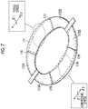
- Fig. 7 schematically illustrates the distribution of the directions of the principal stresses in the piezoelectric bodies of the first actuator part 30 and the second actuator part 40 during the resonance driving illustrated in Fig. 6 .
- first actuator part 30 and the second actuator part 40 are in the bending deformation state illustrated in Figs. 6 and 7 in a state of being driven by the resonance mode vibration
- portions to which stress in a tensile direction (tensile stress) is applied, and portions (reference numerals 172A, 172B, and 174 in Fig. 7 ) to which stress in a compressive direction (compressive stress) is applied occur (see Fig. 6 ).
- the upper electrodes are divided so as to correspond to the division of the piezoelectric body regions in which stresses in opposite directions are generated, and each of the electrode parts (51, 63A, 63B, 52A, 52B, and 64) is disposed.
- the “compressive stress” and the “tensile stress” mentioned here are defined by selecting two principal stresses in a plane substantially orthogonal to the film thickness direction of the piezoelectric body 166 from three orthogonal principal stress vectors and determining the direction with a higher absolute value (the direction with the maximum principal stress).
- the two principal stresses in the plane substantially orthogonal to the film thickness direction are stresses generated in the x-y plane, and correspond to ⁇ 1 and ⁇ 2 in Fig. 7 .
- the direction with the highest component absolute value is the direction of ⁇ 2 in Fig. 7 .
- a vector in a direction toward the outside is defined as the tensile direction
- a vector in a direction toward the inside is defined as the compressive direction.
- the dimensions of the actuator part are generally planar in the piezoelectric MEMS device and the stress ⁇ 3 in the film thickness direction can be regarded as almost 0.
- the phrase "the dimensions are planar” means that the height is sufficiently smaller than the dimension in the plane direction.
- the term “stresses in opposite directions” is determined on the basis of the above definition.
- the plane direction of the "x-y plane” described above corresponds to the "in-plane direction orthogonal to the film thickness direction of the piezoelectric body".
- the first piezoelectric conversion part 81, the second piezoelectric conversion parts 82A and 82B, the third piezoelectric conversion parts 103A and 103B, and the fourth piezoelectric conversion part 104 are disposed so as to correspond to the division of the regions (reference numerals 171, 172A, 172B, 173A, 173B, and 174) of the piezoelectric parts having different stress directions.
- the first piezoelectric conversion part 81 is provided for the tensile stress region 171 in Fig. 7
- the second piezoelectric conversion part 82A is provided for the compressive stress region 172A
- the second piezoelectric conversion part 82B is provided for the compressive stress region 172B
- the third piezoelectric conversion part 103A is provided for the tensile stress region 173A
- the third piezoelectric conversion part 103B is provided for the tensile stress region 173B
- the fourth piezoelectric conversion part 104 Is provided for the compressive stress region 174.
- the insulating parts 55, 57, 65, and 67 are formed to respectively correspond to the intermediate regions 176, 177, 178, and 179.
- the stress distribution during an operation due to resonance mode vibration can be analyzed by using a mode analysis method with parameters such as device dimensions, the Young's modulus of a material, and device shapes, which are given by using a well-known finite element method software.
- the stress distribution in the piezoelectric body at the time of driving in the resonance mode is analyzed, the regions of the piezoelectric conversion parts are divided so as to correspond to the division of the compressive stress regions and the tensile stress regions in the stress distribution on the basis of the analysis result, and the arrangement of the first piezoelectric conversion part 81, the second piezoelectric conversion parts 82A and 82B, the third piezoelectric conversion parts 103A and 103B, and the fourth piezoelectric conversion part 104 is determined.
- the piezoelectric conversion parts can be divided into two groups.
- the first piezoelectric conversion part 81 and the third piezoelectric conversion parts 103A and 103B belong to a first group (first electrode group)
- the second piezoelectric conversion parts 82A and 82B and the fourth piezoelectric conversion part 104 belong to a second group (second electrode group).
- any one electrode part of the upper electrode part and the lower electrode part of the piezoelectric conversion parts (piezoelectric conversion parts belonging to the same group) corresponding to the region with the same stress direction are set to be at the ground potential, and the in-phase drive voltage is applied the other electrode part.
- the pressure conversion parts piezoelectric conversion part belonging to different groups corresponding to the region of different stress directions (stresses in opposite directions) are configured so that the lower electrode of the piezoelectric conversion part belonging to one group is set to be at the ground potential and the voltage waveform V 1 is applied to the upper electrode while the upper electrode of the piezoelectric conversion part belonging to the other group is set to be at the ground potential and the voltage waveform V 2 in phase with V 1 is applied to the lower electrode. Accordingly, in the most efficient manner, a piezoelectric force can be converted into tilt displacement.
- the piezoelectric can be converted into displacement in the most efficient manner.
- the piezoelectric can be also converted into displacement in the most efficient manner.
- the example in which the voltage waveform V 1 is applied to the first upper electrode part 51 and the third upper electrode parts 63A and 63B and the voltage waveform V 2 is applied to the second lower electrode parts 72A and 72B and the fourth lower electrode part 94 is illustrated.
- the voltage waveform V 2 may also applied to the first upper electrode part 51 and the third upper electrode parts 63A and 63B and the voltage waveform V 1 may also be applied to the second lower electrode parts 72A and 72B and the fourth lower electrode part 94.
- first upper electrode part 51 and the third upper electrode parts 63A, 63B are set to be at the ground potential and the voltage waveform V 1 of the drive voltage is applied to the first lower electrode part 71 and the third lower electrode parts 93A and 93B while the second lower electrode parts 72A and 72B and the fourth lower electrode part 94 are set to be at the ground potential and the voltage waveform V 2 of the drive voltage is applied to the second upper electrode parts 52A and 52B and the fourth upper electrode part 64 is also possible.
- the electrode parts having the same potential are connected by wiring parts.
- the fourth piezoelectric conversion part 104 are used as driving force generating parts
- an embodiment in which some piezoelectric conversion parts thereof are used as sensor parts (stress detection part) for sensing (for detection) is also possible.
- each of the electrode parts constituting the electrode pair of each piezoelectric conversion part is not limited to an embodiment constituted by a single electrode, and at least one electrode part among the electrode parts (51, 52A, 52B, 63A, 63B, 64, 71, 72A, 72B, 93A, 93B, and 94) may also be constituted by a plurality of electrodes.
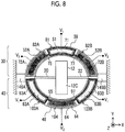
- Fig. 8 shows an example in which all electrode parts of the first piezoelectric conversion part 81, the second piezoelectric conversion parts 82A and 82B, the third piezoelectric conversion parts 103A and 103B, and the fourth piezoelectric conversion part 104 are used as electrodes for driving.
- Portions of each of the electrode parts (51, 52A, 52B, 63A, 63B, and 64) as the upper electrodes 168 and each of the electrode parts (71, 72A, 72B, 93A, 93B, and 94) as the lower electrodes 164 with the piezoelectric body 166 interposed therebetween each operate as a piezoelectric conversion part.
- all the electrode parts are used as the electrodes for driving (driving electrodes), and all the piezoelectric conversion parts function as driving force generating parts.
- an upper electrode driving system which performs piezoelectric driving by connecting each of the lower electrode parts (71, 93A, and 93B) to the ground potential, and applying the voltage waveform V1 as the drive voltage to the upper electrode parts (51, 63A, and 63B) is employed.
- a lower electrode driving system which is driven by connecting each of the upper electrode parts (52A, 52B, and 64) to the ground potential and applying the voltage waveform V 2 in phase with V 1 to the lower electrode parts (72A, 72B, and 94) is employed.
- phase is not limited to a phase difference of 0° and includes an allowable range of a phase difference (for example, ⁇ 10°) that can be substantially treated as the same phase to a degree at which no problems are caused in practice.
- the voltage amplitude and the phase difference of the drive voltage applied to each piezoelectric element part may be appropriately adjusted.
- a case of changing the voltage amplitude and the phase difference within the range of such adjustment is also included in the scope of the implementation of the present invention.
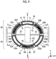
- Fig. 9 shows an example in which some electrode parts of the first piezoelectric conversion part 81, the second piezoelectric conversion parts 82A and 82B, the third piezoelectric conversion parts 103A and 103B, and the fourth piezoelectric conversion part 104 are used to sensing (detection) electrodes for stress detection.
- the fourth piezoelectric conversion part 104 when an electrically open state (that is, synonymous with "open state") is set between the upper electrode the lower electrode as an electrode pair, stress during driving can be detected by detecting a potential difference generated by a positive piezoelectric effect of the piezoelectric body 166.
- an electrically open state that is, synonymous with "open state”
- FIG. 9 an example in which the second piezoelectric conversion parts 82A and 82B and the third piezoelectric conversion parts 103A and 103B are used as sensor parts, the second lower electrode parts 72A and 72B and the third upper electrode parts 63A and 63B are used as detection electrodes, and the other piezoelectric conversion parts are used as driving force generating parts is illustrated.
- the detection electrode is set to be at a floating potential, and detects a voltage generated by the piezoelectric effect (positive piezoelectric effect) of the piezoelectric body 166.
- the electrodes indicated by “s 1 " and “s 2 " are detection electrodes for extracting a signal for sensing and represent electrodes set to be at a floating potential. Setting at the floating potential is synonymous with setting to the electrically open state.
- a voltage generated by the positive piezoelectric effect of the piezoelectric body can be detected, and from the detected voltage signal (detection signal), the stress of the actuator part can be detected. That is, the voltage detection part functions as a stress detection part. Accordingly, a feedback driving circuit that monitors the driven state of the mirror part 12 during driving of the mirror part 12 and enables the resonance state to be maintained or the like can be configured.
- At least one voltage detection part is provided for each of the actuator parts (30 and 40) constituting the piezoelectric actuator part 16. As described above, by providing the voltage detection part for each of the actuator parts, the operation state of each of the actuator parts can be recognized. Therefore, control on the application of an appropriate drive voltage based on the detection signal can be achieved, and more stable resonance driving can be realized.
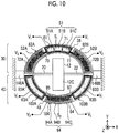
- Fig. 10 shows an example in which each of the first upper electrode part 51 and the fourth lower electrode part 94 described with reference to Fig. 8 is further divided into a plurality of electrodes.
- Fig. 10 an example in which the first upper electrode part 51 is divided into three electrodes 51 A, 51B, and 51C in the length direction of the first actuator part 30, and the fourth lower electrode part 94 is divided into three electrodes 94A, 94B, and 94C in the length direction of the second actuator part 40 is illustrated.
- Each of the first lower electrode part 71 and the fourth upper electrode part 64 is constituted by a single electrode.
- the first lower electrode part 71 and the fourth upper electrode part 64 may also be divided into a plurality of electrodes according to the arrangement of the electrodes 51 A, 51B, and 51C of the first upper electrode part 51 and the electrodes 94A, 94B, and 94C of the fourth lower electrode part 94.
- the electrode 51B disposed at the center is used as a voltage detection part (electrode for sensing) at a floating potential, and the remaining (left and right) electrodes 51A and 51C are used as drive voltage application parts (that is, driving force generating parts).
- the electrode 94B disposed at the center is used as a voltage detection part (electrode for sensing) at a floating potential and the remaining (left and right) electrodes 94A and 94C are used as drive voltage application parts (that is, driving force generating parts). Accordingly, stress detection can be achieved while minimizing the electrode region occupied by the voltage detection parts and maintaining a high scan angle.
- a form in which each of the first upper electrode part 51 and the fourth lower electrode part 94 is further divided is illustrated.
- a form in which the second lower electrode parts 72A and 72B or the third upper electrode parts 63A and 63B are further divided into a plurality of electrodes is also possible.
- stress detection can be achieved while minimizing portions occupied by stress detection and maintaining a high scan angle.
- Example 1 a micromirror device was fabricated by the following production method.
- a silicon on insulator (SOI) substrate having a laminated structure of a handle layer of 350 micrometers [ ⁇ m], a box layer of 1 micrometer [ ⁇ m], and a device layer of 24 micrometers [ ⁇ m], a Ti layer of 30 nanometers [nm] and an Ir layer of 150 nanometers [nm] were formed at a substrate temperature of 350°C by a sputtering method.
- a conductive layer formed by the laminate of the Ti layer (30 nm) and the Ir layer (150 nm) corresponds to the "lower electrode 164" described with reference to Fig. 4 .
- a piezoelectric body (PZT) layer was formed into 2.5 micrometers [ ⁇ m] on the substrate in which the laminate of the lower electrode (Ti / Ir) was formed in Procedure 1, by sing a radio frequency (RF) sputtering device.
- RF radio frequency
- a mixed gas of 97.5% Ar and 2.5% O 2 was used as the film formation gas, and a target material having a composition of Pb 1.3 ((Zr 0.52 Ti 0.48 ) 0.88 Nb 0.12 )O 3 was used.
- the film formation pressure was set to 2.2 millitorr [mTorr] (about 0.293 pascal [Pa]), and the film formation temperature was set to 450°C.
- the obtained PZT layer was an Nb-doped PZT thin film to which Nb was added in an atomic compositional ratio of 12%.
- the ratio of the amount "a" of Pb contained in the PZT thin film having a perovskite structure that is actually obtained can take a value other than "1.00" due to the presence of interstitial atoms, defects, and the like.
- the ratio c of O atoms can also take a value other than "3.00".
- a desired pattern may be formed in the lower electrode forming process of Procedure 1, and a desired pattern may be formed by etching in Procedure 3.
- the PZT thin film was directly formed on the substrate by the sputtering method, and the dry etching was thereafter performed.
- the fabrication process can be simplified and fine patterning can be achieved. Accordingly, the yield can be significantly improved, a further reduction in the size of the device can be coped with.
- the piezoelectric body of the actuator part is not limited to the thin film piezoelectric body, and a unimorph actuator may also be formed by attaching a bulk piezoelectric body to a vibration plate.
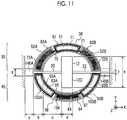
- Fig. 11 As an example of the shape of the device according to Example 1, specific examples of dimensions of Example 1 are illustrated in Fig. 11 .
- a 0.05 mm
- b 1.0 mm
- c 4.0 mm
- d 1.32 mm
- e 2.96 mm
- f 0.08 mm
- the resonance frequency of a resonance mode used for scanning is around 3350 Hz.
- the dimension a is the length in the x-axis direction of the base end parts (164A and 164B).
- the dimension b is the width dimension in the x-axis direction of the beam (beam) portions in the actuator parts (30 and 40).
- the dimension c is the length in the x-axis direction of the torsion bar parts (20 and 22).
- the dimension d is the width dimension in the x-axis direction of the mirror part 12.
- the dimension e is the length of the mirror part 12 in the y-axis direction.
- the dimension f is the width dimension in the y-axis direction of the torsion bar parts (20 and 22).
- the dimension g is the width dimension in the y-axis direction of the base end parts (164A and 164B).
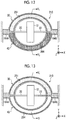
- a micromirror device according to Comparative Example 1 as illustrated in Fig. 12 was fabricated using exactly the same substrate (SOI substrate) and production process method as those in Example 1.
- the device 210 illustrated in Fig. 12 like elements that are the same as or similar to those described with reference to Fig. 3 are denoted by like reference numerals, and description thereof will be omitted.
- the device 210 of Comparative Example 1 illustrated in Fig. 12 has a structure in which the upper electrodes of the first actuator part 30 and the second actuator part 40 have only a single electrode part 251 and a single electrode part 264, respectively.
- the lower electrode of the device 210 is not divided and is a single (solid) common electrode.
- Fig. 12 shows an example in which these two electrode parts 251 and 264 are used as electrodes for driving.
- a voltage waveform V 1 may be applied to the electrode part 251 of the first actuator part 30, and a voltage waveform V 3 which is in antiphase with V 1 may be applied to the electrode part 264 of the second actuator part 40.
- V 3 the following waveform may be used.
- V 3 V off 3 + V 3 A sin ⁇ t + ⁇
- V off3 is the offset voltage
- V 3A is the voltage amplitude
- ⁇ is the phase difference
- ⁇ 180° is given herein.
- any one electrode part of the two electrode parts 251 and 264 is used for detection (sensing).
- Fig. 13 shows an example in which the electrode part 264 of the second actuator part 40 is used for sensing.
- the electrode part 264 used for sensing is set to be at a floating potential and detects a voltage generated by a positive piezoelectric effect of the piezoelectric body.
- the electrode indicated by "s" is a detection electrode for extracting a signal for sensing and represents an electrode set to be at a floating potential.
- Fig. 14 is a graph showing the relationship between the drive voltage and the scan angle in the device as an experiment subject.
- the voltage waveforms V 1 and V 2 in a sine wave having a voltage amplitude V PP are input to the electrode parts for driving in each device to induce resonance vibration accompanied with the rotational motion of the mirror part 12, and the mechanical deflection angle of the mirror part 12 was measured at a laser scan angle.
- the devices of “Example 1” and “Example 1 (with angle sensing)” conform to the illustration of Figs. 8 and 9 , respectively.
- the devices of "Comparative Example 1 (driving only)” and “Comparative Example 1 (with angle sensing)” conform to the illustration of Figs. 12 and 13 , respectively.
- Fig. 14 The results of the experiment are shown in Fig. 14 .
- the horizontal axis represents the voltage amplitude (in units of volts [V]), and the vertical axis represents the optical scan angle (in units of degrees [deg]).
- the device of Example 1 including a plurality of electrode parts in a single actuator part has a higher scan angle than that of the device of Comparative Example 1.
- the device of Example 1 can maintain a higher scan angle than that of the device of Comparative Example 1.
- a piezoelectric body suitable for this embodiment may be a body including one or two or more perovskite type oxides represented by the following general formula (P-1).
- P-1 General formula ABO 3 ...
- P-1 In the formula, A is an element in A-site and is at least one element including Pb.
- the molar ratio between the A-site element, the B-site element, and the oxygen element is 1 : 1 : 3 as a standard, and the molar ratio may also be deviated from the reference molar ratio within a range in which the perovskite structure can be achieved.
- the perovskite type oxides represented by the above general formula (P-1) include: lead-containing compounds such as lead titanate, lead zirconate titanate (PZT), lead zirconate, lanthanum lead titanate, lead lanthanum zirconate titanate, lead magnesium niobate-lead zirconate titanate, lead nickel niobate-lead zirconate titanate, and lead zinc niobate-lead zirconate titanate and mixed crystal systems thereof; and lead-free compounds such as barium titanate, strontium barium titanate, sodium bismuth titanate, bismuth potassium titanate, sodium niobate, potassium niobate, lithium niobate, and bismuth ferrite and mixed crystal systems thereof.
- lead-containing compounds such as lead titanate, lead zirconate titanate (PZT), lead zirconate, lanthanum lead titanate, lead lanthanum zirconate titanate, lead
- the piezoelectric film of this embodiment preferably includes one or two or more perovskite type oxides (P-2) represented by the following general formula (P-2).
- P-2 perovskite type oxides
- General formula A a (Zr x ,Ti y ,M b-x-y ) b O c ...
- P-2 perovskite type oxides
- the perovskite type oxide is an oxide in which a part of the B-site of intrinsic PZT or PZT is substituted with M. It is known that in the PZT to which various donor ions having a valence higher than the valence of the substituted ion are added, characteristics such as piezoelectric performance are improved compared to the intrinsic PZT. It is preferable that M is one or two or more donor ions having a valence higher than that of tetravalent Zr or Ti. As such donor ions, there are V 5+ , Nb 5+ , Ta 5+ , Sb 5+ , Mo 6+ , and W 6+ .
- the range of b-x-y is not particularly limited as long as the perovskite structure can be achieved.
- the molar ratio Nb / (Zr + Ti + Nb) is preferably 0.05 or more and 0.25 or less, and more preferably 0.06 or more and 0.20 or less.
- a piezoelectric actuator comprising the piezoelectric film has excellent displacement characteristics.
- the piezoelectric actuator comprising the piezoelectric film made of the perovskite type oxides represented by the general formulas (P-1) and (P-2) has voltage-displacement characteristics with excellent linearity. These piezoelectric materials exhibit good actuator characteristics and sensor characteristics when the present invention is implemented.
- the perovskite type oxide represented by the general formula (P-2) has a higher piezoelectric constant than that represented by the general formula (P-1).
- a lead zirconate titanate (PZT) thin film doped with Nb in an atomic composition percentage of 12% may be used.
- PZT lead zirconate titanate
- PZT is selected as the piezoelectric material used for the actuator part (the driving force generating part and the stress detection part), but the piezoelectric material does not need to be limited to this material.
- a lead-free piezoelectric body such as BaTiO 3 , KNaNbO 3 , or BiFeO 3 may be used, and a non-perovskite piezoelectric body such as AlN and ZnO 2 may also be used.
- a vapor deposition method is preferable as the film formation method of the piezoelectric body.
- various methods such as an ion plating method, a metal organic chemical vapor deposition (MOCVD) method, and a pulse laser deposition (PLD) method may be applied.
- MOCVD metal organic chemical vapor deposition
- PLD pulse laser deposition
- a method other than the vapor deposition method for example, sol-gel method.
- a configuration in which a piezoelectric thin film is directly formed on a substrate by a vapor deposition method or a sol-gel method is preferable.
- the piezoelectric body 166 of this embodiment is preferably a thin film having a film thickness of 1 ⁇ m or more and 10 ⁇ m or less.
- Example 1 voltage waveforms which are in phase are used as the waveforms of the drive voltages.
- the phases of the two do not need to be completely coincident with each other, and the phase difference therebetween may be shifted to some extent from 0°.
- the phase difference between V 1 and V 2 is shifted from 0° by a small amount from in order to eliminate this component.
- the waveforms can be regarded as being in phase.
- the voltage amplitudes V 1A and V 2A of the voltage waveforms may be different from each other or may be any value including 0 V.
- the application voltage is not limited to a sine wave, and periodic waveforms such as a square wave and a triangular wave may also be applied thereto.
- the types of the drive waveforms may be two or more types.
- the voltage waveform applied to the first upper electrode part 51 may be set to V 11
- the voltage waveform applied to the second lower electrode parts 72A and 72B may be set to V 12
- the voltage waveform applied to the third upper electrode parts 63A and 63B may be set to V 21
- the voltage waveform applied to the fourth lower electrode part 94 may be set to V 22 .
- V 11 V off 11 + V 11 A sin ⁇ t
- V 12 V off 12 + V 12 A sin ⁇ t
- V 12 V off 21 + V 21 A sin ⁇ t
- V 22 V off 22 + V 22 A sin ⁇ t
- each of V 11A , V 12A , V 21A , and V 22A is the voltage amplitude, ⁇ is the angular frequency, and t is the time.
- Each of V 11A , V 12A , V 21A , and V 22A may have an arbitrary value of 0 or more. All of V 11A , V 12A , V 21A , and V 22A may be set to different values, or some or all thereof may also be set to the same value.
- the phases of V 11 and V 21 are coincident with each other, and the phases of V 12 and V 22 are coincident with each other. However, these phases do not need to be completely coincident with each other, and a slight phase shift of about ⁇ 10° is acceptable.
- Fig. 16 is a diagram illustrating an example of the configuration of a control system used for driving a device.
- the control system of the device form described with reference to Fig. 10 is illustrated.
- the electrodes 51A and 51C in the first upper electrode part 51 and the second lower electrode parts 72A and 72B in the first actuator part 30 used for driving, and the third upper electrode parts 63A and 63B and the electrodes 94A and 94C of and the fourth lower electrode part 94 in the second actuator part 40 are connected to the corresponding voltage output terminals of a driving circuit 310.
- the voltage waveform V 1 for driving is supplied from the driving circuit 310 to the electrodes 51A and 51C of the first actuator part 30 and the third upper electrode parts 63A and 63B of the second actuator part 40.
- the voltage waveform V 2 for driving is supplied from the driving circuit 310 to the second lower electrode parts 72A and 72B of the first actuator part 30 and the electrodes 94A and 94C of the second actuator part 40.
- the electrode parts to which the same drive voltage is applied are connected in parallel, a configuration in which drive voltages are individually supplied to the electrode parts may also be employed.
- the driving circuit 310 supplies the voltage waveforms V 1 and V 2 of the drive voltage for causing the mirror part 12 to undergo resonance driving at near the resonance frequency fx of the resonance mode in which the mirror part 12 (see Fig. 3 ) performs rotational motion about the rotation axis R A .
- the displacement amount reaches the highest value when the frequency of the drive voltage is caused to be completely coincident with the resonance frequency of the device.
- the displacement amount greatly decreases when the resonance frequency slightly changes due to the influence of temperature and the like.
- driving is performed at a frequency slightly shifted from the resonance frequency within a range where a necessary displacement amount can be secured.
- Near the resonance frequency fx has a meaning including a frequency coincident with the resonance frequency fx and a frequency slightly shifted from the resonance frequency fx within a range in which a necessary displacement amount can be secured.
- Each of the electrode 51B of the first actuator part 30 and the electrode 94B of the second actuator part 40, which are used for sensing, is connected to a detection circuit 312.
- the first lower electrode part 71 and the second upper electrode parts 52A and 52B in the first actuator part 30 and the third lower electrode parts 93A and 93B and the fourth upper electrode part 64 in the second actuator part 40 are connected to the common terminal (V 0 terminal, for example, GND terminal) of the driving circuit 310 or the detection circuit 312.
- Each electrode is connected to the driving circuit 310 or the detection circuit 312 via a wiring member such as wire bonding or a pattern wiring part on a substrate (not illustrated).
- a voltage signal is detected from the electrode 51B and the electrode 94B for sensing via the detection circuit 312, and the detection results are notified to a control circuit 314.
- the control circuit 314 sends a control signal to the driving circuit 310 so as to maintain resonance and controls the application of the drive voltages to the first actuator part 30 and the second actuator part 40.
- feedback is applied to the driving circuit 310 so as to maintain resonance so that the phases of the waveform of the drive voltage applied to the piezoelectric actuator parts and the waveform detected from the stress detection part (sensor part) have predetermined values.
- the control circuit 314 controls the voltage or driving frequency applied to the piezoelectric actuator part based on the detection signal obtained from the stress detection part of the mirror part 12.
- Such a feedback control circuit may be embedded in the detection circuit 312.
- the driving circuit 310, the detection circuit 312, and the control circuit 314 may be collectively configured as an integrated circuit such as an application specific integrated circuit (ASIC).
- ASIC application specific integrated circuit
- the electrode parts are arranged according to the stress distribution generated in the piezoelectric bodies at the time of deformation of the actuator parts, the actuator parts can be efficiently driven, and compared to the configuration in the related art, a larger mirror tilt angle can be obtained.
- the displacement efficiency is improved compared to the configuration in the related art, even in a case where some of the electrodes are used for stress detection, a sufficient displacement angle can be obtained.
- driving can be performed by using voltage waveforms which are in phase, the configuration of the driving circuit can be simplified. In particular, as the simplest configuration, a configuration in which the first actuator part 30 and the second actuator part 40 are displaced in opposite directions by one type of voltage waveform.
- Fig. 17 is a plan view illustrating the configuration of main parts of a micromirror device according to a third embodiment.
- a micromirror device 410 illustrated in Fig. 17 like elements that are the same as or similar to those described with reference to Fig. 1 are denoted by like reference numerals, and description thereof will be omitted.
- illustration of the fixing frame 18 is omitted.
- the micromirror device 410 corresponds to a form of "mirror driving device".
- the movable part 38 that connects the first base end parts 36A and 36B, which are end parts on both sides in the x-axis direction has a shape along three sides corresponding to the upper base and the two legs of a substantially isosceles trapezoid.
- the movable part 48 that connects the second base end parts 46A and 46B, which are end parts on both sides in the x-axis direction has a shape along three sides corresponding to the upper base and the two legs of a substantially isosceles trapezoid.
- the first actuator part 30 and the second actuator part 40 having the actuator shape as illustrated in Fig. 17 may be employed.
- the actuator shapes of the first actuator part 30 and the second actuator part 40 various forms are possible. As illustrated in Figs. 1 , 3 , and 17 , various forms of a configuration in which the movable part 38 that extends from the one first base end part 36A of the base end parts on both sides in the x-axis direction in the first actuator part 30 to the other first base end part 36B has a shape bypassing the mirror part 12, and the movable part 48 that extends from the one second base end part 46A of the base end parts on both sides in the x-axis direction in the second actuator part 40 to the other second base end part 46B has a shape bypassing the mirror part 12 can be designed.
- the first torsion bar part 20 and the second torsion bar part 22 are connected to positions coincident with the rotation axis R A of the mirror part 12, and are formed to extend in the axial direction of the rotation axis R A toward the outside of the mirror part 12.
- Fig. 3 illustrates an example in which the first torsion bar part 20 and the second torsion bar part 22 are connected to the positions coincident with the rotation axis R A of the mirror part 12.
- the connection positions of the torsion bar parts may not be strictly coincident with the rotation axis R A , and the torsion bar parts are not necessarily limited to a form of connection to a single point, and may be connected to a plurality of points.
- the substantially center portion in the longitudinal direction of the mirror part 12 (not limited to the true center point on design but the vicinity thereof) is the rotation axis R A
- a structure in which torsion bars are connected at positions of two or more points in axial symmetry with respect to the position of the rotation axis R A interposed therebetween within a range in which the position can be regarded as the substantially center portion is also possible.
- the mirror driving device of the present invention can be used in various applications as an optical device that reflects light such as laser light and changes the traveling direction of light.
- the mirror driving device can be widely applied to an optical deflector, an optical scanning device, a laser printer, a barcode reader, a display device, various optical sensors (distance measuring sensors and shape measurement sensors), an optical communication device, a laser projector, an optical coherence tomography diagnostic device, and the like.
- the present invention is not limited to the applications in which light is reflected, and can also be applied to a mirror device in applications in which sound waves are reflected.
Landscapes
- Physics & Mathematics (AREA)
- General Physics & Mathematics (AREA)
- Optics & Photonics (AREA)
- Chemical & Material Sciences (AREA)
- Engineering & Computer Science (AREA)
- Ceramic Engineering (AREA)
- Micromachines (AREA)
- Mechanical Optical Scanning Systems (AREA)
- Mechanical Light Control Or Optical Switches (AREA)
Applications Claiming Priority (2)
| Application Number | Priority Date | Filing Date | Title |
|---|---|---|---|
| JP2014201650 | 2014-09-30 | ||
| PCT/JP2015/077588 WO2016052547A1 (fr) | 2014-09-30 | 2015-09-29 | Dispositif d'entraînement de miroir et son procédé d'entraînement |
Publications (3)
| Publication Number | Publication Date |
|---|---|
| EP3203298A1 true EP3203298A1 (fr) | 2017-08-09 |
| EP3203298A4 EP3203298A4 (fr) | 2017-09-20 |
| EP3203298B1 EP3203298B1 (fr) | 2021-07-14 |
Family
ID=55630573
Family Applications (1)
| Application Number | Title | Priority Date | Filing Date |
|---|---|---|---|
| EP15847123.5A Active EP3203298B1 (fr) | 2014-09-30 | 2015-09-29 | Dispositif d'entraînement de miroir et son procédé d'entraînement |
Country Status (4)
| Country | Link |
|---|---|
| US (1) | US10371940B2 (fr) |
| EP (1) | EP3203298B1 (fr) |
| JP (1) | JP6308700B2 (fr) |
| WO (1) | WO2016052547A1 (fr) |
Families Citing this family (20)
| Publication number | Priority date | Publication date | Assignee | Title |
|---|---|---|---|---|
| DE112017000678B4 (de) * | 2016-02-05 | 2020-06-18 | Fujifilm Corporation | Piezoelektrisches Element |
| CN108604008B (zh) * | 2016-02-17 | 2020-11-10 | 三菱电机株式会社 | 反射镜驱动装置、反射镜驱动装置的控制方法及反射镜驱动装置的制造方法 |
| WO2018088291A1 (fr) * | 2016-11-09 | 2018-05-17 | 第一精工株式会社 | Élément réfléchissant mobile |
| US11262576B2 (en) * | 2017-10-31 | 2022-03-01 | Panasonic Intellectual Property Management Co., Ltd. | Reflective optical element |
| JP6985602B2 (ja) * | 2018-01-29 | 2021-12-22 | ミツミ電機株式会社 | 光走査装置及び光走査装置の製造方法 |
| JP7077682B2 (ja) | 2018-03-12 | 2022-05-31 | セイコーエプソン株式会社 | 圧電駆動装置、ロボット、電子部品搬送装置、プリンターおよびプロジェクター |
| JP6870699B2 (ja) * | 2018-05-03 | 2021-05-12 | 株式会社村田製作所 | 拡大された画像領域を備える走査光学デバイス |
| CN113574007B (zh) * | 2019-03-28 | 2024-12-03 | 富士胶片株式会社 | 微镜器件及微镜器件的驱动方法 |
| EP3961289A4 (fr) | 2019-04-26 | 2022-06-15 | FUJIFILM Corporation | Dispositif de micro-miroir |
| FI20196026A1 (en) | 2019-11-28 | 2021-05-29 | Teknologian Tutkimuskeskus Vtt Oy | Improvements for driving a microelectromechanical system mirror |
| US12514123B2 (en) | 2021-05-12 | 2025-12-30 | Hamamatsu Photonics K.K. | Actuator device and actuator system |
| JP7769558B2 (ja) | 2021-05-12 | 2025-11-13 | 浜松ホトニクス株式会社 | 圧電ユニット及びアクチュエータ装置 |
| US12527227B2 (en) * | 2021-05-12 | 2026-01-13 | Hamamatsu Photonics K.K. | Actuator device |
| JP7696305B2 (ja) | 2021-05-12 | 2025-06-20 | 浜松ホトニクス株式会社 | アクチュエータ装置 |
| DE102021134310B4 (de) | 2021-12-22 | 2025-12-24 | Tdk Electronics Ag | Piezoelektrisches Spiegelbauelement, Verfahren zum Betrieb des piezoelektrischen Spiegelbauelements und Projektionsvorrichtung mit dem piezoelektrischen Spiegelbauelement |
| CN119631004A (zh) * | 2022-07-25 | 2025-03-14 | 松下知识产权经营株式会社 | 驱动元件及光偏转元件 |
| DE102022209396A1 (de) * | 2022-09-09 | 2024-03-14 | Carl Zeiss Smt Gmbh | Verfahren zum Betreiben eines optischen Bauelements, optisches Bauelement |
| KR20250162805A (ko) | 2023-04-11 | 2025-11-19 | 티디케이 일렉트로닉스 아게 | 마이크로 전기 기계 미러, 마이크로 전기 기계 미러를 작동하기 위한 방법, 투사 장치 및 마이크로 전기 기계 미러의 용도 |
| DE102023109108B4 (de) * | 2023-04-11 | 2024-11-14 | Tdk Electronics Ag | Mikroelektromechanischer Spiegel, Verfahren zum Betrieb eines mikroelektromechanischen Spiegels, Projektionsvorrichtung und Verwendung eines mikroelektromechanischen Spiegels |
| DE102023005475B4 (de) * | 2023-04-11 | 2025-12-24 | Tdk Electronics Ag | Mikroelektromechanischer Spiegel, Verfahren zum Betrieb eines mikroelektromechanischen Spiegels, Projektionsvorrichtung und Verwendung eines mikroelektromechanischen Spiegels |
Family Cites Families (10)
| Publication number | Priority date | Publication date | Assignee | Title |
|---|---|---|---|---|
| JPH11112048A (ja) * | 1997-10-02 | 1999-04-23 | Seiko Epson Corp | 圧電体素子、インクジェット式記録ヘッドおよびそれらの製造方法 |
| JP2005128147A (ja) * | 2003-10-22 | 2005-05-19 | Stanley Electric Co Ltd | 光偏向器及び光学装置 |
| JP5055832B2 (ja) * | 2006-05-16 | 2012-10-24 | オムロン株式会社 | 駆動装置、光走査型装置及び物体情報検知装置 |
| JP4972781B2 (ja) | 2007-06-19 | 2012-07-11 | コニカミノルタアドバンストレイヤー株式会社 | マイクロスキャナ及びそれを備えた光走査装置。 |
| JP2010085506A (ja) | 2008-09-29 | 2010-04-15 | Brother Ind Ltd | 光スキャナ及びこの光スキャナを備えた画像表示装置 |
| JP5493735B2 (ja) * | 2009-01-30 | 2014-05-14 | 株式会社リコー | 偏向ミラー、光走査装置、画像形成装置、および画像投影装置 |
| US9158108B2 (en) * | 2010-07-29 | 2015-10-13 | Nec Corporation | Optical scanning device and image display device |
| JP5264954B2 (ja) | 2011-03-30 | 2013-08-14 | 富士フイルム株式会社 | ミラー駆動装置及び方法 |
| JP5943870B2 (ja) * | 2013-04-01 | 2016-07-05 | 富士フイルム株式会社 | 圧電体膜 |
| JP6092713B2 (ja) * | 2013-05-28 | 2017-03-08 | スタンレー電気株式会社 | 光偏向器 |
-
2015
- 2015-09-29 EP EP15847123.5A patent/EP3203298B1/fr active Active
- 2015-09-29 WO PCT/JP2015/077588 patent/WO2016052547A1/fr not_active Ceased
- 2015-09-29 JP JP2016552088A patent/JP6308700B2/ja active Active
-
2017
- 2017-03-29 US US15/473,129 patent/US10371940B2/en active Active
Also Published As
| Publication number | Publication date |
|---|---|
| EP3203298A4 (fr) | 2017-09-20 |
| EP3203298B1 (fr) | 2021-07-14 |
| WO2016052547A1 (fr) | 2016-04-07 |
| JP6308700B2 (ja) | 2018-04-11 |
| US20170199375A1 (en) | 2017-07-13 |
| US10371940B2 (en) | 2019-08-06 |
| JPWO2016052547A1 (ja) | 2017-09-07 |
Similar Documents
| Publication | Publication Date | Title |
|---|---|---|
| EP3203298B1 (fr) | Dispositif d'entraînement de miroir et son procédé d'entraînement | |
| EP3203297B1 (fr) | Dispositif d'entraînement de miroir et procédé d'entraînement pour celui-ci | |
| EP2827183B1 (fr) | Dispositif d'entraînement de miroir et son procédé de commande | |
| EP2827182B1 (fr) | Dispositif d'entraînement de miroir et son procédé de commande | |
| US10048489B2 (en) | Mirror driving device and driving method for same | |
| US12019235B2 (en) | Micromirror device and method of driving micromirror device | |
| JP5264954B2 (ja) | ミラー駆動装置及び方法 | |
| US8879132B2 (en) | Mirror driving apparatus, method of driving same and method of manufacturing same | |
| US20210405350A1 (en) | Micromirror device and method of driving micromirror device | |
| US20130208330A1 (en) | Mirror driving device and method of controlling the device | |
| JP7601961B2 (ja) | マイクロミラーデバイス | |
| EP3998505B1 (fr) | Dispositif à micromiroir |
Legal Events
| Date | Code | Title | Description |
|---|---|---|---|
| STAA | Information on the status of an ep patent application or granted ep patent |
Free format text: STATUS: THE INTERNATIONAL PUBLICATION HAS BEEN MADE |
|
| PUAI | Public reference made under article 153(3) epc to a published international application that has entered the european phase |
Free format text: ORIGINAL CODE: 0009012 |
|
| STAA | Information on the status of an ep patent application or granted ep patent |
Free format text: STATUS: REQUEST FOR EXAMINATION WAS MADE |
|
| 17P | Request for examination filed |
Effective date: 20170328 |
|
| AK | Designated contracting states |
Kind code of ref document: A1 Designated state(s): AL AT BE BG CH CY CZ DE DK EE ES FI FR GB GR HR HU IE IS IT LI LT LU LV MC MK MT NL NO PL PT RO RS SE SI SK SM TR |
|
| AX | Request for extension of the european patent |
Extension state: BA ME |
|
| A4 | Supplementary search report drawn up and despatched |
Effective date: 20170822 |
|
| RIC1 | Information provided on ipc code assigned before grant |
Ipc: H01L 41/09 20060101ALI20170816BHEP Ipc: H02N 2/00 20060101ALI20170816BHEP Ipc: G02B 26/08 20060101AFI20170816BHEP Ipc: H01L 41/04 20060101ALI20170816BHEP Ipc: H01L 41/187 20060101ALI20170816BHEP Ipc: G02B 26/10 20060101ALI20170816BHEP Ipc: B81B 3/00 20060101ALI20170816BHEP Ipc: H01L 41/113 20060101ALI20170816BHEP |
|
| DAV | Request for validation of the european patent (deleted) | ||
| DAX | Request for extension of the european patent (deleted) | ||
| GRAP | Despatch of communication of intention to grant a patent |
Free format text: ORIGINAL CODE: EPIDOSNIGR1 |
|
| STAA | Information on the status of an ep patent application or granted ep patent |
Free format text: STATUS: GRANT OF PATENT IS INTENDED |
|
| INTG | Intention to grant announced |
Effective date: 20200409 |
|
| GRAJ | Information related to disapproval of communication of intention to grant by the applicant or resumption of examination proceedings by the epo deleted |
Free format text: ORIGINAL CODE: EPIDOSDIGR1 |
|
| STAA | Information on the status of an ep patent application or granted ep patent |
Free format text: STATUS: REQUEST FOR EXAMINATION WAS MADE |
|
| STAA | Information on the status of an ep patent application or granted ep patent |
Free format text: STATUS: EXAMINATION IS IN PROGRESS |
|
| INTC | Intention to grant announced (deleted) | ||
| 17Q | First examination report despatched |
Effective date: 20200818 |
|
| GRAS | Grant fee paid |
Free format text: ORIGINAL CODE: EPIDOSNIGR3 |
|
| STAA | Information on the status of an ep patent application or granted ep patent |
Free format text: STATUS: GRANT OF PATENT IS INTENDED |
|
| GRAP | Despatch of communication of intention to grant a patent |
Free format text: ORIGINAL CODE: EPIDOSNIGR1 |
|
| RAP3 | Party data changed (applicant data changed or rights of an application transferred) |
Owner name: FUJIFILM CORPORATION |
|
| RIC1 | Information provided on ipc code assigned before grant |
Ipc: G02B 26/08 20060101AFI20210309BHEP Ipc: G02B 26/10 20060101ALI20210309BHEP Ipc: H01L 41/04 20060101ALN20210309BHEP Ipc: H01L 41/08 20060101ALN20210309BHEP Ipc: H01L 41/09 20060101ALN20210309BHEP Ipc: H01L 41/187 20060101ALN20210309BHEP |
|
| INTG | Intention to grant announced |
Effective date: 20210324 |
|
| GRAF | Information related to payment of grant fee modified |
Free format text: ORIGINAL CODE: EPIDOSCIGR3 |
|
| GRAA | (expected) grant |
Free format text: ORIGINAL CODE: 0009210 |
|
| STAA | Information on the status of an ep patent application or granted ep patent |
Free format text: STATUS: THE PATENT HAS BEEN GRANTED |
|
| AK | Designated contracting states |
Kind code of ref document: B1 Designated state(s): AL AT BE BG CH CY CZ DE DK EE ES FI FR GB GR HR HU IE IS IT LI LT LU LV MC MK MT NL NO PL PT RO RS SE SI SK SM TR |
|
| REG | Reference to a national code |
Ref country code: GB Ref legal event code: FG4D |
|
| REG | Reference to a national code |
Ref country code: IE Ref legal event code: FG4D |
|
| REG | Reference to a national code |
Ref country code: DE Ref legal event code: R096 Ref document number: 602015071365 Country of ref document: DE |
|
| REG | Reference to a national code |
Ref country code: AT Ref legal event code: REF Ref document number: 1411116 Country of ref document: AT Kind code of ref document: T Effective date: 20210815 |
|
| REG | Reference to a national code |
Ref country code: LT Ref legal event code: MG9D |
|
| REG | Reference to a national code |
Ref country code: NL Ref legal event code: MP Effective date: 20210714 |
|
| REG | Reference to a national code |
Ref country code: AT Ref legal event code: MK05 Ref document number: 1411116 Country of ref document: AT Kind code of ref document: T Effective date: 20210714 |
|
| PG25 | Lapsed in a contracting state [announced via postgrant information from national office to epo] |
Ref country code: SE Free format text: LAPSE BECAUSE OF FAILURE TO SUBMIT A TRANSLATION OF THE DESCRIPTION OR TO PAY THE FEE WITHIN THE PRESCRIBED TIME-LIMIT Effective date: 20210714 Ref country code: RS Free format text: LAPSE BECAUSE OF FAILURE TO SUBMIT A TRANSLATION OF THE DESCRIPTION OR TO PAY THE FEE WITHIN THE PRESCRIBED TIME-LIMIT Effective date: 20210714 Ref country code: HR Free format text: LAPSE BECAUSE OF FAILURE TO SUBMIT A TRANSLATION OF THE DESCRIPTION OR TO PAY THE FEE WITHIN THE PRESCRIBED TIME-LIMIT Effective date: 20210714 Ref country code: AT Free format text: LAPSE BECAUSE OF FAILURE TO SUBMIT A TRANSLATION OF THE DESCRIPTION OR TO PAY THE FEE WITHIN THE PRESCRIBED TIME-LIMIT Effective date: 20210714 Ref country code: BG Free format text: LAPSE BECAUSE OF FAILURE TO SUBMIT A TRANSLATION OF THE DESCRIPTION OR TO PAY THE FEE WITHIN THE PRESCRIBED TIME-LIMIT Effective date: 20211014 Ref country code: LT Free format text: LAPSE BECAUSE OF FAILURE TO SUBMIT A TRANSLATION OF THE DESCRIPTION OR TO PAY THE FEE WITHIN THE PRESCRIBED TIME-LIMIT Effective date: 20210714 Ref country code: PT Free format text: LAPSE BECAUSE OF FAILURE TO SUBMIT A TRANSLATION OF THE DESCRIPTION OR TO PAY THE FEE WITHIN THE PRESCRIBED TIME-LIMIT Effective date: 20211115 Ref country code: NO Free format text: LAPSE BECAUSE OF FAILURE TO SUBMIT A TRANSLATION OF THE DESCRIPTION OR TO PAY THE FEE WITHIN THE PRESCRIBED TIME-LIMIT Effective date: 20211014 Ref country code: NL Free format text: LAPSE BECAUSE OF FAILURE TO SUBMIT A TRANSLATION OF THE DESCRIPTION OR TO PAY THE FEE WITHIN THE PRESCRIBED TIME-LIMIT Effective date: 20210714 Ref country code: FI Free format text: LAPSE BECAUSE OF FAILURE TO SUBMIT A TRANSLATION OF THE DESCRIPTION OR TO PAY THE FEE WITHIN THE PRESCRIBED TIME-LIMIT Effective date: 20210714 Ref country code: ES Free format text: LAPSE BECAUSE OF FAILURE TO SUBMIT A TRANSLATION OF THE DESCRIPTION OR TO PAY THE FEE WITHIN THE PRESCRIBED TIME-LIMIT Effective date: 20210714 |
|
| PG25 | Lapsed in a contracting state [announced via postgrant information from national office to epo] |
Ref country code: PL Free format text: LAPSE BECAUSE OF FAILURE TO SUBMIT A TRANSLATION OF THE DESCRIPTION OR TO PAY THE FEE WITHIN THE PRESCRIBED TIME-LIMIT Effective date: 20210714 Ref country code: LV Free format text: LAPSE BECAUSE OF FAILURE TO SUBMIT A TRANSLATION OF THE DESCRIPTION OR TO PAY THE FEE WITHIN THE PRESCRIBED TIME-LIMIT Effective date: 20210714 Ref country code: GR Free format text: LAPSE BECAUSE OF FAILURE TO SUBMIT A TRANSLATION OF THE DESCRIPTION OR TO PAY THE FEE WITHIN THE PRESCRIBED TIME-LIMIT Effective date: 20211015 |
|
| REG | Reference to a national code |
Ref country code: DE Ref legal event code: R097 Ref document number: 602015071365 Country of ref document: DE |
|
| PG25 | Lapsed in a contracting state [announced via postgrant information from national office to epo] |
Ref country code: DK Free format text: LAPSE BECAUSE OF FAILURE TO SUBMIT A TRANSLATION OF THE DESCRIPTION OR TO PAY THE FEE WITHIN THE PRESCRIBED TIME-LIMIT Effective date: 20210714 |
|
| REG | Reference to a national code |
Ref country code: CH Ref legal event code: PL |
|
| PLBE | No opposition filed within time limit |
Free format text: ORIGINAL CODE: 0009261 |
|
| REG | Reference to a national code |
Ref country code: BE Ref legal event code: MM Effective date: 20210930 |
|
| STAA | Information on the status of an ep patent application or granted ep patent |
Free format text: STATUS: NO OPPOSITION FILED WITHIN TIME LIMIT |
|
| PG25 | Lapsed in a contracting state [announced via postgrant information from national office to epo] |
Ref country code: SM Free format text: LAPSE BECAUSE OF FAILURE TO SUBMIT A TRANSLATION OF THE DESCRIPTION OR TO PAY THE FEE WITHIN THE PRESCRIBED TIME-LIMIT Effective date: 20210714 Ref country code: SK Free format text: LAPSE BECAUSE OF FAILURE TO SUBMIT A TRANSLATION OF THE DESCRIPTION OR TO PAY THE FEE WITHIN THE PRESCRIBED TIME-LIMIT Effective date: 20210714 Ref country code: RO Free format text: LAPSE BECAUSE OF FAILURE TO SUBMIT A TRANSLATION OF THE DESCRIPTION OR TO PAY THE FEE WITHIN THE PRESCRIBED TIME-LIMIT Effective date: 20210714 Ref country code: MC Free format text: LAPSE BECAUSE OF FAILURE TO SUBMIT A TRANSLATION OF THE DESCRIPTION OR TO PAY THE FEE WITHIN THE PRESCRIBED TIME-LIMIT Effective date: 20210714 Ref country code: EE Free format text: LAPSE BECAUSE OF FAILURE TO SUBMIT A TRANSLATION OF THE DESCRIPTION OR TO PAY THE FEE WITHIN THE PRESCRIBED TIME-LIMIT Effective date: 20210714 Ref country code: CZ Free format text: LAPSE BECAUSE OF FAILURE TO SUBMIT A TRANSLATION OF THE DESCRIPTION OR TO PAY THE FEE WITHIN THE PRESCRIBED TIME-LIMIT Effective date: 20210714 Ref country code: AL Free format text: LAPSE BECAUSE OF FAILURE TO SUBMIT A TRANSLATION OF THE DESCRIPTION OR TO PAY THE FEE WITHIN THE PRESCRIBED TIME-LIMIT Effective date: 20210714 |
|
| 26N | No opposition filed |
Effective date: 20220419 |
|
| GBPC | Gb: european patent ceased through non-payment of renewal fee |
Effective date: 20211014 |
|
| PG25 | Lapsed in a contracting state [announced via postgrant information from national office to epo] |
Ref country code: LU Free format text: LAPSE BECAUSE OF NON-PAYMENT OF DUE FEES Effective date: 20210929 Ref country code: IT Free format text: LAPSE BECAUSE OF FAILURE TO SUBMIT A TRANSLATION OF THE DESCRIPTION OR TO PAY THE FEE WITHIN THE PRESCRIBED TIME-LIMIT Effective date: 20210714 Ref country code: IE Free format text: LAPSE BECAUSE OF NON-PAYMENT OF DUE FEES Effective date: 20210929 Ref country code: GB Free format text: LAPSE BECAUSE OF NON-PAYMENT OF DUE FEES Effective date: 20211014 Ref country code: FR Free format text: LAPSE BECAUSE OF NON-PAYMENT OF DUE FEES Effective date: 20210930 Ref country code: BE Free format text: LAPSE BECAUSE OF NON-PAYMENT OF DUE FEES Effective date: 20210930 |
|
| PG25 | Lapsed in a contracting state [announced via postgrant information from national office to epo] |
Ref country code: LI Free format text: LAPSE BECAUSE OF NON-PAYMENT OF DUE FEES Effective date: 20210930 Ref country code: CH Free format text: LAPSE BECAUSE OF NON-PAYMENT OF DUE FEES Effective date: 20210930 |
|
| PG25 | Lapsed in a contracting state [announced via postgrant information from national office to epo] |
Ref country code: HU Free format text: LAPSE BECAUSE OF FAILURE TO SUBMIT A TRANSLATION OF THE DESCRIPTION OR TO PAY THE FEE WITHIN THE PRESCRIBED TIME-LIMIT; INVALID AB INITIO Effective date: 20150929 |
|
| P01 | Opt-out of the competence of the unified patent court (upc) registered |
Effective date: 20230515 |
|
| PG25 | Lapsed in a contracting state [announced via postgrant information from national office to epo] |
Ref country code: CY Free format text: LAPSE BECAUSE OF FAILURE TO SUBMIT A TRANSLATION OF THE DESCRIPTION OR TO PAY THE FEE WITHIN THE PRESCRIBED TIME-LIMIT Effective date: 20210714 |
|
| PG25 | Lapsed in a contracting state [announced via postgrant information from national office to epo] |
Ref country code: MK Free format text: LAPSE BECAUSE OF FAILURE TO SUBMIT A TRANSLATION OF THE DESCRIPTION OR TO PAY THE FEE WITHIN THE PRESCRIBED TIME-LIMIT Effective date: 20210714 |
|
| PG25 | Lapsed in a contracting state [announced via postgrant information from national office to epo] |
Ref country code: TR Free format text: LAPSE BECAUSE OF FAILURE TO SUBMIT A TRANSLATION OF THE DESCRIPTION OR TO PAY THE FEE WITHIN THE PRESCRIBED TIME-LIMIT Effective date: 20210714 |
|
| PG25 | Lapsed in a contracting state [announced via postgrant information from national office to epo] |
Ref country code: MT Free format text: LAPSE BECAUSE OF FAILURE TO SUBMIT A TRANSLATION OF THE DESCRIPTION OR TO PAY THE FEE WITHIN THE PRESCRIBED TIME-LIMIT Effective date: 20210714 |
|
| PGFP | Annual fee paid to national office [announced via postgrant information from national office to epo] |
Ref country code: DE Payment date: 20240806 Year of fee payment: 10 |