EP3220531A1 - Dispositif de conversion de puissance - Google Patents
Dispositif de conversion de puissance Download PDFInfo
- Publication number
- EP3220531A1 EP3220531A1 EP15859954.8A EP15859954A EP3220531A1 EP 3220531 A1 EP3220531 A1 EP 3220531A1 EP 15859954 A EP15859954 A EP 15859954A EP 3220531 A1 EP3220531 A1 EP 3220531A1
- Authority
- EP
- European Patent Office
- Prior art keywords
- converter
- current
- power
- capacitor
- voltage
- Prior art date
- Legal status (The legal status is an assumption and is not a legal conclusion. Google has not performed a legal analysis and makes no representation as to the accuracy of the status listed.)
- Granted
Links
Images


















Classifications
-
- H—ELECTRICITY
- H02—GENERATION; CONVERSION OR DISTRIBUTION OF ELECTRIC POWER
- H02M—APPARATUS FOR CONVERSION BETWEEN AC AND AC, BETWEEN AC AND DC, OR BETWEEN DC AND DC, AND FOR USE WITH MAINS OR SIMILAR POWER SUPPLY SYSTEMS; CONVERSION OF DC OR AC INPUT POWER INTO SURGE OUTPUT POWER; CONTROL OR REGULATION THEREOF
- H02M1/00—Details of apparatus for conversion
- H02M1/08—Circuits specially adapted for the generation of control voltages for semiconductor devices incorporated in static converters
- H02M1/083—Circuits specially adapted for the generation of control voltages for semiconductor devices incorporated in static converters for the ignition at the zero crossing of the voltage or the current
-
- H—ELECTRICITY
- H02—GENERATION; CONVERSION OR DISTRIBUTION OF ELECTRIC POWER
- H02M—APPARATUS FOR CONVERSION BETWEEN AC AND AC, BETWEEN AC AND DC, OR BETWEEN DC AND DC, AND FOR USE WITH MAINS OR SIMILAR POWER SUPPLY SYSTEMS; CONVERSION OF DC OR AC INPUT POWER INTO SURGE OUTPUT POWER; CONTROL OR REGULATION THEREOF
- H02M1/00—Details of apparatus for conversion
- H02M1/14—Arrangements for reducing ripples from DC input or output
-
- H—ELECTRICITY
- H02—GENERATION; CONVERSION OR DISTRIBUTION OF ELECTRIC POWER
- H02M—APPARATUS FOR CONVERSION BETWEEN AC AND AC, BETWEEN AC AND DC, OR BETWEEN DC AND DC, AND FOR USE WITH MAINS OR SIMILAR POWER SUPPLY SYSTEMS; CONVERSION OF DC OR AC INPUT POWER INTO SURGE OUTPUT POWER; CONTROL OR REGULATION THEREOF
- H02M1/00—Details of apparatus for conversion
- H02M1/0083—Converters characterised by their input or output configuration
- H02M1/0085—Partially controlled bridges
-
- H—ELECTRICITY
- H02—GENERATION; CONVERSION OR DISTRIBUTION OF ELECTRIC POWER
- H02M—APPARATUS FOR CONVERSION BETWEEN AC AND AC, BETWEEN AC AND DC, OR BETWEEN DC AND DC, AND FOR USE WITH MAINS OR SIMILAR POWER SUPPLY SYSTEMS; CONVERSION OF DC OR AC INPUT POWER INTO SURGE OUTPUT POWER; CONTROL OR REGULATION THEREOF
- H02M1/00—Details of apparatus for conversion
- H02M1/42—Circuits or arrangements for compensating for or adjusting power factor in converters or inverters
- H02M1/4208—Arrangements for improving power factor of AC input
- H02M1/4233—Arrangements for improving power factor of AC input using a bridge converter comprising active switches
-
- H—ELECTRICITY
- H02—GENERATION; CONVERSION OR DISTRIBUTION OF ELECTRIC POWER
- H02M—APPARATUS FOR CONVERSION BETWEEN AC AND AC, BETWEEN AC AND DC, OR BETWEEN DC AND DC, AND FOR USE WITH MAINS OR SIMILAR POWER SUPPLY SYSTEMS; CONVERSION OF DC OR AC INPUT POWER INTO SURGE OUTPUT POWER; CONTROL OR REGULATION THEREOF
- H02M3/00—Conversion of DC power input into DC power output
- H02M3/02—Conversion of DC power input into DC power output without intermediate conversion into AC
- H02M3/04—Conversion of DC power input into DC power output without intermediate conversion into AC by static converters
- H02M3/10—Conversion of DC power input into DC power output without intermediate conversion into AC by static converters using discharge tubes with control electrode or semiconductor devices with control electrode
- H02M3/145—Conversion of DC power input into DC power output without intermediate conversion into AC by static converters using discharge tubes with control electrode or semiconductor devices with control electrode using devices of a triode or transistor type requiring continuous application of a control signal
- H02M3/155—Conversion of DC power input into DC power output without intermediate conversion into AC by static converters using discharge tubes with control electrode or semiconductor devices with control electrode using devices of a triode or transistor type requiring continuous application of a control signal using semiconductor devices only
-
- H—ELECTRICITY
- H02—GENERATION; CONVERSION OR DISTRIBUTION OF ELECTRIC POWER
- H02M—APPARATUS FOR CONVERSION BETWEEN AC AND AC, BETWEEN AC AND DC, OR BETWEEN DC AND DC, AND FOR USE WITH MAINS OR SIMILAR POWER SUPPLY SYSTEMS; CONVERSION OF DC OR AC INPUT POWER INTO SURGE OUTPUT POWER; CONTROL OR REGULATION THEREOF
- H02M3/00—Conversion of DC power input into DC power output
- H02M3/02—Conversion of DC power input into DC power output without intermediate conversion into AC
- H02M3/04—Conversion of DC power input into DC power output without intermediate conversion into AC by static converters
- H02M3/10—Conversion of DC power input into DC power output without intermediate conversion into AC by static converters using discharge tubes with control electrode or semiconductor devices with control electrode
- H02M3/145—Conversion of DC power input into DC power output without intermediate conversion into AC by static converters using discharge tubes with control electrode or semiconductor devices with control electrode using devices of a triode or transistor type requiring continuous application of a control signal
- H02M3/155—Conversion of DC power input into DC power output without intermediate conversion into AC by static converters using discharge tubes with control electrode or semiconductor devices with control electrode using devices of a triode or transistor type requiring continuous application of a control signal using semiconductor devices only
- H02M3/156—Conversion of DC power input into DC power output without intermediate conversion into AC by static converters using discharge tubes with control electrode or semiconductor devices with control electrode using devices of a triode or transistor type requiring continuous application of a control signal using semiconductor devices only with automatic control of output voltage or current, e.g. switching regulators
- H02M3/158—Conversion of DC power input into DC power output without intermediate conversion into AC by static converters using discharge tubes with control electrode or semiconductor devices with control electrode using devices of a triode or transistor type requiring continuous application of a control signal using semiconductor devices only with automatic control of output voltage or current, e.g. switching regulators including plural semiconductor devices as final control devices for a single load
-
- H—ELECTRICITY
- H02—GENERATION; CONVERSION OR DISTRIBUTION OF ELECTRIC POWER
- H02M—APPARATUS FOR CONVERSION BETWEEN AC AND AC, BETWEEN AC AND DC, OR BETWEEN DC AND DC, AND FOR USE WITH MAINS OR SIMILAR POWER SUPPLY SYSTEMS; CONVERSION OF DC OR AC INPUT POWER INTO SURGE OUTPUT POWER; CONTROL OR REGULATION THEREOF
- H02M3/00—Conversion of DC power input into DC power output
- H02M3/22—Conversion of DC power input into DC power output with intermediate conversion into AC
- H02M3/24—Conversion of DC power input into DC power output with intermediate conversion into AC by static converters
- H02M3/28—Conversion of DC power input into DC power output with intermediate conversion into AC by static converters using discharge tubes with control electrode or semiconductor devices with control electrode to produce the intermediate AC
-
- H—ELECTRICITY
- H02—GENERATION; CONVERSION OR DISTRIBUTION OF ELECTRIC POWER
- H02M—APPARATUS FOR CONVERSION BETWEEN AC AND AC, BETWEEN AC AND DC, OR BETWEEN DC AND DC, AND FOR USE WITH MAINS OR SIMILAR POWER SUPPLY SYSTEMS; CONVERSION OF DC OR AC INPUT POWER INTO SURGE OUTPUT POWER; CONTROL OR REGULATION THEREOF
- H02M7/00—Conversion of AC power input into DC power output; Conversion of DC power input into AC power output
- H02M7/02—Conversion of AC power input into DC power output without possibility of reversal
- H02M7/04—Conversion of AC power input into DC power output without possibility of reversal by static converters
- H02M7/12—Conversion of AC power input into DC power output without possibility of reversal by static converters using discharge tubes with control electrode or semiconductor devices with control electrode
-
- H—ELECTRICITY
- H02—GENERATION; CONVERSION OR DISTRIBUTION OF ELECTRIC POWER
- H02M—APPARATUS FOR CONVERSION BETWEEN AC AND AC, BETWEEN AC AND DC, OR BETWEEN DC AND DC, AND FOR USE WITH MAINS OR SIMILAR POWER SUPPLY SYSTEMS; CONVERSION OF DC OR AC INPUT POWER INTO SURGE OUTPUT POWER; CONTROL OR REGULATION THEREOF
- H02M7/00—Conversion of AC power input into DC power output; Conversion of DC power input into AC power output
- H02M7/66—Conversion of AC power input into DC power output; Conversion of DC power input into AC power output with possibility of reversal
- H02M7/68—Conversion of AC power input into DC power output; Conversion of DC power input into AC power output with possibility of reversal by static converters
- H02M7/72—Conversion of AC power input into DC power output; Conversion of DC power input into AC power output with possibility of reversal by static converters using discharge tubes with control electrode or semiconductor devices with control electrode
- H02M7/79—Conversion of AC power input into DC power output; Conversion of DC power input into AC power output with possibility of reversal by static converters using discharge tubes with control electrode or semiconductor devices with control electrode using devices of a triode or transistor type requiring continuous application of a control signal
- H02M7/797—Conversion of AC power input into DC power output; Conversion of DC power input into AC power output with possibility of reversal by static converters using discharge tubes with control electrode or semiconductor devices with control electrode using devices of a triode or transistor type requiring continuous application of a control signal using semiconductor devices only
-
- H—ELECTRICITY
- H02—GENERATION; CONVERSION OR DISTRIBUTION OF ELECTRIC POWER
- H02M—APPARATUS FOR CONVERSION BETWEEN AC AND AC, BETWEEN AC AND DC, OR BETWEEN DC AND DC, AND FOR USE WITH MAINS OR SIMILAR POWER SUPPLY SYSTEMS; CONVERSION OF DC OR AC INPUT POWER INTO SURGE OUTPUT POWER; CONTROL OR REGULATION THEREOF
- H02M1/00—Details of apparatus for conversion
- H02M1/0003—Details of control, feedback or regulation circuits
- H02M1/0016—Control circuits providing compensation of output voltage deviations using feedforward of disturbance parameters
- H02M1/0022—Control circuits providing compensation of output voltage deviations using feedforward of disturbance parameters the disturbance parameters being input voltage fluctuations
-
- Y—GENERAL TAGGING OF NEW TECHNOLOGICAL DEVELOPMENTS; GENERAL TAGGING OF CROSS-SECTIONAL TECHNOLOGIES SPANNING OVER SEVERAL SECTIONS OF THE IPC; TECHNICAL SUBJECTS COVERED BY FORMER USPC CROSS-REFERENCE ART COLLECTIONS [XRACs] AND DIGESTS
- Y02—TECHNOLOGIES OR APPLICATIONS FOR MITIGATION OR ADAPTATION AGAINST CLIMATE CHANGE
- Y02B—CLIMATE CHANGE MITIGATION TECHNOLOGIES RELATED TO BUILDINGS, e.g. HOUSING, HOUSE APPLIANCES OR RELATED END-USER APPLICATIONS
- Y02B70/00—Technologies for an efficient end-user side electric power management and consumption
- Y02B70/10—Technologies improving the efficiency by using switched-mode power supplies [SMPS], i.e. efficient power electronics conversion e.g. power factor correction or reduction of losses in power supplies or efficient standby modes
Definitions
- the present invention relates to a power conversion device in which an AC/DC converter for converting power while performing power factor correction control for an AC power supply, and a DC/DC converter are connected to each other via a DC capacitor.
- an AC power supply is rectified by a rectification circuit unit, and a high-power-factor converter circuit unit steps up input DC voltage and outputs the resultant voltage.
- the high-power-factor converter circuit unit controls the time ratio of ON and OFF of a switching transistor in a sinewave manner, thereby improving the power factor, and controls the DC voltage.
- the stepped-up DC voltage is stabilized by a smoothing capacitor, and an inverter circuit unit converts the DC voltage supplied from the smoothing capacitor, to three-phase AC, and supplies the resultant voltage to a motor, to drive the motor.
- the smoothing capacitor has a small capacitance, if, in particular, the commercial AC power supply is a single-phase type, ripple voltage of DC bus voltage, which varies at a frequency twice as high as the power supply frequency, increases.
- a control unit outputs, to the inverter circuit unit, a voltage pulse corrected so as not to be influenced by the DC bus ripple voltage, by applying, to DC bus voltage, a feedback value of DC bus voltage detected by DC bus voltage detection means when calculating a current command, and thus drives the motor (see, for example, Patent Document 1).
- Patent Document 1 Japanese Laid-Open Patent Publication JP 2002-291 260 A
- the present invention has been made to solve the above problems, and an object of the present invention is to obtain a power conversion device that reduces voltage oscillation of a DC capacitor by outputting permissible power pulsation, and that has a small size and high reliability.
- a first power conversion device includes: an AC/DC converter for performing power factor correction control for a single-phase AC power supply and converting AC power from the single-phase AC power supply, to DC power; a DC/DC converter which is connected to a DC side of the AC/DC converter and performs voltage conversion of DC power; a DC capacitor connected between positive and negative DC buses between the AC/DC converter and the DC/DC converter; and a control circuit for performing output control for the AC/DC converter and the DC/DC converter.
- the control circuit superimposes, onto a DC current command, an AC current command having a minimum value at a zero cross phase of the single-phase AC power supply and having a maximum value at a peak phase thereof, to generate an output current command for the DC/DC converter, and performs output control for the DC/DC converter, using the output current command.
- a second power conversion device includes: an AC/DC converter for performing power factor correction control for a single-phase AC power supply and converting AC power from the single-phase AC power supply, to DC power; a DC/DC converter which is connected to a DC side of the AC/DC converter and performs voltage conversion of DC power; a DC capacitor connected between positive and negative DC buses between the AC/DC converter and the DC/DC converter; and a control circuit for performing output control for the AC/DC converter and the DC/DC converter.
- the control circuit controls the DC/DC converter with a constant duty cycle, generates a voltage command for the DC capacitor so as to contain an AC voltage component, and performs output control for the AC/DC converter, using an output current command based on the voltage command.
- the first and second power conversion devices of the present invention cause the DC/DC converter to output permissible power pulsation and thereby can reduce voltage oscillation of the DC capacitor without increasing the capacitance of the DC capacitor. Thus, it becomes possible to improve the reliability of the power conversion devices and promote downsizing thereof.
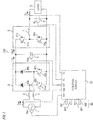
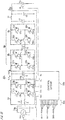
- FIG. 1 is a schematic configuration diagram of the power conversion device according to Embodiment 1 of the present invention.
- the power conversion device 100 includes: a main circuit for converting AC power from a single-phase AC power supply 1 (hereinafter, simply referred to as an AC power supply 1), to DC power, and outputting the DC power to a load 9; and a control circuit 10.
- a main circuit for converting AC power from a single-phase AC power supply 1 hereinafter, simply referred to as an AC power supply 1
- AC power supply 1 a single-phase AC power supply 1
- the main circuit includes: an AC/DC converter 4 for performing power factor correction control for the AC power supply 1 and converting AC power to DC power; a DC/DC converter 6 which is connected to the DC side of the AC/DC converter 4 and performs voltage conversion of the DC power; and a DC capacitor 5 connected between DC buses between the AC/DC converter 4 and the DC/DC converter 6.
- reactors 2 and 3 for current limitation are provided on the input side, and a smoothing capacitor 8 is provided on the output side.
- the AC/DC converter 4 is configured as a semi-bridgeless circuit, and includes semiconductor switching elements 41a, 42a and diode elements 43b, 44b.
- the semiconductor switching elements 41a, 42a are formed from IGBTs (Insulated Gate Bipolar Transistors), to which diodes 41b, 42b are respectively connected in antiparallel.
- the DC/DC converter 6 is configured as a step-down chopper circuit of a non-isolation type, and includes semiconductor switching elements 61 a, 62a, and a reactor 7 for current control.
- the semiconductor switching elements 61a, 62a are formed from IGBTs, to which diodes 61b, 62b are respectively connected in antiparallel.
- the semiconductor switching elements 41 a, 42a, 61a, 62a may be MOSFETs (Metal Oxide Semiconductor Field Effect Transistors) including diodes between the sources and drains, or may be semiconductor switching elements such as thyristors.
- MOSFETs Metal Oxide Semiconductor Field Effect Transistors
- the included diodes may be used as the diodes 41b, 42b, 61b, 62b.
- a P-side terminal of the DC capacitor 5 is connected to a P terminal of the DC output side of the AC/DC converter 4, and a P terminal on the DC input side of the DC/DC converter 6.
- An N-side terminal of the DC capacitor 5 is connected to an N terminal on the DC output side of the AC/DC converter 4, and an N terminal on the DC input side of the DC/DC converter 6.
- the DC capacitor 5 has an energy buffer function, and smooths the difference between power input from the AC/DC converter 4 and power output from the DC/DC converter 6.
- the DC capacitor 5 may be formed from an aluminum electrolytic capacitor, a film capacitor, a ceramic capacitor, a tantalum capacitor, an EDLC (electric double layered capacitor), or the like.
- the DC capacitor 5 may be formed by a battery such as a lithium ion battery.
- the load 9 may be an electric apparatus driven with DC voltage, or a power storage element such as a battery or a capacitor.
- AC voltage vac of the AC power supply 1, voltage vc1 of the DC capacitor 5, and load voltage VL which is voltage of the smoothing capacitor 8, are detected by voltage sensors (not shown), and the detected voltages are input to the control circuit 10. Further, AC current iac of the AC power supply 1 and load current IL are detected by current sensors, and the detected currents are input to the control circuit 10.
- the control circuit 10 generates gate signals 11 (gate signals G41, G42, G61, G62 for the semiconductor switching elements 41a, 42a, 61a, 62a) on the basis of the input voltage current information, to perform output control for the AC/DC converter 4 and the DC/DC converter 6.
- Vac indicates a voltage effective value of the AC power supply 1
- Iac indicates a current effective value of the AC power supply 1
- Vdc indicates a DC voltage component of the DC capacitor 5
- iin indicates input current of the DC capacitor 5
- iout indicates output current of the DC capacitor 5.
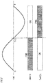
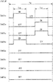
- FIG. 2 is a diagram illustrating operation of the AC/DC converter 4.
- Sw41a and Sw42a indicate the switching states of the semiconductor switching elements 41a and 42a.
- One cycle of the AC power supply 1 is denoted by T.
- voltage vac of the AC power supply 1 has a positive polarity, and the control circuit 10 turns on the semiconductor switching element 42a and performs PWM control for the semiconductor switching element 41a, to perform control so that the input power factor from the AC power supply 1 becomes substantially 1, that is, to control current iac at a high power factor.
- voltage vac of the AC power supply 1 has a negative polarity, and the control circuit 10 turns on the semiconductor switching element 41 a and performs PWM control for the semiconductor switching element 42a, to perform control so that the input power factor from the AC power supply 1 becomes substantially 1, that is, to control current iac at a high power factor.
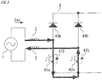
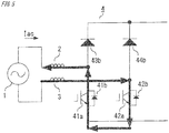
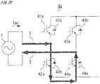
- FIG. 3 to FIG. 6 are current route diagrams illustrating operation of the AC/DC converter 4.
- the semiconductor switching element 42a is kept in an ON state, and when the semiconductor switching element 41a is turned on, the input current is short-circuited via the reactors 2 and 3, and the reactor 2 and the reactor 3 are excited, so that the current increases in the positive direction ( FIG. 3 ). Then, when the semiconductor switching element 41 a is turned off, excitation energy accumulated in the reactor 2 and the reactor 3 is output to the DC capacitor 5 side via the diode 43b. At this time, the current in the reactors 2 and 3 decreases ( FIG. 4 ).
- the semiconductor switching element 41a is kept in an ON state, and when the semiconductor switching element 42a is turned on, the input current is short-circuited via the reactors 2 and 3, and the reactor 2 and the reactor 3 are excited, so that the current increases in the negative direction ( FIG. 5 ). Then, when the semiconductor switching element 42a is turned off, excitation energy accumulated in the reactor 2 and the reactor 3 is output to the DC capacitor 5 side via the diode 44b. At this time, the current in the reactors 2 and 3 decreases ( FIG. 6 ).
- the control circuit 10 performs high power factor control for the input AC current iac by performing ON/OFF control for the semiconductor switching elements 41 a, 42a as described above. It is noted that ideally, the semiconductor switching element 41a and the semiconductor switching element 42a are driven with the same duty cycle.
- a theoretical duty cycle D41 for the semiconductor switching element 41a when the current iac is controlled at a high power factor is shown in the following Expression (1).
- a duty cycle D43 for the diode 43b is represented by Expression (2) on the basis of Expression (1).
- voltage vac of the AC power supply 1 is defined by Expression (3). Therefore, current iin flowing into the DC capacitor 5 can be calculated by Expression (4).
- a step-down chopper circuit is used for the DC/DC converter 6.
- the control circuit 10 performs ON/OFF control for the semiconductor switching elements 61 a, 62a, thereby causing the DC capacitor 5 to output DC power and controlling current IL and voltage VL to the load 9, to be desired values.
- FIG. 7 and FIG. 8 are current route diagrams illustrating operation of the DC/DC converter 6.
- the semiconductor switching element 61 a is turned on, the semiconductor switching element 62a is turned off, and current flows from the DC capacitor 5 to the semiconductor switching element 61 a, the reactor 7, and the load 9 ( FIG. 7 ).
- the semiconductor switching element 61a is turned off.
- the semiconductor switching element 62a is turned on and the semiconductor switching element 61a is turned off from the state in FIG. 7 , current circulates through the semiconductor switching element 62a and the reactor 7 to the load 9, due to the current continuity of the reactor 7 ( FIG. 8 ).
- the control circuit 10 adjusts the duty cycle of the semiconductor switching element 61a and the semiconductor switching element 62a, thereby adjusting power supplied to the load 9, in this case, adjusting the load current IL.
- the DC/DC converter 6 supplies the current IL to the load 9 at the DC voltage VL, thereby supplying DC power to the load 9.
- the current iout output from the DC capacitor 5 is discontinuous with respect to the switching cycles of the semiconductor switching elements 61a, 62a, but can be considered to be current that is continuous, on average, with respect to the cycle T of the AC power supply 1.
- Output current iout of the DC capacitor 5 is assumed to be DC current Idc.
- the voltage relational expression of the DC capacitor 5 can be represented by the following Expression (5).
- Cdc is the electrostatic capacitance of the DC capacitor 5
- vc2 is an AC voltage component (ripple voltage) of the DC capacitor 5.
- the input AC current iac is represented by Expression (6).
- Expression (7) is derived.
- Expression (7) indicates that, if output current iout of the DC capacitor 5 is DC current, the ripple voltage vc2 that has a frequency twice as high as the frequency of the AC power supply 1 necessarily occurs on the DC capacitor 5, by the high power factor control performed in the AC/DC converter 4 connected to the AC power supply 1.
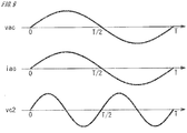
- FIG. 9 shows a waveform diagram of such ripple voltage vc2, and the voltage vac and current iac of the AC power supply 1, as a reference example of the present embodiment. As shown in FIG. 9 , the ripple voltage vc2 greatly varies at a frequency twice as high as the frequency of the AC power supply 1.
- the control circuit 10 intentionally superimposes an AC current component (ripple current) irp onto output current iout of the DC capacitor 5.
- the DC/DC converter 6 is controlled so that an AC current component (ripple current) is generated in current IL output to the load 9, thereby generating ripple current irp in output current iout of the DC capacitor 5.
- FIG. 10 is a waveform diagram showing voltage vac and current iac of the AC power supply 1 and components contained in output current iout of the DC capacitor 5.
- the output current iout of the DC capacitor 5 is current obtained by superimposing ripple current irp onto the DC current component Idc, and the ripple current irp to be superimposed is sinewave current having a frequency twice as high as the frequency of voltage vac of the AC power supply 1.
- the initial phase of the ripple current irp is set such that the ripple current irp has the minimum value at the zero cross phase of the AC power supply 1 and has the maximum value at the peak phase thereof.
- ripple current irp of the DC capacitor 5 is represented by the following Expression (8)
- output current iout is represented by the following Expression (9).
- Irp is the effective value of ripple current irp.
- FIG. 11 is a waveform diagram showing input and output currents of the DC capacitor 5 in the case where the DC capacitor 5 outputs only DC current, as a comparative example. In this case, output current iouta of the DC capacitor 5 becomes the DC current Idc.
- output current iout of the DC capacitor 5 includes the ripple current irp superimposed thereon as described above.
- FIG. 12 is a waveform diagram showing input and output currents of the DC capacitor 5.
- output current iout becomes the minimum value along with input current iin of the DC capacitor 5 becoming almost zero.
- output current iout becomes the maximum value along with input current iin becoming the maximum value.
- the charge/discharge current (iin - iout) which is ripple current, compensated by the DC capacitor 5 can be suppressed, and the ripple voltage vc2 and the ripple current effective value of the DC capacitor 5 can be suppressed.
- An amplitude ⁇ Vdc of ripple voltage vc2 which is an AC voltage component of the DC capacitor 5 is defined by the following Expression (12) on the basis of the above Expression (11).
- ⁇ Vdc Vac ⁇ Iac ⁇ Vdc ⁇ ⁇ 2 Irp / 2 ⁇ Cdc ⁇ Vdc
- Input current iin flowing into the DC capacitor 5 can be represented by the following Expression (13). Since output current iout flowing out from the DC capacitor 5 is represented by the above Expression (9), charge/discharge current (iin - iout) of the DC capacitor 5 is represented by the following Expression (14).
- Expression (13) and Expression (14) can be represented by Expression (13a) and Expression (14a) using load voltage VL and load current IL.
- IL* is a command value for load current IL
- ILrp is the effective value of the ripple current to be generated in the load current IL.
- charge/discharge current (iin - iout) of the DC capacitor 5 becomes a component having a frequency twice as high as the frequency of voltage vac of the AC power supply 1.
- the charge/discharge current (iin - iout) decreases when the peak value ( ⁇ 2)Irp of ripple current irp superimposed on output current iout increases, or the ripple current peak value ( ⁇ 2)ILrp generated in load current IL increases.
- a current component having a carrier frequency of the AC/DC converter 4 and the DC/DC converter 6 flows into or from the DC capacitor 5.
- the charge/discharge current of the DC capacitor 5 is actually defined by the total sum including other frequency components such as the carrier frequency component, as well as the one shown by the above Expression (14a).
- the carrier frequency is dominant and is greatly higher than the power supply frequency of the AC power supply 1, and the current component having the carrier frequency, which flows into or from the DC capacitor 5, is constant without depending on the frequency component twice as high as the frequency of the AC power supply 1.
- the current component shown by Expression (14a) varies but the current component having the carrier frequency is constant. Therefore, in the present embodiment, the current component shown by Expression (14a) is suppressed, and the ripple current converges to the current component having the carrier frequency.
- ripple current irp As described above, by the DC capacitor 5 outputting ripple current irp shown by the above Expression (8), ripple voltage vc2 occurring on the DC capacitor 5 can be suppressed on the basis of the above Expression (11), and charge/discharge current (iin - iout) compensated by the DC capacitor 5 can be suppressed on the basis of the above Expression (14a).
- the ripple current irp output from the DC capacitor 5 is sinewave current having a frequency twice as high as the frequency of voltage vac of the AC power supply 1, and the initial phase of the ripple current irp is set such that the ripple current irp has the minimum value at the zero cross phase and has the maximum value at the peak phase.
- the DC/DC converter 6 causes the DC capacitor 5 to output such ripple current irp.
- control for the AC/DC converter 4 and the DC/DC converter 6 by the control circuit 10 will be described.
- FIG. 13 is a control block diagram showing generation of a gate signal for the AC/DC converter 4, in the control circuit 10.
- the control circuit 10 controls current iac input from the AC power supply 1, at a power factor of 1 with respect to voltage vac of the AC power supply 1. Further, the control circuit 10 selectively performs voltage control for the DC capacitor 5.
- a deviation 21 between a DC voltage command value Vdc* and detected voltage vc1 is subjected to PI control, to generate a current command amplitude 22.
- the current command amplitude 22 is multiplied by a sinewave signal sin ⁇ t having the same phase as voltage vac of the AC power supply 1, to calculate a current command 23.
- a switchover device 25 selects one of the current command 23 and the current command iac* as a current command 26, in accordance with whether or not to perform constant voltage control for the DC capacitor 5.
- a deviation 27 between the current command 26 and detected current iac is subjected to PI control, to calculate a voltage command value 28, and the voltage command value 28 is divided by the DC voltage component Vdc of the DC capacitor 5, thereby calculating a duty cycle 29.
- a PWM circuit 30 generates a gate signal 31 for performing PWM control for the AC/DC converter 4, on the basis of the duty cycle 29.
- the carrier frequency can be arbitrarily adjusted, and a triangle wave, a saw-tooth wave, or the like is used as the carrier wave.
- FIG. 14 is a control block diagram showing generation of gate signals G41, G42 for the respective semiconductor switching elements 41 a, 42a in the AC/DC converter 4, in the control circuit 10.
- the gate signal 31 is input to a selector 32 for the semiconductor switching element 41a, and a selector 38 for the semiconductor switching element 42a.
- a polarity determination device 33 determines the polarity of voltage vac of the AC power supply 1, and outputs a signal 34 which indicates 1 when the voltage vac is positive, and indicates 0 when the voltage vac is negative.
- the selector 32 selects the gate signal 31 when the voltage vac is positive, and selects 1, i.e., an ON signal, when the voltage vac is negative, thus obtaining the gate signal G41.
- the selector 38 selects the gate signal 31, or 1. That is, the selector 38 selects the gate signal 31 when the voltage vac is negative, and selects 1, i.e., an ON signal, when the voltage vac is positive, thus obtaining the gate signal G42.
- the control circuit 10 generates the duty cycle 29 to perform high power factor control for current iac, and as necessary, perform constant voltage control for the DC capacitor 5, and thereby generates the gate signal 31 for the AC/DC converter 4. Then, in accordance with the control shown in FIG. 14 , the control circuit 10 selects one of the semiconductor switching elements 41 a, 42a in response to the polarity of voltage vac of the AC power supply 1, to apply the gate signal 31 to the selected element and control the same, and turns on the other element.
- FIG. 15 is a control block diagram showing generation of gate signals G61, G62 for the respective semiconductor switching elements 61a, 62a in the DC/DC converter 6, in the control circuit 10.
- a command value IL* for load current IL output to the load 9 is a DC current command having only a DC component
- FIG. 15 shows constant current control for supplying constant DC current IL to the load 9.
- an amplitude calculator 50 calculates a ripple current peak value 50a on the basis of the command value IL*.
- the above Expression (11) is a reduction theoretical expression for ripple voltage vc2 of the DC capacitor 5, and the ripple current peak value 50a is calculated using the Expression (11).
- the ripple current peak value ( ⁇ 2)Irp can be calculated on the basis of the amplitude ⁇ Vdc of ripple voltage vc2 of the DC capacitor 5.
- a command value (( ⁇ 2)Irp)* for this ( ⁇ 2)Irp can be calculated from the following Expression (16) using an amplitude target value ⁇ Vdc* for ripple voltage vc2, and the (( ⁇ 2)Irp)* is used as the ripple current peak value 50a.
- the ripple current peak value 50a is a target peak value for ripple current irp to be superimposed onto output current iout of the DC capacitor 5.
- the ripple current peak value 50a may be calculated using the above Expression (14a) which is a reduction theoretical expression for charge/discharge current of the DC capacitor 5.
- Expression (15) which is based on Expression (14a)
- the peak value ( ⁇ 2)ILrp of the ripple current to be generated in the load current IL can be calculated on the basis of the amplitude ⁇ Irp of charge/discharge current of the DC capacitor 5.
- a command value (( ⁇ 2)ILrp)* for this ( ⁇ 2)ILrp can be calculated from the following Expression (17) using an amplitude target value ⁇ Irp* for charge/discharge current of the DC capacitor 5, and the (( ⁇ 2)ILrp)* is used as the ripple current peak value 50a.
- the ripple current peak value 50a is a target peak value for the ripple current to be generated in the load current IL.
- ⁇ 2 ILrp * IL * ⁇ Vdc / VL ⁇ ⁇ Irp *
- a limitation value 51 a is provided for the ripple current peak value 50a.
- a comparator 51 compares the command value IL* for load current IL and a limitation value Lim set in advance for the load 9, and outputs the lower value as the limitation value 51 a.
- the reason for limitation by the command value IL* is to prevent the instantaneous value of current supplied to the load 9 from becoming smaller than 0A, so as not to cause a discontinuous mode.
- the limitation value Lim set for the load 9 is, for example, in the case where the load 9 is assumed to be a battery, a value prescribed from lifetime deterioration due to heat generation of the battery caused by increase in the AC component.
- a comparator 52 compares the ripple current peak value 50a and the limitation value 51 a, and the comparator 52 outputs the lower value as an amplitude 53 of an AC current command.
- the control circuit 10 multiplies the amplitude 53 by a function P shown by the following Expression (18) using ⁇ as the angular frequency of AC voltage vac shown by the above Expression (3), thereby calculating a ripple current command 54 as the AC current command.
- P cos 2 ⁇ t ⁇ ⁇
- the ripple current command 54 generated by multiplying the amplitude 53 by the function P is generated with the phase thereof lagging by ( ⁇ /2) relative to a fundamental sinewave having a frequency 2 ⁇ (2n - 1) times as high as the fundamental frequency of the AC power supply 1.
- P cos 2 2 n ⁇ 1 ⁇ t ⁇ ⁇
- the control circuit 10 adds the calculated ripple current command 54 to the command value IL* for load current IL, thereby generating a current command value 55 containing ripple current, as an output current command for the DC/DC converter 6.
- the current command value 55 is compared with detected load current IL, and the resultant deviation 56 is subjected to PI control, to calculate a voltage command value 57.
- the voltage command value 57 is divided by DC voltage VL of the load 9, to calculate a duty cycle 58.
- a PWM circuit 59 generates a gate signal G61 for the semiconductor switching element 61 a in the DC/DC converter 6.
- An inversion device 60 inverts the gate signal G61, to generate a gate signal G62 for the semiconductor switching element 62a.
- a dead time may be provided for the semiconductor switching elements 41a, 42a in the AC/DC converter 6.
- the semiconductor switching element 62a may be controlled to be constantly OFF. In this case, it is not necessary to set a dead time.
- Only the diode 62b may be provided without providing the semiconductor switching element 62a.
- the control circuit 10 performs current control for the DC/DC converter 6, using the current command value 55 obtained by superimposing, onto the DC current command (command value IL*) for DC current to be supplied to the load 9, the ripple current command 54 which has a frequency 2 ⁇ (2n - 1) times as high as the frequency of the AC power supply 1 and has the minimum value at the zero cross phase and the maximum value at the peak phase.
- the amplitude 53 of the ripple current command 54 is determined on the basis of the amplitude target value for ripple voltage or ripple current (charge/discharge current) of the DC capacitor 5.
- the AC/DC converter 4 is a semi-bridgeless circuit type, but is not limited thereto.
- a power conversion device 100a shown in FIG. 16 as a general AC/DC converter, for example, an AC/DC converter 4a configured from a one-transistor power factor correction (PFC) circuit is used.
- the AC/DC converter 4a is composed of bridge diodes 41b to 44b, a reactor 12, a semiconductor switching element 45a for current control, and a step-up diode 46b.
- a diode 45b is connected in antiparallel to the semiconductor switching element 45a.
- a control circuit 10a generates gate signals 11a (gate signals G45, G61, G62 for the semiconductor switching elements 45a, 61 a, 62a) on the basis of the input voltage current information, to perform output control for the AC/DC converter 4a and the DC/DC converter 6.
- the other configuration is the same as that of the power conversion device 100 according to the above Embodiment 1. Also in this case, the same effect can be provided through the same control as in the power conversion device 100 according to the above Embodiment 1.
- FIG. 17 is a configuration diagram showing a power conversion device 100b using an interleave-type AC/DC converter 4b in which one-transistor power factor correction (PFC) circuits are connected in parallel and the phases are shifted from each other by 180°.
- the AC/DC converter 4b is composed of bridge diodes 41b to 44b and two one-transistor PFC circuits.
- the first one-transistor PFC circuit is composed of a reactor 13, the semiconductor switching element 45a for current control, and a step-up diode 47b.
- the second one-transistor PFC circuit is composed of a reactor 14, a semiconductor switching element 46a for current control, and a step-up diode 48b. Diodes 45b, 46b are respectively connected in antiparallel to the semiconductor switching elements 45a, 46a.
- a control circuit 10b generates gate signals 11b (gate signals G45, G46, G61, G62 for semiconductor switching elements 45a, 46a, 61a, 62a) on the basis of the input voltage current information, to perform output control for the AC/DC converter 4b and the DC/DC converter 6.
- the other configuration is the same as that of the power conversion device 100 according to the above Embodiment 1. Also in this case, the same effect can be provided through the same control as in the power conversion device 100 according to the above Embodiment 1.
- the amplitude 53 of the ripple current command 54 is determined on the basis of the amplitude target value for ripple voltage or ripple current (charge/discharge current) of the DC capacitor 5.
- the amplitude 53 may be determined on the basis of an electrostatic capacitance target value for the DC capacitor 5.
- the ripple current peak value ( ⁇ 2)Irp can be calculated on the basis of the electrostatic capacitance Cdc of the DC capacitor 5. That is, the command value (( ⁇ 2)Irp)* for the ripple current peak value can be calculated using the electrostatic capacitance target value, and the calculated value is used as the ripple current peak value 50a in the control block diagram shown in FIG. 15 . Also in this case, ripple voltage and ripple current of the DC capacitor 5 can be reduced, and thus the same effect can be obtained.
- FIG. 18 is a schematic configuration diagram of the power conversion device according to Embodiment 2 of the present invention.
- the power conversion device 101 includes: a main circuit for converting AC power from the AC power supply 1, to DC power, and outputting the DC power to a load 9a which is a battery load; and a control circuit 10c.
- the main circuit includes: an AC/DC converter 4c for performing power factor correction control for the AC power supply 1 and converting AC power to DC power; a DC/DC converter 6a which is connected to the DC side of the AC/DC converter 4c and performs voltage conversion of the DC power; and the DC capacitor 5 connected between DC buses between the AC/DC converter 4c and the DC/DC converter 6a.
- the DC/DC converter 6a is configured as an isolation-type DC/DC converter, and the load 9a is formed from a battery.
- load voltage VL which is the battery voltage
- voltage Vdc of the DC capacitor 5 which is a link portion between the AC/DC converter 4c and the DC/DC converter 6a can be changed, or power can be regenerated from the load 9a to the AC power supply 1.
- the AC/DC converter 4c has a regeneration function
- the power conversion device 101 is capable of bidirectional power transmission between the AC power supply 1 and the load 9.
- the control circuit 10c has two operation modes which are a power-running mode for performing power-running operation and a regeneration mode for performing regeneration operation, to control the DC/DC converter 6a and the AC/DC converter 4c.
- the AC/DC converter 4c is configured from a full-bridge circuit, and the reactors 2 and 3 for current limitation are provided on the AC side.
- the AC/DC converter 4c includes semiconductor switching elements 41a to 44a, and the semiconductor switching elements 41a to 44a are formed from IGBTs to which the diodes 41b to 44b are connected in antiparallel, respectively.
- the AC/DC converter 4c may be configured as a semi-bridge circuit type, a one-transistor PFC circuit, or an interleave type, as in the above Embodiment 1.
- the DC/DC converter 6a includes a first full-bridge circuit 6b, a second full-bridge circuit 6c, and a transformer 16 connected between the first full-bridge circuit 6b and the second full-bridge circuit 6c.
- the first full-bridge circuit 6b includes semiconductor switching elements 61a to 64a, and the semiconductor switching elements 61a to 64a are formed from IGBTs to which diodes 61b to 64b are connected in antiparallel, respectively.
- the second full-bridge circuit 6c includes semiconductor switching elements 65a to 68a, and the semiconductor switching elements 65a to 68a are formed from IGBTs to which diodes 65b to 68b are connected in antiparallel, respectively.
- the semiconductor switching elements 41 a to 44a, 61 a to 64a, 65a to 68a may be MOSFETs including diodes between the sources and drains, or may be semiconductor switching elements such as thyristors.
- the included diodes may be used as the diodes 41b to 44b, 61b to 64b, 65b to 68b.
- a smoothing capacitor 17, a smoothing reactor 18, and a smoothing capacitor 19 are connected at a stage subsequent to the DC/DC converter 6a, thereby smoothing load current IL flowing to the load 9a.
- a P-side terminal of the DC capacitor 5 is connected to a P terminal of the DC output side of the AC/DC converter 4c, and a P terminal on the DC input side of the first full-bridge circuit 6b of the DC/DC converter 6a.
- An N-side terminal of the DC capacitor 5 is connected to an N terminal on the DC output side of the AC/DC converter 4c, and an N terminal on the DC input side of the first full-bridge circuit 6b of the DC/DC converter 6a.
- the DC capacitor 5 has an energy buffer function, and smooths the difference between power input from the AC/DC converter 4c and power output from the first full-bridge circuit 6b.
- the DC capacitor 5 may be formed by an aluminum electrolytic capacitor, a film capacitor, a ceramic capacitor, a tantalum capacitor, an EDLC (electric double layered capacitor), or the like.
- the DC capacitor 5 may be formed by a battery such as a lithium ion battery.
- AC voltage vac of the AC power supply 1, voltage vc1 of the DC capacitor 5, and load voltage VL which is voltage of the smoothing capacitor 8, are detected by voltage sensors (not shown), and the detected voltages are input to the control circuit 10c. Further, AC current iac of the AC power supply 1 and load current IL are detected by current sensors, and the detected currents are input to the control circuit 10c.
- the control circuit 10c generates gate signals 11c (gate signals G41 to G44, G61 to G64, G65 to G68 for the semiconductor switching elements 41a to 44a, 61a to 64a, 65a to 68a) on the basis of the input voltage current information, to perform output control for the AC/DC converter 4c and the DC/DC converter 6a.
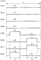
- FIG. 19 is a diagram illustrating operation of the AC/DC converter 4c.
- Sw41 a to Sw44a indicate the switching states of the semiconductor switching elements 41a to 44a, respectively.
- One cycle of the AC power supply 1 is denoted by T.
- voltage vac of the AC power supply 1 has a positive polarity.
- the control circuit 10c turns on the semiconductor switching element 44a and performs PWM control for the semiconductor switching elements 41a, 42a, to control excitation and reset of excitation of the reactors 2 and 3.
- the semiconductor switching element 41a and the semiconductor switching element 42a are in a relationship in which ON and OFF are inverted from each other, that is, when the semiconductor switching element 41 a is turned on, the semiconductor switching element 42a is turned off, and when the semiconductor switching element 42a is turned on, the semiconductor switching element 41 a is turned off.
- the control circuit 10c turns on the semiconductor switching element 42a and performs PWM control for the semiconductor switching elements 43a, 44a, to control excitation and reset of excitation of the reactors 2 and 3.
- the semiconductor switching element 43a and the semiconductor switching element 44a are in a relationship in which ON and OFF are inverted from each other, that is, when the semiconductor switching element 43a is turned on, the semiconductor switching element 44a is turned off, and when the semiconductor switching element 44a is turned on, the semiconductor switching element 43a is turned off.
- dead times may be provided at a gate timing between the semiconductor switching element 41 a and the semiconductor switching element 42a, and at a gate timing between the semiconductor switching element 43a and the semiconductor switching element 44a.
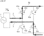
- FIG. 20 to FIG. 23 are current route diagrams illustrating operation of the AC/DC converter 4c.
- the semiconductor switching element 44a is kept in an ON state, and when the semiconductor switching element 42a is turned on, the input current is short-circuited via the reactors 2 and 3, and the reactor 2 and the reactor 3 are excited, so that the current increases in the positive direction ( FIG. 20 ). Then, when the semiconductor switching element 42a is turned off and the semiconductor switching element 41 a is turned on, excitation of the reactor 2 and the reactor 3 is reset and the accumulated excitation energy is output to the DC capacitor 5 side. At this time, the current in the reactors 2 and 3 decreases ( FIG. 21 ).
- the semiconductor switching element 42a is kept in an ON state, and when the semiconductor switching element 44a is turned on, the input current is short-circuited via the reactors 2 and 3, and the reactor 2 and the reactor 3 are excited, so that the current increases in the negative direction ( FIG. 22 ). Then, when the semiconductor switching element 44a is turned off and the semiconductor switching element 43a is turned on, excitation of the reactor 2 and the reactor 3 is reset and the accumulated excitation energy is output to the DC capacitor 5 side. At this time, the current in the reactors 2 and 3 decreases ( FIG. 23 ).
- the control circuit 10c performs ON/OFF control for the semiconductor switching elements 41 a to 44a as described above, to perform high power factor control for AC current iac.
- AC current iac is controlled by adjusting the period of each operation mode shown in FIG. 20 to FIG. 23 so that the power factor becomes 1 with respect to voltage vac of the AC power supply 1.
- AC current iac is controlled by adjusting the period of each operation mode shown in FIG. 20 to FIG. 23 so that the power factor becomes -1 with respect to voltage Vac of the AC power supply 1.
- FIG. 24 is a waveform diagram illustrating power-running operation of the DC/DC converter 6a.
- the control circuit 10c performs PWM control for the first full-bridge circuit 6b, to adjust a power transmission period Ton of power transmission to the transformer 16 and adjust the transmitted power.
- Ton The period during which the semiconductor switching elements 61 a, 64a are turned on at the same time, or the period during which the semiconductor switching elements 62a, 63a are turned on at the same time, is the power transmission period Ton.
- all the switching elements of the second full-bridge circuit 6c are turned off to perform rectification in a diode rectification mode.
- the control circuit 10c may perform ON/OFF control for the semiconductor switching elements 65a to 68a to perform rectification in a synchronous rectification mode.
- the ON/OFF control is performed such that the semiconductor switching element 65a is synchronized with the semiconductor switching element 61 a, the semiconductor switching element 66a is synchronized with the semiconductor switching element 62a, the semiconductor switching element 67a is synchronized with the semiconductor switching element 63a, and the semiconductor switching element 68a is synchronized with the semiconductor switching element 64a.
- FIG. 26 is a waveform diagram illustrating regeneration operation of the DC/DC converter 6a.
- the control circuit 10c performs PWM control for the second full-bridge circuit 6c, to adjust a power transmission period Ton of power transmission to the transformer 16 and adjust the transmitted power.
- Ton The period during which the semiconductor switching elements 65a, 68a are turned on at the same time, or the period during which the semiconductor switching elements 66a, 67a are turned on at the same time, is the power transmission period Ton.
- all the switching elements of the first full-bridge circuit 6b are turned off to perform rectification in a diode rectification mode.
- the control circuit 10c may perform ON/OFF control for the semiconductor switching elements 61 a to 64a to perform rectification in a synchronous rectification mode.
- the ON/OFF control is performed such that the semiconductor switching element 61 a is synchronized with the semiconductor switching element 65a, the semiconductor switching element 62a is synchronized with the semiconductor switching element 66a, the semiconductor switching element 63 a is synchronized with the semiconductor switching element 67a, and the semiconductor switching element 64a is synchronized with the semiconductor switching element 68a.
- Vdcmin VLmax ⁇ TA / 2 / Tonmax ⁇ N 1 / N 2
- An upper limit value for DC voltage Vdc of the DC capacitor 5 is determined from the withstand voltage of circuits parts composing the power conversion device 101, and DC voltage Vdc of the DC capacitor 5 is set between the upper limit value, and the lower limit value Vdcmin determined by the above Expression (22).
- the control circuit 10c adds the ripple current command as the AC current command, to the DC current command which is the command value IL* for load current IL, thereby generating a current command value containing ripple current and controlling the DC/DC converter 6a.
- the ripple current command is a sinewave having a frequency 2 ⁇ (2n - 1) times as high as the frequency of the AC power supply 1 and having such an initial phase that the sinewave has the minimum value at the zero cross phase and the maximum value at the peak phase.
- the amplitude of the ripple current command is determined so as not to exceed the command value IL* for load current IL, on the basis of the amplitude target value for ripple voltage or ripple current (charge/discharge current) of the DC capacitor 5.
- ripple current irp is generated in output current iout of the DC capacitor 5, thereby reducing charge/discharge power of the DC capacitor 5 and reducing ripple voltage and ripple current, in the DC capacitor 5, which have frequency components twice as high as the frequency of the AC power supply 1 (see FIG. 10 to FIG. 12 ).
- the ripple current command to be added in the regeneration operation is a sinewave having a frequency 2 ⁇ (2n - 1) times as high as the frequency of the AC power supply 1 and having such an initial phase that the sinewave has the maximum value at the zero cross phase and the minimum value at the peak phase.
- the amplitude of the ripple current command is the same as in the case of power-running operation.
- the ripple current command generated by multiplying the amplitude by the function P is a command obtained by inverting the polarity of the ripple current command in power-running operation while keeping the amplitude and the initial phase thereof.
- the DC current command (command value IL*) in regeneration operation is a command obtained by inverting the polarity of the DC current command in power-running operation.
- the DC/DC converter 6a is controlled so that an AC current component (ripple current) is generated in current IL output to the load 9a, thereby generating ripple current irp in output current iout of the DC capacitor 5.
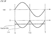
- FIG. 28 is a waveform diagram showing voltage vac and current iac of the AC power supply 1 and components contained in output current iout of the DC capacitor 5, in regeneration operation.
- the output current iout of the DC capacitor 5 is current obtained by superimposing ripple current irp onto the DC current component Idc, and the ripple current irp to be superimposed is sinewave current having a frequency twice as high as the frequency of voltage vac of the AC power supply 1.
- the initial phase of the ripple current irp is set such that the ripple current irp has the maximum value at the zero cross phase of the AC power supply 1 and has the minimum value at the peak phase thereof.
- FIG. 29 is a waveform diagram showing input and output currents of the DC capacitor 5 in regeneration operation in the case where the DC capacitor 5 outputs only DC current, as a comparative example. In this case, output current iouta of the DC capacitor 5 becomes the DC current Idc.
- output current iout of the DC capacitor 5 includes the ripple current irp superimposed thereon as described above.
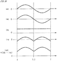
- FIG. 30 shows a waveform diagram of input and output currents of the DC capacitor 5 in regeneration operation.
- the absolute value of output current iout becomes minimum along with input current iin of the DC capacitor 5 becoming almost zero.
- the absolute value of output current iout becomes maximum along with the absolute value of input current iin becoming maximum.
- the charge/discharge current (iin - iout) which is ripple current, compensated by the DC capacitor 5 can be suppressed, and the ripple voltage vc2 and the ripple current effective value of the DC capacitor 5 can be suppressed.
- ripple voltage vc2 in the DC capacitor 5 which has a frequency component twice as high as the frequency of the AC power supply 1 is reduced.
- ripple voltage vc2 is represented by the following Expression (27). It is noted that Expression (27) serves as a reduction theoretical expression for ripple voltage vc2 of the DC capacitor 5 in regeneration operation.
- vc 2 ⁇ Vac ⁇ Iac + Vdc ⁇ ⁇ 2 Irp / 2 ⁇ Cdc ⁇ Vdc ⁇ sin 2 ⁇ t
- charge/discharge current (iin - iout) in the DC capacitor 5 which is ripple current having a frequency component twice as high as the frequency of the AC power supply 1 is reduced in accordance with the above Expression (14a).
- charge/discharge current (iin - iout) of the DC capacitor 5 is a component having a frequency twice as high as the frequency of voltage vac of the AC power supply 1.
- the charge/discharge current (iin - iout) decreases when the peak value ( ⁇ 2)Irp of ripple current irp superimposed on output current iout or the ripple current peak value ( ⁇ 2)ILrp generated in load current IL increases.
- a current component having a carrier frequency of the AC/DC converter 4c and the DC/DC converter 6a flows into or from the DC capacitor 5, and the charge/discharge current of the DC capacitor 5 is actually defined by the total sum including other frequency components such as the carrier frequency component.
- the carrier frequency is dominant and is greatly higher than the power supply frequency of the AC power supply 1, and the current component having the carrier frequency, which flows into or from the DC capacitor 5, is constant without depending on the frequency component twice as high as the frequency of the AC power supply 1. Therefore, in the present embodiment, the current component shown by Expression (30) is suppressed, and the ripple current converges to the current component having the carrier frequency.
- control circuit 10c controls the power factor of the input current iac of the AC power supply 1 to be a high power factor of 1 or -1 and controls DC voltage Vdc of the DC capacitor 5 to be constant.
- control for the DC/DC converter 6a the control circuit 10c controls current transmitted to the load 9a or current transmitted from the load 9a, to be constant, and further, suppresses ripple voltage and ripple current of the DC capacitor 5.
- FIG. 31 is a control block diagram showing generation of a gate signal for the AC/DC converter 4c, in the control circuit 10c.
- a limiter 70 limits the DC voltage command value Vdc* for the DC capacitor 5, by a lower limit value min. As the lower limit value min, the load voltage VL is used. A deviation 71 between a voltage command value 70a for the DC capacitor 5 generated by the limiter 70, and detected voltage vc1, is subjected to PI control, to calculate a current command amplitude 72.
- An operation mode type i.e., the power-running mode or the regeneration mode, is input to a selector 73.
- the selector 73 selects sin ⁇ t in the case of power-running mode, and -sincot in the case of regeneration mode, and outputs the selected one as a sinewave signal 73a. Then, the current command amplitude 72 is multiplied by the sinewave signal 73a, to calculate a current command iac*.
- a deviation 27 between the current command iac* and detected current iac is subjected to PI control, to calculate a voltage command value 28, and the voltage command value 28 is divided by the DC voltage component Vdc of the DC capacitor 5, thereby calculating a duty cycle 29.
- the PWM circuit 30 generates a gate signal 31 for performing PWM control for the AC/DC converter 4, on the basis of the duty cycle 29.
- the carrier frequency can be arbitrarily adjusted, and a triangle wave, a saw-tooth wave, or the like is used as the carrier wave.
- FIG. 32 is a control block diagram showing generation of gate signals G41 to G44 for the respective semiconductor switching elements 41a to 44a in the AC/DC converter 4c, in the control circuit 10c.
- the gate signal 31 is respectively input to a selector 32 for the semiconductor switching elements 41a and 42a, and a selector 38 for the semiconductor switching elements 43 a and 44a.
- a polarity determination device 33 determines the polarity of voltage vac of the AC power supply 1, and outputs a signal 34 which indicates 1 when the voltage vac is positive, and indicates 0 when the voltage vac is negative.
- the selector 32 selects the gate signal 31 when the voltage vac is positive, and selects 1, i.e., an ON signal, when the voltage vac is negative, thus obtaining the gate signal G42.
- the gate signal G42 is inverted to obtain the gate signal G41.
- the selector 38 selects the gate signal 31, or 1. That is, the selector 38 selects the gate signal 31 when the voltage vac is positive, and selects 1, i.e., an ON signal, when the voltage vac is negative, thus obtaining the gate signal G44. In addition, the gate signal G44 is inverted to obtain the gate signal G43.
- FIG. 33 is a control block diagram showing generation of gate signals G61 to G68 for the respective semiconductor switching elements 61a to 68a in the DC/DC converter 6a, in the control circuit 10c.
- a command value IL* for load current IL output to the load 9a is a DC current command having only a DC component, and becomes a positive command value in the case of power-running operation and becomes a negative command value in the case of regeneration operation.
- an amplitude calculator 50 calculates a ripple current peak value 50a on the basis of the command value IL*. That is, using a reduction theoretical expression for ripple voltage vc2 of the DC capacitor 5, calculation can be performed from the above Expression (16) on the basis of the amplitude target value ⁇ Vdc* for ripple voltage vc2, and (( ⁇ 2)Irp)* is used as the ripple current peak value 50a.
- the ripple current peak value 50a may be calculated using the above Expressions (14a), (29) which are reduction theoretical expressions for charge/discharge current of the DC capacitor 5.
- the peak value ( ⁇ 2)ILrp of the ripple current to be generated in the load current IL can be calculated on the basis of the amplitude ⁇ Irp of charge/discharge current of the DC capacitor 5.
- a command value (( ⁇ 2)ILrp)* for this ( ⁇ 2)ILrp can be calculated from the above Expression (17) using an amplitude target value ⁇ Irp* for charge/discharge current of the DC capacitor 5, and the (( ⁇ 2)ILrp)* is used as the ripple current peak value 50a.
- a limitation value 51a is provided for the ripple current peak value 50a.
- a comparator 51 compares the command value IL* for load current IL and a limitation value Lim set in advance for the load 9a, and outputs the lower value as the limitation value 51a.
- the reason for limitation by the command value IL* is to prevent the instantaneous value of current supplied to the load 9a from becoming smaller than 0A, so as not to cause a discontinuous mode.
- the limitation value Lim set for the load 9a is a value prescribed from lifetime deterioration due to heat generation of the battery (load 9a) caused by increase in the AC component.
- a comparator 52 compares the ripple current peak value 50a and the limitation value 51 a, and the comparator 52 outputs the lower value as an amplitude 53 of an AC current command.
- a selector 74 receives an operation mode type, i.e., the power-running mode or the regeneration mode. Using ⁇ as the angular frequency of AC voltage vac shown by the above Expression (3), the selector 74 selects a function P shown by the above Expression (18) in the case of power-running mode and selects a function P shown by the following Expression (31) in the case of regeneration mode, and outputs the selected one as a sinewave signal 74a. The amplitude 53 is multiplied by the sinewave signal 74a, to calculate a ripple current command 54 as the AC current command.
- P ⁇ cos 2 ⁇ t ⁇ ⁇
- the function P used as the sinewave signal 74a by which the amplitude 53 of the AC current command is multiplied may be a function representing a sinewave having the minimum value at the zero cross phase of AC voltage vac and having the maximum value at the peak phase thereof.
- the function P in the regeneration mode, may be a function representing a sinewave having the maximum value at the zero cross phase of AC voltage vac and having the minimum value at the peak phase thereof.
- the control circuit 10c adds the calculated ripple current command 54 to the command value IL* for load current IL, thereby generating a current command value 55 containing ripple current, as an output current command for the DC/DC converter 6a.
- the current command value 55 is compared with detected load current IL, and the resultant deviation 56 is subjected to PI control, to calculate a voltage command value 57.
- the voltage command value 57 is divided by DC voltage VL of the load 9a, to calculate a duty cycle 58.
- a PWM circuit 59 generates gate signals G61 to G68 for the semiconductor switching elements 61 a to 68a in the first full-bridge circuit 6b and the second full-bridge circuit 6c of the DC/DC converter 6a.
- the control circuit 10c calculates, from the duty cycle 58, a diagonal-ON duty for the semiconductor switching elements 61a, 64a, or a diagonal-ON duty for the semiconductor switching elements 62a, 63a, to control the first full-bridge circuit 6b.
- the semiconductor switching elements 61 a, 62a constitute the same leg, and G61 and G62 are set to have the same duty cycle with their phases inverted from each other by 180°.
- the semiconductor switching elements 63a, 64a constitute the same leg, and G63 and G64 are set to have the same duty cycle with their phases inverted from each other by 180°.
- the control circuit 10c controls the semiconductor switching elements 65a to 68a of the second full-bridge circuit 6c in a synchronous rectification mode in the same manner as for the semiconductor switching elements 61 a to 64a of the first full-bridge circuit 6b.
- the PWM circuit 59 generates the gate signals G61, G64 for the semiconductor switching elements 61a, 64a, from the duty cycle 58 and the carrier wave.
- the PWM circuit 59 generates the gate signals G62, G63 for the semiconductor switching elements 62a, 63a, from the carrier wave and a duty cycle 58a obtained by subtracting the duty cycle 58 from 1.
- the gate signals G65 to G68 for the semiconductor switching elements 65a to 68a are the same as the gate signal G61 to G64, respectively.
- the control circuit 10c calculates, from the duty cycle 58, a diagonal-ON duty for the semiconductor switching elements 65a, 68a, or a diagonal-ON duty for the semiconductor switching elements 66a, 67a, to control the second full-bridge circuit 6c.
- the semiconductor switching elements 65a, 66a constitute the same leg, and G65 and G66 are set to have the same duty cycle with their phases inverted from each other by 180°.
- the semiconductor switching elements 67a, 68a constitute the same leg, and G67 and G68 are set to have the same duty cycle with their phases inverted from each other by 180°.
- the control circuit 10c controls the semiconductor switching elements 61a to 64a of the first full-bridge circuit 6b in a synchronous rectification mode in the same manner as for the semiconductor switching elements 65a to 68a of the second full-bridge circuit 6c.
- the PWM circuit 59 generates the gate signals G65, G68 for the semiconductor switching elements 65a, 68a, from the duty cycle 58 and the carrier wave.
- the PWM circuit 59 generates the gate signals G66, G67 for the semiconductor switching elements 66a, 67a, from the carrier wave and the duty cycle 58a obtained by subtracting the duty cycle 58 from 1.
- the gate signal G61 to G64 for the semiconductor switching elements 61 a to 64a are the same as the gate signals G65 to G68, respectively.
- dead times may be provided for the semiconductor switching elements 41a, 42a and the semiconductor switching elements 43a, 44a in the AC/DC converter 4c, respectively. Further, dead times may be provided for the semiconductor switching elements 61a, 62a, the semiconductor switching elements 63 a, 64a, the semiconductor switching elements 65a, 66a, and the semiconductor switching elements 67a, 68a in the DC/DC converter 6a, respectively.
- the isolation-type DC/DC converter 6a using the transformer 16 is used, and the control circuit 10c performs current control for the DC/DC converter 6a, using the current command value 55 obtained by superimposing, onto the DC current command (command value IL*) for DC current to be supplied to the load 9a, the ripple current command 54 having a frequency 2 ⁇ (2n - 1) times as high as the frequency of the AC power supply 1 and having the minimum value at the zero cross phase and the maximum value at the peak phase.
- ripple voltage and ripple current of the DC capacitor 5 can be reduced, and the same effect can be obtained.
- the power conversion device 101 is configured to be capable of bidirectional power transmission, and in regeneration operation, the amplitude, the frequency, and the initial phase of the ripple current command 54 are kept as they are in power-running operation, and the polarities of the ripple current command 54 and the DC current command (command value IL*) are inverted from those in power-running operation.
- the ripple current command 54 is set to be a sinewave having a frequency 2 ⁇ (2n - 1) times as high as the frequency of the AC power supply 1 and having the maximum value at the zero cross phase and the minimum value at the peak phase.
- Switching between power-running operation and regeneration operation is performed by, in the AC/DC converter 4c, only inverting the polarity of the sinewave signal to be multiplied for generating the current command (iac*).
- the switching is performed by only inverting the polarity of the sinewave signal to be multiplied for generating the ripple current command 54.
- the command value for DC voltage Vdc which is necessary for reducing ripple voltage of the DC capacitor 5 in accordance with the above Expression (11), can be set in accordance with the voltage setting range for the DC capacitor 5.
- the reliability of the control is improved, and ripple voltage and ripple current of the DC capacitor 5 can be effectively reduced.
- the ripple current command 54 to be superimposed is a sinewave command.
- a full-wave rectified waveform obtained by folding up a sinewave is used as the ripple current command.
- the circuit configuration of the power conversion device can be achieved by either the above Embodiment 1 or Embodiment 2.
- the case of adopting the above Embodiment 2 which includes bidirectional operations, i.e., power-running operation and regeneration operation, will be described.
- the high power factor control by the AC/DC converter 4c is the same as in the above Embodiment 2.
- FIG. 34 is a waveform diagram showing voltage vac and current iac of the AC power supply 1 and each component contained in output current iout of the DC capacitor 5, in power-running operation.
- Current iac is controlled at a power factor of 1.
- Output current iout of the DC capacitor 5 is current obtained by superimposing ripple current irp onto the DC current component Idc, and the ripple current irp to be superimposed has a full-wave rectified waveform of a sinewave synchronized with AC voltage vac.
- An offset amount (-Q) based on the following Expression (33) is added to the ripple current irp so that the average value thereof becomes 0A, and as a result, the theoretical expression of the ripple current irp is represented by the following Expression (34).
- This ripple current irp has the minimum value at the zero cross phase of the AC power supply 1 and has the maximum value at the peak phase thereof.
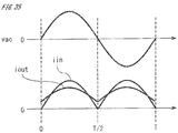
- FIG. 35 is a waveform diagram showing input and output currents of the DC capacitor 5 in power-running operation.
- output current iout becomes the minimum value along with input current iin of the DC capacitor 5 becoming almost zero.
- output current iout becomes the maximum value along with input current iin becoming the maximum value.
- the charge/discharge current (iin - iout) which is ripple current, compensated by the DC capacitor 5 can be suppressed, and the ripple voltage vc2 and the ripple current effective value of the DC capacitor 5 can be suppressed.
- FIG. 36 is a waveform diagram showing voltage vac and current iac of the AC power supply 1 and each component contained in output current iout of the DC capacitor 5, in regeneration operation.
- Current iac is controlled at a power factor of -1.
- Output current iout of the DC capacitor 5 is current obtained by superimposing ripple current irp onto the DC current component Idc, and the ripple current irp to be superimposed has a waveform obtained by inverting the polarity of a full-wave rectified waveform of a sinewave synchronized with AC voltage vac.
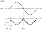
- FIG. 37 is a waveform diagram showing input and output currents of the DC capacitor 5 in regeneration operation.
- the absolute value of output current iout becomes minimum along with input current iin of the DC capacitor 5 becoming almost zero.
- the absolute value of output current iout becomes maximum along with the absolute value of input current iin becoming maximum.
- the charge/discharge current (iin - iout) which is ripple current, compensated by the DC capacitor 5 can be suppressed, and the ripple voltage vc2 and the ripple current effective value of the DC capacitor 5 can be suppressed.
- the frequency component twice as high as the frequency of the AC power supply 1 is focused on, without considering a current component having a carrier frequency of the AC/DC converter 4c and the DC/DC converter 6a.
- FIG. 38 is a control block diagram showing generation of gate signals G61 to G68 for the respective semiconductor switching elements 61a to 68a in the DC/DC converter 6a, in the control circuit 10c according to the present Embodiment 3.
- a command value IL* for load current IL output to the load 9a is a DC current command having only a DC component, and becomes a positive command value in the case of power-running operation and becomes a negative command value in the case of regeneration operation.
- an amplitude calculator 50 calculates the ripple current peak value 50a on the basis of the command value IL*.
- a comparator 52 outputs an amplitude 53 on the basis of the ripple current peak value 50a.
- a selector 75 receives an operation mode type, i.e., the power-running mode or the regeneration mode.
- the selector 75 selects
- a selector 76 receives an operation mode type, i.e., the power-running mode or the regeneration mode, and outputs a coefficient 76a according to the operation mode.
- the amplitude 53 is multiplied by the coefficient 76a, to generate an offset amount 78.
- control circuit 10c adds the offset amount 78 to a current command 77 obtained by multiplying the amplitude 53 by the sinewave rectification signal 75a, to calculate a ripple current command 77a as the AC current command.
- the control circuit 10c adds the calculated ripple current command 77a to the command value IL* for load current IL, thereby generating a current command value 55 containing ripple current, as an output current command for the DC/DC converter 6a.
- the current command value 55 is compared with detected load current IL, and the resultant deviation 56 is subjected to PI control, to calculate a voltage command value 57.
- the voltage command value 57 is divided by DC voltage VL of the load 9a, thereby calculating a duty cycle 58.
- a PWM circuit 59 generates gate signals G61 to G68 for the semiconductor switching elements 61 a to 68a in the first full-bridge circuit 6b and the second full-bridge circuit 6c of the DC/DC converter 6a.
- ripple voltage and ripple current of the DC capacitor 5 can be reduced, and size reduction of the DC capacitor 5 and size reduction and cost reduction of the power conversion device 101 can be achieved.
- a full-wave rectified waveform of a sinewave is used as the ripple current command.
- a triangle wave is used as the ripple current command.
- the circuit configuration of the power conversion device can be achieved by either the above Embodiment 1 or Embodiment 2.
- the case of adopting the above Embodiment 2 which includes bidirectional operations, i.e., power-running operation and regeneration operation, will be described.
- the high power factor control by the AC/DC converter 4c is the same as in the above Embodiment 2.
- FIG. 39 is a waveform diagram showing voltage vac and current iac of the AC power supply 1 and each component contained in output current iout of the DC capacitor 5, in power-running operation.
- Current iac is controlled at a power factor of 1.
- Output current iout of the DC capacitor 5 is current obtained by superimposing ripple current irp onto the DC current component Idc.
- the ripple current irp to be superimposed has a triangle waveform having a frequency twice as high as the frequency of AC voltage vac and having the minimum value at the zero cross phase of AC voltage vac and the maximum value at the peak phase thereof.
- the ripple current irp is set such that the minimum value and the maximum value are equally distant from the zero point so that the average value becomes 0A.
- FIG. 40 is a waveform diagram showing input and output currents of the DC capacitor 5 in power-running operation.
- output current iout becomes the minimum value along with input current iin of the DC capacitor 5 becoming almost zero.
- output current iout becomes the maximum value along with input current iin becoming the maximum value.
- the charge/discharge current (iin - iout) which is ripple current, compensated by the DC capacitor 5 can be suppressed, and the ripple voltage vc2 and the ripple current effective value of the DC capacitor 5 can be suppressed.
- FIG. 41 is a waveform diagram showing voltage vac and current iac of the AC power supply 1 and each component contained in output current iout of the DC capacitor 5, in regeneration operation.
- Current iac is controlled at a power factor of -1.
- Output current iout of the DC capacitor 5 is current obtained by superimposing ripple current irp onto the DC current component Idc.
- the ripple current irp to be superimposed has a triangle waveform having a frequency twice as high as the frequency of AC voltage vac and having the maximum value at the zero cross phase of AC voltage vac and the minimum value at the peak phase thereof.
- the ripple current irp is set such that the minimum value and the maximum value are equally distant from the zero point so that the average value becomes 0A.
- FIG. 42 is a waveform diagram showing input and output currents of the DC capacitor 5 in regeneration operation.
- the absolute value of output current iout becomes minimum along with input current iin of the DC capacitor 5 becoming almost zero.
- the absolute value of output current iout becomes maximum along with the absolute value of input current iin becoming maximum.
- the charge/discharge current (iin - iout) which is ripple current, compensated by the DC capacitor 5 can be suppressed, and the ripple voltage vc2 and the ripple current effective value of the DC capacitor 5 can be suppressed.
- the frequency component twice as high as the frequency of the AC power supply 1 is focused on, without considering a current component having a carrier frequency of the AC/DC converter 4c and the DC/DC converter 6a.
- FIG. 43 is a control block diagram showing generation of gate signals G61 to G68 for the respective semiconductor switching elements 61 a to 68a in the DC/DC converter 6a, in the control circuit 10c according to the present Embodiment 4.
- a command value IL* for load current IL output to the load 9a is a DC current command having only a DC component, and becomes a positive command value in the case of power-running operation and becomes a negative command value in the case of regeneration operation.
- an amplitude calculator 50 calculates the ripple current peak value 50a on the basis of the command value IL*.
- the ripple current peak value 50a corresponds to the peak-to-peak value of the triangle wave.
- a comparator 52 outputs an amplitude 53 corresponding to the peak-to-peak value of the triangle wave, on the basis of the ripple current peak value 50a.
- a selector 80 receives an operation mode type, i.e., the power-running mode or the regeneration mode, and a triangle wave 79 having a frequency twice as high as the frequency of AC voltage vac is selected with a polarity 80a according to the operation mode, thereby outputting a triangle wave signal 79a with the polarity thereof inverted between the power-running mode and the regeneration mode.
- an operation mode type i.e., the power-running mode or the regeneration mode
- the triangle wave signal 79a has the minimum value at the zero cross phase of AC voltage vac and has the maximum value at the peak phase thereof, and this is reversed in the regeneration mode.
- a selector 81 receives an operation mode type, i.e., the power-running mode or the regeneration mode, and outputs a coefficient 81a according to the operation mode.
- the amplitude 53 is multiplied by the coefficient 81 a, to generate an offset amount 82.
- the coefficient 81a is 0.5 in the power-running mode, and -0.5 in the regeneration mode.
- the offset amount 82 is subtracted from a current command 77 obtained by multiplying the amplitude 53 by the triangle wave signal 79a, thereby calculating a ripple current command 77a as the AC current command.
- the control circuit 10c adds the calculated ripple current command 77a to the command value IL* for load current IL, thereby generating a current command value 55 containing ripple current, as an output current command for the DC/DC converter 6a.
- the current command value 55 is compared with detected load current IL, and the resultant deviation 56 is subjected to PI control, to calculate a voltage command value 57.
- the voltage command value 57 is divided by DC voltage VL of the load 9a, thereby calculating a duty cycle 58.
- a PWM circuit 59 generates gate signals G61 to G68 for the semiconductor switching elements 61a to 68a in the first full-bridge circuit 6b and the second full-bridge circuit 6c of the DC/DC converter 6a.
- ripple voltage and ripple current of the DC capacitor 5 can be reduced, and size reduction of the DC capacitor 5 and size reduction and cost reduction of the power conversion device 101 can be achieved.
- the duty cycle for the DC/DC converter 6 is set to be constant, and the voltage command value Vdc* which is a voltage command for the DC capacitor 5 is adjusted to control the AC/DC converter 4.
- FIG. 44 is a waveform diagram showing voltage vac and current iac of the AC power supply 1, the voltage command value Vdc* for the DC capacitor 5, and a duty cycle K for controlling the DC/DC converter 6.
- Voltage vc1 of the DC capacitor 5 is controlled to the voltage command value Vdc* obtained by full-wave-rectifying a sinewave synchronized with AC voltage vac.
- control for the AC/DC converter 4 and the DC/DC converter 6 by the control circuit 10 will be described.
- FIG. 45 is a control block diagram showing generation of a gate signal for the AC/DC converter 4, in the control circuit 10 according to the present Embodiment 5.
- the control circuit 10 controls current iac input from the AC power supply 1, at a power factor of 1 with respect to voltage vac of the AC power supply 1. Further, the control circuit 10 selectively performs voltage control for the DC capacitor 5.
- a peak value 83 for DC voltage Vdc of the DC capacitor 5 is set, and the peak value 83 is multiplied by a sinewave
- the control circuit 10 performs PI control on a deviation 21 between the voltage command value Vdc* and detected voltage vc1, to calculate a current command amplitude 22. Then, the control circuit 10 multiplies the current command amplitude 22 by a sinewave signal sin ⁇ t having the same phase as voltage vac of the AC power supply 1, thereby calculating a current command 23.
- a switchover device 25 selects one of the current command 23 and the current command iac*, as a current command 26, in accordance with whether or not to perform voltage control for the DC capacitor 5.
- the control circuit 10 performs PI control on a deviation 27 between the current command 26 and detected current iac, to calculate a voltage command value 28, and divides the voltage command value 28 by the DC voltage component Vdc of the DC capacitor 5, thereby calculating a duty cycle 29.
- the PWM circuit 30 generates a gate signal 31 for performing PWM control for the AC/DC converter 4, on the basis of the duty cycle 29.
- FIG. 46 is a control block diagram showing generation of gate signals for the DC/DC converter 6.
- a PWM circuit 84 generates a gate signal G61 for the semiconductor switching element 61a in the DC/DC converter 6, on the basis of a fixed duty cycle K and using a carrier signal.
- an inversion device inverts the gate signal G61 to obtain a gate signal G62 for the semiconductor switching element 62a.
- the voltage command value Vdc* for the DC capacitor 5, which is used for output control for the AC/DC converter 4, contains an AC voltage component, and is generated by multiplying the peak value 83 by the sinewave
- ripple voltage having a frequency twice as high as the frequency of AC voltage vac is arbitrarily generated on the DC capacitor 5.
- a voltage difference between AC voltage vac and voltage vc1 of the DC capacitor 5 within the switching cycle is significantly reduced.
- the amount of power compensated by the DC capacitor 5 within the switching cycle is greatly reduced, whereby a necessary capacitance of the capacitor can be reduced.
Landscapes
- Engineering & Computer Science (AREA)
- Power Engineering (AREA)
- Rectifiers (AREA)
- Dc-Dc Converters (AREA)
Applications Claiming Priority (2)
| Application Number | Priority Date | Filing Date | Title |
|---|---|---|---|
| JP2014228831 | 2014-11-11 | ||
| PCT/JP2015/074873 WO2016075996A1 (fr) | 2014-11-11 | 2015-09-01 | Dispositif de conversion de puissance |
Publications (3)
| Publication Number | Publication Date |
|---|---|
| EP3220531A1 true EP3220531A1 (fr) | 2017-09-20 |
| EP3220531A4 EP3220531A4 (fr) | 2018-07-18 |
| EP3220531B1 EP3220531B1 (fr) | 2024-09-25 |
Family
ID=55954090
Family Applications (1)
| Application Number | Title | Priority Date | Filing Date |
|---|---|---|---|
| EP15859954.8A Active EP3220531B1 (fr) | 2014-11-11 | 2015-09-01 | Dispositif de conversion de puissance |
Country Status (5)
| Country | Link |
|---|---|
| US (1) | US9882466B2 (fr) |
| EP (1) | EP3220531B1 (fr) |
| JP (1) | JP6026049B2 (fr) |
| CN (1) | CN107078665B (fr) |
| WO (1) | WO2016075996A1 (fr) |
Cited By (1)
| Publication number | Priority date | Publication date | Assignee | Title |
|---|---|---|---|---|
| WO2020043689A1 (fr) * | 2018-08-30 | 2020-03-05 | Brusa Elektronik Ag | Dispositif adaptateur pour alimentation bidirectionnelle |
Families Citing this family (50)
| Publication number | Priority date | Publication date | Assignee | Title |
|---|---|---|---|---|
| JP3151194B2 (ja) | 1999-03-19 | 2001-04-03 | 株式会社ジャパンエナジー | コバルトの精製方法 |
| WO2017053330A1 (fr) * | 2015-09-22 | 2017-03-30 | Schlumberger Technology Corporation | Système générateur de fond de trou |
| JP6579893B2 (ja) * | 2015-09-30 | 2019-09-25 | キヤノン株式会社 | 振動型アクチュエータの制御装置と制御方法、駆動装置、撮像装置及び自動ステージ |
| US10511218B2 (en) | 2015-12-22 | 2019-12-17 | Mitsubishi Electric Corporation | Gate drive circuit, that supplies power to a gate of a semiconductor switching element, and carries out a driving on and off of the gate |
| US10454364B2 (en) * | 2016-01-29 | 2019-10-22 | Mitsubishi Electric Corporation | Power convertor |
| WO2017138103A1 (fr) * | 2016-02-10 | 2017-08-17 | 田淵電機株式会社 | Dispositif de commande de fonctionnement autonome, conditionneur de puissance et procédé de commande de fonctionnement autonome |
| US10284132B2 (en) | 2016-04-15 | 2019-05-07 | Emerson Climate Technologies, Inc. | Driver for high-frequency switching voltage converters |
| US10656026B2 (en) | 2016-04-15 | 2020-05-19 | Emerson Climate Technologies, Inc. | Temperature sensing circuit for transmitting data across isolation barrier |
| US9933842B2 (en) | 2016-04-15 | 2018-04-03 | Emerson Climate Technologies, Inc. | Microcontroller architecture for power factor correction converter |
| US10763740B2 (en) | 2016-04-15 | 2020-09-01 | Emerson Climate Technologies, Inc. | Switch off time control systems and methods |
| US10305373B2 (en) | 2016-04-15 | 2019-05-28 | Emerson Climate Technologies, Inc. | Input reference signal generation systems and methods |
| US10312798B2 (en) | 2016-04-15 | 2019-06-04 | Emerson Electric Co. | Power factor correction circuits and methods including partial power factor correction operation for boost and buck power converters |
| US10277115B2 (en) | 2016-04-15 | 2019-04-30 | Emerson Climate Technologies, Inc. | Filtering systems and methods for voltage control |
| KR101846682B1 (ko) * | 2016-06-28 | 2018-04-09 | 현대자동차주식회사 | 전기차량의 충전제어방법 및 그 시스템 |
| KR101908405B1 (ko) * | 2017-02-14 | 2018-10-16 | (주)로드피아 | 아노다이징 처리용 전원 제어 장치 및 그 방법 |
| US12176805B2 (en) * | 2017-03-21 | 2024-12-24 | The Regents Of The University Of Colorado, A Body Corporate | Control architecture for ac-dc and dc-ac conversion capable of bidirectional active and reactive power processing |
| JP6884637B2 (ja) * | 2017-05-18 | 2021-06-09 | 株式会社豊田中央研究所 | 電気回路 |
| JP6444453B2 (ja) * | 2017-06-01 | 2018-12-26 | 三菱電機株式会社 | 電力変換装置の制御装置および制御方法 |
| CN109494983A (zh) * | 2017-09-13 | 2019-03-19 | 株洲中车时代电气股份有限公司 | 一种直流变换器 |
| JP6963487B2 (ja) * | 2017-12-14 | 2021-11-10 | シャープ株式会社 | Dc/dcコンバータ |
| JP6497489B1 (ja) * | 2018-02-02 | 2019-04-10 | 三菱電機株式会社 | 電力変換装置 |
| CN108263240B (zh) * | 2018-02-28 | 2023-08-22 | 深圳市鼎硕同邦科技有限公司 | 电动汽车车载充电装置及其充电方法 |
| CN108306528A (zh) * | 2018-03-20 | 2018-07-20 | 广州京善电子有限公司 | 高压充电电源装置 |
| JP6898882B2 (ja) * | 2018-04-09 | 2021-07-07 | 株式会社Soken | 電力変換装置の制御装置 |
| US11075588B2 (en) * | 2018-05-01 | 2021-07-27 | Transportation Ip Holdings, Llc | Inverter systems |
| SG11202011091QA (en) * | 2018-05-10 | 2020-12-30 | Toshiba Kk | Dc transformation system |
| JP6913056B2 (ja) * | 2018-05-29 | 2021-08-04 | 株式会社Soken | 電力変換装置の制御装置 |
| CN110549880A (zh) * | 2018-05-31 | 2019-12-10 | 联合汽车电子有限公司 | 一种电动汽车混合能量模块化充电系统 |
| JP6842092B2 (ja) * | 2018-05-31 | 2021-03-17 | 国立大学法人 東京大学 | 電源回路、および振動発電装置 |
| DE112019003059T5 (de) * | 2018-06-18 | 2021-03-04 | Keihin Corporation | Umrichtervorrichtung |
| WO2020024252A1 (fr) * | 2018-08-03 | 2020-02-06 | 深圳欣锐科技股份有限公司 | Circuit d'alimentation électrique |
| WO2020115800A1 (fr) * | 2018-12-03 | 2020-06-11 | 三菱電機株式会社 | Dispositif de conversion de puissance |
| JP6529707B1 (ja) * | 2018-12-13 | 2019-06-12 | 三菱電機株式会社 | 電力変換装置 |
| US10996728B2 (en) * | 2019-01-04 | 2021-05-04 | Sigmasense, Llc. | Power supply signal conditioning system based on drive-sense circuit (DSC) processing |
| EP3799282A1 (fr) * | 2019-09-27 | 2021-03-31 | Siemens Aktiengesellschaft | Convertisseur de courant à amortissement actif de la tension d'un circuit intermédiaire |
| JP7183445B2 (ja) * | 2019-10-09 | 2022-12-05 | 三菱電機株式会社 | 電力変換装置 |
| US11368037B2 (en) * | 2019-11-13 | 2022-06-21 | Lear Corporation | On-board charger (OBC) single-stage converter |
| CN111342685B (zh) * | 2020-03-17 | 2021-06-15 | 美的集团股份有限公司 | 升降压驱动电路、方法、空调器和计算机可读存储介质 |
| CN111313728B (zh) * | 2020-03-17 | 2025-11-28 | 美的集团股份有限公司 | 升降压驱动电路、方法、空调器和计算机可读存储介质 |
| WO2021184921A1 (fr) * | 2020-03-17 | 2021-09-23 | 美的集团股份有限公司 | Procédé et circuit de commande survolteur-dévolteur, climatiseur et support de stockage lisible par ordinateur |
| CN111245262B (zh) * | 2020-03-17 | 2021-05-11 | 美的集团股份有限公司 | 升降压驱动电路、空调器、方法和计算机可读存储介质 |
| CN111355416B (zh) * | 2020-04-16 | 2025-06-24 | 广东美的制冷设备有限公司 | 电机驱动控制电路、驱动方法、线路板及空调器 |
| JP7130024B2 (ja) | 2020-11-12 | 2022-09-02 | 三菱電機株式会社 | 電力変換装置 |
| TWI750012B (zh) * | 2021-01-20 | 2021-12-11 | 群光電能科技股份有限公司 | 電源供應裝置及電壓轉換方法 |
| CN113394752B (zh) * | 2021-06-16 | 2023-02-17 | Tcl空调器(中山)有限公司 | 电容器母线电压控制方法、装置、设备和计算机存储介质 |
| US11777414B2 (en) * | 2021-07-02 | 2023-10-03 | Schneider Electric It Corporation | Interleaved power conversion systems and methods |
| WO2023037470A1 (fr) * | 2021-09-09 | 2023-03-16 | 三菱電機株式会社 | Système de climatisation |
| JP7463420B2 (ja) * | 2022-03-10 | 2024-04-08 | 矢崎総業株式会社 | 電力変換装置 |
| JP7828823B2 (ja) * | 2022-04-28 | 2026-03-12 | 日産自動車株式会社 | 電力変換回路 |
| CN115276410A (zh) * | 2022-08-19 | 2022-11-01 | 悦利电气(江苏)有限公司 | 升压变换电路及其工作方法 |
Family Cites Families (21)
| Publication number | Priority date | Publication date | Assignee | Title |
|---|---|---|---|---|
| JP2002010626A (ja) * | 2000-06-16 | 2002-01-11 | Mitsubishi Heavy Ind Ltd | 直流安定化電源 |
| JP2002252986A (ja) * | 2001-02-26 | 2002-09-06 | Canon Inc | インバータ、電源システム及び電源システムにおける漏れ電流低減方法 |
| JP2002291260A (ja) | 2001-03-26 | 2002-10-04 | Mitsubishi Electric Corp | モータ制御装置及びこれを用いた圧縮機 |
| TWI291282B (en) * | 2002-06-03 | 2007-12-11 | Fuji Electric Co Ltd | Power converter |
| US7289341B2 (en) * | 2004-12-14 | 2007-10-30 | Advanced Energy Industries, Inc. | Power supply adaptive feedforward control circuit |
| JP4542483B2 (ja) * | 2005-08-31 | 2010-09-15 | 日立コンピュータ機器株式会社 | スイッチング電源装置及びディスクアレイシステム |
| CN201087938Y (zh) * | 2007-09-10 | 2008-07-16 | 天津理工大学 | 基于dsp控制的双向升降压直直变换器装置 |
| CN101227149A (zh) * | 2007-11-26 | 2008-07-23 | 谢步明 | Dc/dc变换器输出电压纹波调节装置 |
| KR20100136305A (ko) * | 2009-06-18 | 2010-12-28 | 페어차일드코리아반도체 주식회사 | 주파수 변조 제어 장치, 이를 포함하는 스위치 모드 파워 서플라이 및 스위칭 동작 주파수 변조 방법 |
| JP4795478B1 (ja) * | 2010-07-01 | 2011-10-19 | ファナック株式会社 | ワイヤカット放電加工機用のトルクモータ駆動装置 |
| JP2013532944A (ja) * | 2010-07-26 | 2013-08-19 | ネイ・リー・ピーティーイー・リミテッド | Ac/dc低電圧電力供給装置及びac/dc電圧を降圧する方法 |
| CN102751861A (zh) * | 2011-04-21 | 2012-10-24 | 艾默生网络能源系统北美公司 | 一种无桥功率因数校正电路 |
| JP5773435B2 (ja) | 2011-10-25 | 2015-09-02 | ニチコン株式会社 | 充電装置 |
| JP5370519B2 (ja) * | 2012-03-15 | 2013-12-18 | 富士電機株式会社 | 電力変換装置 |
| JP5803945B2 (ja) * | 2012-05-10 | 2015-11-04 | 株式会社日本自動車部品総合研究所 | 電力変換装置 |
| JP5538658B2 (ja) * | 2012-05-24 | 2014-07-02 | 三菱電機株式会社 | 電力変換装置 |
| US8861230B2 (en) * | 2012-05-30 | 2014-10-14 | Astec International Limited | Control circuits for power converters |
| WO2014115618A1 (fr) * | 2013-01-22 | 2014-07-31 | 株式会社 村田製作所 | Source d'alimentation électrique à commutation et système de conversion de courant alternatif en courant continu |
| JP5987786B2 (ja) | 2013-06-05 | 2016-09-07 | 株式会社日本自動車部品総合研究所 | 電力変換装置 |
| DE112015002279B4 (de) * | 2014-05-15 | 2025-07-24 | Mitsubishi Electric Corporation | Energie-umsetzungsvorrichtung |
| EP3151361B1 (fr) * | 2014-05-30 | 2020-09-23 | Fuji Electric Co., Ltd. | Chargeur |
-
2015
- 2015-09-01 EP EP15859954.8A patent/EP3220531B1/fr active Active
- 2015-09-01 CN CN201580052616.6A patent/CN107078665B/zh active Active
- 2015-09-01 US US15/504,555 patent/US9882466B2/en active Active
- 2015-09-01 WO PCT/JP2015/074873 patent/WO2016075996A1/fr not_active Ceased
- 2015-09-01 JP JP2016503867A patent/JP6026049B2/ja active Active
Cited By (2)
| Publication number | Priority date | Publication date | Assignee | Title |
|---|---|---|---|---|
| WO2020043689A1 (fr) * | 2018-08-30 | 2020-03-05 | Brusa Elektronik Ag | Dispositif adaptateur pour alimentation bidirectionnelle |
| US11532999B2 (en) | 2018-08-30 | 2022-12-20 | Brusa Hypower Ag | Adapter device for bidirectional operation |
Also Published As
| Publication number | Publication date |
|---|---|
| CN107078665B (zh) | 2019-08-16 |
| JP6026049B2 (ja) | 2016-11-16 |
| CN107078665A (zh) | 2017-08-18 |
| WO2016075996A1 (fr) | 2016-05-19 |
| US20170244317A1 (en) | 2017-08-24 |
| JPWO2016075996A1 (ja) | 2017-04-27 |
| EP3220531A4 (fr) | 2018-07-18 |
| EP3220531B1 (fr) | 2024-09-25 |
| US9882466B2 (en) | 2018-01-30 |
Similar Documents
| Publication | Publication Date | Title |
|---|---|---|
| EP3220531A1 (fr) | Dispositif de conversion de puissance | |
| JP6569839B1 (ja) | 電力変換装置 | |
| US9401655B2 (en) | Power conversion apparatus with inverter circuit and series converter circuit having power factor control | |
| US10742128B2 (en) | Parallel power supply device | |
| JP5279797B2 (ja) | 電力変換装置 | |
| US7613018B2 (en) | Apparatus and method for supplying DC power source | |
| US8649196B2 (en) | Power converting apparatus with an output voltage that is the sum of voltages generated by individual inverters | |
| US8243482B2 (en) | Control device for matrix converter | |
| US7532491B2 (en) | Apparatus and method for supplying DC power source | |
| US11817768B2 (en) | Power conversion device that can suppress interference between control of input current from an AC power supply and voltage control for a DC capacitor | |
| US8154893B2 (en) | Three-phase power converting apparatus | |
| US9419542B2 (en) | Inverter device | |
| JP5254357B2 (ja) | 電力変換装置 | |
| US10164546B2 (en) | Electric power conversion device | |
| EP1921740A2 (fr) | Commande d'un onduleur | |
| US10615680B2 (en) | Control apparatus for power converter | |
| US9800177B2 (en) | Conversion device | |
| JP6131360B1 (ja) | 電力変換装置 | |
| JP5523508B2 (ja) | 電力変換装置 | |
| US10348190B2 (en) | Conversion device for converting voltage in a non-insulated manner and method for controlling the same | |
| US11183944B2 (en) | Control apparatus for power converter | |
| JP6113248B1 (ja) | 電力変換装置 |
Legal Events
| Date | Code | Title | Description |
|---|---|---|---|
| STAA | Information on the status of an ep patent application or granted ep patent |
Free format text: STATUS: THE INTERNATIONAL PUBLICATION HAS BEEN MADE |
|
| PUAI | Public reference made under article 153(3) epc to a published international application that has entered the european phase |
Free format text: ORIGINAL CODE: 0009012 |
|
| STAA | Information on the status of an ep patent application or granted ep patent |
Free format text: STATUS: REQUEST FOR EXAMINATION WAS MADE |
|
| 17P | Request for examination filed |
Effective date: 20170509 |
|
| AK | Designated contracting states |
Kind code of ref document: A1 Designated state(s): AL AT BE BG CH CY CZ DE DK EE ES FI FR GB GR HR HU IE IS IT LI LT LU LV MC MK MT NL NO PL PT RO RS SE SI SK SM TR |
|
| AX | Request for extension of the european patent |
Extension state: BA ME |
|
| DAV | Request for validation of the european patent (deleted) | ||
| DAX | Request for extension of the european patent (deleted) | ||
| A4 | Supplementary search report drawn up and despatched |
Effective date: 20180618 |
|
| RIC1 | Information provided on ipc code assigned before grant |
Ipc: H02M 7/797 20060101ALI20180612BHEP Ipc: H02M 1/42 20070101AFI20180612BHEP Ipc: H02M 7/12 20060101ALI20180612BHEP Ipc: H02M 1/08 20060101ALN20180612BHEP Ipc: H02M 3/155 20060101ALI20180612BHEP Ipc: H02M 3/158 20060101ALN20180612BHEP Ipc: H02M 3/28 20060101ALI20180612BHEP Ipc: H02M 1/14 20060101ALI20180612BHEP Ipc: H02M 7/04 20060101ALI20180612BHEP |
|
| STAA | Information on the status of an ep patent application or granted ep patent |
Free format text: STATUS: EXAMINATION IS IN PROGRESS |
|
| 17Q | First examination report despatched |
Effective date: 20190320 |
|
| GRAP | Despatch of communication of intention to grant a patent |
Free format text: ORIGINAL CODE: EPIDOSNIGR1 |
|
| STAA | Information on the status of an ep patent application or granted ep patent |
Free format text: STATUS: GRANT OF PATENT IS INTENDED |
|
| RIC1 | Information provided on ipc code assigned before grant |
Ipc: H02M 1/00 20060101ALN20231018BHEP Ipc: H02M 3/158 20060101ALN20231018BHEP Ipc: H02M 1/08 20060101ALN20231018BHEP Ipc: H02M 7/04 20060101ALI20231018BHEP Ipc: H02M 7/12 20060101ALI20231018BHEP Ipc: H02M 3/28 20060101ALI20231018BHEP Ipc: H02M 3/155 20060101ALI20231018BHEP Ipc: H02M 7/797 20060101ALI20231018BHEP Ipc: H02M 1/14 20060101ALI20231018BHEP Ipc: H02M 1/42 20070101AFI20231018BHEP |
|
| RIC1 | Information provided on ipc code assigned before grant |
Ipc: H02M 1/00 20060101ALN20231024BHEP Ipc: H02M 3/158 20060101ALN20231024BHEP Ipc: H02M 1/08 20060101ALN20231024BHEP Ipc: H02M 7/04 20060101ALI20231024BHEP Ipc: H02M 7/12 20060101ALI20231024BHEP Ipc: H02M 3/28 20060101ALI20231024BHEP Ipc: H02M 3/155 20060101ALI20231024BHEP Ipc: H02M 7/797 20060101ALI20231024BHEP Ipc: H02M 1/14 20060101ALI20231024BHEP Ipc: H02M 1/42 20070101AFI20231024BHEP |
|
| INTG | Intention to grant announced |
Effective date: 20231113 |
|
| GRAJ | Information related to disapproval of communication of intention to grant by the applicant or resumption of examination proceedings by the epo deleted |
Free format text: ORIGINAL CODE: EPIDOSDIGR1 |
|
| STAA | Information on the status of an ep patent application or granted ep patent |
Free format text: STATUS: EXAMINATION IS IN PROGRESS |
|
| INTC | Intention to grant announced (deleted) | ||
| GRAP | Despatch of communication of intention to grant a patent |
Free format text: ORIGINAL CODE: EPIDOSNIGR1 |
|
| STAA | Information on the status of an ep patent application or granted ep patent |
Free format text: STATUS: GRANT OF PATENT IS INTENDED |
|
| GRAJ | Information related to disapproval of communication of intention to grant by the applicant or resumption of examination proceedings by the epo deleted |
Free format text: ORIGINAL CODE: EPIDOSDIGR1 |
|
| STAA | Information on the status of an ep patent application or granted ep patent |
Free format text: STATUS: EXAMINATION IS IN PROGRESS |
|
| INTG | Intention to grant announced |
Effective date: 20240426 |
|
| RIC1 | Information provided on ipc code assigned before grant |
Ipc: H02M 1/00 20060101ALN20240412BHEP Ipc: H02M 3/158 20060101ALN20240412BHEP Ipc: H02M 1/08 20060101ALN20240412BHEP Ipc: H02M 7/04 20060101ALI20240412BHEP Ipc: H02M 7/12 20060101ALI20240412BHEP Ipc: H02M 3/28 20060101ALI20240412BHEP Ipc: H02M 3/155 20060101ALI20240412BHEP Ipc: H02M 7/797 20060101ALI20240412BHEP Ipc: H02M 1/14 20060101ALI20240412BHEP Ipc: H02M 1/42 20070101AFI20240412BHEP |
|
| INTC | Intention to grant announced (deleted) | ||
| GRAP | Despatch of communication of intention to grant a patent |
Free format text: ORIGINAL CODE: EPIDOSNIGR1 |
|
| STAA | Information on the status of an ep patent application or granted ep patent |
Free format text: STATUS: GRANT OF PATENT IS INTENDED |
|
| RIC1 | Information provided on ipc code assigned before grant |
Ipc: H02M 1/00 20060101ALN20240620BHEP Ipc: H02M 3/158 20060101ALN20240620BHEP Ipc: H02M 1/08 20060101ALN20240620BHEP Ipc: H02M 7/04 20060101ALI20240620BHEP Ipc: H02M 7/12 20060101ALI20240620BHEP Ipc: H02M 3/28 20060101ALI20240620BHEP Ipc: H02M 3/155 20060101ALI20240620BHEP Ipc: H02M 7/797 20060101ALI20240620BHEP Ipc: H02M 1/14 20060101ALI20240620BHEP Ipc: H02M 1/42 20070101AFI20240620BHEP |
|
| INTG | Intention to grant announced |
Effective date: 20240704 |
|
| GRAS | Grant fee paid |
Free format text: ORIGINAL CODE: EPIDOSNIGR3 |
|
| GRAA | (expected) grant |
Free format text: ORIGINAL CODE: 0009210 |
|
| STAA | Information on the status of an ep patent application or granted ep patent |
Free format text: STATUS: THE PATENT HAS BEEN GRANTED |
|
| AK | Designated contracting states |
Kind code of ref document: B1 Designated state(s): AL AT BE BG CH CY CZ DE DK EE ES FI FR GB GR HR HU IE IS IT LI LT LU LV MC MK MT NL NO PL PT RO RS SE SI SK SM TR |
|
| REG | Reference to a national code |
Ref country code: GB Ref legal event code: FG4D |
|
| REG | Reference to a national code |
Ref country code: CH Ref legal event code: EP |
|
| REG | Reference to a national code |
Ref country code: DE Ref legal event code: R096 Ref document number: 602015090000 Country of ref document: DE |
|
| REG | Reference to a national code |
Ref country code: IE Ref legal event code: FG4D |
|
| REG | Reference to a national code |
Ref country code: LT Ref legal event code: MG9D |
|
| PG25 | Lapsed in a contracting state [announced via postgrant information from national office to epo] |
Ref country code: NO Free format text: LAPSE BECAUSE OF FAILURE TO SUBMIT A TRANSLATION OF THE DESCRIPTION OR TO PAY THE FEE WITHIN THE PRESCRIBED TIME-LIMIT Effective date: 20241225 |
|
| PG25 | Lapsed in a contracting state [announced via postgrant information from national office to epo] |
Ref country code: GR Free format text: LAPSE BECAUSE OF FAILURE TO SUBMIT A TRANSLATION OF THE DESCRIPTION OR TO PAY THE FEE WITHIN THE PRESCRIBED TIME-LIMIT Effective date: 20241226 Ref country code: FI Free format text: LAPSE BECAUSE OF FAILURE TO SUBMIT A TRANSLATION OF THE DESCRIPTION OR TO PAY THE FEE WITHIN THE PRESCRIBED TIME-LIMIT Effective date: 20240925 |
|
| PG25 | Lapsed in a contracting state [announced via postgrant information from national office to epo] |
Ref country code: BG Free format text: LAPSE BECAUSE OF FAILURE TO SUBMIT A TRANSLATION OF THE DESCRIPTION OR TO PAY THE FEE WITHIN THE PRESCRIBED TIME-LIMIT Effective date: 20240925 |
|
| PG25 | Lapsed in a contracting state [announced via postgrant information from national office to epo] |
Ref country code: LV Free format text: LAPSE BECAUSE OF FAILURE TO SUBMIT A TRANSLATION OF THE DESCRIPTION OR TO PAY THE FEE WITHIN THE PRESCRIBED TIME-LIMIT Effective date: 20240925 |
|
| PG25 | Lapsed in a contracting state [announced via postgrant information from national office to epo] |
Ref country code: RS Free format text: LAPSE BECAUSE OF FAILURE TO SUBMIT A TRANSLATION OF THE DESCRIPTION OR TO PAY THE FEE WITHIN THE PRESCRIBED TIME-LIMIT Effective date: 20241225 |
|
| REG | Reference to a national code |
Ref country code: NL Ref legal event code: MP Effective date: 20240925 |
|
| PG25 | Lapsed in a contracting state [announced via postgrant information from national office to epo] |
Ref country code: RS Free format text: LAPSE BECAUSE OF FAILURE TO SUBMIT A TRANSLATION OF THE DESCRIPTION OR TO PAY THE FEE WITHIN THE PRESCRIBED TIME-LIMIT Effective date: 20241225 Ref country code: NO Free format text: LAPSE BECAUSE OF FAILURE TO SUBMIT A TRANSLATION OF THE DESCRIPTION OR TO PAY THE FEE WITHIN THE PRESCRIBED TIME-LIMIT Effective date: 20241225 Ref country code: LV Free format text: LAPSE BECAUSE OF FAILURE TO SUBMIT A TRANSLATION OF THE DESCRIPTION OR TO PAY THE FEE WITHIN THE PRESCRIBED TIME-LIMIT Effective date: 20240925 Ref country code: GR Free format text: LAPSE BECAUSE OF FAILURE TO SUBMIT A TRANSLATION OF THE DESCRIPTION OR TO PAY THE FEE WITHIN THE PRESCRIBED TIME-LIMIT Effective date: 20241226 Ref country code: FI Free format text: LAPSE BECAUSE OF FAILURE TO SUBMIT A TRANSLATION OF THE DESCRIPTION OR TO PAY THE FEE WITHIN THE PRESCRIBED TIME-LIMIT Effective date: 20240925 Ref country code: BG Free format text: LAPSE BECAUSE OF FAILURE TO SUBMIT A TRANSLATION OF THE DESCRIPTION OR TO PAY THE FEE WITHIN THE PRESCRIBED TIME-LIMIT Effective date: 20240925 |
|
| REG | Reference to a national code |
Ref country code: AT Ref legal event code: MK05 Ref document number: 1727491 Country of ref document: AT Kind code of ref document: T Effective date: 20240925 |
|
| PG25 | Lapsed in a contracting state [announced via postgrant information from national office to epo] |
Ref country code: NL Free format text: LAPSE BECAUSE OF FAILURE TO SUBMIT A TRANSLATION OF THE DESCRIPTION OR TO PAY THE FEE WITHIN THE PRESCRIBED TIME-LIMIT Effective date: 20240925 |
|
| PG25 | Lapsed in a contracting state [announced via postgrant information from national office to epo] |
Ref country code: IS Free format text: LAPSE BECAUSE OF FAILURE TO SUBMIT A TRANSLATION OF THE DESCRIPTION OR TO PAY THE FEE WITHIN THE PRESCRIBED TIME-LIMIT Effective date: 20250125 Ref country code: PT Free format text: LAPSE BECAUSE OF FAILURE TO SUBMIT A TRANSLATION OF THE DESCRIPTION OR TO PAY THE FEE WITHIN THE PRESCRIBED TIME-LIMIT Effective date: 20250127 |
|
| PG25 | Lapsed in a contracting state [announced via postgrant information from national office to epo] |
Ref country code: SM Free format text: LAPSE BECAUSE OF FAILURE TO SUBMIT A TRANSLATION OF THE DESCRIPTION OR TO PAY THE FEE WITHIN THE PRESCRIBED TIME-LIMIT Effective date: 20240925 Ref country code: RO Free format text: LAPSE BECAUSE OF FAILURE TO SUBMIT A TRANSLATION OF THE DESCRIPTION OR TO PAY THE FEE WITHIN THE PRESCRIBED TIME-LIMIT Effective date: 20240925 |
|
| PG25 | Lapsed in a contracting state [announced via postgrant information from national office to epo] |
Ref country code: ES Free format text: LAPSE BECAUSE OF FAILURE TO SUBMIT A TRANSLATION OF THE DESCRIPTION OR TO PAY THE FEE WITHIN THE PRESCRIBED TIME-LIMIT Effective date: 20240925 |
|
| PG25 | Lapsed in a contracting state [announced via postgrant information from national office to epo] |
Ref country code: EE Free format text: LAPSE BECAUSE OF FAILURE TO SUBMIT A TRANSLATION OF THE DESCRIPTION OR TO PAY THE FEE WITHIN THE PRESCRIBED TIME-LIMIT Effective date: 20240925 Ref country code: AT Free format text: LAPSE BECAUSE OF FAILURE TO SUBMIT A TRANSLATION OF THE DESCRIPTION OR TO PAY THE FEE WITHIN THE PRESCRIBED TIME-LIMIT Effective date: 20240925 |
|
| PG25 | Lapsed in a contracting state [announced via postgrant information from national office to epo] |
Ref country code: CZ Free format text: LAPSE BECAUSE OF FAILURE TO SUBMIT A TRANSLATION OF THE DESCRIPTION OR TO PAY THE FEE WITHIN THE PRESCRIBED TIME-LIMIT Effective date: 20240925 Ref country code: PL Free format text: LAPSE BECAUSE OF FAILURE TO SUBMIT A TRANSLATION OF THE DESCRIPTION OR TO PAY THE FEE WITHIN THE PRESCRIBED TIME-LIMIT Effective date: 20240925 |
|
| PG25 | Lapsed in a contracting state [announced via postgrant information from national office to epo] |
Ref country code: IT Free format text: LAPSE BECAUSE OF FAILURE TO SUBMIT A TRANSLATION OF THE DESCRIPTION OR TO PAY THE FEE WITHIN THE PRESCRIBED TIME-LIMIT Effective date: 20240925 Ref country code: SK Free format text: LAPSE BECAUSE OF FAILURE TO SUBMIT A TRANSLATION OF THE DESCRIPTION OR TO PAY THE FEE WITHIN THE PRESCRIBED TIME-LIMIT Effective date: 20240925 |
|
| REG | Reference to a national code |
Ref country code: DE Ref legal event code: R097 Ref document number: 602015090000 Country of ref document: DE |
|
| PG25 | Lapsed in a contracting state [announced via postgrant information from national office to epo] |
Ref country code: DK Free format text: LAPSE BECAUSE OF FAILURE TO SUBMIT A TRANSLATION OF THE DESCRIPTION OR TO PAY THE FEE WITHIN THE PRESCRIBED TIME-LIMIT Effective date: 20240925 |
|
| PLBE | No opposition filed within time limit |
Free format text: ORIGINAL CODE: 0009261 |
|
| STAA | Information on the status of an ep patent application or granted ep patent |
Free format text: STATUS: NO OPPOSITION FILED WITHIN TIME LIMIT |
|
| 26N | No opposition filed |
Effective date: 20250626 |
|
| PG25 | Lapsed in a contracting state [announced via postgrant information from national office to epo] |
Ref country code: SE Free format text: LAPSE BECAUSE OF FAILURE TO SUBMIT A TRANSLATION OF THE DESCRIPTION OR TO PAY THE FEE WITHIN THE PRESCRIBED TIME-LIMIT Effective date: 20240925 |
|
| P01 | Opt-out of the competence of the unified patent court (upc) registered |
Free format text: CASE NUMBER: UPC_APP_4857_3220531/2025 Effective date: 20250827 |
|
| PGFP | Annual fee paid to national office [announced via postgrant information from national office to epo] |
Ref country code: DE Payment date: 20250730 Year of fee payment: 11 |
|
| PGFP | Annual fee paid to national office [announced via postgrant information from national office to epo] |
Ref country code: FR Payment date: 20250808 Year of fee payment: 11 |
|
| PG25 | Lapsed in a contracting state [announced via postgrant information from national office to epo] |
Ref country code: HR Free format text: LAPSE BECAUSE OF FAILURE TO SUBMIT A TRANSLATION OF THE DESCRIPTION OR TO PAY THE FEE WITHIN THE PRESCRIBED TIME-LIMIT Effective date: 20240925 |