EP3236136A1 - Élément de conversion de longueur d'onde comprenant un luminophore convertissant la lumière d'un élément électroluminescent à semi-conducteur en lumière de longueur d'onde plus longue - Google Patents
Élément de conversion de longueur d'onde comprenant un luminophore convertissant la lumière d'un élément électroluminescent à semi-conducteur en lumière de longueur d'onde plus longue Download PDFInfo
- Publication number
- EP3236136A1 EP3236136A1 EP17164498.2A EP17164498A EP3236136A1 EP 3236136 A1 EP3236136 A1 EP 3236136A1 EP 17164498 A EP17164498 A EP 17164498A EP 3236136 A1 EP3236136 A1 EP 3236136A1
- Authority
- EP
- European Patent Office
- Prior art keywords
- wavelength conversion
- light
- conversion layer
- phosphor
- matrix
- Prior art date
- Legal status (The legal status is an assumption and is not a legal conclusion. Google has not performed a legal analysis and makes no representation as to the accuracy of the status listed.)
- Withdrawn
Links
Images
Classifications
-
- C—CHEMISTRY; METALLURGY
- C09—DYES; PAINTS; POLISHES; NATURAL RESINS; ADHESIVES; COMPOSITIONS NOT OTHERWISE PROVIDED FOR; APPLICATIONS OF MATERIALS NOT OTHERWISE PROVIDED FOR
- C09K—MATERIALS FOR MISCELLANEOUS APPLICATIONS, NOT PROVIDED FOR ELSEWHERE
- C09K11/00—Luminescent materials, e.g. electroluminescent or chemiluminescent
- C09K11/02—Use of particular materials as binders, particle coatings or suspension media therefor
-
- B—PERFORMING OPERATIONS; TRANSPORTING
- B60—VEHICLES IN GENERAL
- B60Q—ARRANGEMENT OF SIGNALLING OR LIGHTING DEVICES, THE MOUNTING OR SUPPORTING THEREOF OR CIRCUITS THEREFOR, FOR VEHICLES IN GENERAL
- B60Q1/00—Arrangement of optical signalling or lighting devices, the mounting or supporting thereof or circuits therefor
- B60Q1/02—Arrangement of optical signalling or lighting devices, the mounting or supporting thereof or circuits therefor the devices being primarily intended to illuminate the way ahead or to illuminate other areas of way or environments
- B60Q1/04—Arrangement of optical signalling or lighting devices, the mounting or supporting thereof or circuits therefor the devices being primarily intended to illuminate the way ahead or to illuminate other areas of way or environments the devices being headlights
-
- C—CHEMISTRY; METALLURGY
- C09—DYES; PAINTS; POLISHES; NATURAL RESINS; ADHESIVES; COMPOSITIONS NOT OTHERWISE PROVIDED FOR; APPLICATIONS OF MATERIALS NOT OTHERWISE PROVIDED FOR
- C09K—MATERIALS FOR MISCELLANEOUS APPLICATIONS, NOT PROVIDED FOR ELSEWHERE
- C09K11/00—Luminescent materials, e.g. electroluminescent or chemiluminescent
- C09K11/02—Use of particular materials as binders, particle coatings or suspension media therefor
- C09K11/025—Use of particular materials as binders, particle coatings or suspension media therefor non-luminescent particle coatings or suspension media
-
- C—CHEMISTRY; METALLURGY
- C09—DYES; PAINTS; POLISHES; NATURAL RESINS; ADHESIVES; COMPOSITIONS NOT OTHERWISE PROVIDED FOR; APPLICATIONS OF MATERIALS NOT OTHERWISE PROVIDED FOR
- C09K—MATERIALS FOR MISCELLANEOUS APPLICATIONS, NOT PROVIDED FOR ELSEWHERE
- C09K11/00—Luminescent materials, e.g. electroluminescent or chemiluminescent
- C09K11/08—Luminescent materials, e.g. electroluminescent or chemiluminescent containing inorganic luminescent materials
- C09K11/77—Luminescent materials, e.g. electroluminescent or chemiluminescent containing inorganic luminescent materials containing rare earth metals
- C09K11/7728—Luminescent materials, e.g. electroluminescent or chemiluminescent containing inorganic luminescent materials containing rare earth metals containing europium
- C09K11/77348—Silicon Aluminium Nitrides or Silicon Aluminium Oxynitrides
-
- C—CHEMISTRY; METALLURGY
- C09—DYES; PAINTS; POLISHES; NATURAL RESINS; ADHESIVES; COMPOSITIONS NOT OTHERWISE PROVIDED FOR; APPLICATIONS OF MATERIALS NOT OTHERWISE PROVIDED FOR
- C09K—MATERIALS FOR MISCELLANEOUS APPLICATIONS, NOT PROVIDED FOR ELSEWHERE
- C09K11/00—Luminescent materials, e.g. electroluminescent or chemiluminescent
- C09K11/08—Luminescent materials, e.g. electroluminescent or chemiluminescent containing inorganic luminescent materials
- C09K11/77—Luminescent materials, e.g. electroluminescent or chemiluminescent containing inorganic luminescent materials containing rare earth metals
- C09K11/7766—Luminescent materials, e.g. electroluminescent or chemiluminescent containing inorganic luminescent materials containing rare earth metals containing two or more rare earth metals
- C09K11/7774—Aluminates
-
- F—MECHANICAL ENGINEERING; LIGHTING; HEATING; WEAPONS; BLASTING
- F21—LIGHTING
- F21S—NON-PORTABLE LIGHTING DEVICES; SYSTEMS THEREOF; VEHICLE LIGHTING DEVICES SPECIALLY ADAPTED FOR VEHICLE EXTERIORS
- F21S41/00—Illuminating devices specially adapted for vehicle exteriors, e.g. headlamps
- F21S41/10—Illuminating devices specially adapted for vehicle exteriors, e.g. headlamps characterised by the light source
- F21S41/14—Illuminating devices specially adapted for vehicle exteriors, e.g. headlamps characterised by the light source characterised by the type of light source
- F21S41/16—Laser light sources
-
- F—MECHANICAL ENGINEERING; LIGHTING; HEATING; WEAPONS; BLASTING
- F21—LIGHTING
- F21S—NON-PORTABLE LIGHTING DEVICES; SYSTEMS THEREOF; VEHICLE LIGHTING DEVICES SPECIALLY ADAPTED FOR VEHICLE EXTERIORS
- F21S41/00—Illuminating devices specially adapted for vehicle exteriors, e.g. headlamps
- F21S41/10—Illuminating devices specially adapted for vehicle exteriors, e.g. headlamps characterised by the light source
- F21S41/14—Illuminating devices specially adapted for vehicle exteriors, e.g. headlamps characterised by the light source characterised by the type of light source
- F21S41/176—Light sources where the light is generated by photoluminescent material spaced from a primary light generating element
-
- H—ELECTRICITY
- H10—SEMICONDUCTOR DEVICES; ELECTRIC SOLID-STATE DEVICES NOT OTHERWISE PROVIDED FOR
- H10H—INORGANIC LIGHT-EMITTING SEMICONDUCTOR DEVICES HAVING POTENTIAL BARRIERS
- H10H20/00—Individual inorganic light-emitting semiconductor devices having potential barriers, e.g. light-emitting diodes [LED]
- H10H20/042—Superluminescent diodes
-
- H—ELECTRICITY
- H10—SEMICONDUCTOR DEVICES; ELECTRIC SOLID-STATE DEVICES NOT OTHERWISE PROVIDED FOR
- H10H—INORGANIC LIGHT-EMITTING SEMICONDUCTOR DEVICES HAVING POTENTIAL BARRIERS
- H10H20/00—Individual inorganic light-emitting semiconductor devices having potential barriers, e.g. light-emitting diodes [LED]
- H10H20/80—Constructional details
- H10H20/81—Bodies
- H10H20/822—Materials of the light-emitting regions
- H10H20/824—Materials of the light-emitting regions comprising only Group III-V materials, e.g. GaP
- H10H20/825—Materials of the light-emitting regions comprising only Group III-V materials, e.g. GaP containing nitrogen, e.g. GaN
-
- H—ELECTRICITY
- H10—SEMICONDUCTOR DEVICES; ELECTRIC SOLID-STATE DEVICES NOT OTHERWISE PROVIDED FOR
- H10H—INORGANIC LIGHT-EMITTING SEMICONDUCTOR DEVICES HAVING POTENTIAL BARRIERS
- H10H20/00—Individual inorganic light-emitting semiconductor devices having potential barriers, e.g. light-emitting diodes [LED]
- H10H20/80—Constructional details
- H10H20/85—Packages
- H10H20/851—Wavelength conversion means
- H10H20/8511—Wavelength conversion means characterised by their material, e.g. binder
- H10H20/8512—Wavelength conversion materials
- H10H20/8513—Wavelength conversion materials having two or more wavelength conversion materials
-
- H—ELECTRICITY
- H10—SEMICONDUCTOR DEVICES; ELECTRIC SOLID-STATE DEVICES NOT OTHERWISE PROVIDED FOR
- H10H—INORGANIC LIGHT-EMITTING SEMICONDUCTOR DEVICES HAVING POTENTIAL BARRIERS
- H10H20/00—Individual inorganic light-emitting semiconductor devices having potential barriers, e.g. light-emitting diodes [LED]
- H10H20/80—Constructional details
- H10H20/85—Packages
- H10H20/851—Wavelength conversion means
- H10H20/8515—Wavelength conversion means not being in contact with the bodies
-
- C—CHEMISTRY; METALLURGY
- C09—DYES; PAINTS; POLISHES; NATURAL RESINS; ADHESIVES; COMPOSITIONS NOT OTHERWISE PROVIDED FOR; APPLICATIONS OF MATERIALS NOT OTHERWISE PROVIDED FOR
- C09K—MATERIALS FOR MISCELLANEOUS APPLICATIONS, NOT PROVIDED FOR ELSEWHERE
- C09K11/00—Luminescent materials, e.g. electroluminescent or chemiluminescent
- C09K11/08—Luminescent materials, e.g. electroluminescent or chemiluminescent containing inorganic luminescent materials
- C09K11/62—Luminescent materials, e.g. electroluminescent or chemiluminescent containing inorganic luminescent materials containing gallium, indium or thallium
-
- C—CHEMISTRY; METALLURGY
- C09—DYES; PAINTS; POLISHES; NATURAL RESINS; ADHESIVES; COMPOSITIONS NOT OTHERWISE PROVIDED FOR; APPLICATIONS OF MATERIALS NOT OTHERWISE PROVIDED FOR
- C09K—MATERIALS FOR MISCELLANEOUS APPLICATIONS, NOT PROVIDED FOR ELSEWHERE
- C09K11/00—Luminescent materials, e.g. electroluminescent or chemiluminescent
- C09K11/08—Luminescent materials, e.g. electroluminescent or chemiluminescent containing inorganic luminescent materials
- C09K11/77—Luminescent materials, e.g. electroluminescent or chemiluminescent containing inorganic luminescent materials containing rare earth metals
- C09K11/7728—Luminescent materials, e.g. electroluminescent or chemiluminescent containing inorganic luminescent materials containing rare earth metals containing europium
-
- F—MECHANICAL ENGINEERING; LIGHTING; HEATING; WEAPONS; BLASTING
- F21—LIGHTING
- F21S—NON-PORTABLE LIGHTING DEVICES; SYSTEMS THEREOF; VEHICLE LIGHTING DEVICES SPECIALLY ADAPTED FOR VEHICLE EXTERIORS
- F21S41/00—Illuminating devices specially adapted for vehicle exteriors, e.g. headlamps
- F21S41/20—Illuminating devices specially adapted for vehicle exteriors, e.g. headlamps characterised by refractors, transparent cover plates, light guides or filters
- F21S41/25—Projection lenses
-
- F—MECHANICAL ENGINEERING; LIGHTING; HEATING; WEAPONS; BLASTING
- F21—LIGHTING
- F21S—NON-PORTABLE LIGHTING DEVICES; SYSTEMS THEREOF; VEHICLE LIGHTING DEVICES SPECIALLY ADAPTED FOR VEHICLE EXTERIORS
- F21S45/00—Arrangements within vehicle lighting devices specially adapted for vehicle exteriors, for purposes other than emission or distribution of light
- F21S45/40—Cooling of lighting devices
- F21S45/47—Passive cooling, e.g. using fins, thermal conductive elements or openings
-
- H—ELECTRICITY
- H01—ELECTRIC ELEMENTS
- H01S—DEVICES USING THE PROCESS OF LIGHT AMPLIFICATION BY STIMULATED EMISSION OF RADIATION [LASER] TO AMPLIFY OR GENERATE LIGHT; DEVICES USING STIMULATED EMISSION OF ELECTROMAGNETIC RADIATION IN WAVE RANGES OTHER THAN OPTICAL
- H01S5/00—Semiconductor lasers
- H01S5/005—Optical components external to the laser cavity, specially adapted therefor, e.g. for homogenisation or merging of the beams or for manipulating laser pulses, e.g. pulse shaping
- H01S5/0087—Optical components external to the laser cavity, specially adapted therefor, e.g. for homogenisation or merging of the beams or for manipulating laser pulses, e.g. pulse shaping for illuminating phosphorescent or fluorescent materials, e.g. using optical arrangements specifically adapted for guiding or shaping laser beams illuminating these materials
-
- H—ELECTRICITY
- H10—SEMICONDUCTOR DEVICES; ELECTRIC SOLID-STATE DEVICES NOT OTHERWISE PROVIDED FOR
- H10H—INORGANIC LIGHT-EMITTING SEMICONDUCTOR DEVICES HAVING POTENTIAL BARRIERS
- H10H20/00—Individual inorganic light-emitting semiconductor devices having potential barriers, e.g. light-emitting diodes [LED]
- H10H20/80—Constructional details
- H10H20/85—Packages
- H10H20/851—Wavelength conversion means
- H10H20/8511—Wavelength conversion means characterised by their material, e.g. binder
-
- H—ELECTRICITY
- H10—SEMICONDUCTOR DEVICES; ELECTRIC SOLID-STATE DEVICES NOT OTHERWISE PROVIDED FOR
- H10H—INORGANIC LIGHT-EMITTING SEMICONDUCTOR DEVICES HAVING POTENTIAL BARRIERS
- H10H20/00—Individual inorganic light-emitting semiconductor devices having potential barriers, e.g. light-emitting diodes [LED]
- H10H20/80—Constructional details
- H10H20/85—Packages
- H10H20/851—Wavelength conversion means
- H10H20/8511—Wavelength conversion means characterised by their material, e.g. binder
- H10H20/8512—Wavelength conversion materials
-
- H—ELECTRICITY
- H10—SEMICONDUCTOR DEVICES; ELECTRIC SOLID-STATE DEVICES NOT OTHERWISE PROVIDED FOR
- H10H—INORGANIC LIGHT-EMITTING SEMICONDUCTOR DEVICES HAVING POTENTIAL BARRIERS
- H10H20/00—Individual inorganic light-emitting semiconductor devices having potential barriers, e.g. light-emitting diodes [LED]
- H10H20/80—Constructional details
- H10H20/85—Packages
- H10H20/851—Wavelength conversion means
- H10H20/8516—Wavelength conversion means having a non-uniform spatial arrangement or non-uniform concentration, e.g. patterned wavelength conversion layer or wavelength conversion layer with a concentration gradient
-
- H—ELECTRICITY
- H10—SEMICONDUCTOR DEVICES; ELECTRIC SOLID-STATE DEVICES NOT OTHERWISE PROVIDED FOR
- H10H—INORGANIC LIGHT-EMITTING SEMICONDUCTOR DEVICES HAVING POTENTIAL BARRIERS
- H10H20/00—Individual inorganic light-emitting semiconductor devices having potential barriers, e.g. light-emitting diodes [LED]
- H10H20/80—Constructional details
- H10H20/882—Scattering means
Definitions
- the present disclosure relates to a wavelength conversion member including a phosphor that converts light from a semiconductor light-emitting element into longer-wavelength light, a light source including the wavelength conversion member, and a vehicle headlamp including the light source.
- a vehicle lighting device that generates light including a semiconductor light-emitting element that generates light, a phosphor spaced apart from the semiconductor light-emitting element, a first optical member that collects light generated by the semiconductor light-emitting element into a phosphor, and a second optical member that has an optical center at a position where the phosphor is provided and that sends light generated by the phosphor in response to light collected by the first optical member to the outside of the lighting device (see Japanese Unexamined Patent Application Publication No. 2012-99280 ).
- Japanese Unexamined Patent Application Publication No. 2012-99280 discloses that the luminous efficiency is improved by allowing a spot area of excitation light on a surface of the phosphor, the excitation light being emitted from the semiconductor light-emitting element, to be smaller than the area of the surface of the phosphor.
- One non-limiting and exemplary embodiment provides a wavelength conversion member that inhibits a reduction in luminous efficiency.
- the techniques disclosed here feature a wavelength conversion member including a substrate, a first wavelength conversion layer, and a second wavelength conversion layer.
- the first wavelength conversion layer is located on the substrate and contains a first phosphor and a first matrix.
- the second wavelength conversion layer has a first main surface facing the first wavelength conversion layer and a second main surface on which excitation light from a semiconductor light-emitting element is incident, and contains a second phosphor, first inorganic particles, and a second matrix.
- the first phosphor and the second phosphor convert the excitation light incident on the second main surface into first light having longer wavelengths than the excitation light.
- the first light emits from the second main surface of the second wavelength conversion layer.
- a volume Vp1 of the first phosphor, a volume Vw1 of the first wavelength conversion layer, a volume Vp2 of the second phosphor, and a volume Vw2 of the second wavelength conversion layer satisfy Vp1/Vw1 > Vp2Nw2.
- the use of the wavelength conversion member disclosed here inhibits the reduction in luminous efficiency.
- a wavelength conversion member includes a substrate, a first wavelength conversion layer, and a second wavelength conversion layer.
- the first wavelength conversion layer is located on the substrate and contains a first phosphor and a first matrix.
- the second wavelength conversion layer has a first main surface facing the first wavelength conversion layer and a second main surface on which excitation light from a semiconductor light-emitting element is incident.
- the second wavelength conversion layer contains a second phosphor, first inorganic particles, and a second matrix. The first phosphor and the second phosphor convert the excitation light incident from the second main surface into first light having longer wavelengths than the excitation light. The first light is emitted from the second main surface of the second wavelength conversion layer.
- a volume Vp1 of the first phosphor, a volume Vw1 of the first wavelength conversion layer, a volume Vp2 of the second phosphor, and a volume Vw2 of the second wavelength conversion layer satisfy Vp1/Vw1 > Vp2/Vw2.
- the first light may be fluorescence or phosphorescence.
- the first phosphor may include phosphor particles.
- the second phosphor may also include phosphor particles.
- Vp1 and Vp2 are calculated as follows: Vp1 is the sum of the volumes of all first phosphor particles contained in the first wavelength conversion layer; and Vp2 is the sum of the volumes of all second phosphor particles contained in the second wavelength conversion layer.
- the wavelength conversion member may further include a reflective layer that is located on at least one side face of the second wavelength conversion layer and that contains second inorganic particles and a third matrix.
- the volume Vp1 of the first phosphor may be equal to or more than 30% and less than or equal to 80% of the volume Vw1 of the first wavelength conversion layer.
- the volume Vp2 of the second phosphor may be equal to or more than 0.1 % and less than or equal to 20% of the volume Vw2 of the second wavelength conversion layer.
- the first matrix may have a higher thermal conductivity than the second matrix.
- the first matrix may be zinc oxide.
- the second matrix may be a material having a siloxane bond.
- a light source includes the semiconductor light-emitting element that emits the excitation light having a peak wavelength of 420 nm or more and 470 nm or less and the wavelength conversion member.
- a vehicle headlamp includes the light source and an exit optical system that guides light from the light source to the outside.
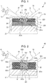
- Fig. 1 schematically illustrates a structure of a light source 10 according to a first embodiment of the present disclosure.
- the light source 10 at least includes a semiconductor light-emitting element 11 and a wavelength conversion member 20.
- the semiconductor light-emitting element 11 emits excitation light 31.
- the wavelength conversion member 20 receives the excitation light 31 and emits first light 32 having longer wavelengths than the excitation light 31 and diffusively reflected light 33 of the excitation light 31.
- the first light 32 is fluorescence or phosphorescence.
- the semiconductor light-emitting element 11 may be formed of a light-emitting diode (LED), a superluminescent diode (SLD), a laser diode (LD), or the like.
- the semiconductor light-emitting element 11 in this embodiment is an LD.
- the semiconductor light-emitting element 11 may be formed of a single LD or a plurality of LD's optically coupled.
- the semiconductor light-emitting element 11 emits, for example, blue light.
- the blue light used in the present disclosure indicates light having a peak wavelength of 420 nm or more and 470 nm or less.
- the light source 10 further includes an entrance optical system 12 that may be located in an optical path of the excitation light 31 emitted from the semiconductor light-emitting element 11.
- the entrance optical system 12 includes, for example, a lens, a mirror, an optical fiber, or any combination thereof.
- the wavelength conversion member 20 includes a surface on which excitation light from the semiconductor light-emitting element 11 is incident, and emits the first light 32 having longer wavelengths than the excitation light 31 from the surface and the diffusively reflected light 33 having the same wavelength as the excitation light 31 that has not been subjected to wavelength conversion.
- the wavelength conversion member 20 includes a first wavelength conversion layer 201 located on at least a substrate 21 and a second wavelength conversion layer 202 on the first wavelength conversion layer 201.
- the wavelength conversion member 20 further includes a reflective layer 203 located on the first wavelength conversion layer 201 and around the second wavelength conversion layer 202.
- the first wavelength conversion layer 201 includes a first main surface 201 a and a second main surface 201 b.
- the first main surface 201 a faces the substrate 21.
- the second main surface 201 b is located opposite the first main surface 201a.
- the first wavelength conversion layer 201 at least contains a first phosphor 25 and a first matrix 22.
- the first phosphor 25 has a main function of partially converting the excitation light 31 into the first light 32.
- the material composition of the first phosphor 25 is not particularly limited.
- the first phosphor 25 in this embodiment is an (Y 1-y Gd y ) 3 (Al 1-z Ga z ) 5 O 12 :Ce 3+ [0 ⁇ y ⁇ 1, 0 ⁇ z ⁇ 1] phosphor.
- the first matrix 22 may be a transparent inorganic material, for example, glass, a silicone resin, an organic-inorganic hybrid material, Al 2 O 3 , or ZnO.
- the first phosphor 25 may be sealed by, for example, the following method: (1) ZnO seed crystals are formed on the substrate 21 by vacuum deposition, and a layer consisting of only the first phosphor 25 is formed by, for example, a casting method on the ZnO seed crystals; (2) the substrate 21 with the seed crystals and the layer consisting of the first phosphor 25 is immersed in, for example, an aqueous zinc nitrate (Zn(NO 3 ) 2 solution containing hexamethylenetetramine (C 6 H 12 N 4 ); and (3) the temperature of the aqueous solution is set to 80°C. Thereby, ZnO is formed by liquid-phase deposition so as to surround the first phosphor 25.
- the ZnO serving as the first matrix 22 formed by this method has a thermal conductivity of 10 W/m ⁇ K.
- the volume ratio of the first phosphor 25 in the first wavelength conversion layer 201 is preferably 30% or more and 80% or less.
- the "volume ratio of X in Y" in the present disclosure means the percentage of the volume of X, as compared to the volume of Y, which is taken as 100%.
- the volume ratio of the first phosphor 25 in the first wavelength conversion layer 201 is 60% in this embodiment.
- heat generated during the wavelength conversion is sufficiently dissipated to the substrate 21 to inhibit an increase in the temperature of the wavelength conversion member 20, thereby inhibiting a reduction in luminous efficiency.
- the volume ratio of the first phosphor 25 in the first wavelength conversion layer 201 is 80% or less, the breaking or the like of the particles of the first phosphor 25 is inhibited.
- a reduction in luminous efficiency due to defects caused by the break is inhibited.
- the phosphor is uniformly present in the wavelength conversion layer without regularity.
- the volume ratio of the phosphor in the wavelength conversion layer is substantially the same as the proportion of the cross-sectional area of the phosphor with respect to the cross-sectional area of the entire wavelength conversion layer in a cross section of the wavelength conversion layer.
- the proportion of the cross-sectional area is used for a method of measuring the volume ratio of a phosphor in a wavelength conversion layer.
- CP processing cross-section polisher processing
- SEM scanning electron microscope
- the first wavelength conversion layer 201 may contain inorganic particles, for example, SiO 2 , Al 2 O 3 , or MgO, in a proportion lower than the volume ratio of the first phosphor 25, in addition to the first phosphor 25 and the first matrix 22. In this case, the scattering of the excitation light 31 and the first light 32 can be controlled.
- inorganic particles for example, SiO 2 , Al 2 O 3 , or MgO
- the second wavelength conversion layer 202 includes a first main surface 202a and a second main surface 202b.
- the first main surface 202a faces the second main surface 201 b of the first wavelength conversion layer 201.
- the second main surface 202b is located opposite the first main surface 202a.
- the second main surface 202b serves as a surface of the wavelength conversion member 20 on which the excitation light 31 is incident and also serves as a surface that emits the first light 32 and the diffusively reflected light 33.
- the first main surface 202a of the second wavelength conversion layer 202 lies on the side of the substrate 21.
- the second main surface 202b of the second wavelength conversion layer 202 lies on the opposite side of the substrate 21.
- the second wavelength conversion layer 202 at least includes a second phosphor 26, first inorganic particles 27, and a second matrix 23.
- the second phosphor 26 partially converts the excitation light 31 into the 32.
- the first inorganic particles 27 have the function of generating the diffusively reflected light 33 having the same wavelength as the excitation light 31.
- the material composition of the second phosphor 26 is not particularly limited and may be the same as that of the first phosphor 25.
- the second phosphor 26 in this embodiment is an (Y 1-y Gd y ) 3 (Al 1-z Ga z ) 5 O 12 :Ce 3+ [0 ⁇ y ⁇ 1, 0 ⁇ z ⁇ 1] phosphor.
- the material of the first inorganic particles 27 is preferably a transparent material that exhibits lower absorption of light in the visible region.
- Examples of the material of the first inorganic particles 27 may include SiO 2 , Al 2 O 3 , MgO, ZnO, TiO 2 , ZrO, Ta 2 O 5 , Nb 2 O 5 , BN, AIN, and BaSO 4 .
- the material of the first inorganic particles 27 in this embodiment is SiO 2 .
- Examples of the second matrix 23 may include transparent inorganic materials, such as glass, silicone resins, organic-inorganic hybrid materials, Al 2 O 3 , and ZnO.
- the second matrix 23 in this embodiment is a polysilsesquioxane, which is an organic-inorganic hybrid material having a siloxane bond.
- the second phosphor 26 and the first inorganic particles 27 may be sealed by, for example, the following method: (1) the polysilsesquioxane that has been dissolved in a benzyl alcohol solvent, the second phosphor 26, and the first inorganic particles 27 are mixed together into a paste-like mixture; and (2) the paste-like mixture is applied by, for example, a screen printing method to the first wavelength conversion layer 201 and thermally cured. Thereby, the second matrix 23 including the second phosphor 26 and the first inorganic particles 27 sealed therein is formed.
- the polysilsesquioxane serving as the second matrix 23 formed by this method has a thermal conductivity of 1 W/m ⁇ K.
- the volume ratio of the second phosphor 26 in the second wavelength conversion layer 202 is preferably lower than the volume ratio of the first phosphor 25 in the first wavelength conversion layer 201. More preferably, the volume ratio of the second phosphor 26 in the second wavelength conversion layer 202 is 0.1% or more and 20% or less. The volume ratio of the second phosphor 26 in the second wavelength conversion layer 202 may be, for example, 1%.
- the first wavelength conversion layer 201 converts the excitation light 31 into fluorescence or phosphorescence having longer wavelengths than the excitation light 31 and emits the fluorescence or phosphorescence.
- the second wavelength conversion layer 202 converts the excitation light 31 into fluorescence or phosphorescence having longer wavelengths than the excitation light 31 and emits the fluorescence or phosphorescence.
- the first light 32 emitted from the wavelength conversion member 20 includes the fluorescence or phosphorescence from the first wavelength conversion layer 201 and the fluorescence or phosphorescence from the second wavelength conversion layer 202.
- the second wavelength conversion layer 202 also emits the diffusively reflected light 33 having the same wavelength as the excitation light 31. It is thus possible to adjust the color of light emitted from the wavelength conversion member 20 by changing the thickness of the second wavelength conversion layer 202 to change the mixing ratio of the first light 32 to the diffusively reflected light 33.
- the volume ratio of the second phosphor 26 in the second wavelength conversion layer 202 is higher than the volume ratio of the first phosphor 25 in the first wavelength conversion layer 201, the amount of fluorescence or phosphorescence emitted from the second phosphor 26 varies significantly depending on the thickness of the second wavelength conversion layer 202 because the excitation light 31 is first incident on the second wavelength conversion layer 202.
- the color of light emitted from the wavelength conversion member 20 varies easily depending on a slight change in the thickness of the second wavelength conversion layer 202.
- the volume ratio of the first inorganic particles 27 in the second wavelength conversion layer 202 is not particularly limited and may be adjusted in response to the color of light obtained by combining the first light 32 with the diffusively reflected light 33 originating from the excitation light 31.
- the reflective layer 203 at least contains second inorganic particles 28 and a third matrix 24 and is located at least one side face 202c located between the first main surface 202a and the second main surface 202b of the second wavelength conversion layer 202.
- the reflective layer 203 in this embodiment is in contact with the side face 202c of the second wavelength conversion layer 202 and is located on the second main surface 201b of the first wavelength conversion layer 201.
- the second wavelength conversion layer 202 may have a circular shape, an elliptical shape, a triangular shape, a rectangular shape, or a polygonal shape in plan view (that is, when viewed from a direction perpendicular to the second main surface 202b).
- the second wavelength conversion layer 202 When the second wavelength conversion layer 202 has a circular shape or an elliptic shape in plan view, the second wavelength conversion layer 202 has a single side face. When the second wavelength conversion layer 202 has a triangular shape, a rectangular shape, or a polygonal shape, the second wavelength conversion layer 202 has a plurality of side faces.
- the reflective layer 203 has the function of suppressing the emission of the first light 32 from a surface other than the surface of the second wavelength conversion layer 202 on which the excitation light 31 is incident to improve the contrast between the light-emitting portion and the non-light-emitting portion.
- the term "contrast” used here indicates the ratio of the luminance of the second wavelength conversion layer 202 serving as a light-emitting portion to the luminance of the reflective layer 203 serving as a non-light-emitting portion (the luminance of the light-emitting portion/the luminance of the non-light-emitting portion).
- the material of the second inorganic particles 28 is preferably a transparent material that exhibits lower absorption of light in the visible region.
- the material of the second inorganic particles 28 may include SiO 2 , Al 2 O 3 , MgO, ZnO, TiO 2 , ZrO, Ta 2 O 5 , Nb 2 O 5 , BN, AIN, and BaSO 4 .
- the material of the second inorganic particles 28 in this embodiment is TiO 2 .
- the third matrix 24 may include transparent inorganic materials, such as glass, silicone resins, organic-inorganic hybrid materials, Al 2 O 3 , and ZnO.
- the third matrix 24 in this embodiment is a silicone resin having a siloxane bond.
- the second inorganic particles 28 may be sealed by, for example, the following method: (1) the polysilsesquioxane that has been dissolved in a benzyl alcohol solvent and the second inorganic particles 28 are mixed together into a paste-like mixture; and (2) the paste-like mixture is applied by, for example, a screen printing method to the first wavelength conversion layer 201 and thermally cured. Thereby, the third matrix 24 including the second inorganic particles 28 sealed therein is formed.
- the volume ratio of the first phosphor 25 in the first wavelength conversion layer 201 is higher than the volume ratio of the second phosphor 26 in the second wavelength conversion layer 202 in the first embodiment of the present disclosure as described above.
- a main source of heat generated in the wavelength conversion member 20 during wavelength conversion is the first wavelength conversion layer 201.
- the contact area among particles of the first phosphor 25 in the first wavelength conversion layer 201 is larger than the contact area among particles of the second phosphor 26 in the second wavelength conversion layer 202.
- the first wavelength conversion layer 201 is in contact with the substrate 21. This enables efficient dissipation of heat generated during wavelength conversion, thereby suppressing a reduction in luminous efficiency.
- the volume ratio of the second phosphor 26 in the second wavelength conversion layer 202 is lower than the volume ratio of the first phosphor 25 in the first wavelength conversion layer 201.
- the second wavelength conversion layer 202 contains the first inorganic particles 27.
- the ratio of the first light 32 to the diffusively reflected light 33 originating from the excitation light 31 varies depending on the thickness of the second wavelength conversion layer 202. This enables control of the color of light emitted.
- the reflective layer 203 suppresses the emission of the first light 32 from a surface other than the surface of the second wavelength conversion layer 202 on which the excitation light 31 is incident, thereby improving the contrast between the light-emitting portion and the non-light-emitting portion.
- Fig. 2 schematically illustrates a structure of a light source 40 according to a second embodiment.
- the light source 40 at least includes a semiconductor light-emitting element 41 and a wavelength conversion member 50.
- the semiconductor light-emitting element 41 emits excitation light 61.
- the wavelength conversion member 50 receives the excitation light 61 and emits first light 62 having longer wavelengths than the excitation light 61.
- the first light 62 is fluorescence or phosphorescence.
- the semiconductor light-emitting element 41 may be formed of an LED, a superluminescent diode (SLD), a laser diode (LD), or the like.
- the semiconductor light-emitting element 41 in this embodiment is an LD.
- the semiconductor light-emitting element 41 may be formed of a single LD or a plurality of LD's optically coupled.
- the semiconductor light-emitting element 41 emits, for example, blue light.
- the light source 40 further includes an entrance optical system 42 that may be located in an optical path of the excitation light 61 emitted from the semiconductor light-emitting element 41.
- the entrance optical system 42 includes, for example, a lens, a mirror, an optical fiber, or any combination thereof.
- the wavelength conversion member 50 includes a surface on which excitation light from the semiconductor light-emitting element 41 is incident, and emits the first light 62 having longer wavelengths than the excitation light 61 from the surface and diffusively reflected light 63 having the same wavelength as the excitation light 61 that has not been subjected to wavelength conversion.
- the wavelength conversion member 50 includes a first wavelength conversion layer 501 located on at least a substrate 51 and a second wavelength conversion layer 502 on the first wavelength conversion layer 501.
- the wavelength conversion member 50 further includes a reflective layer 503 located on a side face of the first wavelength conversion layer 501 and a side face of the second wavelength conversion layer 502.
- the first wavelength conversion layer 501 includes a first main surface 501 a, a second main surface 501b, and at least one side face 501 c located between the first main surface 501 a and the second main surface 501 b.
- the first main surface 501a faces the substrate 51.
- the second main surface 501b is located opposite the first main surface 501a.
- the first wavelength conversion layer 501 at least contains a first phosphor 55 and a first matrix 52.
- the first wavelength conversion layer 501 has a main function of converting the excitation light 61 into the first light 62.
- the material composition of the first phosphor 55 is not particularly limited.
- the first phosphor 55 in this embodiment is an (Y 1-y Gd y ) 3 (Al 1-z Ga z ) 5 O 12 :Ce 3+ [0 ⁇ y ⁇ 1,0 ⁇ z ⁇ 1] phosphor.
- the first matrix 52 may be a transparent inorganic material, for example, glass, a silicone resin, an organic-inorganic hybrid material, Al 2 O 3 , or ZnO.
- the first matrix 52 in this embodiment is ZnO.
- the first phosphor 55 may be sealed by, for example, the following method: (1) ZnO seed crystals are formed by vacuum deposition on a portion of the substrate 51 where the first wavelength conversion layer 501 is to be formed, and then a layer consisting of the first phosphor 55 is formed by a casting method on the ZnO seed crystals; (2) the substrate 51 with the seed crystals and the layer consisting of the first phosphor 55 is immersed in an aqueous zinc nitrate (Zn(NO 3 ) 2 solution containing hexamethylenetetramine (C 6 H 12 N 4 ); and (3) the temperature of the aqueous solution is set to 80°C.
- Zn(NO 3 ) 2 solution containing hexamethylenetetramine (C 6 H 12 N 4 )
- ZnO is formed by liquid-phase deposition on a specific portion of the substrate 51 so as to surround the first phosphor 55 to form the first wavelength conversion layer 501.
- the ZnO serving as the first matrix 52 formed by this method has a thermal conductivity of 10 W/m ⁇ K.
- the volume ratio of the first phosphor 55 in the first wavelength conversion layer 501 is 30% or more and 80% or less.
- the volume ratio of the first phosphor 55 in the first wavelength conversion layer 501 is 50% in this embodiment.
- the contact area among particles of the first phosphor 55 is large, so that thermal conduction between the particles occurs easily.
- heat generated during the wavelength conversion is sufficiently dissipated to the substrate 51 to inhibit an increase in the temperature of the wavelength conversion member 50, thereby inhibiting a reduction in luminous efficiency.
- the volume ratio of the first phosphor 55 in the first wavelength conversion layer 501 is 80% or less, the breaking or the like of the particles of the first phosphor 55 is inhibited. Thus, a reduction in luminous efficiency due to defects caused by the break is inhibited.
- the first wavelength conversion layer 501 may contain inorganic particles, for example, SiO 2 , Al 2 O 3 , or MgO, in a proportion lower than the volume ratio of the first phosphor 55, in addition to the first phosphor 55 and the first matrix 52. In this case, the scattering of the excitation light 61 and the first light 62 can be controlled.
- inorganic particles for example, SiO 2 , Al 2 O 3 , or MgO
- the second wavelength conversion layer 502 includes a first main surface 502a, a second main surface 502b, and at least one side face 502c located between the first main surface 502a and the second main surface 502b.
- the first main surface 502a faces the second main surface 501 b of the first wavelength conversion layer 501.
- the second main surface 502b is located opposite the first main surface 502a.
- the second wavelength conversion layer 502 at least contains a second phosphor 56, first inorganic particles 57, and a second matrix 53.
- the second phosphor 56 partially converts the excitation light 61 into the first light 62.
- the first inorganic particles 57 have a function of generating the diffusively reflected light 63 having the same wavelength as the excitation light 61.
- the material composition of the second phosphor 56 is not particularly limited and may be a different composition from that of the first phosphor 55.
- the second phosphor 56 in this embodiment is a (Sr s ,Ca t )AlSiN:Eu 2+ [0 ⁇ s ⁇ 1, 0 ⁇ t ⁇ 1] phosphor.
- the material of the first inorganic particles 57 is preferably a transparent material that exhibits lower absorption of light in the visible region. Examples of the material of the first inorganic particles 57 may include SiO 2 , Al 2 O 3 , MgO, ZnO, TiO 2 , ZrO, Ta 2 O 5 , Nb 2 O 5 , BN, AIN, and BaSO 4 .
- the material of the first inorganic particles 57 in this embodiment is SiO 2 .
- the second matrix 53 may include transparent inorganic materials, such as glass, silicone resins, organic-inorganic hybrid materials, Al 2 O 3 , and ZnO.
- the second matrix 53 in this embodiment is a polysilsesquioxane, which is an organic-inorganic hybrid material having a siloxane bond.
- the second phosphor 56 and the first inorganic particles 57 may be sealed by, for example, the following method: (1) the polysilsesquioxane that has been dissolved in a benzyl alcohol solvent, the second phosphor 56, and the first inorganic particles 57 are mixed together into a paste-like mixture; and (2) the paste-like mixture is applied by, for example, a screen printing method to the first wavelength conversion layer 501 and thermally cured. Thereby, the second matrix 53 including the second phosphor 56 and the first inorganic particles 57 sealed therein is formed.
- the polysilsesquioxane serving as the second matrix 53 formed by this method has a thermal conductivity of 1 W/m ⁇ K.
- the volume ratio of the second phosphor 56 in the second wavelength conversion layer 502 is preferably lower than that of the first phosphor 55 in the first wavelength conversion layer 501. More preferably, the volume ratio of the second phosphor 56 in the second wavelength conversion layer 502 is 0.1% or more and 20% or less. The volume ratio of the second phosphor 56 in the second wavelength conversion layer 502 may be, for example, 10%.
- the first wavelength conversion layer 501 converts the excitation light 61 into fluorescence or phosphorescence having longer wavelengths than the excitation light 61 and emits the fluorescence or phosphorescence.
- the second wavelength conversion layer 502 converts the excitation light 61 into fluorescence or phosphorescence having longer wavelengths than the excitation light 61 and emits the fluorescence or phosphorescence.
- the first light 62 emitted from the wavelength conversion member 50 includes the fluorescence or phosphorescence from the first wavelength conversion layer 501 and the fluorescence or phosphorescence from the second wavelength conversion layer 502.
- the second wavelength conversion layer 502 also emits the diffusively reflected light 63 having the same wavelength as the excitation light 61. It is thus possible to adjust the color of light emitted from the wavelength conversion member 50 by changing the thickness of the second wavelength conversion layer 502 to change the mixing ratio of the first light 62 to the diffusively reflected light 63.
- the amount of the first light 62 emitted from the second phosphor 56 varies significantly depending on the thickness of the second wavelength conversion layer 502 because the excitation light 61 is first incident on the second wavelength conversion layer 502.
- the color of light emitted from the wavelength conversion member 50 varies easily depending on a slight change in the thickness of the second wavelength conversion layer 502.
- the volume ratio of the first inorganic particles 57 in the second wavelength conversion layer 502 is not particularly limited and may be adjusted in response to the color of light obtained by combining the first light 62 with the diffusively reflected light 63 originating from the excitation light 61.
- the reflective layer 503 at least contains second inorganic particles 58 and a third matrix 54 and is located on the side face 501c of the first wavelength conversion layer 501 and the side face 502c of the second wavelength conversion layer 502.
- the reflective layer 503 in this embodiment is in contact with the side face 501 c of the first wavelength conversion layer 501 and the side face 502c of the second wavelength conversion layer 502 and is located on the substrate 51.
- Each of the first wavelength conversion layer 501 and the second wavelength conversion layer 502 may have a circular shape, an elliptical shape, a triangular shape, a rectangular shape, or a polygonal shape in plan view (that is, when viewed from a direction perpendicular to the second main surface 502b).
- each of the first wavelength conversion layer 501 and the second wavelength conversion layer 502 has a circular shape or an elliptic shape in plan view, each has a single side face.
- each of the first wavelength conversion layer 501 and the second wavelength conversion layer 502 has a triangular shape, a rectangular shape, or a polygonal shape, each has a plurality of side faces.
- the shape of the first wavelength conversion layer 501 and the shape of the second wavelength conversion layer 502 in plan view may be the same or different.
- the reflective layer 503 has a function of suppressing the emission of the first light 62 from a surface other than the surface of the second wavelength conversion layer 502 on which the excitation light 61 is incident to improve the contrast between the light-emitting portion and the non-light-emitting portion.
- the material of the second inorganic particles 58 is preferably a transparent material that exhibits lower absorption of light in the visible region. Examples of the material of the second inorganic particles 58 may include SiO 2 , Al 2 O 3 , MgO, ZnO, TiO 2 , ZrO, Ta 2 O 5 , Nb 2 O 5 , BN, AIN, and BaSO 4 . For example, the material of the second inorganic particles 58 in this embodiment is TiO 2 .
- the third matrix 54 may include transparent inorganic materials, such as glass, silicone resins, organic-inorganic hybrid materials, Al 2 O 3 , and ZnO.
- the third matrix 54 in this embodiment is a silicone resin having a siloxane bond.
- the second inorganic particles 58 may be sealed by, for example, the following method: (1) the uncured silicone resin and the second inorganic particles 58 are mixed together into a paste-like mixture; and (2) the paste-like mixture is applied by, for example, a screen printing method only to the substrate 51 and thermally cured. Thereby, the third matrix 54 including the second inorganic particles 58 sealed therein is formed.
- the volume ratio of the first phosphor 55 in the first wavelength conversion layer 501 is higher than the volume ratio of the second phosphor 56 in the second wavelength conversion layer 502 in the second embodiment of the present disclosure as described above.
- a main source of heat generated in the wavelength conversion member 50 during wavelength conversion is the first wavelength conversion layer 501.
- the contact area among particles of the first phosphor 55 in the first wavelength conversion layer 501 is larger than the contact area among particles of the second phosphor 56 in the second wavelength conversion layer 502.
- the first wavelength conversion layer 501 is in contact with the substrate 51. This enables efficient dissipation of heat generated during wavelength conversion, thereby suppressing a reduction in luminous efficiency.
- the volume ratio of the second phosphor 56 in the second wavelength conversion layer 502 is lower than the volume ratio of the first phosphor 55 in the first wavelength conversion layer 501.
- the second wavelength conversion layer 502 contains the first inorganic particles 57.
- the ratio of the first light 62 to the diffusively reflected light 63 originating from the excitation light 61 varies depending on the thickness of the second wavelength conversion layer 502. This enables easy control of the color of light emitted.
- the first phosphor 55 and the second phosphor 56 have different material compositions in the second embodiment of the present disclosure.
- the reflective layer 503 suppresses the emission of the first light 62 from a surface other than the surface of the second wavelength conversion layer 502 on which the excitation light 61 is incident to improve the contrast between the light-emitting portion and the non-light-emitting portion.
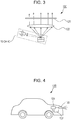
- Fig. 3 schematically illustrates a structure of a vehicle headlamp 120 according to a third embodiment of the present disclosure.
- the vehicle headlamp 120 in this embodiment includes the light source 10 in the first embodiment or the light source 40 in the second embodiment; and an exit optical system 122 that guides light from the light source toward the front.
- a wavelength cutoff filter 121 that partially absorbs or reflects light from the light source may be provided.
- the exit optical system 122 guides light from the light source 10 or the light source 40 to the outside.
- the exit optical system 122 is, for example, a projection lens.
- the vehicle headlamp 120 may be what is called a projector-type vehicle headlamp or a reflector-type vehicle headlamp.
- vehicle used in the present disclosure includes automobiles, two-wheeled vehicles, and special-purpose vehicles.
- the vehicle headlamp according to the third embodiment provides the same advantageous effects as those obtained in the first or second embodiment.
- the vehicle headlamp 120 emits a high-contrast light beam even when the state of collection of light emitted from the light source 10 or 40 is adjusted with the projection lens because of the improved contrast between the light-emitting portion an the non-light-emitting portion of the light source 10 or 40.
- Fig. 4 schematically illustrates a structure of a vehicle 130 according to a fourth embodiment of the present disclosure.
- the vehicle 130 includes the vehicle headlamp 120 according to the third embodiment and a power supply source 131.
- the vehicle 130 may include a generator 132 that is rotationally driven by a driving source such as an engine to generate electric power.
- the electric power generated by the generator 132 is stored in the power supply source 131.
- the power supply source 131 is, for example, a secondary battery that can be charged and discharged.
- the vehicle headlamp 120 is operated by electric power from the power supply source 131.
- Examples of the vehicle 130 include automobiles, two-wheeled vehicles, and special-purpose vehicles.
- the vehicle 130 may be an engined vehicle, an electric vehicle, or a hybrid electric vehicle.
- the vehicle according to the fourth embodiment also provides the same advantageous effects as those obtained in the first or second embodiment.
- the wavelength conversion member according to an embodiment of the present disclosure is usable for light sources, such as special lighting devices, head-up displays, projectors, and vehicle headlamps.
Landscapes
- Chemical & Material Sciences (AREA)
- Engineering & Computer Science (AREA)
- Materials Engineering (AREA)
- Organic Chemistry (AREA)
- Inorganic Chemistry (AREA)
- General Engineering & Computer Science (AREA)
- Physics & Mathematics (AREA)
- Optics & Photonics (AREA)
- Mechanical Engineering (AREA)
- Optical Filters (AREA)
- Non-Portable Lighting Devices Or Systems Thereof (AREA)
- Led Device Packages (AREA)
- Semiconductor Lasers (AREA)
Applications Claiming Priority (1)
| Application Number | Priority Date | Filing Date | Title |
|---|---|---|---|
| JP2016084523 | 2016-04-20 |
Publications (1)
| Publication Number | Publication Date |
|---|---|
| EP3236136A1 true EP3236136A1 (fr) | 2017-10-25 |
Family
ID=58488886
Family Applications (1)
| Application Number | Title | Priority Date | Filing Date |
|---|---|---|---|
| EP17164498.2A Withdrawn EP3236136A1 (fr) | 2016-04-20 | 2017-04-03 | Élément de conversion de longueur d'onde comprenant un luminophore convertissant la lumière d'un élément électroluminescent à semi-conducteur en lumière de longueur d'onde plus longue |
Country Status (4)
| Country | Link |
|---|---|
| US (1) | US10094529B2 (fr) |
| EP (1) | EP3236136A1 (fr) |
| JP (1) | JP2017198982A (fr) |
| CN (1) | CN107305921A (fr) |
Cited By (1)
| Publication number | Priority date | Publication date | Assignee | Title |
|---|---|---|---|---|
| CN109751563A (zh) * | 2017-11-03 | 2019-05-14 | Lg电子株式会社 | 荧光体模块 |
Families Citing this family (15)
| Publication number | Priority date | Publication date | Assignee | Title |
|---|---|---|---|---|
| EP3367141B1 (fr) | 2015-10-20 | 2020-12-16 | Panasonic Semiconductor Solutions Co., Ltd. | Élément de conversion de longueur d'onde et dispositif électroluminescent |
| JPWO2017169628A1 (ja) * | 2016-03-30 | 2019-02-28 | ソニー株式会社 | 発光素子および光源装置ならびに投射型表示装置 |
| EP3480863B1 (fr) * | 2016-07-04 | 2021-05-19 | Panasonic Intellectual Property Management Co., Ltd. | Dispositif électroluminescent utilisant du fluorophore |
| KR20190028628A (ko) | 2016-07-04 | 2019-03-19 | 파나소닉 아이피 매니지먼트 가부시키가이샤 | 형광체 및 발광 장치 |
| WO2018008283A1 (fr) | 2016-07-04 | 2018-01-11 | パナソニックIpマネジメント株式会社 | Source lumineuse à fibre, endoscope et système endoscopique |
| WO2018008284A1 (fr) | 2016-07-04 | 2018-01-11 | パナソニックIpマネジメント株式会社 | Dispositif de projecteur |
| JP6919434B2 (ja) * | 2017-09-06 | 2021-08-18 | セイコーエプソン株式会社 | 波長変換素子、光源装置およびプロジェクター |
| JP2019109330A (ja) * | 2017-12-18 | 2019-07-04 | パナソニックIpマネジメント株式会社 | 波長変換デバイス、光源装置、照明装置、及び、投写型映像表示装置 |
| CN110361912B (zh) * | 2018-04-10 | 2021-08-17 | 深圳光峰科技股份有限公司 | 波长转换装置 |
| WO2019203078A1 (fr) * | 2018-04-19 | 2019-10-24 | パナソニックIpマネジメント株式会社 | Dispositif électroluminescent |
| JP7113277B2 (ja) * | 2018-09-12 | 2022-08-05 | パナソニックIpマネジメント株式会社 | 波長変換部材及びそれを用いた光源装置、プロジェクタならびに車両 |
| WO2020129358A1 (fr) * | 2018-12-18 | 2020-06-25 | パナソニックIpマネジメント株式会社 | Élément de conversion de longueur d'onde, dispositif optique et projecteur |
| DE102019121511A1 (de) * | 2019-08-09 | 2021-02-11 | Schott Ag | Lichtkonversions- und Beleuchtungseinrichtung |
| JP7429346B2 (ja) * | 2019-10-03 | 2024-02-08 | 国立研究開発法人物質・材料研究機構 | 波長変換部材 |
| CN113671780A (zh) * | 2021-08-31 | 2021-11-19 | 青岛海信激光显示股份有限公司 | 发光单元、光源系统和激光投影设备 |
Citations (6)
| Publication number | Priority date | Publication date | Assignee | Title |
|---|---|---|---|---|
| JP2012099280A (ja) | 2010-10-29 | 2012-05-24 | Sharp Corp | 発光装置、車両用前照灯および照明装置 |
| US20140072812A1 (en) * | 2012-05-22 | 2014-03-13 | Panasonic Corporation | Wavelength conversion element including phosphor particles, and led element and semiconductor laser light emitting device using wavelength conversion element |
| US20140369064A1 (en) * | 2013-06-18 | 2014-12-18 | Sharp Kabushiki Kaisha | Light-emitting device |
| US20150184830A1 (en) * | 2013-06-21 | 2015-07-02 | Panasonic Intellectual Property Management Co., Ltd. | Wavelength conversion member, light source, and vehicle head lamp |
| US20150252964A1 (en) * | 2014-03-05 | 2015-09-10 | Sharp Kabushiki Kaisha | Light source device and illumination apparatus |
| JP2016027613A (ja) * | 2014-05-21 | 2016-02-18 | 日本電気硝子株式会社 | 波長変換部材及びそれを用いた発光装置 |
Family Cites Families (19)
| Publication number | Priority date | Publication date | Assignee | Title |
|---|---|---|---|---|
| TW200950149A (en) * | 2008-01-15 | 2009-12-01 | Goeken Group Corp | Silicon nanoparticle white light emitting diode device |
| US8410679B2 (en) * | 2010-09-21 | 2013-04-02 | Cree, Inc. | Semiconductor light emitting devices with densely packed phosphor layer at light emitting surface |
| US8610341B2 (en) * | 2010-10-05 | 2013-12-17 | Intematix Corporation | Wavelength conversion component |
| JP2012089316A (ja) | 2010-10-19 | 2012-05-10 | Stanley Electric Co Ltd | 光源装置および照明装置 |
| DE102011078689A1 (de) * | 2011-07-05 | 2013-01-10 | Osram Ag | Verfahren zur Herstellung eines Konversionselements und Konversionselement |
| US9046228B2 (en) * | 2012-04-06 | 2015-06-02 | Panasonic Intellectual Property Management Co., Ltd. | Light-emitting device for emitting light of multiple color temperatures |
| JP6132204B2 (ja) | 2012-05-16 | 2017-05-24 | パナソニックIpマネジメント株式会社 | 波長変換素子およびその製造方法ならびに波長変換素子を用いたled素子および半導体レーザ発光装置 |
| DE102012107290A1 (de) * | 2012-08-08 | 2014-02-13 | Osram Opto Semiconductors Gmbh | Optoelektronisches Halbleiterbauteil, Konversionsmittelplättchen und Verfahren zur Herstellung eines Konversionsmittelplättchens |
| EP2940101B1 (fr) * | 2012-12-28 | 2020-03-11 | Shin-Etsu Chemical Co., Ltd. | Corps moulé de résine contenant un luminophore, dispositif électroluminescent et pastille de résine |
| CN104100933B (zh) * | 2013-04-04 | 2016-08-10 | 深圳市绎立锐光科技开发有限公司 | 一种波长转换装置及其制作方法、相关发光装置 |
| JP2015005650A (ja) | 2013-06-21 | 2015-01-08 | パナソニック株式会社 | 波長変換部材、波長変換部材を具備する光源、及び光源を具備する車両用ヘッドランプ |
| US9142733B2 (en) * | 2013-09-03 | 2015-09-22 | Panasonic Intellectual Property Management Co., Ltd. | Light source device including a high energy light source and a wavelength conversion member, illuminating device comprising the same, and vehicle |
| JP2015050124A (ja) | 2013-09-03 | 2015-03-16 | スタンレー電気株式会社 | 発光装置 |
| JP5935067B2 (ja) | 2013-10-10 | 2016-06-15 | パナソニックIpマネジメント株式会社 | 波長変換板、およびそれを用いた照明装置 |
| CN103647013A (zh) * | 2013-10-28 | 2014-03-19 | 吴震 | 波长转换装置的制造方法和发光装置 |
| KR102075993B1 (ko) * | 2013-12-23 | 2020-02-11 | 삼성전자주식회사 | 백색 led 소자들을 제조하는 방법 |
| JP2015144261A (ja) * | 2013-12-26 | 2015-08-06 | インテマティックス・コーポレーションIntematix Corporation | フォトルミネセンス波長変換を用いる固体発光デバイス |
| CN107304984B (zh) * | 2016-04-22 | 2020-06-09 | 松下电器产业株式会社 | 波长转换部件以及投光灯 |
| CN110556464A (zh) * | 2018-06-01 | 2019-12-10 | 深圳市绎立锐光科技开发有限公司 | 发光二极管封装结构及封装方法 |
-
2017
- 2017-03-08 CN CN201710134584.5A patent/CN107305921A/zh active Pending
- 2017-03-24 US US15/468,183 patent/US10094529B2/en active Active
- 2017-04-03 EP EP17164498.2A patent/EP3236136A1/fr not_active Withdrawn
- 2017-04-11 JP JP2017078471A patent/JP2017198982A/ja active Pending
Patent Citations (7)
| Publication number | Priority date | Publication date | Assignee | Title |
|---|---|---|---|---|
| JP2012099280A (ja) | 2010-10-29 | 2012-05-24 | Sharp Corp | 発光装置、車両用前照灯および照明装置 |
| US20140072812A1 (en) * | 2012-05-22 | 2014-03-13 | Panasonic Corporation | Wavelength conversion element including phosphor particles, and led element and semiconductor laser light emitting device using wavelength conversion element |
| US20140369064A1 (en) * | 2013-06-18 | 2014-12-18 | Sharp Kabushiki Kaisha | Light-emitting device |
| US20150184830A1 (en) * | 2013-06-21 | 2015-07-02 | Panasonic Intellectual Property Management Co., Ltd. | Wavelength conversion member, light source, and vehicle head lamp |
| US20150252964A1 (en) * | 2014-03-05 | 2015-09-10 | Sharp Kabushiki Kaisha | Light source device and illumination apparatus |
| JP2016027613A (ja) * | 2014-05-21 | 2016-02-18 | 日本電気硝子株式会社 | 波長変換部材及びそれを用いた発光装置 |
| EP3147955A1 (fr) * | 2014-05-21 | 2017-03-29 | Nippon Electric Glass Co., Ltd. | Organe de conversion de longueur d'onde et dispositif électroluminescent l'utilisant |
Cited By (2)
| Publication number | Priority date | Publication date | Assignee | Title |
|---|---|---|---|---|
| CN109751563A (zh) * | 2017-11-03 | 2019-05-14 | Lg电子株式会社 | 荧光体模块 |
| US11067242B2 (en) | 2017-11-03 | 2021-07-20 | Lg Electronics Inc. | Phosphor module |
Also Published As
| Publication number | Publication date |
|---|---|
| JP2017198982A (ja) | 2017-11-02 |
| US20170307163A1 (en) | 2017-10-26 |
| CN107305921A (zh) | 2017-10-31 |
| US10094529B2 (en) | 2018-10-09 |
Similar Documents
| Publication | Publication Date | Title |
|---|---|---|
| US10094529B2 (en) | Wavelength conversion member including phosphor that converts light from semiconductor light-emitting element into longer-wavelength light | |
| US9785039B2 (en) | Wavelength conversion member, light emitting device, projector, and method of manufacturing wavelength conversion member | |
| JP5232815B2 (ja) | 車両用前照灯 | |
| US9142733B2 (en) | Light source device including a high energy light source and a wavelength conversion member, illuminating device comprising the same, and vehicle | |
| US7356054B2 (en) | Light emitting device | |
| US10365551B2 (en) | Wavelength conversion member including phosphor | |
| CN102798085B (zh) | 光源装置以及照明装置 | |
| US20140003074A1 (en) | Wavelength conversion member and method for manufacturing the same, and light-emitting device, illuminating device, and headlight | |
| JP5172987B2 (ja) | 発光装置、照明装置および前照灯 | |
| US11946606B2 (en) | Wavelength conversion member, light source device using same, projector and vehicle | |
| JP5053416B2 (ja) | 発光装置、照明装置および車両用前照灯 | |
| JP2012099282A (ja) | 照明装置及び車両用前照灯 | |
| US20110216554A1 (en) | Light emitting device | |
| US20140016300A1 (en) | Light emitting device, illuminating apparatus, and light emitting method | |
| JP5624384B2 (ja) | 発光装置、照明装置および車両用前照灯 | |
| JP2012193283A (ja) | 発光体、発光装置、照明装置および前照灯 | |
| WO2013051623A1 (fr) | Corps émetteur de lumière, dispositif d'éclairage et phare | |
| US20190032866A1 (en) | Light emitting device and illuminating apparatus | |
| JP5271340B2 (ja) | 発光装置、照明装置および車両用前照灯 | |
| JP2012221633A (ja) | 照明装置及び前照灯 | |
| JP5557883B2 (ja) | 発光装置、照明装置、車両用前照灯 | |
| US11111385B2 (en) | Silicone composition | |
| US11105482B2 (en) | Light source device, projector, and vehicle | |
| JP2014239080A (ja) | 発光装置、照明装置および車両用前照灯 | |
| JP2012119121A (ja) | 光源装置および照明装置 |
Legal Events
| Date | Code | Title | Description |
|---|---|---|---|
| PUAI | Public reference made under article 153(3) epc to a published international application that has entered the european phase |
Free format text: ORIGINAL CODE: 0009012 |
|
| AK | Designated contracting states |
Kind code of ref document: A1 Designated state(s): AL AT BE BG CH CY CZ DE DK EE ES FI FR GB GR HR HU IE IS IT LI LT LU LV MC MK MT NL NO PL PT RO RS SE SI SK SM TR |
|
| AX | Request for extension of the european patent |
Extension state: BA ME |
|
| STAA | Information on the status of an ep patent application or granted ep patent |
Free format text: STATUS: REQUEST FOR EXAMINATION WAS MADE |
|
| 17P | Request for examination filed |
Effective date: 20180411 |
|
| RBV | Designated contracting states (corrected) |
Designated state(s): AL AT BE BG CH CY CZ DE DK EE ES FI FR GB GR HR HU IE IS IT LI LT LU LV MC MK MT NL NO PL PT RO RS SE SI SK SM TR |
|
| STAA | Information on the status of an ep patent application or granted ep patent |
Free format text: STATUS: THE APPLICATION HAS BEEN WITHDRAWN |
|
| 18W | Application withdrawn |
Effective date: 20210311 |