EP3249683B1 - Verfahren zur herstellung eines halbleitersubstrats mit hohem widerstand - Google Patents
Verfahren zur herstellung eines halbleitersubstrats mit hohem widerstand Download PDFInfo
- Publication number
- EP3249683B1 EP3249683B1 EP17171861.2A EP17171861A EP3249683B1 EP 3249683 B1 EP3249683 B1 EP 3249683B1 EP 17171861 A EP17171861 A EP 17171861A EP 3249683 B1 EP3249683 B1 EP 3249683B1
- Authority
- EP
- European Patent Office
- Prior art keywords
- approximately
- stage
- substrate
- process according
- layer
- Prior art date
- Legal status (The legal status is an assumption and is not a legal conclusion. Google has not performed a legal analysis and makes no representation as to the accuracy of the status listed.)
- Active
Links
Images

Classifications
-
- H—ELECTRICITY
- H10—SEMICONDUCTOR DEVICES; ELECTRIC SOLID-STATE DEVICES NOT OTHERWISE PROVIDED FOR
- H10P—GENERIC PROCESSES OR APPARATUS FOR THE MANUFACTURE OR TREATMENT OF DEVICES COVERED BY CLASS H10
- H10P90/00—Preparation of wafers not covered by a single main group of this subclass, e.g. wafer reinforcement
- H10P90/19—Preparing inhomogeneous wafers
- H10P90/1904—Preparing vertically inhomogeneous wafers
- H10P90/1906—Preparing SOI wafers
-
- H—ELECTRICITY
- H10—SEMICONDUCTOR DEVICES; ELECTRIC SOLID-STATE DEVICES NOT OTHERWISE PROVIDED FOR
- H10P—GENERIC PROCESSES OR APPARATUS FOR THE MANUFACTURE OR TREATMENT OF DEVICES COVERED BY CLASS H10
- H10P90/00—Preparation of wafers not covered by a single main group of this subclass, e.g. wafer reinforcement
- H10P90/19—Preparing inhomogeneous wafers
- H10P90/1904—Preparing vertically inhomogeneous wafers
- H10P90/1906—Preparing SOI wafers
- H10P90/1914—Preparing SOI wafers using bonding
- H10P90/1916—Preparing SOI wafers using bonding with separation or delamination along an ion implanted layer, e.g. Smart-cut
-
- H—ELECTRICITY
- H10—SEMICONDUCTOR DEVICES; ELECTRIC SOLID-STATE DEVICES NOT OTHERWISE PROVIDED FOR
- H10P—GENERIC PROCESSES OR APPARATUS FOR THE MANUFACTURE OR TREATMENT OF DEVICES COVERED BY CLASS H10
- H10P32/00—Diffusion of dopants within, into or out of wafers, substrates or parts of devices
- H10P32/10—Diffusion of dopants within, into or out of semiconductor bodies or layers
- H10P32/14—Diffusion of dopants within, into or out of semiconductor bodies or layers within a single semiconductor body or layer in a solid phase; between different semiconductor bodies or layers, both in a solid phase
- H10P32/1404—Diffusion of dopants within, into or out of semiconductor bodies or layers within a single semiconductor body or layer in a solid phase; between different semiconductor bodies or layers, both in a solid phase using predeposition followed by drive-in of impurities into the semiconductor surface, e.g. predeposition from a gaseous phase
- H10P32/1406—Diffusion of dopants within, into or out of semiconductor bodies or layers within a single semiconductor body or layer in a solid phase; between different semiconductor bodies or layers, both in a solid phase using predeposition followed by drive-in of impurities into the semiconductor surface, e.g. predeposition from a gaseous phase by ion implantation
-
- H—ELECTRICITY
- H10—SEMICONDUCTOR DEVICES; ELECTRIC SOLID-STATE DEVICES NOT OTHERWISE PROVIDED FOR
- H10P—GENERIC PROCESSES OR APPARATUS FOR THE MANUFACTURE OR TREATMENT OF DEVICES COVERED BY CLASS H10
- H10P72/00—Handling or holding of wafers, substrates or devices during manufacture or treatment thereof
- H10P72/06—Apparatus for monitoring, sorting, marking, testing or measuring
- H10P72/0602—Temperature monitoring
-
- H—ELECTRICITY
- H10—SEMICONDUCTOR DEVICES; ELECTRIC SOLID-STATE DEVICES NOT OTHERWISE PROVIDED FOR
- H10P—GENERIC PROCESSES OR APPARATUS FOR THE MANUFACTURE OR TREATMENT OF DEVICES COVERED BY CLASS H10
- H10P95/00—Generic processes or apparatus for manufacture or treatments not covered by the other groups of this subclass
- H10P95/90—Thermal treatments, e.g. annealing or sintering
-
- H—ELECTRICITY
- H10—SEMICONDUCTOR DEVICES; ELECTRIC SOLID-STATE DEVICES NOT OTHERWISE PROVIDED FOR
- H10W—GENERIC PACKAGES, INTERCONNECTIONS, CONNECTORS OR OTHER CONSTRUCTIONAL DETAILS OF DEVICES COVERED BY CLASS H10
- H10W10/00—Isolation regions in semiconductor bodies between components of integrated devices
- H10W10/10—Isolation regions comprising dielectric materials
- H10W10/181—Semiconductor-on-insulator [SOI] isolation regions, e.g. buried oxide regions of SOI wafers
-
- H—ELECTRICITY
- H10—SEMICONDUCTOR DEVICES; ELECTRIC SOLID-STATE DEVICES NOT OTHERWISE PROVIDED FOR
- H10P—GENERIC PROCESSES OR APPARATUS FOR THE MANUFACTURE OR TREATMENT OF DEVICES COVERED BY CLASS H10
- H10P10/00—Bonding of wafers, substrates or parts of devices
- H10P10/12—Bonding of semiconductor wafers or semiconductor substrates to semiconductor wafers or semiconductor substrates
- H10P10/128—Bonding of semiconductor wafers or semiconductor substrates to semiconductor wafers or semiconductor substrates by direct semiconductor to semiconductor bonding
-
- H—ELECTRICITY
- H10—SEMICONDUCTOR DEVICES; ELECTRIC SOLID-STATE DEVICES NOT OTHERWISE PROVIDED FOR
- H10P—GENERIC PROCESSES OR APPARATUS FOR THE MANUFACTURE OR TREATMENT OF DEVICES COVERED BY CLASS H10
- H10P30/00—Ion implantation into wafers, substrates or parts of devices
- H10P30/20—Ion implantation into wafers, substrates or parts of devices into semiconductor materials, e.g. for doping
- H10P30/202—Ion implantation into wafers, substrates or parts of devices into semiconductor materials, e.g. for doping characterised by the semiconductor materials
- H10P30/204—Ion implantation into wafers, substrates or parts of devices into semiconductor materials, e.g. for doping characterised by the semiconductor materials into Group IV semiconductors
-
- H—ELECTRICITY
- H10—SEMICONDUCTOR DEVICES; ELECTRIC SOLID-STATE DEVICES NOT OTHERWISE PROVIDED FOR
- H10P—GENERIC PROCESSES OR APPARATUS FOR THE MANUFACTURE OR TREATMENT OF DEVICES COVERED BY CLASS H10
- H10P30/00—Ion implantation into wafers, substrates or parts of devices
- H10P30/20—Ion implantation into wafers, substrates or parts of devices into semiconductor materials, e.g. for doping
- H10P30/208—Ion implantation into wafers, substrates or parts of devices into semiconductor materials, e.g. for doping of electrically inactive species
-
- H—ELECTRICITY
- H10—SEMICONDUCTOR DEVICES; ELECTRIC SOLID-STATE DEVICES NOT OTHERWISE PROVIDED FOR
- H10P—GENERIC PROCESSES OR APPARATUS FOR THE MANUFACTURE OR TREATMENT OF DEVICES COVERED BY CLASS H10
- H10P36/00—Gettering within semiconductor bodies
- H10P36/03—Gettering within semiconductor bodies within silicon bodies
- H10P36/07—Gettering within semiconductor bodies within silicon bodies of silicon-on-insulator structures
-
- H—ELECTRICITY
- H10—SEMICONDUCTOR DEVICES; ELECTRIC SOLID-STATE DEVICES NOT OTHERWISE PROVIDED FOR
- H10P—GENERIC PROCESSES OR APPARATUS FOR THE MANUFACTURE OR TREATMENT OF DEVICES COVERED BY CLASS H10
- H10P90/00—Preparation of wafers not covered by a single main group of this subclass, e.g. wafer reinforcement
- H10P90/19—Preparing inhomogeneous wafers
- H10P90/1904—Preparing vertically inhomogeneous wafers
- H10P90/1906—Preparing SOI wafers
- H10P90/1914—Preparing SOI wafers using bonding
Definitions
- the present invention relates to a process for the manufacture of a high resistivity semiconductor substrate by layer transfer and relates in particular to the improvement in the substrates of the silicon-on-insulator type having a high resistivity and having a high concentration of interstitial oxygen.
- high resistivity is understood to mean approximately 750 ⁇ m or more and “high concentration of interstitial oxygen” is understood to mean approximately 25 ppma or more, i.e. approximately 12.5 ⁇ 10 17 atoms ⁇ cm -3 or more.
- the abovementioned stabilization stage is conventionally carried out during the stage of sacrificial oxidation of the SOI following a layer transfer carried out, for example, by the known SmartCut ® technique.
- the stabilization stage is more particularly carried out after a smoothing annealing subsequent to the layer transfer, which is generally a rapid annealing, i.e. RTA ("Rapid Thermal Anneal").
- RTA Rapid Thermal Anneal
- RTA type smoothing annealing
- the prior art teaches the carrying out of a stabilization stage subsequent to a smoothing annealing stage, which is a stage occurring after the cleaving of the compound substrate at the level of the weakened layer.
- a smoothing annealing stage which is a stage occurring after the cleaving of the compound substrate at the level of the weakened layer.
- the prior art does not teach the carrying out of at least one stabilization stage before the smoothing annealing and in particular before the separation of the weakened layer.
- the said at least one stabilization stage is a stage of nucleation, precipitation and growth of the precipitates, in particular a heat treatment comprising several stationary temperature phases.
- the present invention proposes to carry out the treatments targeted at rendering a substrate having a high concentration of interstitial oxygen highly resistive (nucleation, precipitation), before any smoothing treatment of RTA type, in particular before the cleaving stage, during the preparation of a substrate of SOI type.
- the present invention thus makes it possible to obtain electrical characteristics compatible with the preparation of transistors of CMOS type on such substrates.
- the solution provided by the present invention advantageously makes it possible to use substrates having a high concentration of interstitial oxygen in the preparation of an SOI substrate for applications of RF, photonic, imaging, digital, and the like, type, without having recourse to substrates having a very low concentration of interstitial oxygen which are very sensitive to heat treatments in terms of deformations and defects induced.
- the weakened layer can be provided by ion implantation in the first substrate. It is thus possible to carry out the layer transfer by a technique of the SmartCut ® type.
- the said at least one stage of stabilization of the second substrate with the oxide layer is carried out before the stage of attachment of the two substrates.
- the said at least one stabilization stage can, in all cases, be carried out before the cleaving and thus before any smoothing annealing subsequent to the cleaving.
- the first substrate in other words the donor substrate in a layer transfer, can comprise a semiconductor material, in particular silicon, germanium or a compound of silicon and of germanium. More generally, the donor substrate can comprise one or more alloys of semiconductors III-V and/or one or more alloys of semiconductors of Group IV.
- the second substrate can comprise silicon, in particular having a high concentration of interstitial oxygen.
- the second substrate can comprise silicon with a concentration of interstitial oxygen of at least approximately 12 ⁇ 10 17 atoms ⁇ cm -3 .
- the said at least one stabilization stage is a heat treatment comprising several stationary phases at temperatures within the range from approximately 650°C to approximately 1200°C.
- the duration of a stationary temperature phase is within the range extending from approximately 30 min to approximately 10 h, preferably within the range extending from approximately 1 h to approximately 8 h.
- the atmosphere of a stationary temperature phase can be of oxidizing type, in particular based on water and on oxygen, or of nonoxidizing type, in particular neutral type, with a gas based on argon.
- the process can additionally comprise at least one stage of smoothing annealing, in particular a rapid thermal annealing, after the stage of cleaving the compound substrate at the level of the weakened layer. It is thus possible to improve the surface roughness of the substrate after the layer transfer.
- the said at least one stage of smoothing annealing can be carried out at a temperature within the range from approximately 1075°C to approximately 1250°C, preferably from approximately 1175°C to approximately 1230°C, in particular a temperature of approximately 1200°C.
- the said at least one stage of smoothing annealing can be carried out for a period of time within the range of approximately 15 s to approximately 120 s, preferably from approximately 20 s to approximately 90 s, in particular a period of time of approximately 30 s.
- the said at least one stage of smoothing annealing can be carried out under an atmosphere of the nonoxidizing type, in particular comprising argon and/or hydrogen in a composition which can range from 0% to approximately 50% of hydrogen.
- the process can additionally comprise a stage of recycling a residue of the first substrate after the stage of cleaving the compound substrate at the level of the weakened layer. It is thus possible to reuse the residue again as donor substrate for other layer transfer processes.
- FIG. 1 A first exemplary embodiment of a process for the manufacture of a high resistivity semiconductor substrate will now be described with reference to Fig. 1 .
- the transfer of a layer of a semiconductor material will be carried out from a donor substrate towards a receiver substrate.
- a donor substrate 101 comprising an in-depth weakened layer 102 is provided for the purpose of carrying out a layer transfer towards a receiver substrate.
- the substrate 101 can be a semiconductor material, for example silicon, germanium or a compound of silicon and of germanium. More generally, the donor substrate can comprise one or more alloys of semiconductors III-V and/or one or more alloys of semiconductors of Group IV.
- a substrate 103 comprising an oxide layer 104 at the surface is also provided for the purpose of receiving a transferred semiconductor layer.
- the substrate 103 can comprise silicon and in particular interstitial oxygen with a concentration of at least approximately 12 ⁇ 10 17 atoms ⁇ cm -3 .
- the oxide layer 104 can be a layer of a natural oxide or a layer of SiO 2 obtained by growth or else deposited.
- the layer 104 can also be, for example, an insulator used in a semiconductor of alumina (Al 2 O 3 ) type or also of nitride type, such as Si 3 N 4 .
- the substrate 103 comprising the oxide layer 104 at the surface is subjected to at least one stage of stabilization treatment of the interstitial oxygen.
- This stage can thus be a stage of nucleation, precipitation and growth of the precipitates.
- It can thus be a heat treatment comprising several stationary temperature phases.
- This treatment, in particular a stationary temperature phase can be carried out under an atmosphere of oxidizing type, in particular based on water and on oxygen, or else under an atmosphere of nonoxidizing type, in particular of neutral type, with a gas based on argon.
- the substrate 103 comprising the oxide layer 104 can thus be subjected to a temperature, in particular to stationary temperature phases, within the range from approximately 650°C to approximately 1200°C. Furthermore, this treatment, in particular each stationary temperature phase, can last for approximately 30 min to approximately 10 h, preferably from approximately 1 h to approximately 8 h.
- the donor substrate 101 is attached, in particular adhesively bonded, for example by molecular adhesion or any other method of adhesively bonding semiconductors, to the receiver substrate 103 via the oxide layer 104, so as to form a compound substrate 105 of the SOI type with a buried oxide layer 104.
- a portion 1012 of the donor substrate 101 is detached from the compound substrate 105 by cleaving at the level of the in-depth weakened layer 102 so as to leave a transferred layer 1011 of the donor substrate 101 attached to the receiver substrate 103 via the oxide layer 104, thus forming a new compound substrate 106 comprising the transferred layer 1011. It is then possible to improve the surface roughness of the transferred layer 1011 by subjecting the compound substrate 106 to one or more smoothing heat treatments, in particular of the rapid annealing, i.e. RTA, type. Furthermore, the residue 1012 of the donor substrate 101 can be recycled to form a new donor substrate in another layer transfer process.
- the compound substrates 105 and 106 are both substrates of HiOi HR SOI type, namely of the type of high resistivity silicon-on-insulator having a high concentration of interstitial oxygen.
- the said at least one stage of stabilization of the interstitial oxygen has been carried out before the layer transfer, in other words before the cleaving stage, and thus before any smoothing annealing, it is possible to obtain HiOi HR SOI substrates with interface state densities of less than 5 ⁇ 10 11 cm -2 ⁇ eV -1 and mobilities of the carriers in the SOI of greater than 700 cm 2 ⁇ V -1 ⁇ s -1 for the electrons.
- the fixed charge values in the buried oxide can then be less than 3 ⁇ 10 10 cm -2 and the crest interface state densities can be less than 5 ⁇ 10 10 cm -2 ⁇ eV -1 .
- the electrical (in particular interfacial) properties of the compound substrates 105 and 106 are very markedly improved in comparison with HiOi HR SOI substrates obtained by conventional methods, that is to say for which the stabilization stage would have been carried out after the smoothing annealing(s).
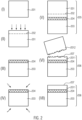
- FIG. 2 A second exemplary embodiment of a process for the manufacture of a high resistivity semiconductor substrate will now be described with reference to Fig. 2 .
- the second embodiment repeats all the characteristics of the first embodiment and in addition gives details of optional process stages.
- a donor substrate 201 which can be the same as the donor substrate 101 of the first embodiment, is first of all provided.
- the substrate 201 can thus also be a semiconductor material, such as silicon, germanium or a compound of silicon and of germanium. More generally, the donor substrate can comprise one or more alloys of semiconductors III-V and/or one or more alloys of semiconductors of Group IV.
- Stage (II) of Fig. 2 illustrates that the donor substrate 201 can subsequently be subjected to a stage of in-depth weakening in order to provide an in-depth weakened layer 202 for the purpose of carrying out a layer transfer towards a receiver substrate, as in the first embodiment.
- This stage can be carried out in particular by ion implantation, especially by implantation of ionic entities, such as H + and/or He + .
- a substrate 203 comprising a layer of oxide 204 at the surface is also provided for the purpose of receiving a transferred semiconductor layer.
- the substrate 203 of the second embodiment can thus comprise silicon and in particular interstitial oxygen with a concentration of at least approximately 12 ⁇ 10 17 atoms ⁇ cm -3 .
- the layer of oxide 204 can once more be a layer of a natural oxide, a layer of SiO 2 , obtained by growth or else deposited, or also an insulator used in semiconductors of alumina (Al 2 O 3 ) type or of nitride type, such as Si 3 N 4 .
- the substrate 203 comprising the layer of oxide 204 at the surface is subjected to at least one stage of stabilization treatment of the interstitial oxygen.
- the stabilization treatment can be a stage of nucleation, precipitation and growth of the precipitates. It can thus be a heat treatment comprising several stationary temperature phases. This treatment, in particular a stationary temperature phase, can be carried out under an atmosphere of oxidizing type, in particular based on water and on oxygen, or else under an atmosphere of nonoxidizing type, in particular of neutral type, with a gas based on argon.
- the substrate 203 comprising the layer of oxide 204 can thus also be subjected to a temperature, in particular to stationary temperature phases, within the range from approximately 650°C to approximately 1200°C. Furthermore, this treatment, in particular each stationary temperature phase, can last from approximately 30 min to approximately 10 h, preferably from approximately 1 h to approximately 8 h.
- the donor substrate 201 and the receiver substrate 203 are adhesively bonded at the level of the layer of oxide 204, so as to form a compound substrate 205 of the SOI type with the layer of buried oxide 204.
- the adhesive bonding can be carried out by molecular adhesion or any other method for the adhesive bonding of semiconductor layers.
- Stage (VI) of Fig. 2 the stage of adhesive bonding is also followed by a stage of cleaving in which a portion 2012 of the donor substrate 201 is detached from the compound substrate 205 by cleaving at the level of the in-depth weakened layer 202, so as to leave a transferred layer 2011 of the donor substrate 201 attached to the receiver substrate 203 by the oxide layer 204, thus forming a new compound substrate 206 comprising the transferred layer 2011.
- a cleaving stage can be carried out by subjecting the compound substrate 205 to a temperature in a range from approximately 300°C to approximately 600°C for a period of time of approximately 30 min to approximately 5 h, under a neutral atmosphere of N 2 or of Ar.
- Stage (VII) of Fig. 2 illustrates an optional subsequent smoothing stage which makes it possible to improve the roughness of the exposed surface 207 of the transferred layer 2011.
- This stage can be carried out by carrying out a heat treatment comprising one or more annealings, preferably one or more rapid annealings, i.e. RTAs.
- the compound substrate 206 can then be exposed to a temperature within a range from approximately 1075°C to approximately 1250°C, preferably from approximately 1175°C to approximately 1230°C, in particular a temperature of approximately 1200°C, this being done for a period of time within the range from approximately 15 s to approximately 120 s, preferably from approximately 20 s to approximately 90 s, in particular a period of time of approximately 30 s, under an atmosphere of the nonoxidizing type, in particular comprising argon and/or hydrogen in a composition which can range from 0% to approximately 50% of hydrogen.
- the residue 2012 of the donor substrate 201 can also be recycled in order to form a new donor substrate in another layer transfer process.
- the second embodiment it is possible in the second embodiment to obtain compound substrates 205 and 206 of HiOi HR SOI type, namely of the type of high resistivity silicon-on-insulator having a high concentration of interstitial oxygen.
- the said at least one stage of stabilization of the interstitial oxygen was carried out before the layer transfer, in other words before the cleaving stage, and thus before any smoothing annealing, just as in the first embodiment, it is possible in the second embodiment to obtain HiOi HR SOI substrates with interface state densities of less than 5 ⁇ 10 11 cm -2 ⁇ eV -1 and mobilities of the carriers in the SOI of greater than 700 cm 2 ⁇ V -1 ⁇ s -1 for the electrons.
- the fixed charge values in the buried oxide can then be less than 3 ⁇ 10 10 cm -2 and the crest interface state densities can be less than 5 ⁇ 10 10 cm -2 ⁇ eV -1 .
- the electrical properties (in particular interfacial properties) of the compound substrates 205 and 206 are also very markedly improved in comparison with HiOi HR SOI substrates obtained by conventional methods, that is to say for which the stabilization stage would have been carried out after the smoothing annealing(s).
Landscapes
- Recrystallisation Techniques (AREA)
- Element Separation (AREA)
Claims (13)
- Verfahren für Herstellung eines hochohmigen Halbleitersubstrats, das die folgenden Schritte umfasst:Bereitstellen eines ersten Substrats (101) mit einer in der Tiefe geschwächten Schicht (102);Bereitstellen eines zweiten Substrats (103) mit einer Schicht aus einem Oxid (104) an der Oberfläche;Verbinden des ersten Substrats (101) mit dem zweiten Substrat (103), um ein Verbund-Substrat (105) auszubilden, das eine vergrabene Oxidschicht (104) umfasst; sowieAufspalten des Verbund-Substrats (105) auf der Ebene der geschwächten Schicht (102); wobeidas Verfahren zusätzlich wenigstens einen Schritt für Stabilisierung, insbesondere eine Stabilisierungs-Wärmebehandlung, des zweiten Substrats (103) mit der Oxidschicht (104) vor dem Schritt zum Aufspalten auf der Ebene der geschwächten Schicht (102) umfasst, undder wenigstens eine Schritt für Stabilisierung ein Schritt für Keimbildung, Präzipitation und Wachstum der Präzipitate ist,dadurch gekennzeichnet, dassder wenigstens eine Schritt für Stabilisierung des zweiten Substrats (103) mit der Oxidschicht (104) vor dem Schritt für Verbindung der zwei Substrate (101, 103) ausgeführt wird.
- Verfahren nach Anspruch 1, wobei der wenigstens eine Schritt für Stabilisierung eine Wärmebehandlung ist, die mehrere Phasen gleichbleibender Temperatur umfasst.
- Verfahren nach einem der Ansprüche 1 und 2, wobei die geschwächte Schicht (102) mittels lonenimplantation in dem ersten Substrat (101) geschaffen wird.
- Verfahren nach einem der vorangehenden Ansprüche, wobei das erste Substrat (101) ein Halbleitermaterial, insbesondere Silizium, Germanium oder eine Verbindung aus Silizium und aus Germanium, und/oder eine oder mehrere Legierung/en von Halbleitern der Gruppen III-V und/oder eine oder mehrere Legierung/en von Halbleitern von Gruppe IV, umfasst.
- Verfahren nach einem der vorangehenden Ansprüche, wobei das zweite Substrat (103) Silizium, insbesondere mit einer hohen Konzentration an eingelagertem Sauerstoff, vorzugsweise Silizium mit einer Konzentration an eingelagertem Sauerstoff von wenigstens etwa 12 * 1017 Atomen·cm-3, umfasst.
- Verfahren nach einem der vorangehenden Ansprüche, wobei der wenigstens eine Schritt für Stabilisierung eine Wärmebehandlung ist, die mit mehrere gleichbleibende Phasen bei Temperaturen innerhalb des Bereiches von ungefähr 650 °C bis ungefähr 1200 °C umfasst.
- Verfahren nach Anspruch 6, wobei die Dauer einer Phase gleichbleibender Temperatur innerhalb des Bereiches, der sich von ungefähr 30 min bis ungefähr 10 h erstreckt, vorzugsweise innerhalb des Bereiches von ungefähr 1 h bis ungefähr 8 h , liegt.
- Verfahren nach einem der Ansprüche 6 und 7, wobei die Atmosphäre einer Phase gleichbleibender Temperatur vom oxidierenden Typ, insbesondere auf Basis von Wasser und Sauerstoff, oder vom nichtoxidierenden Typ, insbesondere vom neutralen Typ, mit einem Gas auf Basis von Argon sein kann.
- Verfahren nach einem der vorangehenden Ansprüche, das zusätzlich wenigstens einen Schritt für Glühen zum Glätten (smoothing annealing), insbesondere einen Schritt für schnelles Glühen (rapid annealing), nach dem Schritt für Aufspaltung des Verbund-Substrats (105) auf der Ebene der geschwächten Schicht (102) umfasst.
- Verfahren nach Anspruch 9, wobei der wenigstens eine Schritt für Glühen zum Glätten bei einer Temperatur im Bereich von ungefähr 1075 °C bis ungefähr 1250 °C, vorzugsweise von ungefähr 1175 °C bis ungefähr 1230 °C, insbesondere bei einer Temperatur von ungefähr 1200 °C, ausgeführt wird.
- Verfahren nach einem der Ansprüche 9 und 10, wobei der wenigstens eine Schritt für Glühen zum Glätten über einen Zeitraum innerhalb des Bereiches von ungefähr 15 s bis ungefähr 120 s, vorzugsweise von ungefähr 20 s bis ungefähr 90 s, insbesondere über einen Zeitraum von ungefähr 30 s, ausgeführt wird.
- Verfahren nach einem der Ansprüche 9 bis 11, wobei der wenigstens eine Schritt für Glühen zum Glätten in einer Atmosphäre vom nichtoxidierenden Typ durchgeführt wird, die insbesondere Argon und/oder Wasserstoff in einer Zusammensetzung von 0 % bis ungefähr 50 % Wasserstoff umfasst.
- Verfahren nach einem der vorangehenden Ansprüche, das zusätzlich einen Schritt für Wiederverwendung eines Rückstandes (1012) des ersten Substrats (101) nach dem Schritt für Aufspaltung des Verbund-Substrats (105) auf der Ebene der geschwächten Schicht (102) umfasst.
Applications Claiming Priority (1)
| Application Number | Priority Date | Filing Date | Title |
|---|---|---|---|
| FR1654689A FR3051968B1 (fr) | 2016-05-25 | 2016-05-25 | Procede de fabrication d'un substrat semi-conducteur a haute resistivite |
Publications (2)
| Publication Number | Publication Date |
|---|---|
| EP3249683A1 EP3249683A1 (de) | 2017-11-29 |
| EP3249683B1 true EP3249683B1 (de) | 2023-03-01 |
Family
ID=56404192
Family Applications (1)
| Application Number | Title | Priority Date | Filing Date |
|---|---|---|---|
| EP17171861.2A Active EP3249683B1 (de) | 2016-05-25 | 2017-05-19 | Verfahren zur herstellung eines halbleitersubstrats mit hohem widerstand |
Country Status (8)
| Country | Link |
|---|---|
| US (1) | US10163682B2 (de) |
| EP (1) | EP3249683B1 (de) |
| JP (1) | JP6482595B2 (de) |
| KR (1) | KR101991091B1 (de) |
| CN (1) | CN107437526A (de) |
| FR (1) | FR3051968B1 (de) |
| SG (1) | SG10201704204RA (de) |
| TW (1) | TWI629725B (de) |
Families Citing this family (7)
| Publication number | Priority date | Publication date | Assignee | Title |
|---|---|---|---|---|
| FR3074608B1 (fr) * | 2017-12-05 | 2019-12-06 | Soitec | Procede de preparation d'un residu de substrat donneur, substrat obtenu a l'issu de ce procede, et utilisation d'un tel susbtrat |
| FR3091010B1 (fr) * | 2018-12-24 | 2020-12-04 | Soitec Silicon On Insulator | Structure de type semi-conducteur pour applications digitales et radiofréquences, et procédé de fabrication d’une telle structure |
| FR3106019B1 (fr) * | 2020-01-07 | 2021-12-10 | Soitec Silicon On Insulator | Procede de fabrication d’une structure de type semi-conducteur sur isolant pour applications radiofréquences |
| FR3108204B1 (fr) * | 2020-03-10 | 2023-10-27 | Commissariat Energie Atomique | Procédé de suspension d’une couche mince sur une cavité avec effet raidisseur obtenu par pressurisation de la cavité par des espèces implantées |
| FR3119929B1 (fr) * | 2021-02-15 | 2023-11-03 | Soitec Silicon On Insulator | Procede de fabrication d’une structure adaptee pour les applications radiofrequences, et substrat support pour ladite structure |
| US11955374B2 (en) * | 2021-08-29 | 2024-04-09 | Taiwan Semiconductor Manufacturing Company, Ltd. | Method for forming SOI substrate |
| CN114156179A (zh) * | 2021-10-29 | 2022-03-08 | 中国科学院上海微系统与信息技术研究所 | 一种改善绝缘层上硅晶圆表面粗糙度的方法 |
Citations (1)
| Publication number | Priority date | Publication date | Assignee | Title |
|---|---|---|---|---|
| US20150132923A1 (en) * | 2011-11-30 | 2015-05-14 | Soitec | Process for fabricating a heterostructure limiting the formation of defects |
Family Cites Families (16)
| Publication number | Priority date | Publication date | Assignee | Title |
|---|---|---|---|---|
| EP1087041B1 (de) * | 1999-03-16 | 2009-01-07 | Shin-Etsu Handotai Co., Ltd | Herstellungsverfahren für siliziumwafer und siliziumwafer |
| JP2004537161A (ja) * | 2001-04-11 | 2004-12-09 | エムイーエムシー・エレクトロニック・マテリアルズ・インコーポレイテッド | 高抵抗率czシリコンにおけるサーマルドナー生成の制御 |
| FR2838865B1 (fr) | 2002-04-23 | 2005-10-14 | Soitec Silicon On Insulator | Procede de fabrication d'un substrat avec couche utile sur support de resistivite elevee |
| JP2004006615A (ja) * | 2002-04-26 | 2004-01-08 | Sumitomo Mitsubishi Silicon Corp | 高抵抗シリコンウエーハ及びその製造方法 |
| WO2004008521A1 (ja) * | 2002-07-17 | 2004-01-22 | Sumitomo Mitsubishi Silicon Corporation | 高抵抗シリコンウエーハ及びその製造方法 |
| FR2858462B1 (fr) | 2003-07-29 | 2005-12-09 | Soitec Silicon On Insulator | Procede d'obtention d'une couche mince de qualite accrue par co-implantation et recuit thermique |
| JP2005064405A (ja) | 2003-08-20 | 2005-03-10 | Shin Etsu Handotai Co Ltd | シリコンウェーハの製造方法及びシリコンウェーハ |
| CN100461349C (zh) * | 2003-10-21 | 2009-02-11 | 株式会社上睦可 | 高电阻硅晶片的制造方法以及外延晶片及soi晶片的制造方法 |
| JP4655557B2 (ja) | 2004-09-10 | 2011-03-23 | 信越半導体株式会社 | Soi基板の製造方法及びsoi基板 |
| EP1835533B1 (de) | 2006-03-14 | 2020-06-03 | Soitec | Verfahren zum Herstellen von zusammengesetzten Hableiterscheiben und Verfahren zur Wiederverwendung des gebrauchten Substrats |
| FR2943458B1 (fr) | 2009-03-18 | 2011-06-10 | Soitec Silicon On Insulator | Procede de finition d'un substrat de type "silicium sur isolant" soi |
| FR2953640B1 (fr) * | 2009-12-04 | 2012-02-10 | S O I Tec Silicon On Insulator Tech | Procede de fabrication d'une structure de type semi-conducteur sur isolant, a pertes electriques diminuees et structure correspondante |
| CN102130037B (zh) * | 2010-12-27 | 2013-03-13 | 上海新傲科技股份有限公司 | 采用吸杂工艺制备带有绝缘埋层的半导体衬底的方法 |
| JP6036732B2 (ja) | 2014-03-18 | 2016-11-30 | 信越半導体株式会社 | 貼り合わせウェーハの製造方法 |
| CN104952726A (zh) * | 2014-03-26 | 2015-09-30 | 中芯国际集成电路制造(上海)有限公司 | 一种用于无源器件的半导体衬底的制作方法 |
| JP2016082093A (ja) * | 2014-10-17 | 2016-05-16 | 信越半導体株式会社 | 貼り合わせウェーハの製造方法 |
-
2016
- 2016-05-25 FR FR1654689A patent/FR3051968B1/fr active Active
-
2017
- 2017-05-12 TW TW106115750A patent/TWI629725B/zh active
- 2017-05-18 JP JP2017099123A patent/JP6482595B2/ja active Active
- 2017-05-19 EP EP17171861.2A patent/EP3249683B1/de active Active
- 2017-05-23 KR KR1020170063549A patent/KR101991091B1/ko active Active
- 2017-05-23 SG SG10201704204RA patent/SG10201704204RA/en unknown
- 2017-05-24 US US15/603,830 patent/US10163682B2/en active Active
- 2017-05-24 CN CN201710375239.0A patent/CN107437526A/zh active Pending
Patent Citations (1)
| Publication number | Priority date | Publication date | Assignee | Title |
|---|---|---|---|---|
| US20150132923A1 (en) * | 2011-11-30 | 2015-05-14 | Soitec | Process for fabricating a heterostructure limiting the formation of defects |
Also Published As
| Publication number | Publication date |
|---|---|
| EP3249683A1 (de) | 2017-11-29 |
| JP2018011042A (ja) | 2018-01-18 |
| US20170345709A1 (en) | 2017-11-30 |
| FR3051968B1 (fr) | 2018-06-01 |
| JP6482595B2 (ja) | 2019-03-13 |
| FR3051968A1 (fr) | 2017-12-01 |
| SG10201704204RA (en) | 2017-12-28 |
| KR101991091B1 (ko) | 2019-06-20 |
| CN107437526A (zh) | 2017-12-05 |
| TW201742152A (zh) | 2017-12-01 |
| KR20170133273A (ko) | 2017-12-05 |
| TWI629725B (zh) | 2018-07-11 |
| US10163682B2 (en) | 2018-12-25 |
Similar Documents
| Publication | Publication Date | Title |
|---|---|---|
| EP3249683B1 (de) | Verfahren zur herstellung eines halbleitersubstrats mit hohem widerstand | |
| US7268060B2 (en) | Method for fabricating a substrate with useful layer on high resistivity support | |
| JP6637515B2 (ja) | 半導体オン・インシュレータ構造の製造において使用するための熱的に安定した電荷トラップ層 | |
| EP3792965B1 (de) | Silizium-auf-isolator-substrat mit hohem widerstand und verbesserter ladungsabfangender effizienz | |
| KR102285114B1 (ko) | 접합 soi 웨이퍼의 제조방법 및 접합 soi 웨이퍼 | |
| US7645684B2 (en) | Wafer and method of producing a substrate by transfer of a layer that includes foreign species | |
| TWI335614B (en) | Method of producing bonded wafer | |
| US7572714B2 (en) | Film taking-off method | |
| KR102327330B1 (ko) | Soi웨이퍼의 제조방법 | |
| CN114730699A (zh) | 制造包括位于由SiC制成的载体基板上的单晶SiC薄层的复合结构的方法 | |
| JPWO2005024917A1 (ja) | 貼り合わせウェーハの製造方法 | |
| US7285471B2 (en) | Process for transfer of a thin layer formed in a substrate with vacancy clusters | |
| JP4926077B2 (ja) | 溶融層を用いた歪み層の歪み緩和 | |
| US6939783B2 (en) | Preventive treatment method for a multilayer semiconductor wafer | |
| JP5125194B2 (ja) | 貼り合わせウエーハの製造方法 | |
| US20050202658A1 (en) | Method for limiting slip lines in a semiconductor substrate |
Legal Events
| Date | Code | Title | Description |
|---|---|---|---|
| PUAI | Public reference made under article 153(3) epc to a published international application that has entered the european phase |
Free format text: ORIGINAL CODE: 0009012 |
|
| STAA | Information on the status of an ep patent application or granted ep patent |
Free format text: STATUS: THE APPLICATION HAS BEEN PUBLISHED |
|
| AK | Designated contracting states |
Kind code of ref document: A1 Designated state(s): AL AT BE BG CH CY CZ DE DK EE ES FI FR GB GR HR HU IE IS IT LI LT LU LV MC MK MT NL NO PL PT RO RS SE SI SK SM TR |
|
| AX | Request for extension of the european patent |
Extension state: BA ME |
|
| STAA | Information on the status of an ep patent application or granted ep patent |
Free format text: STATUS: REQUEST FOR EXAMINATION WAS MADE |
|
| 17P | Request for examination filed |
Effective date: 20180108 |
|
| RBV | Designated contracting states (corrected) |
Designated state(s): AL AT BE BG CH CY CZ DE DK EE ES FI FR GB GR HR HU IE IS IT LI LT LU LV MC MK MT NL NO PL PT RO RS SE SI SK SM TR |
|
| STAA | Information on the status of an ep patent application or granted ep patent |
Free format text: STATUS: EXAMINATION IS IN PROGRESS |
|
| 17Q | First examination report despatched |
Effective date: 20210216 |
|
| GRAP | Despatch of communication of intention to grant a patent |
Free format text: ORIGINAL CODE: EPIDOSNIGR1 |
|
| STAA | Information on the status of an ep patent application or granted ep patent |
Free format text: STATUS: GRANT OF PATENT IS INTENDED |
|
| INTG | Intention to grant announced |
Effective date: 20220908 |
|
| GRAS | Grant fee paid |
Free format text: ORIGINAL CODE: EPIDOSNIGR3 |
|
| GRAA | (expected) grant |
Free format text: ORIGINAL CODE: 0009210 |
|
| STAA | Information on the status of an ep patent application or granted ep patent |
Free format text: STATUS: THE PATENT HAS BEEN GRANTED |
|
| AK | Designated contracting states |
Kind code of ref document: B1 Designated state(s): AL AT BE BG CH CY CZ DE DK EE ES FI FR GB GR HR HU IE IS IT LI LT LU LV MC MK MT NL NO PL PT RO RS SE SI SK SM TR |
|
| REG | Reference to a national code |
Ref country code: GB Ref legal event code: FG4D |
|
| REG | Reference to a national code |
Ref country code: CH Ref legal event code: EP Ref country code: AT Ref legal event code: REF Ref document number: 1551586 Country of ref document: AT Kind code of ref document: T Effective date: 20230315 |
|
| REG | Reference to a national code |
Ref country code: DE Ref legal event code: R096 Ref document number: 602017066352 Country of ref document: DE |
|
| REG | Reference to a national code |
Ref country code: IE Ref legal event code: FG4D |
|
| REG | Reference to a national code |
Ref country code: FR Ref legal event code: PLFP Year of fee payment: 7 |
|
| REG | Reference to a national code |
Ref country code: LT Ref legal event code: MG9D |
|
| REG | Reference to a national code |
Ref country code: NL Ref legal event code: MP Effective date: 20230301 |
|
| PG25 | Lapsed in a contracting state [announced via postgrant information from national office to epo] |
Ref country code: RS Free format text: LAPSE BECAUSE OF FAILURE TO SUBMIT A TRANSLATION OF THE DESCRIPTION OR TO PAY THE FEE WITHIN THE PRESCRIBED TIME-LIMIT Effective date: 20230301 Ref country code: NO Free format text: LAPSE BECAUSE OF FAILURE TO SUBMIT A TRANSLATION OF THE DESCRIPTION OR TO PAY THE FEE WITHIN THE PRESCRIBED TIME-LIMIT Effective date: 20230601 Ref country code: LV Free format text: LAPSE BECAUSE OF FAILURE TO SUBMIT A TRANSLATION OF THE DESCRIPTION OR TO PAY THE FEE WITHIN THE PRESCRIBED TIME-LIMIT Effective date: 20230301 Ref country code: LT Free format text: LAPSE BECAUSE OF FAILURE TO SUBMIT A TRANSLATION OF THE DESCRIPTION OR TO PAY THE FEE WITHIN THE PRESCRIBED TIME-LIMIT Effective date: 20230301 Ref country code: HR Free format text: LAPSE BECAUSE OF FAILURE TO SUBMIT A TRANSLATION OF THE DESCRIPTION OR TO PAY THE FEE WITHIN THE PRESCRIBED TIME-LIMIT Effective date: 20230301 Ref country code: ES Free format text: LAPSE BECAUSE OF FAILURE TO SUBMIT A TRANSLATION OF THE DESCRIPTION OR TO PAY THE FEE WITHIN THE PRESCRIBED TIME-LIMIT Effective date: 20230301 |
|
| PG25 | Lapsed in a contracting state [announced via postgrant information from national office to epo] |
Ref country code: SE Free format text: LAPSE BECAUSE OF FAILURE TO SUBMIT A TRANSLATION OF THE DESCRIPTION OR TO PAY THE FEE WITHIN THE PRESCRIBED TIME-LIMIT Effective date: 20230301 Ref country code: PL Free format text: LAPSE BECAUSE OF FAILURE TO SUBMIT A TRANSLATION OF THE DESCRIPTION OR TO PAY THE FEE WITHIN THE PRESCRIBED TIME-LIMIT Effective date: 20230301 Ref country code: NL Free format text: LAPSE BECAUSE OF FAILURE TO SUBMIT A TRANSLATION OF THE DESCRIPTION OR TO PAY THE FEE WITHIN THE PRESCRIBED TIME-LIMIT Effective date: 20230301 Ref country code: GR Free format text: LAPSE BECAUSE OF FAILURE TO SUBMIT A TRANSLATION OF THE DESCRIPTION OR TO PAY THE FEE WITHIN THE PRESCRIBED TIME-LIMIT Effective date: 20230602 Ref country code: FI Free format text: LAPSE BECAUSE OF FAILURE TO SUBMIT A TRANSLATION OF THE DESCRIPTION OR TO PAY THE FEE WITHIN THE PRESCRIBED TIME-LIMIT Effective date: 20230301 |
|
| PG25 | Lapsed in a contracting state [announced via postgrant information from national office to epo] |
Ref country code: SM Free format text: LAPSE BECAUSE OF FAILURE TO SUBMIT A TRANSLATION OF THE DESCRIPTION OR TO PAY THE FEE WITHIN THE PRESCRIBED TIME-LIMIT Effective date: 20230301 Ref country code: RO Free format text: LAPSE BECAUSE OF FAILURE TO SUBMIT A TRANSLATION OF THE DESCRIPTION OR TO PAY THE FEE WITHIN THE PRESCRIBED TIME-LIMIT Effective date: 20230301 Ref country code: PT Free format text: LAPSE BECAUSE OF FAILURE TO SUBMIT A TRANSLATION OF THE DESCRIPTION OR TO PAY THE FEE WITHIN THE PRESCRIBED TIME-LIMIT Effective date: 20230703 Ref country code: EE Free format text: LAPSE BECAUSE OF FAILURE TO SUBMIT A TRANSLATION OF THE DESCRIPTION OR TO PAY THE FEE WITHIN THE PRESCRIBED TIME-LIMIT Effective date: 20230301 Ref country code: CZ Free format text: LAPSE BECAUSE OF FAILURE TO SUBMIT A TRANSLATION OF THE DESCRIPTION OR TO PAY THE FEE WITHIN THE PRESCRIBED TIME-LIMIT Effective date: 20230301 |
|
| PG25 | Lapsed in a contracting state [announced via postgrant information from national office to epo] |
Ref country code: SK Free format text: LAPSE BECAUSE OF FAILURE TO SUBMIT A TRANSLATION OF THE DESCRIPTION OR TO PAY THE FEE WITHIN THE PRESCRIBED TIME-LIMIT Effective date: 20230301 Ref country code: IS Free format text: LAPSE BECAUSE OF FAILURE TO SUBMIT A TRANSLATION OF THE DESCRIPTION OR TO PAY THE FEE WITHIN THE PRESCRIBED TIME-LIMIT Effective date: 20230701 |
|
| REG | Reference to a national code |
Ref country code: DE Ref legal event code: R097 Ref document number: 602017066352 Country of ref document: DE |
|
| REG | Reference to a national code |
Ref country code: CH Ref legal event code: PL |
|
| PLBE | No opposition filed within time limit |
Free format text: ORIGINAL CODE: 0009261 |
|
| STAA | Information on the status of an ep patent application or granted ep patent |
Free format text: STATUS: NO OPPOSITION FILED WITHIN TIME LIMIT |
|
| REG | Reference to a national code |
Ref country code: AT Ref legal event code: UEP Ref document number: 1551586 Country of ref document: AT Kind code of ref document: T Effective date: 20230301 |
|
| PG25 | Lapsed in a contracting state [announced via postgrant information from national office to epo] |
Ref country code: MC Free format text: LAPSE BECAUSE OF FAILURE TO SUBMIT A TRANSLATION OF THE DESCRIPTION OR TO PAY THE FEE WITHIN THE PRESCRIBED TIME-LIMIT Effective date: 20230301 |
|
| REG | Reference to a national code |
Ref country code: BE Ref legal event code: MM Effective date: 20230531 |
|
| PG25 | Lapsed in a contracting state [announced via postgrant information from national office to epo] |
Ref country code: SI Free format text: LAPSE BECAUSE OF FAILURE TO SUBMIT A TRANSLATION OF THE DESCRIPTION OR TO PAY THE FEE WITHIN THE PRESCRIBED TIME-LIMIT Effective date: 20230301 Ref country code: MC Free format text: LAPSE BECAUSE OF FAILURE TO SUBMIT A TRANSLATION OF THE DESCRIPTION OR TO PAY THE FEE WITHIN THE PRESCRIBED TIME-LIMIT Effective date: 20230301 Ref country code: LU Free format text: LAPSE BECAUSE OF NON-PAYMENT OF DUE FEES Effective date: 20230519 Ref country code: LI Free format text: LAPSE BECAUSE OF NON-PAYMENT OF DUE FEES Effective date: 20230531 Ref country code: DK Free format text: LAPSE BECAUSE OF FAILURE TO SUBMIT A TRANSLATION OF THE DESCRIPTION OR TO PAY THE FEE WITHIN THE PRESCRIBED TIME-LIMIT Effective date: 20230301 Ref country code: CH Free format text: LAPSE BECAUSE OF NON-PAYMENT OF DUE FEES Effective date: 20230531 |
|
| 26N | No opposition filed |
Effective date: 20231204 |
|
| GBPC | Gb: european patent ceased through non-payment of renewal fee |
Effective date: 20230601 |
|
| REG | Reference to a national code |
Ref country code: IE Ref legal event code: MM4A |
|
| PG25 | Lapsed in a contracting state [announced via postgrant information from national office to epo] |
Ref country code: IE Free format text: LAPSE BECAUSE OF NON-PAYMENT OF DUE FEES Effective date: 20230519 |
|
| PG25 | Lapsed in a contracting state [announced via postgrant information from national office to epo] |
Ref country code: IE Free format text: LAPSE BECAUSE OF NON-PAYMENT OF DUE FEES Effective date: 20230519 Ref country code: GB Free format text: LAPSE BECAUSE OF NON-PAYMENT OF DUE FEES Effective date: 20230601 |
|
| PG25 | Lapsed in a contracting state [announced via postgrant information from national office to epo] |
Ref country code: BE Free format text: LAPSE BECAUSE OF NON-PAYMENT OF DUE FEES Effective date: 20230531 |
|
| PG25 | Lapsed in a contracting state [announced via postgrant information from national office to epo] |
Ref country code: BG Free format text: LAPSE BECAUSE OF FAILURE TO SUBMIT A TRANSLATION OF THE DESCRIPTION OR TO PAY THE FEE WITHIN THE PRESCRIBED TIME-LIMIT Effective date: 20230301 |
|
| PG25 | Lapsed in a contracting state [announced via postgrant information from national office to epo] |
Ref country code: BG Free format text: LAPSE BECAUSE OF FAILURE TO SUBMIT A TRANSLATION OF THE DESCRIPTION OR TO PAY THE FEE WITHIN THE PRESCRIBED TIME-LIMIT Effective date: 20230301 |
|
| PGFP | Annual fee paid to national office [announced via postgrant information from national office to epo] |
Ref country code: DE Payment date: 20250402 Year of fee payment: 9 |
|
| PGFP | Annual fee paid to national office [announced via postgrant information from national office to epo] |
Ref country code: IT Payment date: 20250422 Year of fee payment: 9 |
|
| PGFP | Annual fee paid to national office [announced via postgrant information from national office to epo] |
Ref country code: FR Payment date: 20250401 Year of fee payment: 9 |
|
| PGFP | Annual fee paid to national office [announced via postgrant information from national office to epo] |
Ref country code: AT Payment date: 20250425 Year of fee payment: 9 |
|
| PG25 | Lapsed in a contracting state [announced via postgrant information from national office to epo] |
Ref country code: CY Free format text: LAPSE BECAUSE OF FAILURE TO SUBMIT A TRANSLATION OF THE DESCRIPTION OR TO PAY THE FEE WITHIN THE PRESCRIBED TIME-LIMIT; INVALID AB INITIO Effective date: 20170519 |
|
| PG25 | Lapsed in a contracting state [announced via postgrant information from national office to epo] |
Ref country code: HU Free format text: LAPSE BECAUSE OF FAILURE TO SUBMIT A TRANSLATION OF THE DESCRIPTION OR TO PAY THE FEE WITHIN THE PRESCRIBED TIME-LIMIT; INVALID AB INITIO Effective date: 20170519 |
|
| REG | Reference to a national code |
Ref country code: DE Ref legal event code: R079 Ref document number: 602017066352 Country of ref document: DE Free format text: PREVIOUS MAIN CLASS: H01L0021762000 Ipc: H10W0010100000 |
|
| PG25 | Lapsed in a contracting state [announced via postgrant information from national office to epo] |
Ref country code: TR Free format text: LAPSE BECAUSE OF FAILURE TO SUBMIT A TRANSLATION OF THE DESCRIPTION OR TO PAY THE FEE WITHIN THE PRESCRIBED TIME-LIMIT Effective date: 20230301 |