EP3272026B1 - Module pour combinant des signaux ayant différentes fréquences - Google Patents
Module pour combinant des signaux ayant différentes fréquences Download PDFInfo
- Publication number
- EP3272026B1 EP3272026B1 EP15794973.6A EP15794973A EP3272026B1 EP 3272026 B1 EP3272026 B1 EP 3272026B1 EP 15794973 A EP15794973 A EP 15794973A EP 3272026 B1 EP3272026 B1 EP 3272026B1
- Authority
- EP
- European Patent Office
- Prior art keywords
- signals
- frequency
- frequency combiner
- combiner
- telecommunications system
- Prior art date
- Legal status (The legal status is an assumption and is not a legal conclusion. Google has not performed a legal analysis and makes no representation as to the accuracy of the status listed.)
- Active
Links
Images


Classifications
-
- H—ELECTRICITY
- H04—ELECTRIC COMMUNICATION TECHNIQUE
- H04L—TRANSMISSION OF DIGITAL INFORMATION, e.g. TELEGRAPHIC COMMUNICATION
- H04L27/00—Modulated-carrier systems
- H04L27/26—Systems using multi-frequency codes
- H04L27/28—Systems using multi-frequency codes with simultaneous transmission of different frequencies each representing one code element
-
- H—ELECTRICITY
- H04—ELECTRIC COMMUNICATION TECHNIQUE
- H04B—TRANSMISSION
- H04B1/00—Details of transmission systems, not covered by a single one of groups H04B3/00 - H04B13/00; Details of transmission systems not characterised by the medium used for transmission
- H04B1/005—Details of transmission systems, not covered by a single one of groups H04B3/00 - H04B13/00; Details of transmission systems not characterised by the medium used for transmission adapting radio receivers, transmitters andtransceivers for operation on two or more bands, i.e. frequency ranges
- H04B1/0053—Details of transmission systems, not covered by a single one of groups H04B3/00 - H04B13/00; Details of transmission systems not characterised by the medium used for transmission adapting radio receivers, transmitters andtransceivers for operation on two or more bands, i.e. frequency ranges with common antenna for more than one band
- H04B1/0057—Details of transmission systems, not covered by a single one of groups H04B3/00 - H04B13/00; Details of transmission systems not characterised by the medium used for transmission adapting radio receivers, transmitters andtransceivers for operation on two or more bands, i.e. frequency ranges with common antenna for more than one band using diplexing or multiplexing filters for selecting the desired band
-
- H—ELECTRICITY
- H04—ELECTRIC COMMUNICATION TECHNIQUE
- H04B—TRANSMISSION
- H04B1/00—Details of transmission systems, not covered by a single one of groups H04B3/00 - H04B13/00; Details of transmission systems not characterised by the medium used for transmission
- H04B1/38—Transceivers, i.e. devices in which transmitter and receiver form a structural unit and in which at least one part is used for functions of transmitting and receiving
- H04B1/40—Circuits
- H04B1/401—Circuits for selecting or indicating operating mode
-
- H—ELECTRICITY
- H04—ELECTRIC COMMUNICATION TECHNIQUE
- H04B—TRANSMISSION
- H04B7/00—Radio transmission systems, i.e. using radiation field
- H04B7/02—Diversity systems; Multi-antenna system, i.e. transmission or reception using multiple antennas
-
- H—ELECTRICITY
- H04—ELECTRIC COMMUNICATION TECHNIQUE
- H04B—TRANSMISSION
- H04B7/00—Radio transmission systems, i.e. using radiation field
- H04B7/02—Diversity systems; Multi-antenna system, i.e. transmission or reception using multiple antennas
- H04B7/12—Frequency diversity
-
- H—ELECTRICITY
- H04—ELECTRIC COMMUNICATION TECHNIQUE
- H04B—TRANSMISSION
- H04B7/00—Radio transmission systems, i.e. using radiation field
- H04B7/14—Relay systems
- H04B7/15—Active relay systems
- H04B7/155—Ground-based stations
-
- H—ELECTRICITY
- H04—ELECTRIC COMMUNICATION TECHNIQUE
- H04L—TRANSMISSION OF DIGITAL INFORMATION, e.g. TELEGRAPHIC COMMUNICATION
- H04L1/00—Arrangements for detecting or preventing errors in the information received
- H04L1/02—Arrangements for detecting or preventing errors in the information received by diversity reception
- H04L1/04—Arrangements for detecting or preventing errors in the information received by diversity reception using frequency diversity
-
- G—PHYSICS
- G10—MUSICAL INSTRUMENTS; ACOUSTICS
- G10L—SPEECH ANALYSIS TECHNIQUES OR SPEECH SYNTHESIS; SPEECH RECOGNITION; SPEECH OR VOICE PROCESSING TECHNIQUES; SPEECH OR AUDIO CODING OR DECODING
- G10L19/00—Speech or audio signals analysis-synthesis techniques for redundancy reduction, e.g. in vocoders; Coding or decoding of speech or audio signals, using source filter models or psychoacoustic analysis
- G10L19/04—Speech or audio signals analysis-synthesis techniques for redundancy reduction, e.g. in vocoders; Coding or decoding of speech or audio signals, using source filter models or psychoacoustic analysis using predictive techniques
- G10L19/08—Determination or coding of the excitation function; Determination or coding of the long-term prediction parameters
- G10L19/093—Determination or coding of the excitation function; Determination or coding of the long-term prediction parameters using sinusoidal excitation models
Definitions
- the disclosure relates generally to telecommunications and, more particularly (although not necessarily exclusively), to a frequency combiner for adjusting signal-processing parameters and combining signals of multiple frequency bands.
- multiple frequency bands can be wirelessly received via one or more antennas.
- a DAS or a repeater installation can be used to extend wireless coverage in an area.
- a repeater can receive multiple frequency bands from a base station wirelessly from one or more donor antennas. After amplification to a desired output power, individual transmit and receive paths can be combined using a frequency combiner. The combined signal can be output via one or more RF ports to serve a coverage area.
- a frequency dependent frequency combiner can involve insertion loss and lack flexibility when a frequency band unsupported by the frequency combiner is used.
- one or more head-end units can receive downlink signals on multiple frequency bands from one or more base stations.
- the head-end unit can distribute the downlink signals in analog or digital format to one or more remote units.
- the individual transmit paths can be combined in a multiplexer in a remote unit and output from one or more RF ports to serve a coverage area.
- a frequency dependent multiplexer can lack flexibility when a frequency band unsupported by the multiplexer is used.
- JP 2006 293215 A (Furukawa Electric Co Ltd) published 26 October 2006 discloses a pulse generating unit composed of a pulse supplying unit and a pulse shaping unit.
- the pulse shaping unit is a CPF comprising, for example, four stages each constituted by connecting an HNLF, a dispersion slope compensating fiber (DSCF), and an SMF in this order.
- the pulse shaping unit is so designed that while the HNFL and SMF has positive dispersion slope values, the positive dispersion slope values are compensated with the negative dispersion slope value that the DSCF has to make the respective stages have a cumulative dispersion slope value of 0.
- US 5 838 675 A discloses a channelized protection circuit for protecting the front-end of a receiver from the detrimental effects of interference signals within the bandwidth of received signals.
- the channelized protection circuit comprises: a frequency demultiplexer for separating a broadband input signal into a plurality of different signal components in respective contiguous frequency channels; a plurality of signal conditioning subcircuits respectively responsive to the plurality of different signal components for selectively performing a conditioning operation on the plurality of different signal components to produce a plurality of conditioned signal components minimally affected by interference signals from within any of the contiguous frequency channels; and a frequency multiplexer having a plurality of contiguous frequency channels for recombining the plurality of conditioned signal components into a composite conditioned signal of original bandwidth and at a safe power level with a minimum amount of interference.
- the channelized protection circuit may also include a first plurality of phase-adjusting circuits for compensating for phase imbalances among the plurality of different signal components, and also includes a second plurality of phase-adjusting circuits for compensating for phase imbalances among the plurality of conditioned signal components.
- the optical communications equipment includes a piezoelectric actuator, a moving body moved by the piezoelectric actuator as a drive source, a multi-coating filter for controlling light that is a signal medium by movement of the moving body, a drive circuit for controlling the position of the multi-coating filter via the actuator, and a control circuit.
- the piezoelectric actuator uses bending vibrations produced in a piezoelectric vibrating body as a power source.
- a single weight antenna system for HSDPA may comprise receiving HSDPA signals via a plurality of receive antennas and individually adjusting a phase of a portion of the received HSDPA signals via a single weight.
- the phase adjusted portion of the received HSDPA signals may be combined with at least one of the received HSDPA signals to generate combined HSDPA signals.
- At least one control signal may control the adjusting of the phase of the received HSDPA signals.
- Discrete phases may be communicated to adjust the phase of the portion of the received HSDPA signals, where the plurality of the discrete phases may range from zero radians to substantially 2 ⁇ radians.
- Phase shift channel estimates may be generated during the identified time to determine the discrete phase.
- a desired phase may be generated from the phase shift channel estimates, and the single weight may be generated from the desired phase.
- a frequency combiner can include input ports that receive multiple signals at different frequencies.
- the frequency combiner can include adjustable tuning elements for adjusting the phase shifts of the multiple RF paths using phase shifters.
- the frequency combiner can be frequency independent (e.g., configured to receive and combine signals at any frequency) so that multiple RF modules that each support different frequency bands can be used and adjusted. By adjusting the phase shift of the RF path for each RF module, the frequency combiner can ensure that the RF modules are matched at the output ports.
- the adjustable tuning elements of the frequency combiner can include an electric length tuner for changing a relative permittivity of the transmission line or a tuning line for varying the physical length of the transmission line.
- the frequency combiner can be field-configurable and adjustable while implemented in the telecommunications system.
- a distributed antenna system can include multiple input ports that are each frequency specific.
- the telecommunications system can also include one or more output ports.
- the telecommunications system can include a frequency combiner for combining the multiple input signals for output through the one or more output ports. Adjusting signaling parameters of the frequency combiner can ensure that the phase shifts and other parameters of the multiple RF paths are matched together in the telecommunications system.
- the adjustable elements of the frequency combiner can be tuned manually or automatically so that RF modules with different input frequencies can be swapped in the telecommunications system while in the field. Further, adjustable tuning elements can provide for low passive intermodulation (PIM) to avoid desensitizing the receive path by PIM products created in the transmit path.
- PIM passive intermodulation
- a frequency combiner with adjustable tuning elements can allow for combining input signals of varying frequencies in a telecommunications system while reducing the total number of required frequency-dependent multiplexers. Further, use of a frequency combiner with adjustable elements can offer the flexibility to upgrade and exchange frequency bands in field installations.
- FIG. 1 is a block diagram of an example of a frequency combiner 100 for use in a telecommunications system, such as a DAS or a repeater.
- the frequency combiner 100 can be positioned between multiple input ports and at least one output port of the telecommunications system.
- the frequency combiner can include one or more RF modules 102a-d communicatively coupled to a combiner component 108.
- the combiner component 108 can include circuitry for adjusting signal-processing parameters of the RF paths for combining the signals of the RF modules 102a-d.
- the combiner component 108 can combine signals of varying frequencies.
- the frequency combiner 100 can be frequency independent while the RF modules 102a-d can be frequency dependent (e.g., each tuned to a specific frequency band).
- the RF modules 102a-d can each include input ports 104a-d.
- the input ports 104a-d can respectively include receive (RX) ports 114a-d for receiving RF signals and transmit (TX) ports 116a-d for transmitting RF signals.
- RX receive
- TX transmit
- Each of the RX ports 114a-d and the TX ports 116a-d can be tuned to a different frequency band.
- RF modules 102a-d can be exchanged while the frequency combiner 100 is deployed in a telecommunications system to support different frequencies.
- RF module 102a can include RX port 114a designed to receive signals at frequencies between 925 MHz - 960 MHz and TX port 116a designed to transmit signals between 880 MHz - 915 MHz.
- RF module 102b can include RX port 114b designed to receive signals at frequencies between 791 MHz - 821 MHz and TX port 116b designed to transmit signals between 832 MHz - 862 MHz.
- RF module 102c can include RX port 114c designed to receive signals at frequencies between 1805 MHz - 1880 MHz and TX port 116c designed to transmit signals between 1710 MHz - 1785 MHz.
- RF module 102d can include RX port 114d designed to receive signals at frequencies between 2620 MHz - 2690 MHz and TX port 116d designed to transmit signals at frequencies between 2500 MHz - 2570 MHz.
- a new frequency range can be used within the frequency combiner 100 by swapping an RF module 102 with a new module that supports an RX port for receiving signals at frequencies between 2110 MHz - 2170 MHz and a TX port for transmitting signals at frequencies between 1920 MHz - 1980 MHz.
- Each RF module 102a-d can include amplifiers 106a-h for increasing the gain of signals received on RX ports 114a-d and transmitted on TX ports 116a-d.
- the RF modules 102a-d can be communicatively coupled to a combiner component 108 via duplexers 118a-d.
- Duplexers 118a-d can be used to provide bidirectional communication with the combiner component 108.
- the duplexer 118a allows signals received on RX port 114a and signals transmitted on TX port 116a to share the communications path with the combiner component 108.
- the combiner component 108 can include adjustable tuning elements 110a-d.
- Test signals from each of the RF modules 102a-d can be provided to the combiner component 108 so that by adjusting of certain signal-processing parameters at the respective adjustable tuning elements 110a-d the RF paths can be optimized for combining signals.
- the adjusting tuning elements 110a-d can include phase shifters for adjusting the phase shift of each RF path in the combiner component 108, electric length tuners for changing the relative permittivity of the transmission lines of the RF paths in the combiner component 108, or a tuning line varying the physical length of each transmission line used by the combiner component 108.
- tuning lines can be used for combining signals in starpoint or manifold combiners, where cables between filters are dimensioned with the correct electrical length to each other.
- the adjustable tuning elements 110a-d may be electrically, automatically, or manually adjustable.
- the tuning element can be controlled by an electric voltage or current.
- Possible adjustable tuning elements 110a-d that can be electrically controlled are micro-electromechanical systems (MEMS) elements, varactor diodes, variable capacitors, and others.
- MEMS micro-electromechanical systems
- the voltage or current can be changed by a controller.
- the controller can perform the changes automatically following an algorithm that uses input from the analysis of the combiner component 108 output. As an example, the controller algorithm can optimize the tuning elements and thus maximize the RF output power.
- the adjustable tuning elements 110a-d can also include screws, handles, wheels, or other tools for manual adjustment.
- the adjustable tuning elements 110a-d can also be coupled and driven by a motor or engine for automatic adjustment.
- the adjustable tuning elements 110a-d can each be marked per module band in a way to identify to a user how to adjust the adjustable tuning element.
- an adjustable tuning element 110 can include a first marking indicating the required adjustments for a first a desired TX frequency and a second marking indicating required adjustments for a second desired TX frequency.
- a frequency combiner 100 can include filters for limiting the frequencies of the individual ports into a low band and a high band.
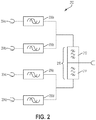
- FIG. 2 is a block diagram that depicts an example of a frequency combiner 202 followed by a low / high band combiner 210.
- Frequency combiner 202 can include input ports 204a-d, each of which can carry TX signals or RX signals of different frequencies.
- Signal-processing parameters e.g., phase shifts
- the adjustable tuning elements 206a-d can be communicatively coupled to the low / high band combiner 210.
- the low / high band combiner 210 can include a low pass filter 212 communicatively coupled to the outputs of adjustable tuning elements 206a-b.
- the low pass filter 212 filters and outputs signals below a certain threshold frequency.
- the low / high band combiner 210 can also include a high pass filter 214 communicatively coupled to the outputs of adjustable tuning elements 206c-d.
- the high pass filter 214 filters and outputs signals above a certain threshold frequency.
- the frequency combiner 202 with the low / high band combiner 210 can output adjusted signals below a certain threshold frequency and adjusted signals above a certain threshold frequency.
- each RF module 102a-d of frequency combiner 100 can include components for detecting the power difference between the signals output from the combiner component 108 with the signals input into the combiner component 108.
- the adjustable tuning elements 110a-d of the frequency combiner 100 can be tuned so that the difference in power is minimized.
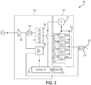
- FIG. 3 is a circuit diagram depicting an example of an RF module 301 of a frequency combiner 300 that includes circuitry for power detection and control.
- the RF module 301 can include an amplifier 302 for increasing the power of signals input into the RF module 301.
- the amplified signal can be provided to a pre-RF coupler 304, which directs the amplified signal to a duplexer 306 and a power detector component 308.
- the amplified signal can be provided through the duplexer 306 to a combiner component 320 as discussed above with respect to FIG. 1 .
- Adjustable tuning elements 316a-d can adjust signal processing parameters such that the RF path of the amplified signal is optimized for combining with signals from other RF modules (not shown).
- the combined signal can be provided to a post-RF coupler 318, which can provide the combined signal to output port 322 and to an input of the power detector component 308.
- the power detector component 308 can thus receive as inputs the signal inputted into the combiner component 320 and the combined signal output from the combiner component 320.
- a calibration process can be started within the telecommunication system to adjust the signal-processing parameters accordingly.
- a tone injection signal e.g., a test signal
- the tone injection signal can include continuous-wave (CW) tones per RF module band.
- the CW tones can be part of the TX passband of the respective RF modules, which produce a certain output power.
- the power detector component 308 of the RF module 301 can determine a difference in power between the signal inputted into the combiner component 320 (e.g., the CW tone injection signal) and the signal outputted by the combiner component 320.
- Each RF module 301 within the frequency combiner can include similar circuitry with a power detector component for comparing the difference of power levels between the signals input into the combiner component 320 with the combined signal output from the combiner component 320.
- Each power detector component 308 can provide the difference in power level to a controller 310.
- the difference in power level for each RF module 301 can also be displayed on a display device 312.
- the controller 310 can be coupled to a motor 314 or other automatic tuning element and electronically steer the motor 314 to automatically tune the adjustable tuning elements 316a-d.
- the controller 310 with the use of the motor 314, can automatically tune the signal processing parameters of the adjustable tuning elements 316a-d until the difference in power between signals input into the combiner component 320 and signals output from the combiner component 320 is minimized and optimized. By adjusting the differences in power to a minimum, the adjustable tuning elements 316a-d can be calibrated to the required needs.
- the adjustable tuning elements 316a-d can also include a manual input 324 for adjusting the signal-processing parameters of the adjustable tuning elements 316a-d, as discussed above for FIG. 1 .
- a user can manually adjust the parameters of the adjustable tuning elements 316a-d until the display device 312 indicates a minimal difference in power between the input signals and output signals.
- the display device 312 can present a user interface that can receive inputs from a user.
- the user interface on the display device 312 can receive inputs for manually adjusting and tuning the adjustable tuning elements 316a-d.
- the frequency combiners 100, 202, 300 can be implemented in a telecommunications system, such as a repeater or a DAS.
- FIG. 4 is a block diagram of an example of a repeater 400 with a frequency combiners 410a-b for combining and splitting multiple signals of varying frequencies.
- Multiple frequency bands can be received from base stations (not shown) wirelessly via one or more donor antennas 402.
- the multiple frequencies can be split into separate frequency bands and separated into transmit (TX) paths 404a-d and receive (RX) paths 406a-d using frequency combiner 410a.
- TX transmit
- RX receive
- Each of the separate TX paths 404a-d and RX paths 406a-d can carry signals on separate frequency bands.
- signal-processing components 408 can amplify signals on the TX paths 404a-d and RX paths 406a-d to a desired output power.
- Signal-processing components 408 can include, for example, analog RF components or digital signal-processing components.
- the individual TX paths 404a-d and RX paths 406a-d can be combined using frequency combiner 410b.
- the resulting combined output signal can be transmitted via one or more output ports 412 to one or more antennas or radiating cables (not shown) in order to provide signal coverage to user equipment devices positioned within the coverage zone.
- frequency combiners 100, 202, 300 can be implemented in a DAS.
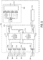
- FIG. 5 depicts an example of frequency combiners 510a-b implemented in a DAS 500.
- DAS 500 can include remote units 502a-b that include frequency combiners 510a-b according to aspects discussed herein.
- the remote units 502a-b can provide signal coverage to user equipment devices positioned within respective coverage zones.
- the remote units 502a-b can communicate with base stations 504a-e via a head-end unit 506.
- Remote units 502a-b can be communicatively coupled with head-end unit 506 via a direct wired connection or a wireless connection.
- remote units 502a-b can be communicatively coupled with head-end unit via copper cables, optical fiber, or a wireless communication medium. While FIG. 5 depicts DAS 500 with a single head-end unit 506, the DAS 500 can also include multiple head-end units.
- the head-end unit 506 can receive downlink signals from base stations 504a-e and transmit uplink signals to the base stations 504a-e. Any suitable communication link can be used for communication between the base stations 504a-e and the head-end unit 506.
- the base stations 504a-e and the head-end unit 506 can be communicatively coupled using a direct connection (e.g., copper cable or optical fiber) or a wireless communication medium.
- the head-end unit 506 can include an external repeater or internal RF transceiver to communicate with base stations 504a-e.
- Base stations 504a-e can communicate signals on multiple frequencies and on different operators with head-end unit 506.
- the head-end unit 506 can include duplexers 508a-e for providing bi-directional communication with base stations 504a-e.
- downlink signals from base station 504a can be separated from uplink signals to base station 504a via duplexer 508a.
- the downlink signals from base stations 504a-e can be provided to a splitting / combining matrix 512a. Splitting / combining matrix 512a can combine the downlink signals from base stations 504a-e to the appropriate downlink paths 514a-b intended for the respective remote units 502a-b.
- Downlink signals on downlink paths 514a-b can then be provided to optical transceivers 516a-b and then transmitted to remote units 502a-b.
- downlink signals from base stations 504a-e that are intended for remote unit 502a can be combined via splitting / combining matrix 512a and transmitted to remote unit 502a.
- downlink signals from base stations 504a-e that are intended for remote unit 502b can be combined via splitting / combining matrix 512a and transmitted to remote unit 502b.
- the downlink signals transmitted to remote units 502a-b can include signals on multiple frequencies (e.g., each base station 504a-e can transmit downlink signals on a respectively different frequency band).
- the remote units 502a-b can include frequency combiners 510a-b according to aspects described herein.
- the frequency combiners 510a-b can include adjustable tuning elements 110a-d (shown in FIG. 1 ) for adjusting the signal-processing parameters of the frequency combiners 510a-b.
- adjustable tuning elements 110a-d can adjust the phase shift of each downlink RF path to ensure that the downlink RF paths are matched optimally for combining the downlink signals and outputting the downlink signals from the remote units 502a-b.
- Implementing frequency combiners 510a-b in remote units 502a-b can allow the DAS 500 to support new frequency bands from base stations 504a-e.
- Uplink signals transmitted by user equipment devices can be received by remote units 502a-b.
- the remote units 502a-b can separate the uplink signals received from user equipment devices via frequency combiners 510a-b and transmit the separated uplink signals to head-end unit 506.
- the uplink signals from each remote unit 502a-b can be respectively provided to optical transceivers 516a-b, which can be used for bi-directional communication between head-end unit 506 and remote units 502a-b.
- the uplink signals can be provided on uplink paths 518a-b to splitting / combining matrix 512b.
- the splitting / combining matrix 512b can split the uplink signals from each remote unit 502a-b for transmittal to the appropriate base stations 504a-e.
- uplink signals from remote unit 502a may include combined signals on multiple frequency bands, signals on each frequency band intended for a respective base station 504a-e.
- Splitting / combining matrix 512b can split the uplink signals according to frequency band and direct the split uplink signals to the correct base stations 504a-e.
- the uplink signals can be provided to duplexers 508a-e and output to base stations 504a-e.
- FIGs. 4 and 5 depict block diagrams of frequency combiners being implemented in a repeater and a DAS, respectively, frequency combiners can be included in any telecommunications system.
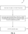
- FIG. 6 is a flowchart depicting an example process 600 for combining separate frequency bands using a frequency combiner.
- Process 600 is described with respect to the system depicted in FIG. 1 . Other implementations, however, are possible.
- Process 600 can include receiving signals at different frequencies, as shown in block 610.
- a frequency combiner 100 can include RF modules 102a-d, each RF module 102a-d tuned to receive and transmit signals on a different frequency band.
- the frequency combiner can receive signals on different frequencies via RF modules 102a-d.
- Process 600 can further include adjusting signal-processing parameters of a frequency combiner positioned between multiple input ports and an output port of a telecommunications system while the frequency combiner is in the telecommunications system, as shown in block 620.
- frequency combiner 100 can include a combiner component 108 with adjustable tuning elements 110a-d.
- the frequency combiner 100 can be positioned between input ports 104a-d that receive multiple signals on different frequencies and at least one output port 112. Signals received on each of the input ports 104a-d can be provided to RF modules 102a-d. Signals from RF modules 102a-d can be provided to adjustable tuning elements 110a-d.
- the signal-processing parameters of the frequency combiner 100 can be adjusted by automatically or manually adjusting adjustable tuning elements 110a-d.
- adjustable tuning elements 110a-d can adjust the phases of phase shifters, adjust the relative permittivity of electrical length tuners or vary the physical length of transmission lines. Thereby the phase shift of each RF path can be adjusted.
- the phase-matched RF paths allow for combining the multiple received signals in the combiner component 108 without the use of frequency-dependent multiplexers.
- the signal-processing parameters of frequency combiner can be adjusted while the frequency combiner 100 is in a telecommunications system.
- the adjustable tuning elements 102a-d can be adjusted while the frequency combiner 100 is already deployed in the field within a telecommunications system, such as a DAS or a repeater.
- the signal-processing parameter can include phase shifting or varying the electrical length of a transmission line.
- the frequency bands utilized by the telecommunications system can be upgraded while the telecommunications system is deployed in the field by exchanging the RF modules 102a-d as described above with respect to FIG. 1 .
- Process 600 can also include outputting the combined signals, as shown in block 630.
- the frequency combiner 100 can output the signals via an output port 112.
- the frequency combiner 100 can be included in a repeater unit 400 and the signals output to one or more remote units in communication with the repeater unit 400.
- the frequency combiner 100 can be included in a remote unit 502 and the signals output to one or more user equipment devices within a coverage zone of the remote unit 502.
Landscapes
- Engineering & Computer Science (AREA)
- Computer Networks & Wireless Communication (AREA)
- Signal Processing (AREA)
- Mobile Radio Communication Systems (AREA)
Claims (12)
- Système de télécommunications, comprenant :des ports d'entrée (104, 204) configurés pour recevoir des signaux radiofréquences (RF) à différentes fréquences ;au moins un port de sortie (112, 322, 412) configuré pour sortir un signal combiné ; etun combineur de fréquences (100, 202, 300, 410, 510) couplé en communication entre les ports d'entrée (104, 204) et ledit au moins un port de sortie (112, 322, 412), le combineur de fréquences (100, 202, 300, 410, 510) comportant une pluralité de modules RF (102a-d, 301) couplés en communication aux ports d'entrée, chacun de la pluralité de modules RF (102a-d, 301) comprenant un détecteur (308) avec des éléments de circuit pour déterminer les différences de niveau de puissance entre les signaux d'entrée vers le combineur de fréquences (100, 202, 300, 410, 510) et les signaux de sortie provenant du combineur de fréquences (100, 202, 300, 410, 510), le combineur de fréquences (100, 202, 300, 410, 510) comportant des éléments d'accord ajustables (110, 206, 316), chaque élément d'accord ajustable (110, 206, 316) étant configuré pour ajuster un paramètre de traitement de signal du combineur de fréquences (100, 202, 300, 410, 510) sur la base des différences déterminées de niveau de puissance, dans lequel le paramètre de traitement de signal comprend le déphasage ou la variation d'une longueur électrique d'une ligne de transmission.
- Système de télécommunications selon la revendication 1,
dans lequel le système de télécommunications est un répéteur (400) ou un système d'antennes réparties (500). - Système de télécommunications selon la revendication 1, dans lequel les éléments d'accord ajustables (110, 206, 316) sont positionnés entre ledit au moins un port de sortie (112, 322, 412) et une pluralité de duplexeurs (118, 306, 508).
- Système de télécommunications selon la revendication 1, comprenant en outre :
un contrôleur (310) couplé en communication aux détecteurs (308) et couplé en communication à des moteurs (314) dans le système de télécommunications pour amener les moteurs (314) à ajuster automatiquement les éléments d'accord ajustables (110, 206, 316) sur la base des différences de niveau de puissance. - Système de télécommunications selon la revendication 4, comprenant en outre :
un afficheur (312) configuré pour fournir une interface utilisateur pour afficher les différences de niveau de puissance entre les signaux d'entrée vers le combineur de fréquences (100, 202, 300, 410, 510) et les signaux de sortie provenant du combineur de fréquences (100, 202, 300, 410, 510). - Système de télécommunications selon la revendication 1, dans lequel chacun des éléments d'accord ajustables (110, 206, 316) est ajustable manuellement.
- Procédé, comprenant :la réception d'une pluralité de signaux radiofréquences (RF) à différentes fréquences ;l'ajustement d'un paramètre de traitement de signal d'un combineur de fréquences (100, 202, 300, 410, 510) positionné entre une pluralité de ports d'entrée (104, 204) et un port de sortie (112, 322, 412) d'un système de télécommunications en utilisant des éléments d'accord ajustables (110, 206, 316) alors que le combineur de fréquences (100, 202, 300, 410, 510) est dans le système de télécommunications ;la détermination de différences de niveau de puissance entre les signaux d'entrée vers le combineur de fréquences (100, 202, 300, 410, 510) et les signaux de sortie provenant du combineur de fréquences (100, 202, 300, 410, 510) ;l'ajustement du paramètre de traitement de signal du combineur de fréquences sur la base des différences déterminées de niveau de puissance, moyennant quoi le paramètre de traitement de signal comprend le déphasage ou la variation d'une longueur électrique d'une ligne de transmission ; etla sortie d'un signal combiné, dans lequel le combineur de fréquences (100, 202, 300, 410, 510) est indépendant de la fréquence et peut être configuré sur site.
- Procédé selon la revendication 7, dans lequel le système de télécommunications est un répéteur (400) ou un système d'antennes réparties (500).
- Procédé selon la revendication 8, comprenant en outre :
l'ajustement automatique des éléments d'accord ajustables (110, 206, 316) sur la base des différences de niveau de puissance. - Procédé selon la revendication 9, comprenant en outre :
l'affichage, sur un dispositif d'affichage (312), des différences de niveau de puissance entre les signaux d'entrée vers le combineur de fréquences (100, 202, 300, 410, 510) et les signaux de sortie provenant du combineur de fréquences (100, 202, 300, 410, 510). - Procédé selon la revendication 7, dans lequel les éléments d'accord ajustables (110, 206, 316) sont ajustés manuellement.
- Procédé selon la revendication 7, dans lequel la pluralité reçue de signaux RF sont reçus d'une unité de tête de réseau (506) d'un système d'antennes réparties (500), et dans lequel le signal combiné est transmis à un ou plusieurs dispositifs d'équipement d'utilisateur.
Priority Applications (1)
| Application Number | Priority Date | Filing Date | Title |
|---|---|---|---|
| EP20169337.1A EP3745610B1 (fr) | 2015-03-20 | 2015-10-23 | Module pour combiner des signaux présentant différentes fréquences |
Applications Claiming Priority (2)
| Application Number | Priority Date | Filing Date | Title |
|---|---|---|---|
| US201562135787P | 2015-03-20 | 2015-03-20 | |
| PCT/IB2015/058201 WO2016151376A1 (fr) | 2015-03-20 | 2015-10-23 | Module permettant de combiner des signaux de différentes fréquences |
Related Child Applications (1)
| Application Number | Title | Priority Date | Filing Date |
|---|---|---|---|
| EP20169337.1A Division EP3745610B1 (fr) | 2015-03-20 | 2015-10-23 | Module pour combiner des signaux présentant différentes fréquences |
Publications (2)
| Publication Number | Publication Date |
|---|---|
| EP3272026A1 EP3272026A1 (fr) | 2018-01-24 |
| EP3272026B1 true EP3272026B1 (fr) | 2020-04-29 |
Family
ID=54545390
Family Applications (2)
| Application Number | Title | Priority Date | Filing Date |
|---|---|---|---|
| EP15794973.6A Active EP3272026B1 (fr) | 2015-03-20 | 2015-10-23 | Module pour combinant des signaux ayant différentes fréquences |
| EP20169337.1A Active EP3745610B1 (fr) | 2015-03-20 | 2015-10-23 | Module pour combiner des signaux présentant différentes fréquences |
Family Applications After (1)
| Application Number | Title | Priority Date | Filing Date |
|---|---|---|---|
| EP20169337.1A Active EP3745610B1 (fr) | 2015-03-20 | 2015-10-23 | Module pour combiner des signaux présentant différentes fréquences |
Country Status (4)
| Country | Link |
|---|---|
| US (1) | US10212018B2 (fr) |
| EP (2) | EP3272026B1 (fr) |
| CN (1) | CN107210758B (fr) |
| WO (1) | WO2016151376A1 (fr) |
Families Citing this family (6)
| Publication number | Priority date | Publication date | Assignee | Title |
|---|---|---|---|---|
| KR102417238B1 (ko) * | 2016-04-13 | 2022-07-06 | 주식회사 쏠리드 | 분산 안테나 시스템 및 그 신호 처리 방법 |
| EP3921891B1 (fr) * | 2019-02-06 | 2024-04-24 | Andrew Wireless Systems GmbH | Système de filtre/duplexeur modulaire |
| WO2022098660A1 (fr) | 2020-11-09 | 2022-05-12 | Commscope Technologies Llc | Système de filtre/duplexeur modulaire à bande large |
| WO2022153311A1 (fr) | 2021-01-17 | 2022-07-21 | Rospsha Nimrod | Multiplexeur actif |
| CN113626715A (zh) * | 2021-08-26 | 2021-11-09 | 北京字跳网络技术有限公司 | 查询结果显示方法、装置、介质和电子设备 |
| US12143145B2 (en) * | 2022-09-07 | 2024-11-12 | Apple Inc. | Duplexer measurement and tuning systems |
Family Cites Families (31)
| Publication number | Priority date | Publication date | Assignee | Title |
|---|---|---|---|---|
| US5838675A (en) * | 1996-07-03 | 1998-11-17 | The United States Of America As Represented By The Secretary Of The Navy | Channelized receiver-front-end protection circuit which demultiplexes broadband signals into a plurality of different microwave signals in respective contiguous frequency channels, phase adjusts and multiplexes channels |
| JP2001305439A (ja) * | 2000-04-24 | 2001-10-31 | Seiko Instruments Inc | 光通信機器 |
| US20030107517A1 (en) * | 2001-12-10 | 2003-06-12 | Tdk Corporation | Antenna beam control system |
| WO2004038973A1 (fr) * | 2002-10-23 | 2004-05-06 | Hitachi Kokusai Electric Inc. | Emetteur |
| US7586886B2 (en) * | 2004-10-06 | 2009-09-08 | Broadcom Corporation | Method and system for single weight antenna system for HSDPA |
| US8280309B2 (en) * | 2005-04-08 | 2012-10-02 | The Boeing Company | Soft handoff method and apparatus for mobile vehicles using directional antennas |
| JP4558565B2 (ja) * | 2005-04-14 | 2010-10-06 | 古河電気工業株式会社 | 光波形成形器及び該光波形成形器を用いた光信号発生器 |
| JP4772574B2 (ja) * | 2006-04-14 | 2011-09-14 | 株式会社東芝 | 増幅器および無線通信回路 |
| US7894779B2 (en) * | 2006-06-22 | 2011-02-22 | Honeywell International Inc. | Apparatus and method for transmitting and receiving multiple radio signals over a single antenna |
| CN1917377B (zh) * | 2006-07-14 | 2010-10-06 | 镇江蓝宝石电子实业有限公司 | 一种远端控制自调谐合路器 |
| US7612612B2 (en) * | 2007-06-22 | 2009-11-03 | Texas Instruments Incorporated | Calibration circuitry and delay cells in rectilinear RF power amplifier |
| US8576946B2 (en) * | 2007-10-19 | 2013-11-05 | Trellisware Technologies, Inc. | Method and system for cooperative communications with minimal coordination |
| EP2353219B1 (fr) * | 2008-11-11 | 2018-05-02 | Massachusetts Institute of Technology | Architecture de déphasage à niveaux multiples asymétrique pour amplificateurs rf |
| CN101859920A (zh) * | 2009-04-08 | 2010-10-13 | 深圳市信特科技有限公司 | 一种八合一自动调谐空腔合路器 |
| US20110249831A1 (en) * | 2010-04-13 | 2011-10-13 | Bellamy David C | Wireless microphone systems having improved immunity to rf interference |
| CN201752030U (zh) * | 2010-07-15 | 2011-02-23 | 北京东方信联科技有限公司 | 一种合路器 |
| US8537912B2 (en) * | 2011-02-24 | 2013-09-17 | Futurewei Technologies, Inc. | Extremely high speed broadband access over copper pairs |
| US20130109325A1 (en) * | 2011-10-28 | 2013-05-02 | Broadcom Corporation | Dual mode local area network transceiver and methods for use therewith |
| CN102594749A (zh) * | 2012-02-28 | 2012-07-18 | 中兴通讯股份有限公司 | 一种数字预失真处理方法及装置 |
| US8885757B2 (en) * | 2012-05-29 | 2014-11-11 | Magnolia Broadband Inc. | Calibration of MIMO systems with radio distribution networks |
| EP2856654A4 (fr) * | 2012-06-05 | 2016-03-09 | Rivada Networks Llc | Procédé et système pour fournir une agrégation de porteuses multiples diverses |
| JP5906967B2 (ja) * | 2012-06-29 | 2016-04-20 | 富士通株式会社 | 歪補償装置および歪補償方法 |
| JP5646553B2 (ja) * | 2012-07-06 | 2014-12-24 | 株式会社東芝 | アンテナユニット |
| KR101941079B1 (ko) * | 2012-09-28 | 2019-01-23 | 삼성전자주식회사 | 전력 결합 장치에서의 출력 특성 보정장치 및 방법 |
| US8805297B2 (en) * | 2012-10-16 | 2014-08-12 | Raytheon Company | Band stitching electronic circuits and techniques |
| US9166536B2 (en) * | 2012-10-30 | 2015-10-20 | Eta Devices, Inc. | Transmitter architecture and related methods |
| US8824978B2 (en) * | 2012-10-30 | 2014-09-02 | Eta Devices, Inc. | RF amplifier architecture and related techniques |
| WO2014112040A1 (fr) * | 2013-01-15 | 2014-07-24 | 三菱電機株式会社 | Satellite relais, dispositif de relais, et système de communication par satellite |
| US9923621B2 (en) * | 2013-02-16 | 2018-03-20 | Cable Television Laboratories, Inc. | Multiple-input multiple-output (MIMO) communication system |
| WO2014185459A1 (fr) * | 2013-05-16 | 2014-11-20 | 日本電気株式会社 | Dispositif de transmission et procédé de transmission |
| JP6242311B2 (ja) * | 2013-10-29 | 2017-12-06 | パナソニック株式会社 | 無線送電装置及び無線電力伝送システム |
-
2015
- 2015-10-23 EP EP15794973.6A patent/EP3272026B1/fr active Active
- 2015-10-23 WO PCT/IB2015/058201 patent/WO2016151376A1/fr not_active Ceased
- 2015-10-23 US US15/559,795 patent/US10212018B2/en active Active
- 2015-10-23 CN CN201580075460.3A patent/CN107210758B/zh not_active Expired - Fee Related
- 2015-10-23 EP EP20169337.1A patent/EP3745610B1/fr active Active
Non-Patent Citations (1)
| Title |
|---|
| None * |
Also Published As
| Publication number | Publication date |
|---|---|
| EP3745610A1 (fr) | 2020-12-02 |
| CN107210758A (zh) | 2017-09-26 |
| WO2016151376A1 (fr) | 2016-09-29 |
| US10212018B2 (en) | 2019-02-19 |
| EP3745610B1 (fr) | 2022-12-28 |
| US20180069741A1 (en) | 2018-03-08 |
| EP3272026A1 (fr) | 2018-01-24 |
| CN107210758B (zh) | 2020-03-03 |
Similar Documents
| Publication | Publication Date | Title |
|---|---|---|
| EP3272026B1 (fr) | Module pour combinant des signaux ayant différentes fréquences | |
| EP3632006B1 (fr) | Extension de la dynamique de détection de signaux tdd et extension de la robustesse vis-à-vis de signaux volatils | |
| EP2159933B1 (fr) | Réglage d'amplificateurs dans un système distribué d'antennes | |
| EP2433377B2 (fr) | Système de distribution de signaux radioélectriques | |
| EP3369131B1 (fr) | Cartes de circuit imprimé d'étalonnage et systèmes d'antennes intégrées associés à isolation inter-bande améliorée | |
| EP2030328B1 (fr) | Appareil et procédé pour transmettre et recevoir des signaux radio multiples sur une antenne unique | |
| EP3145090B1 (fr) | Dispositif d'antenne active, système de communication, et procédé d'étalonnage d'émission et de réception | |
| US9882613B2 (en) | Determining actual loop gain in a distributed antenna system (DAS) | |
| EP2980990B1 (fr) | Amplificateur de puissance | |
| EP1227605A3 (fr) | Procédé et dispositif de distribution de signaux multibandes de communication sans fil | |
| US20110267976A1 (en) | Wireless relay apparatus and wireless relay system | |
| US20120052819A1 (en) | Radio communication device and radio communication method | |
| KR101868965B1 (ko) | 분산 안테나 시스템의 리모트 장치 | |
| KR101415540B1 (ko) | 대역별 가변틸트 안테나 장치 | |
| JP6045296B2 (ja) | Rfフロントエンドモジュール | |
| US11601145B2 (en) | Tunable antenna and communications terminal | |
| KR102019082B1 (ko) | 밀리미터파 빔포밍을 위한 4채널 위상 정밀 제어 장치 | |
| EP1995879B1 (fr) | Station de base et procédé de transmission | |
| US20240305329A1 (en) | Systems and methods for signal path isolation for neutral-host hardware | |
| EP2777092B1 (fr) | Appareil de combinaison pour utilisation dans un appareil d'émission et/ou de réception de signal | |
| US11204380B2 (en) | Module tuning using virtual gain correction | |
| WO2017158910A1 (fr) | Système d'antenne active | |
| KR200277318Y1 (ko) | 다이버시티 신호 합성/분배기 | |
| JP2007158973A (ja) | 移動体通信端末 | |
| HK40036013A (en) | Adjustable antenna and communication terminal |
Legal Events
| Date | Code | Title | Description |
|---|---|---|---|
| STAA | Information on the status of an ep patent application or granted ep patent |
Free format text: STATUS: THE INTERNATIONAL PUBLICATION HAS BEEN MADE |
|
| PUAI | Public reference made under article 153(3) epc to a published international application that has entered the european phase |
Free format text: ORIGINAL CODE: 0009012 |
|
| STAA | Information on the status of an ep patent application or granted ep patent |
Free format text: STATUS: REQUEST FOR EXAMINATION WAS MADE |
|
| 17P | Request for examination filed |
Effective date: 20170704 |
|
| AK | Designated contracting states |
Kind code of ref document: A1 Designated state(s): AL AT BE BG CH CY CZ DE DK EE ES FI FR GB GR HR HU IE IS IT LI LT LU LV MC MK MT NL NO PL PT RO RS SE SI SK SM TR |
|
| AX | Request for extension of the european patent |
Extension state: BA ME |
|
| DAV | Request for validation of the european patent (deleted) | ||
| DAX | Request for extension of the european patent (deleted) | ||
| GRAP | Despatch of communication of intention to grant a patent |
Free format text: ORIGINAL CODE: EPIDOSNIGR1 |
|
| STAA | Information on the status of an ep patent application or granted ep patent |
Free format text: STATUS: GRANT OF PATENT IS INTENDED |
|
| INTG | Intention to grant announced |
Effective date: 20191119 |
|
| RIN1 | Information on inventor provided before grant (corrected) |
Inventor name: FACKLER, KARL-HEINZ Inventor name: SCHMID, PETER Inventor name: KUMMETZ, THOMAS Inventor name: DUSSMANN, ALFONS Inventor name: HOFMAN, ROMAN |
|
| GRAS | Grant fee paid |
Free format text: ORIGINAL CODE: EPIDOSNIGR3 |
|
| GRAA | (expected) grant |
Free format text: ORIGINAL CODE: 0009210 |
|
| STAA | Information on the status of an ep patent application or granted ep patent |
Free format text: STATUS: THE PATENT HAS BEEN GRANTED |
|
| AK | Designated contracting states |
Kind code of ref document: B1 Designated state(s): AL AT BE BG CH CY CZ DE DK EE ES FI FR GB GR HR HU IE IS IT LI LT LU LV MC MK MT NL NO PL PT RO RS SE SI SK SM TR |
|
| REG | Reference to a national code |
Ref country code: GB Ref legal event code: FG4D |
|
| REG | Reference to a national code |
Ref country code: CH Ref legal event code: EP |
|
| REG | Reference to a national code |
Ref country code: AT Ref legal event code: REF Ref document number: 1264871 Country of ref document: AT Kind code of ref document: T Effective date: 20200515 |
|
| REG | Reference to a national code |
Ref country code: DE Ref legal event code: R096 Ref document number: 602015051748 Country of ref document: DE |
|
| REG | Reference to a national code |
Ref country code: IE Ref legal event code: FG4D |
|
| REG | Reference to a national code |
Ref country code: NL Ref legal event code: FP |
|
| REG | Reference to a national code |
Ref country code: LT Ref legal event code: MG4D |
|
| PG25 | Lapsed in a contracting state [announced via postgrant information from national office to epo] |
Ref country code: SE Free format text: LAPSE BECAUSE OF FAILURE TO SUBMIT A TRANSLATION OF THE DESCRIPTION OR TO PAY THE FEE WITHIN THE PRESCRIBED TIME-LIMIT Effective date: 20200429 Ref country code: LT Free format text: LAPSE BECAUSE OF FAILURE TO SUBMIT A TRANSLATION OF THE DESCRIPTION OR TO PAY THE FEE WITHIN THE PRESCRIBED TIME-LIMIT Effective date: 20200429 Ref country code: PT Free format text: LAPSE BECAUSE OF FAILURE TO SUBMIT A TRANSLATION OF THE DESCRIPTION OR TO PAY THE FEE WITHIN THE PRESCRIBED TIME-LIMIT Effective date: 20200831 Ref country code: IS Free format text: LAPSE BECAUSE OF FAILURE TO SUBMIT A TRANSLATION OF THE DESCRIPTION OR TO PAY THE FEE WITHIN THE PRESCRIBED TIME-LIMIT Effective date: 20200829 Ref country code: GR Free format text: LAPSE BECAUSE OF FAILURE TO SUBMIT A TRANSLATION OF THE DESCRIPTION OR TO PAY THE FEE WITHIN THE PRESCRIBED TIME-LIMIT Effective date: 20200730 Ref country code: FI Free format text: LAPSE BECAUSE OF FAILURE TO SUBMIT A TRANSLATION OF THE DESCRIPTION OR TO PAY THE FEE WITHIN THE PRESCRIBED TIME-LIMIT Effective date: 20200429 Ref country code: NO Free format text: LAPSE BECAUSE OF FAILURE TO SUBMIT A TRANSLATION OF THE DESCRIPTION OR TO PAY THE FEE WITHIN THE PRESCRIBED TIME-LIMIT Effective date: 20200729 |
|
| REG | Reference to a national code |
Ref country code: AT Ref legal event code: MK05 Ref document number: 1264871 Country of ref document: AT Kind code of ref document: T Effective date: 20200429 |
|
| PG25 | Lapsed in a contracting state [announced via postgrant information from national office to epo] |
Ref country code: HR Free format text: LAPSE BECAUSE OF FAILURE TO SUBMIT A TRANSLATION OF THE DESCRIPTION OR TO PAY THE FEE WITHIN THE PRESCRIBED TIME-LIMIT Effective date: 20200429 Ref country code: LV Free format text: LAPSE BECAUSE OF FAILURE TO SUBMIT A TRANSLATION OF THE DESCRIPTION OR TO PAY THE FEE WITHIN THE PRESCRIBED TIME-LIMIT Effective date: 20200429 Ref country code: BG Free format text: LAPSE BECAUSE OF FAILURE TO SUBMIT A TRANSLATION OF THE DESCRIPTION OR TO PAY THE FEE WITHIN THE PRESCRIBED TIME-LIMIT Effective date: 20200729 Ref country code: RS Free format text: LAPSE BECAUSE OF FAILURE TO SUBMIT A TRANSLATION OF THE DESCRIPTION OR TO PAY THE FEE WITHIN THE PRESCRIBED TIME-LIMIT Effective date: 20200429 |
|
| PG25 | Lapsed in a contracting state [announced via postgrant information from national office to epo] |
Ref country code: AL Free format text: LAPSE BECAUSE OF FAILURE TO SUBMIT A TRANSLATION OF THE DESCRIPTION OR TO PAY THE FEE WITHIN THE PRESCRIBED TIME-LIMIT Effective date: 20200429 |
|
| PG25 | Lapsed in a contracting state [announced via postgrant information from national office to epo] |
Ref country code: CZ Free format text: LAPSE BECAUSE OF FAILURE TO SUBMIT A TRANSLATION OF THE DESCRIPTION OR TO PAY THE FEE WITHIN THE PRESCRIBED TIME-LIMIT Effective date: 20200429 Ref country code: RO Free format text: LAPSE BECAUSE OF FAILURE TO SUBMIT A TRANSLATION OF THE DESCRIPTION OR TO PAY THE FEE WITHIN THE PRESCRIBED TIME-LIMIT Effective date: 20200429 Ref country code: ES Free format text: LAPSE BECAUSE OF FAILURE TO SUBMIT A TRANSLATION OF THE DESCRIPTION OR TO PAY THE FEE WITHIN THE PRESCRIBED TIME-LIMIT Effective date: 20200429 Ref country code: AT Free format text: LAPSE BECAUSE OF FAILURE TO SUBMIT A TRANSLATION OF THE DESCRIPTION OR TO PAY THE FEE WITHIN THE PRESCRIBED TIME-LIMIT Effective date: 20200429 Ref country code: EE Free format text: LAPSE BECAUSE OF FAILURE TO SUBMIT A TRANSLATION OF THE DESCRIPTION OR TO PAY THE FEE WITHIN THE PRESCRIBED TIME-LIMIT Effective date: 20200429 Ref country code: SM Free format text: LAPSE BECAUSE OF FAILURE TO SUBMIT A TRANSLATION OF THE DESCRIPTION OR TO PAY THE FEE WITHIN THE PRESCRIBED TIME-LIMIT Effective date: 20200429 Ref country code: DK Free format text: LAPSE BECAUSE OF FAILURE TO SUBMIT A TRANSLATION OF THE DESCRIPTION OR TO PAY THE FEE WITHIN THE PRESCRIBED TIME-LIMIT Effective date: 20200429 |
|
| REG | Reference to a national code |
Ref country code: DE Ref legal event code: R097 Ref document number: 602015051748 Country of ref document: DE |
|
| PG25 | Lapsed in a contracting state [announced via postgrant information from national office to epo] |
Ref country code: SK Free format text: LAPSE BECAUSE OF FAILURE TO SUBMIT A TRANSLATION OF THE DESCRIPTION OR TO PAY THE FEE WITHIN THE PRESCRIBED TIME-LIMIT Effective date: 20200429 Ref country code: PL Free format text: LAPSE BECAUSE OF FAILURE TO SUBMIT A TRANSLATION OF THE DESCRIPTION OR TO PAY THE FEE WITHIN THE PRESCRIBED TIME-LIMIT Effective date: 20200429 |
|
| PLBE | No opposition filed within time limit |
Free format text: ORIGINAL CODE: 0009261 |
|
| STAA | Information on the status of an ep patent application or granted ep patent |
Free format text: STATUS: NO OPPOSITION FILED WITHIN TIME LIMIT |
|
| 26N | No opposition filed |
Effective date: 20210201 |
|
| PG25 | Lapsed in a contracting state [announced via postgrant information from national office to epo] |
Ref country code: SI Free format text: LAPSE BECAUSE OF FAILURE TO SUBMIT A TRANSLATION OF THE DESCRIPTION OR TO PAY THE FEE WITHIN THE PRESCRIBED TIME-LIMIT Effective date: 20200429 |
|
| REG | Reference to a national code |
Ref country code: CH Ref legal event code: PL |
|
| GBPC | Gb: european patent ceased through non-payment of renewal fee |
Effective date: 20201023 |
|
| PG25 | Lapsed in a contracting state [announced via postgrant information from national office to epo] |
Ref country code: MC Free format text: LAPSE BECAUSE OF FAILURE TO SUBMIT A TRANSLATION OF THE DESCRIPTION OR TO PAY THE FEE WITHIN THE PRESCRIBED TIME-LIMIT Effective date: 20200429 Ref country code: LU Free format text: LAPSE BECAUSE OF NON-PAYMENT OF DUE FEES Effective date: 20201023 |
|
| REG | Reference to a national code |
Ref country code: BE Ref legal event code: MM Effective date: 20201031 |
|
| PG25 | Lapsed in a contracting state [announced via postgrant information from national office to epo] |
Ref country code: CH Free format text: LAPSE BECAUSE OF NON-PAYMENT OF DUE FEES Effective date: 20201031 Ref country code: BE Free format text: LAPSE BECAUSE OF NON-PAYMENT OF DUE FEES Effective date: 20201031 Ref country code: GB Free format text: LAPSE BECAUSE OF NON-PAYMENT OF DUE FEES Effective date: 20201023 Ref country code: LI Free format text: LAPSE BECAUSE OF NON-PAYMENT OF DUE FEES Effective date: 20201031 |
|
| PG25 | Lapsed in a contracting state [announced via postgrant information from national office to epo] |
Ref country code: IE Free format text: LAPSE BECAUSE OF NON-PAYMENT OF DUE FEES Effective date: 20201023 |
|
| PG25 | Lapsed in a contracting state [announced via postgrant information from national office to epo] |
Ref country code: TR Free format text: LAPSE BECAUSE OF FAILURE TO SUBMIT A TRANSLATION OF THE DESCRIPTION OR TO PAY THE FEE WITHIN THE PRESCRIBED TIME-LIMIT Effective date: 20200429 Ref country code: MT Free format text: LAPSE BECAUSE OF FAILURE TO SUBMIT A TRANSLATION OF THE DESCRIPTION OR TO PAY THE FEE WITHIN THE PRESCRIBED TIME-LIMIT Effective date: 20200429 Ref country code: CY Free format text: LAPSE BECAUSE OF FAILURE TO SUBMIT A TRANSLATION OF THE DESCRIPTION OR TO PAY THE FEE WITHIN THE PRESCRIBED TIME-LIMIT Effective date: 20200429 |
|
| PG25 | Lapsed in a contracting state [announced via postgrant information from national office to epo] |
Ref country code: MK Free format text: LAPSE BECAUSE OF FAILURE TO SUBMIT A TRANSLATION OF THE DESCRIPTION OR TO PAY THE FEE WITHIN THE PRESCRIBED TIME-LIMIT Effective date: 20200429 |
|
| P01 | Opt-out of the competence of the unified patent court (upc) registered |
Effective date: 20230530 |
|
| PGFP | Annual fee paid to national office [announced via postgrant information from national office to epo] |
Ref country code: NL Payment date: 20231026 Year of fee payment: 9 |
|
| PGFP | Annual fee paid to national office [announced via postgrant information from national office to epo] |
Ref country code: IT Payment date: 20231023 Year of fee payment: 9 Ref country code: FR Payment date: 20231025 Year of fee payment: 9 Ref country code: DE Payment date: 20231027 Year of fee payment: 9 |
|
| REG | Reference to a national code |
Ref country code: DE Ref legal event code: R119 Ref document number: 602015051748 Country of ref document: DE |
|
| REG | Reference to a national code |
Ref country code: NL Ref legal event code: MM Effective date: 20241101 |
|
| PG25 | Lapsed in a contracting state [announced via postgrant information from national office to epo] |
Ref country code: DE Free format text: LAPSE BECAUSE OF NON-PAYMENT OF DUE FEES Effective date: 20250501 |
|
| PG25 | Lapsed in a contracting state [announced via postgrant information from national office to epo] |
Ref country code: NL Free format text: LAPSE BECAUSE OF NON-PAYMENT OF DUE FEES Effective date: 20241101 |
|
| PG25 | Lapsed in a contracting state [announced via postgrant information from national office to epo] |
Ref country code: FR Free format text: LAPSE BECAUSE OF NON-PAYMENT OF DUE FEES Effective date: 20241031 |
|
| PG25 | Lapsed in a contracting state [announced via postgrant information from national office to epo] |
Ref country code: IT Free format text: LAPSE BECAUSE OF NON-PAYMENT OF DUE FEES Effective date: 20241023 |