EP3300108B1 - Lichtemittierende vorrichtung und verfahren zur herstellung davon - Google Patents
Lichtemittierende vorrichtung und verfahren zur herstellung davon Download PDFInfo
- Publication number
- EP3300108B1 EP3300108B1 EP17199755.4A EP17199755A EP3300108B1 EP 3300108 B1 EP3300108 B1 EP 3300108B1 EP 17199755 A EP17199755 A EP 17199755A EP 3300108 B1 EP3300108 B1 EP 3300108B1
- Authority
- EP
- European Patent Office
- Prior art keywords
- light transmissive
- light emitting
- conductive circuit
- circuit layer
- light
- Prior art date
- Legal status (The legal status is an assumption and is not a legal conclusion. Google has not performed a legal analysis and makes no representation as to the accuracy of the status listed.)
- Active
Links
Images


Classifications
-
- H—ELECTRICITY
- H10—SEMICONDUCTOR DEVICES; ELECTRIC SOLID-STATE DEVICES NOT OTHERWISE PROVIDED FOR
- H10H—INORGANIC LIGHT-EMITTING SEMICONDUCTOR DEVICES HAVING POTENTIAL BARRIERS
- H10H20/00—Individual inorganic light-emitting semiconductor devices having potential barriers, e.g. light-emitting diodes [LED]
- H10H20/80—Constructional details
- H10H20/85—Packages
- H10H20/852—Encapsulations
- H10H20/854—Encapsulations characterised by their material, e.g. epoxy or silicone resins
-
- H—ELECTRICITY
- H10—SEMICONDUCTOR DEVICES; ELECTRIC SOLID-STATE DEVICES NOT OTHERWISE PROVIDED FOR
- H10H—INORGANIC LIGHT-EMITTING SEMICONDUCTOR DEVICES HAVING POTENTIAL BARRIERS
- H10H20/00—Individual inorganic light-emitting semiconductor devices having potential barriers, e.g. light-emitting diodes [LED]
- H10H20/80—Constructional details
- H10H20/85—Packages
- H10H20/852—Encapsulations
- H10H20/853—Encapsulations characterised by their shape
-
- H—ELECTRICITY
- H10—SEMICONDUCTOR DEVICES; ELECTRIC SOLID-STATE DEVICES NOT OTHERWISE PROVIDED FOR
- H10H—INORGANIC LIGHT-EMITTING SEMICONDUCTOR DEVICES HAVING POTENTIAL BARRIERS
- H10H29/00—Integrated devices, or assemblies of multiple devices, comprising at least one light-emitting semiconductor element covered by group H10H20/00
- H10H29/10—Integrated devices comprising at least one light-emitting semiconductor component covered by group H10H20/00
- H10H29/14—Integrated devices comprising at least one light-emitting semiconductor component covered by group H10H20/00 comprising multiple light-emitting semiconductor components
- H10H29/142—Two-dimensional arrangements, e.g. asymmetric LED layout
-
- H—ELECTRICITY
- H10—SEMICONDUCTOR DEVICES; ELECTRIC SOLID-STATE DEVICES NOT OTHERWISE PROVIDED FOR
- H10W—GENERIC PACKAGES, INTERCONNECTIONS, CONNECTORS OR OTHER CONSTRUCTIONAL DETAILS OF DEVICES COVERED BY CLASS H10
- H10W70/00—Package substrates; Interposers; Redistribution layers [RDL]
- H10W70/01—Manufacture or treatment
- H10W70/05—Manufacture or treatment of insulating or insulated package substrates, or of interposers, or of redistribution layers
- H10W70/08—Manufacture or treatment of insulating or insulated package substrates, or of interposers, or of redistribution layers by depositing layers on the chip or wafer, e.g. "chip-first" RDLs
- H10W70/09—Manufacture or treatment of insulating or insulated package substrates, or of interposers, or of redistribution layers by depositing layers on the chip or wafer, e.g. "chip-first" RDLs extending onto an encapsulation that laterally surrounds the chip or wafer, e.g. fan-out wafer level package [FOWLP] RDLs
-
- H—ELECTRICITY
- H10—SEMICONDUCTOR DEVICES; ELECTRIC SOLID-STATE DEVICES NOT OTHERWISE PROVIDED FOR
- H10W—GENERIC PACKAGES, INTERCONNECTIONS, CONNECTORS OR OTHER CONSTRUCTIONAL DETAILS OF DEVICES COVERED BY CLASS H10
- H10W70/00—Package substrates; Interposers; Redistribution layers [RDL]
- H10W70/60—Insulating or insulated package substrates; Interposers; Redistribution layers
-
- H—ELECTRICITY
- H10—SEMICONDUCTOR DEVICES; ELECTRIC SOLID-STATE DEVICES NOT OTHERWISE PROVIDED FOR
- H10W—GENERIC PACKAGES, INTERCONNECTIONS, CONNECTORS OR OTHER CONSTRUCTIONAL DETAILS OF DEVICES COVERED BY CLASS H10
- H10W90/00—Package configurations
-
- H—ELECTRICITY
- H10—SEMICONDUCTOR DEVICES; ELECTRIC SOLID-STATE DEVICES NOT OTHERWISE PROVIDED FOR
- H10H—INORGANIC LIGHT-EMITTING SEMICONDUCTOR DEVICES HAVING POTENTIAL BARRIERS
- H10H20/00—Individual inorganic light-emitting semiconductor devices having potential barriers, e.g. light-emitting diodes [LED]
- H10H20/01—Manufacture or treatment
- H10H20/036—Manufacture or treatment of packages
- H10H20/0362—Manufacture or treatment of packages of encapsulations
-
- H—ELECTRICITY
- H10—SEMICONDUCTOR DEVICES; ELECTRIC SOLID-STATE DEVICES NOT OTHERWISE PROVIDED FOR
- H10H—INORGANIC LIGHT-EMITTING SEMICONDUCTOR DEVICES HAVING POTENTIAL BARRIERS
- H10H20/00—Individual inorganic light-emitting semiconductor devices having potential barriers, e.g. light-emitting diodes [LED]
- H10H20/80—Constructional details
- H10H20/85—Packages
- H10H20/857—Interconnections, e.g. lead-frames, bond wires or solder balls
-
- H—ELECTRICITY
- H10—SEMICONDUCTOR DEVICES; ELECTRIC SOLID-STATE DEVICES NOT OTHERWISE PROVIDED FOR
- H10W—GENERIC PACKAGES, INTERCONNECTIONS, CONNECTORS OR OTHER CONSTRUCTIONAL DETAILS OF DEVICES COVERED BY CLASS H10
- H10W70/00—Package substrates; Interposers; Redistribution layers [RDL]
- H10W70/099—Connecting interconnections to insulating or insulated package substrates, interposers or redistribution layers
-
- H—ELECTRICITY
- H10—SEMICONDUCTOR DEVICES; ELECTRIC SOLID-STATE DEVICES NOT OTHERWISE PROVIDED FOR
- H10W—GENERIC PACKAGES, INTERCONNECTIONS, CONNECTORS OR OTHER CONSTRUCTIONAL DETAILS OF DEVICES COVERED BY CLASS H10
- H10W72/00—Interconnections or connectors in packages
- H10W72/071—Connecting or disconnecting
- H10W72/073—Connecting or disconnecting of die-attach connectors
-
- H—ELECTRICITY
- H10—SEMICONDUCTOR DEVICES; ELECTRIC SOLID-STATE DEVICES NOT OTHERWISE PROVIDED FOR
- H10W—GENERIC PACKAGES, INTERCONNECTIONS, CONNECTORS OR OTHER CONSTRUCTIONAL DETAILS OF DEVICES COVERED BY CLASS H10
- H10W72/00—Interconnections or connectors in packages
- H10W72/851—Dispositions of multiple connectors or interconnections
- H10W72/874—On different surfaces
-
- H—ELECTRICITY
- H10—SEMICONDUCTOR DEVICES; ELECTRIC SOLID-STATE DEVICES NOT OTHERWISE PROVIDED FOR
- H10W—GENERIC PACKAGES, INTERCONNECTIONS, CONNECTORS OR OTHER CONSTRUCTIONAL DETAILS OF DEVICES COVERED BY CLASS H10
- H10W90/00—Package configurations
- H10W90/10—Configurations of laterally-adjacent chips
Definitions
- Embodiments described herein relate generally to a light emitting device and a method for manufacturing the same.
- a light emitting device using a light emitting diode is widely used for optical devices such as indoor, outdoor, stationary, mobile display devices, display lamps, various switches, signal devices, general lightings and so on.
- a transparent light emitting device is known in which a plurality of LEDs are arranged between two transparent substrates.
- Using a flexible substrate made of a transparent resin as the transparent substrate eases the constraint on the attachment surface of the light emitting device as the display device or the display lamp, resulting in improved convenience and availability of the transparent light emitting device.
- the transparent light emitting device has a structure in which a plurality of LED chips are arranged, for example, between a first transparent insulating substrate having a first conductive circuit layer and a second transparent insulating substrate having a second conductive circuit layer.
- Each of the plurality of LED chips has a pair of electrodes. One of the electrodes is electrically connected to the first conductive circuit layer, and the other electrode is electrically connected to the second conductive circuit layer.
- the plurality of LED chips are arranged with a certain interval therebetween.
- a transparent insulator made of a transparent resin or the like having electric insulation property and bendability is filled.
- the LED chips are arranged in through holes provided in the transparent insulator.
- the electrical connection between the electrodes of the LED chips and the conductive circuit layers in the transparent light emitting device is sometimes made, for example, by vacuum thermocompression bonding a stack composed of the first transparent insulating substrate, a transparent insulating resin sheet in which the LED chips are arranged in the through holes, and the second transparent insulating substrate.
- the electrodes of the LED chips and the conductive circuit layers are sometimes bonded with each other with a conductive adhesive.
- thermocompression bonding is performed with a hot melt adhesive sheet, to which the LED chips are fixed, sandwiched between upper and lower insulating substrates having the conductive circuit layers to embed the LED chips in the adhesive sheet, thereby performing the bonding of the upper and lower insulating substrates and the electrical connection between the electrodes of the LED chips and the conductive circuit layers at the same time.
- the thickness of the transparent insulating resin sheet after the thermocompression bonding (the thickness of the transparent insulator) is made smaller than the thickness of the LED chip to press the conductive circuit layers against the electrodes of the LED chips so as to bring them into contact
- the thickness of the transparent insulator or the arrangement interval of the LED chips it is impossible to reliably electrically connect the electrodes and the conductive circuit layers.
- An object to be solved by the present invention is to provide a light emitting device and a method for manufacturing the same, in which the electrical connection between a conductive circuit layer provided on the surface of a light transmissive insulator and an electrode of an LED chip and its reliability can be increased with high reproducibility.
- a light emitting device in an embodiment includes: a first light transmissive support including a first light transmissive insulator; a second light transmissive support including a second light transmissive insulator; a conductive circuit layer provided on at least one of a first surface of the first light transmissive insulator and a second surface of the second light transmissive insulator opposed to the first surface; a light emitting diode including: a light emitting diode body having a first face and a second face; a first electrode provided on the first face of the light emitting diode body and electrically connected to the conductive circuit layer; and a second electrode provided on the first face or the second face of the light emitting diode body and electrically connected to the conductive circuit layer, and arranged between the first light transmissive insulator and the second light transmissive insulator; and a third light transmissive insulator embedded between the first light transmissive insulator and the second light transmissive insulator and having at least one of a
- a method for manufacturing a light emitting device in an embodiment includes: preparing a first light transmissive support including a first light transmissive insulator, and a second light transmissive support including a second light transmissive insulator, forming a conductive circuit layer on at least one of a first surface of the first light transmissive insulator and a second surface of the second light transmissive insulator, preparing a light emitting diode including a light emitting diode body having a first face and a second face, a first electrode provided on the first face of the light emitting diode body, and a second electrode provided on the first face or the second face of the light emitting diode body; arranging a light transmissive insulating resin sheet having at least one of a Vicat softening temperature of 80°C or higher and 160°C or lower and a tensile storage elastic modulus of 0.01 GPa or more and 10 GPa or less on the surface, on which the conductive circuit layer is provided, of
- FIG. 1 is a cross-sectional view illustrating a configuration of a light emitting device according to a first embodiment.
- a light emitting device 1 illustrated in Fig. 1 includes a first light transmissive support 2 and a second light transmissive support 3.
- the first light transmissive support 2 includes a first light transmissive insulator 4 and a first conductive circuit layer 5 formed on the surface of the first light transmissive insulator 4.
- the second light transmissive support 3 includes a second light transmissive insulator 6 and a second conductive circuit layer 7 formed on the surface of the second light transmissive insulator 6.
- the first light transmissive support 2 and the second light transmissive support 3 are arranged with a predetermined gap provided therebetween such that the first conductive circuit layer 5 and the second conductive circuit layer 7 are opposed to each other.
- a plurality of light emitting diodes 8 are arranged in the gap between the first light transmissive support 2 and the second light transmissive support 3.
- the light transmissive insulators 4, 6, for example, a resin material having an insulation property and a light transmitting property is used, and a resin material further having flexibility is preferably used.
- an insulating resin material include polyethylene terephthalate (PET), polyethylene naphthalate (PEN), polycarbonate (PC), polyethylene succinate (PES), cyclic olefin resin (for example, ARTON (brand name) manufactured by JSR Corporation), acrylic resin and so on.
- the total light transmittances (JIS K7105) of the light transmissive insulators 4, 6 are preferably 90% or more, and more preferably 95% or more.
- the thicknesses of the light transmissive insulators 4, 6 are preferably in a range of 50 to 300 ⁇ m. If the thicknesses of the light transmissive insulators 4, 6 are too large, there is a possibility that imparting excellent flexibility to the light transmissive supports 2, 3 becomes difficult and the light transmitting property also decreases.
- the light transmissive insulators 4, 6 are not limited to insulating resin bodies (sheets or the like) having the light transmitting property but may be made of, for example, an inorganic material having both the insulation property and the light transmitting property such as, for example, glass.
- glass substrates As the light transmissive insulators 4, 6, it is impossible to impart the flexibility to the first and second light transmissive supports 2, 3.
- light transmissive insulators 4, 6 composed of insulating resin bodies having the light transmitting property and the flexibility.
- One of the first and second light transmissive insulators 4, 6 may be composed of a material having the flexibility such as the insulating resin body and the other may be composed of a rigid material such as the glass substrate.
- the first conductive circuit layer 5 On the surface of the first light transmissive insulator 4, the first conductive circuit layer 5 is formed. Similarly, on the surface of the second light transmissive insulator 6, the second conductive circuit layer 7 is formed.
- a transparent conductive material such as indium tin oxide (ITO), fluorine-doped tin oxide (FTO), zinc oxide, indium zinc oxide (IZO) or the like is used.
- the conductive circuit layers 5, 7 made of the transparent conductive material include those made by applying the sputtering method, the electron beam evaporation method or the like to form a thin film and patterning the obtained thin film through laser beam machining, etching treatment or the like to form a circuit.
- the conductive circuit layers 5, 7 may be those made by applying a mixture of fine particles (for example, fine particles having an average particle size in a range of 10 to 100 nm) of the transparent conductive material and a transparent resin binder into a circuit shape by the screen printing or the like, or those made by performing patterning processing by the laser beam machining or photolithography to a coating film of the aforementioned mixture to form a circuit
- the conductive circuit layers 5, 7 are not limited to those made of the transparent conductive material but may be those made by attaching fine particles of an opaque conductive material such as gold, silver or the like in a mesh form.
- the conductive circuit layers 5, 7 in the mesh form are formed by applying a photosensitive compound of the opaque conductive material such as silver halide and then performing exposure and developing treatments thereon
- the conductive circuit layers 5, 7 may be formed by applying slurry containing opaque conductive material fine particles by the screen printing or the like in the mesh formed.
- the conductive circuit layers 5, 7 only need to be those that exhibit the light transmitting property when they are formed on the surfaces of the light transmissive insulators 4, 6 and provide the light transmissive supports 2, 3.
- the conductive circuit layers 5, 7 preferably have light transmitting properties so that the total light transmittances (JIS K7105) of the light transmissive supports 2, 3 are 10% or more and the total light transmittance as the whole light emitting device 1 is 1% or more. If the total light transmittance as the whole light emitting device 1 is less than 1% the light emitting point is not recognized as a luminescent spot any longer.
- the light transmitting properties of the conductive circuit layers 5, 7 themselves differ depending on their configurations, but the total light transmittances are preferably in a range of 10 to 85%. If the total light transmittances of both of the conductive circuit layers 5, 7 exceed 85%, a wiring pattern becomes easily recognizable by the naked eyes, resulting in inconvenience as the light emitting device 1.
- the plurality of light emitting diodes 8 are arranged.
- a diode chip having a PN junction hereinafter, written as an LED chip 8
- the light emitting diode used herein is not limited to the LED chip 8 but may be a laser diode (LD) chip or the like.
- the LED chip 8 used in the first embodiment includes, as illustrated in Fig. 2 : a chip body (light emitting diode body) 12 having an active layer (a PN junction interface, a semiconductor layer being a light emitting region of a double heterojunction structure or the like) 11; the first electrode 9 provided on a first face close to the active layer 11 of the chip body 12; and the second electrode 10 provided on a second face far from the active layer 11 of the chip body 12.
- the first face close to the active layer 11 is written as a light emitting surface and the second face far from the active layer 11 is written as a non-light emitting surface in some cases but not limited to this.
- both of the faces can be made light emitting surfaces.
- the first electrode 9 is in direct contact with the first conductive circuit layer 5 and thereby electrically connected thereto
- the second electrode 10 is in direct contact with the second conductive circuit layer 7 and thereby electrically connected thereto.
- the first conductive circuit layer 5 and the first electrode 9 may be electrically connected with each other via a bump electrode 9B provided on the first electrode 9 as illustrated in Fig. 3 .
- the bump electrode 9B can be formed by pressing a ball which is formed at the tip of a conductive wire such as a gold wire against the first electrode 9 and then cutting the wire.
- the LED chip 8 lights up by the DC voltage applied thereto via the first and second electrodes 9, 10.
- the first electrode 9 provided on the light emitting surface of the chip body 12 has an area smaller than that of the light emitting surface so as not to hinder light emission from the active layer 11 from being released to the outside.
- the light emitting surface of the chip body 12 has a forming surface and a non-forming surface of the first electrode 9. Further, the first electrode 9 has a shape projecting from the light emitting surface, for example, a shape projecting 0.1 ⁇ m or more.
- the second electrode 10 is provided on the entire non-light emitting surface of the chip body 12.
- the surface (a contact surface with the second conductive circuit layer 7) of the second electrode 10 preferably has, for example, a projecting and recessed shape of 1 ⁇ m or more in order to increase the electrical connection reliability with the second conductive circuit layer 7, and more preferably has a shape with repeated fine projections and recesses.
- the surface (a contact surface with the first conductive circuit layer 5) of the first electrode 9 also preferably has the same projecting and recessed shape. Note that on the surface of the electrode of an ordinary LED chip, a projecting and recessed shape is sometimes formed in addition to that for improving the electrical connection reliability.
- a third light transmissive insulator 13 is embedded which has at least one of a Vicat softening temperature of 80 to 160°C and a tensile storage elastic modulus of 0.01 to 10 GPa.
- the third light transmissive insulator 13 preferably has both the above-described Vicat softening temperature and tensile storage elastic modulus.
- the tensile storage elastic modulus here indicates a value between 0°C and 100°C.
- the third light transmissive insulator 13 does not melt at the Vicat softening temperature and has a tensile storage elastic modulus at the Vicat softening temperature of 0.1 MPa or more.
- the third light transmissive insulator 13 preferably has a melting temperature of 180°C or higher, or a melting temperature higher by 40°C or more than the Vicat softening temperature.
- the third light transmissive insulator 13 preferably has a glass transition temperature of -20°C or lower.
- the Vicat softening temperature is a value obtained under the conditions of a test load of 10 N and a rate of heating of 50°C /hour and under A50 condition described in JIS K7206 (ISO 306: 2004).
- the glass transition temperature and the melting temperature are values obtained by the method complying with JIS K7121 (ISO 3146), using a differential scanning calorimeter, at a rate of heating of 5°C /min, by heat flux differential scanning calorimetry.
- the tensile storage elastic modulus is a value obtained complying with JIS K7244-1 (ISO 6721), using a dynamic viscoelasticity automatic measuring device, at a rate of uniform heating of 1°C /min from -100°C to 200°C, and at a frequency of 10 Hz.
- the third light transmissive insulator 13 is preferably composed of a light transmissive insulating resin satisfying characteristics such as the above-described Vicat softening temperature, tensile storage elastic modulus, melting temperature, glass transition temperature and so on, in particular, an elastomer.
- the elastomer is an elastic body of a polymeric material.
- an acryl-based elastomer, an olefin-based elastomer, a styrene-based elastomer, an ester-based elastomer, an urethane-based elastomer and so on are known.
- the acryl-based elastomer satisfying the above-described characteristics is excellent in flowability when softened, adhesiveness after curing, weather resistance and so on in addition to light transmitting property, electric insulation property, flexibility and so on, and is thus suitable as the constituent material of the third light transmissive insulator 13.
- the elastomer as the constituent material of the third light transmissive insulator 13 more preferably has a peeling strength (by the method A of JIS C5061 8.1.6) of the third light transmissive insulator 13 formed using the elastomer with respect to the conductive circuit layers 5, 7 of 0.49 N/mm or more.
- the third light transmissive insulator 13 only needs to be the one containing the above-described elastomer as a main component, and may contain other resin component, filler, additive and so on as necessary.
- the elastomer or the like having the above-described Vicat softening temperature, tensile storage elastic modulus, and melting temperature makes it possible to embed the third light transmissive insulator 13 in close contact with the plurality of LED chips 8, between the first light transmissive support 2 and the second light transmissive support 3 while successfully maintaining the electrical connection between the conductive circuit layers 5, 7 and the electrodes 9, 10 of the plurality of LED chips 8.
- the contact state between the conductive circuit layers 5, 7 and the electrodes 9, 10 is maintained by the third light transmissive insulator 13 arranged in close contact with the peripheries of the LED chips 8.
- the electrical connection reliability between the conductive circuit layers 5, 7 and the electrodes 9, 10 of the LED chips 8, in particular, the electrical connection reliability between the conductive circuit layers 5, 7 and the electrodes 9, 10 when a bending test and a thermal cycle test (TCT) are performed on the light emitting device 1, can be increased
- the Vicat softening temperature of the third light transmissive insulator 13 exceeds 160°C, the light transmissive insulating resin sheets cannot be sufficiently deformed in a later-described formation process of the third light transmissive insulator 13, whereby the electrical connection between the conductive circuit layers 5, 7 and the electrodes 9, 10 decreases. If the Vicat softening temperature of the third light transmissive insulator 13 is below 80°C, the power for holding the LED chips 8 is insufficient, whereby the electrical connection reliability between the conductive circuit layers 5, 7 and the electrodes 9, 10 decreases.
- the Vicat softening temperature of the third light transmissive insulator 13 is more preferably 100°C or higher.
- the electrical connection reliability between the conductive circuit layers 5, 7 and the electrodes 9, 10 can be further increased.
- the Vicat softening temperature of the third light transmissive insulator 13 is furthermore preferably 140°C or lower.
- the electrical connection between the conductive circuit layers 5, 7 and the electrodes 9, 10 can be effectively increased
- the electrical connection between the conductive circuit layers 5, 7 and the electrodes 9, 10 decreases.
- the LED chip 8 and its electrodes 9, 10 are minute, so that in order to accurately connect the electrodes 9, 10 of the plurality of LED chips 8 to predetermined positions on the conductive circuit layers 5, 7 in later-described vacuum thermocompression bonding, the light transmissive insulating resin sheets need to maintain relatively high storage elastic properties from room temperature to near the heating temperature of the vacuum thermocompression bonding process.
- the third light transmissive insulator 13 having a tensile storage elastic modulus of 0.01 GPa or more.
- the third light transmissive insulator 13 having a tensile storage elastic modulus of 10 GPa or less.
- the tensile storage elastic modulus between 0°C and 100°C of the third light transmissive insulator 13 is more preferably 0.1 GPa or more, and furthermore preferably 7 GPa or less.
- the elastomer constituting the third light transmissive insulator 13 preferably has a melting temperature of 180°C or higher, or a melting temperature higher by 40°C or more than the Vicat softening temperature.
- the tensile storage elastic modulus at the Vicat softening temperature of the elastomer is more preferably 1 MPa or more.
- the melting temperature of the elastomer is more preferably 200°C or higher, or higher by 60°C or more than the Vicat softening temperature.
- a hot melt adhesive sheet described in the aforementioned Patent Reference 2 is thermally melted to be fluidized and brought into close contact with an adherend and then cooled and solidified to exhibit an adhesive force, and is an adhesive that controls fluidization and solidification by heat
- the hot melt adhesive is usually melted at a processing temperature.
- a melt at the processing temperature or a viscous body having a tensile storage elastic modulus of less than 0.1 MPa though not melted, is difficult to maintain the positions and the inclinations of the LED chips disposed on the hot melt adhesive sheet in a predetermined state up to the processing temperature. Therefore, it is difficult to maintain the positions and the inclinations of the LED chips in a predetermined state and difficult to mount the LED chips in a predetermined state at designed places.
- the light emitting device 1 in this embodiment has been improved in the drawbacks of the conventional device.
- the third light transmissive insulator 13 improves not only the manufacturability of the light emitting device 1 but also the bending resistance and the thermal cycle resistance characteristics of the light emitting device 1 in a wide temperature range from low temperature to high temperature
- the characteristic balance among the above-described Vicat softening temperature, tensile storage elastic modulus, and glass transition temperature is important
- Use of the elastomer having the above-described tensile storage elastic modulus makes it possible to increase the bending resistance and the thermal cycle resistance characteristics of the light emitting device 1.
- the bending resistance and the thermal cycle resistance characteristics at low temperature are required If the glass transition temperature of the elastomer is too high, the bending resistance and the thermal cycle resistance characteristics of the light emitting device 1 in a low temperature environment may decrease. Therefore, it is preferable to use an elastomer having a glass transition temperature of -20°C or lower. Based on such glass transition temperature and tensile storage elastic modulus, the bending resistance and the thermal cycle resistance characteristics in a wide temperature range from low temperature to high temperature of the light emitting device 1 can be improved.
- the glass transition temperature of the elastomer is more preferably -40°C or lower.
- the thickness of the third light transmissive insulator 13 may be equal to the gap between the first light transmissive support 2 and the second light transmissive support 3 based on the height (the height from the surface of the first electrode 9 to the surface of the second electrode 10) of the LED chip 8, but is preferably smaller than the height of the LED chip 8 in order to increase the contact property between the conductive circuit layers 5, 7 and the electrodes 9, 10. Further, a thickness (T) of the third light transmissive insulator 13 is preferably set so that a difference (H - T) from a height (H) of the LED chip 8 falls within a range of 5 to 200 ⁇ m.
- the difference (H - T) between the height (H) of the LED chip 8 and the thickness (T) of the third light transmissive insulator 13 is preferably set to 1/2 or less of the height (H) of the LED chip 8. Note that in the case where the bump electrode 9A is provided on the first electrode 9, the height (H) of the LED chip 8 is assumed to indicate the height from the top portion of the bump electrode 9A to the surface of the second electrode 10.
- the resin having the above-described Vicat softening temperature, tensile storage elastic modulus, and melting temperature makes it possible to arrange the third light transmissive insulator 13 also at the periphery of the first electrode 9.
- the first electrode 9 has the area smaller than that of the light emitting surface of the chip body 12 and the shape projecting from the light emitting surface, a space is generated between the surface (the non-forming surface of the first electrode 9) where the first electrode 9 is not formed within the light emitting surface and the first conductive circuit layer 5 in the state that the first electrode 9 is in contact with the first conductive circuit layer 5.
- the resin having the above-described Vicat softening temperature, tensile storage elastic modulus, and melting temperature makes it possible to successfully fill a part of the third light transmissive insulator 13 in the space between the non-forming surface of the first electrode 9 and the first conductive circuit layer 5.
- Fig. 4 is an enlarged SEM image indicating the LED chip 8 and its surroundings in the light emitting device 1.
- a part of the third light transmissive insulator 13 is filled between the non-forming surface of the first electrode 9 within the light emitting surface of the chip body 12 and the conductive circuit layer 5.
- a part of the third light transmissive insulator 13 is filled between the light emitting surface of the chip body 12 and the conductive circuit layer 5 so that the part of the third light transmissive insulator 13 exists in close contact with the periphery of the first electrode 9, whereby the third light transmissive insulator 13 can successfully maintain the contact state between the electrode 9 and the conductive circuit layer 5.
- the third light transmissive insulator 13 exists in close contact with the periphery of the second electrode 10, so that the contact state is successfully maintained. Further, when the surface of the second electrode 10 has the projecting and recessed shape, the projections in the projecting and recessed shape can be brought into direct contact with the conductive circuit layer 7 to form electrical connection regions, and the third light transmissive insulator 13 can be filled in the recesses in the projecting and recessed shape to form mechanical coupling regions. More specifically, as indicated in Fig.
- the electrical connection regions where the conductive circuit layer 7 and the electrode 10 are in direct contact with each other and the mechanical coupling regions where the part of the third light transmissive insulator 13 intervenes between the conductive circuit layer 7 and the electrode 10, are formed on the contact interface between the conductive circuit layer 7 and the electrode 10.
- This can increase the mechanical coupling property while maintaining the electrical connection between the conductive circuit layer 7 and the electrode 10. In other words, it becomes possible to increase the electrical connection reliability between the second conductive circuit layer 7 and the second electrode 10 of the LED chip 8 with higher reproducibility.
- the contact interface having the above-described electrical connection regions and mechanical coupling regions is effective not only to the contact portion between the second conductive circuit layer 7 and the second electrode 10 but also to the contact portion between the first conductive circuit layer 5 and the first electrode 9.
- the contact interfaces having the electrical connection regions and the mechanical coupling regions can be obtained not only when the surfaces of the electrodes 9, 10 have the projecting and recessed shapes but also when they have relatively flat surfaces, by using the resin having the above-described Vicat softening temperature, tensile storage elastic modulus, and melting temperature and controlling the vacuum thermocompression bonding condition and the like of the later-described resin sheets.
- controlling the drawn state and the like of the resin in the vacuum thermocompression bonding of the resin sheets makes it possible to obtain the contact interfaces between the conductive circuit layers 5, 7 and the electrodes 9, 10 having the electrical connection regions and the mechanical coupling regions. This can further increase the electrical connection reliability between the conductive circuit layers 5, 7 and the electrodes 9, 10.
- first light transmissive support 2 having the first light transmissive insulator 4 and the first conductive circuit layer 5 formed on the surface of the first light transmissive insulator 4, and the second light transmissive support 3 having the second light transmissive insulator 6 and the second conductive circuit layer 7 formed on the surface of the second light transmissive insulator 6, are prepared.
- the constituent material and the forming method and so on of the conductive circuit layers 5, 7 are as described above.
- first and second light transmissive insulating resin sheets 14, 15 having a Vicat softening temperature in a range of 80 to 160°C are prepared.
- the light transmissive insulating resin sheets 14, 15 preferably use, as a main component, a resin that has the above-described Vicat softening temperature, and additionally, does not melt at the Vicat softening temperature at a tensile storage elastic modulus between 0°C and 100°C in a range of 0.01 to 10 GPa, has a tensile storage elastic modulus at the Vicat softening temperature of 0.1 MPa or more, a melting temperature of 180°C or higher or higher by 40°C or more than the Vicat softening temperature, and a glass transition temperature of -20°C or lower.
- the light transmissive insulating resin sheets 14, 15 are preferably elastomer sheets, and more preferably acryl-based elastomer sheets.
- the second light transmissive insulating resin sheet 15 is disposed to cover the entire second conductive circuit layer 7 ( Fig. 5(a) ).
- the second light transmissive insulating resin sheet 15 has a shape capable of covering the entire conductive circuit layer 7 including portions that become arrangement positions of the LED chips 8 on the conductive circuit layer 7, and the entire light transmissive insulator 6.
- the plurality of LED chips 8 are arranged ( Fig. 5(b) ).
- the LED chips 8 are disposed such that the second electrodes 10 are located on the second light transmissive insulating resin sheet 15 side, in other words, located on the second conductive circuit layer 7 side.
- the first light transmissive insulating resin sheet 14 is disposed ( Fig. 5(c) ), and the first light transmissive support 2 is disposed thereon ( Fig. 5(d) ).
- the first light transmissive support 2 is disposed such that the first conductive circuit layer 5 faces the first light transmissive insulating resin sheet 14.
- the first light transmissive insulating resin sheet 14 has a shape capable of covering the entire conductive circuit layer 5 including portions that become the arrangement positions of the LED chips 8 on the conductive circuit layer 5, and further the entire light transmissive insulator 4. Accordingly, on the first light transmissive support 2 disposed on the first light transmissive insulating resin sheet 14, the entire first conductive circuit layer 5 is covered with the first light transmissive insulating resin sheet 14.
- the LED chips 8 are arranged between the first light transmissive insulating resin sheet 14 and the second light transmissive insulating resin sheet 15 such that the first electrodes 9 are located on the first light transmissive insulating resin sheet 14 side and the second electrodes 10 are located on the second light transmissive insulating resin sheet 15 side.
- the first and second light transmissive insulating resin sheets 14, 15 only need to have thicknesses capable of sufficiently filling the space between the first light transmissive support 2 and the second light transmissive support 3, namely, the space based on the gap between the first light transmissive support 2 and the second light transmissive support 3 generated by arranging the LED chips 8 in the vacuum thermocompression bonding process illustrated below.
- the total thickness of the first and second light transmissive insulating resin sheets 14, 15 only needs to be able to sufficiently fill the gap between the first light transmissive support 2 and the second light transmissive support 3 based on the above-described height of the LED chip 8.
- a stack in which the second light transmissive support 3, the second light transmissive insulating resin sheet 15, the LED chips 8, the first light transmissive insulating resin sheet 14, and the first light transmissive support 2 are stacked in order is pressurized while being heated in a vacuum atmosphere.
- a heating and pressurizing process (vacuum thermocompression bonding process) in the vacuum atmosphere for the stack is preferably performed by pressurizing the stack while heating it to a temperature T of Mp - 10 (°C) ⁇ T ⁇ Mp + 30 (°C) with respect to a Vicat softening temperature Mp (°C) of the light transmissive insulating resin sheets 14, 15.
- the heating temperature is more preferably Mp - 10 (°C) ⁇ T ⁇ Mp + 20 (°C), and furthermore preferably Mp - 10 (°C) ⁇ T ⁇ Mp + 10 (°C).
- the heating temperature T in the vacuum thermocompression bonding of the stack is below a temperature lower than by 10 (°C) than the Vicat softening temperature Mp of the light transmissive insulating resin sheets 14, 15 (T ⁇ Mp - 10), there is a possibility that the softening of the light transmissive insulating resin sheets 14, 15 becomes insufficient, so that the adhesiveness of the light transmissive insulating resin sheets 14, 15 (accordingly, the third light transmissive insulator 13) to the LED chip 8 decreases.
- the heating temperature T exceeds a temperature higher by 30 (°C) than the Vicat softening temperature Mp of the light transmissive insulating resin sheets 14, 15 (Mp + 30 ⁇ T), there is a possibility that the light transmissive insulating resin sheets 14, 15 are softened too much to cause a defective shape or the like.
- the tensile storage elastic modulus at the Vicat softening temperature of the elastomer used for the light transmissive insulating resin sheets 14, 15 is preferably 0.1 MPa or more, and more preferably, 1 MPa or more, for example, 1 MPa to 1 GPa.
- the tensile storage elastic modulus at the thermocompression bonding temperature of the elastomer used for the light transmissive insulating resin sheets 14, 15 is preferably 0.1 MPa or more, and more preferably, 1 MPa or more, for example, 1 MPa to 1 GPa.
- the tensile storage elastic modulus for example, in a temperature range of higher than 100°C and 170°C or lower of the elastomer used for the light transmissive insulating resin sheets 14, 15 is preferably 0.1 MPa or more, for example, 1 MPa to 1 GPa. However, it is preferable to set the thermocompression bonding temperature to be able to assure a value of a tensile storage elastic modulus at the thermocompression bonding temperature of 1 MPa or more. Note that the preferable ranges of the tensile storage elastic modulus at the Vicat softening temperature, at the thermocompression bonding temperature, and in the temperature range of higher than 100°C and 170°C or lower also apply to other embodiments as with other parameters.
- thermocompression bonding process in the vacuum atmosphere for the stack is preferably performed as follows. Preliminarily pressunzation is performed on the above-described stack to bring its components into close contact with one another. Then, a working space in which the preliminarily pressurized stack is placed is evacuated, and then pressunzation is performed on the stack while heating it to the above-described temperature. Thermocompression bonding the preliminarily pressurized stack in the vacuum atmosphere as described above makes it possible to embed the softened light transmissive insulating resin sheets 14, 15 in the space between the first light transmissive support 2 and the second light transmissive support 3 without any gap therebetween.
- the vacuum atmosphere in the thermocompression bonding is preferably 5 Pa or less.
- the preliminarily pressunzation process can be omitted, but in this case, positional displacement or the like becomes likely to occur in the stack, and therefore it is preferable to perform the preliminarily pressunzation process.
- thermocompression bonding process for the stack is performed under the air atmosphere or a low vacuum
- bubbles are likely to remain in the light emitting device 1 after the thermocompression bonding, in particular, around the LED chips 8.
- the bubbles remaining in the light emitting device 1 are pressurized and therefore become a cause of swelling of the light emitting device 1 after the thermocompression bonding or peeling of the LED chips 8 from the light transmissive supports 2, 3.
- the bubbles or swelling exists inside the light emitting device 1, in particular, near the LED chips 8, light is non-uniformly scattered, unfavorably leading to a problem in external appearance of the light emitting device 1.
- the occurrence of the bubbles in the light emitting device 1 can be suppressed based on the various characteristics of the third light transmissive insulator 13, the vacuum thermocompression bonding conditions or the like. It is preferable that bubbles having an outer diameter of 500 ⁇ m or more or a size of equal to or larger than an external shape size of the LED chip 8 do not exist in the light emitting device 1 of the embodiment.
- the hot melt adhesive described in the aforementioned Patent Reference 2 melts when heated, it is difficult to perform the bonding process (thermocompression bonding process) under vacuum. Therefore, in the light emitting device produced by thermocompression bonding the stack with the hot melt adhesive sheet intervening, bubbles due to remaining air are likely to remain, and many bubbles are likely to remain, in particular, near the LED chips.
- the remaining bubbles are formed by pressurization, and swelling of the bubbles occurs with time because the inner pressure is, for example, 0.1 MPa or more. Therefore, the light emitting device having the remaining bubbles, even if lighting up immediately after being produced, loses the electrical connection due to the swelling of the bubbles occurring with time, resulting in non-lighting in many products.
- the light emitting device 1 and a method for manufacturing the same in the embodiment have been improved in the drawbacks in the manufacturing process of the conventional device.
- the pressurizing force to be applied in the vacuum thermocompression bonding of the stack differs depending on the heating temperature, the material and thicknesses of the light transmissive insulating resin sheets 14, 15, the final thickness of the third light transmissive insulator 13 and so on, but is usually preferably in a range of 0.5 to 20 MPa, and more preferably in a range of 1 to 12 MPa. Applying the pressurizing force makes it possible to increase the embedding property of the softened light transmissive insulating resin sheets 14, 15 in the gap between the first light transmissive support 2 and the second light transmissive support 3. Further, it is possible to suppress the decrease in characteristics, breakage and so on of the LED chips 8.
- the third light transmissive insulator 13 is obtained which is in close contact with the peripheries of the LED chips 8 while the first electrodes 9 and the first conductive circuit layer 5 are electrically connected with each other and the second electrodes 10 and the second conductive circuit layer 7 are electrically connected with each other.
- a part of the third light transmissive insulator 13 can be successfully filled in the space between the non-forming surfaces of the first electrodes 9 within the light emitting surfaces of the chip bodies 12 and the first conductive circuit layer 5, thereby suppressing remaining of the bubbles.
- controlling the heating temperature or the pressurizing force in the vacuum thermocompression bonding of the stack, or the shape, the hardness or the like of a pressurizing body makes it possible to form the electrical connection regions where the electrode 9, 10 and the conductive circuit layer 5, 7 are in direct contact with each other and the mechanical coupling regions where the electrode 9, 10 and the conductive circuit layer 5, 7 are coupled with each other with a part of the third light transmissive insulator 13 intervening therebetween, on the contact interface between the first electrode 9 or the second electrode 10 and the conductive circuit layer 5, 7 (in particular, the contact interface between the second electrode 10 and the conductive circuit layer 7).
- the electrical connection reliability can be further increased
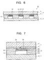
- a light emitting device 21 according to the second embodiment includes, as illustrated in Fig. 6 , a first light transmissive support 2 and a second light transmissive support 3 which are arranged to be opposed to each other with a predetermined gap provided therebetween. Between the first light transmissive support 2 and the second light transmissive support 3, a plurality of LED chips 22 are arranged.
- the LED chip 22 is configured such that a semiconductor layer is formed on an insulating substrate or a semiconductor substrate and a pair of electrodes are arranged on one surface.
- the LED chip 22 includes, as illustrated in Fig. 6 , a chip body (light emitting diode body) 27 having an N-type semiconductor layer (for example, an n-GaN layer) 24, an active layer (for example, an InGaN layer) 25, and a P-type semiconductor layer (for example, a p-GaN layer) 26 formed in order on an insulating substrate 23 such as a sapphire substrate.
- a chip body (light emitting diode body) 27 having an N-type semiconductor layer (for example, an n-GaN layer) 24, an active layer (for example, an InGaN layer) 25, and a P-type semiconductor layer (for example, a p-GaN layer) 26 formed in order on an insulating substrate 23 such as a sapphire substrate.
- the arrangement positions of the N-type semiconductor layer and the P-type semiconductor layer may be reversed.
- the double-sided electrode structure as in the LED chip 8 used in the first embodiment is not applicable.
- a single-sided electrode structure in which first and second electrodes 28, 29 are provided on the light emitting surface side of the chip body 27 is applied. Also to the LED chip 22 in which the semiconductor layer is formed on the semiconductor substrate, the single-sided electrode structure is sometimes applied.
- Each of the first and second electrodes 28, 29 of the LED chip 22 is electrically connected to a conductive circuit layer 5 of the first light transmissive support 2.
- the conductive circuit layer 5 and the first electrode 28 may be electrically connected with each other via a bump electrode 28B provided on the first electrode 28 as illustrated in Fig. 8 .
- the conductive circuit layer 5 and the second electrode 29 may be electrically connected with each other via a bump electrode 29B provided on the second electrode 29.
- the conductive circuit layer 5 is provided only on the surface of a first light transmissive insulator 4 constituting the first light transmissive support 2.
- the second light transmissive support 3 has no conductive circuit layer and is composed of only a second light transmissive insulator 6.
- a third light transmissive insulator 13 having the above-described Vicat softening temperature, tensile storage elastic modulus, glass transition temperature, and melting temperature is embedded as in the first embodiment.
- the constituent material of the third light transmissive insulator 13 is preferably a resin such as an elastomer or the like having the above-described Vicat softening temperature, tensile storage elastic modulus, glass transition temperature, and melting temperature in addition to the light transmitting property, the electric insulation property, the flexibility (flexibility) as in the first embodiment. Concrete examples and so on of the elastomer are as described above.
- the thickness of the third light transmissive insulator 13 is as in the above-described first embodiment.
- the resin in particular, the elastomer
- the resin having the above-described Vicat softening temperature, tensile storage elastic modulus, glass transition temperature, and melting temperature makes it possible to embed the third light transmissive insulator 13 in close contact with the plurality of LED chips 22, in the space between the first light transmissive support 2 and the second light transmissive support 3 while successfully maintaining the electrical connection between the conductive circuit layer 5 and the electrodes 28, 29 of the plurality of LED chips 22.
- the contact state between the conductive circuit layer 5 and the electrodes 28, 29 is maintained by the third light transmissive insulator 13 arranged in close contact with the peripheries of the LED chips 22.
- the electrical connection reliability between the conductive circuit layer 5 and the electrodes 28, 29 of the LED chips 22, in particular, the electrical connection reliability between the conductive circuit layer 5 and the electrodes 28, 29 when a bending test, a thermal cycle test (TCT) and so on are performed on the light emitting device 21, can be increased
- the resin having the above-described Vicat softening temperature, tensile storage elastic modulus, and melting temperature makes it possible to arrange the third light transmissive insulator 13 also at the peripheries of the first and second electrodes 28, 29.
- each of the first and second electrodes 28, 29 has an area smaller than that of the light emitting surface of the chip body 27 and a shape projecting from the light emitting surface, a space is generated between the surface (a non-forming surface of the first and second electrodes 28, 29) where the first and second electrodes 28, 29 are not formed within the light emitting surface and the conductive circuit layer 5 in the state that the first and second electrodes 28, 29 are in contact with the conductive circuit layer 5.
- the resin having the above-described Vicat softening temperature, tensile storage elastic modulus, and melting temperature makes it possible to successfully fill a part of the third light transmissive insulator 13 in the space between the non-forming surface of the first and second electrodes 28, 29 and the conductive circuit layer 5. This also applies to the case of forming the electrodes 28, 29 on the rear surface (the non-light emitting surface) of the chip body. Accordingly, it becomes possible to increase the electrical connection reliability between the conductive circuit layer 5 and the first and second electrodes 28, 29 of the LED chip 22 with higher reproducibility.
- the contact structure between the conductive circuit layer 5 and the first and second electrodes 28, 29 of the LED chip 22 it is also effective to apply the same structure as that in the first embodiment, namely, a structure in which the electrical connection regions where the conductive circuit layer 5 and the electrode 28, 29 is in direct contact with each other and the mechanical coupling regions where the part of the third light transmissive insulator 13 intervenes between the conductive circuit layer 5 and the electrode 28, 29, are formed on the contact interface between the conductive circuit layer 5 and the first or second electrode 28, 29.
- This can increase the mechanical coupling property while maintaining the electrical connection between the conductive circuit layer 5 and the electrode 28, 29. In other words, it becomes possible to increase the electrical connection reliability between the conductive circuit layer 5 and the first and second electrodes 28, 29 of the LED chip 22 with higher reproducibility.
- the first light transmissive support 2 having the first light transmissive insulator 4 and the conductive circuit layer 5 formed on the surface of the first light transmissive insulator 4, and the second light transmissive support 3 composed of only the second light transmissive insulator 6, are prepared.
- the constituent material and the forming method and so on of the conductive circuit layer 5 are as described above.
- a light transmissive insulating resin sheet 30 having a Vicat softening temperature in a range of 80 to 160°C is prepared.
- the light transmissive insulating resin sheet 30 preferably uses, as a main component, an elastomer that does not melt at the Vicat softening temperature at a tensile storage elastic modulus between 0°C and 100°C in a range of 0.1 to 10 GPa as described above, has a tensile storage elastic modulus at the Vicat softening temperature of 0.1 MPa or more, a melting temperature of 180°C or higher or higher by 40°C or more than the Vicat softening temperature, and a glass transition temperature of -20°C or lower.
- the light transmissive insulating resin sheet 30 is preferably an elastomer sheet having the above-described Vicat softening temperature, tensile storage elastic modulus, glass transition temperature, and melting temperature, and more preferably an acryl-based elastomer sheet.
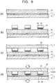
- the light transmissive insulating resin sheet 30 is disposed to cover the entire conductive circuit layer 5 ( Fig. 9(a) ).
- the light transmissive insulating resin sheet 30 has a shape capable of covering the entire conductive circuit layer 5 including portions that become arrangement positions of the LED chips 22 on the conductive circuit layer 5, and the entire light transmissive insulator 4.
- the plurality of LED chips 22 are arranged ( Fig. 9(b) ).
- the LED chips 22 are disposed such that the first and second electrodes 28, 29 are located on the light transmissive insulating resin sheet 30 side, in other words, located on the conductive circuit layer 5 side.
- the second light transmissive support 3 is disposed ( Fig. 9(c) ).
- the LED chips 22 are arranged between the first light transmissive insulating resin sheet 30 and the second light transmissive support 3 such that the first and second electrodes 28, 29 are located on the light transmissive insulating resin sheet 30 side.
- the light transmissive insulating resin sheet 30 only needs to have a thickness capable of sufficiently filling the space between the first light transmissive support 2 and the second light transmissive support 3, namely, the space based on the gap between the first light transmissive support 2 and the second light transmissive support 3 generated by arranging the LED chips 22 in the vacuum thermocompression bonding process illustrated below.
- the thickness of the light transmissive insulating resin sheet 30 only needs to be able to sufficiently fill the gap between the first light transmissive support 2 and the second light transmissive support 3 based on the height of the LED chip 22.
- a stack in which the first light transmissive support 2, the light transmissive insulating resin sheet 30, the LED chips 22, and the second light transmissive support 3 are stacked in order is pressurized while being heated in a vacuum atmosphere.
- a heating and pressurizing process (vacuum thermocompression bonding process) in the vacuum atmosphere for the stack is preferably performed under the same conditions as those in the first embodiment.
- the third light transmissive insulator 13 is formed which is in close contact with peripheries of the LED chips 22 while the first and second electrodes 28, 29 and the conductive circuit layer 5 are electrically connected with each other. Further, a part of the third light transmissive insulator 13 can be successfully filled in the space between the non-forming surface of the first and second electrodes 28, 29 within the light emitting surface of the chip body 27 and the conductive circuit layer 5. This makes it possible to obtain the light emitting device 21 improved in electrical connection between the conductive circuit layer 5 and the first and second electrodes 28, 29 of the LED chips 22 and its reliability with higher reproducibility.
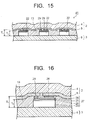
- FIG. 10 is a cross-sectional view illustrating a configuration of a light emitting device according to a third embodiment. Note that the same portions as those in the first and second embodiments are denoted by the same symbols and description thereof will be sometimes omitted.
- a light emitting device 31 illustrated in Fig. 10 includes a first light transmissive support 2 and a second light transmissive support 3 which are arranged to be opposed to each other with a predetermined gap provided therebetween.
- the first light transmissive support 2 includes a first light transmissive insulator 4 and a first conductive circuit layer 5 formed on the surface of the first light transmissive insulator 4.
- the second light transmissive support 3 includes a second light transmissive insulator 6 and a second conductive circuit layer 7 formed on the surface of the second light transmissive insulator 6.
- the first light transmissive support 2 and the second light transmissive support 3 are arranged with a predetermined gap provided therebetween so that the first conductive circuit layer 5 and the second conductive circuit layer 7 are opposed to each other.
- a plurality of light emitting diodes 8 are arranged in the gap between the first light transmissive support 2 and the second light transmissive support 3.
- the light transmissive insulators 4, 6, for example, a resin material having an insulation property, a light transmitting property, and flexibility is used.
- a resin material include polyethylene terephthalate (PET), polyethylene naphthalate (PEN), polycarbonate (PC), polyethylene succinate (PES), cyclic olefin resin (for example, ARTON (brand name) manufactured by JSR Corporation), acrylic resin and so on.
- the total light transmittances (JIS K7105) of the light transmissive insulators 4, 6 are preferably 90% or more, and more preferably 95% or more.
- the thicknesses of the light transmissive insulators 4, 6 are preferably in a range of 50 to 300 ⁇ m.
- the thicknesses of the light transmissive insulators 4, 6 are too large, there is a possibility that imparting excellent flexibility to the light transmissive supports 2, 3 becomes difficult and the light transmitting property also decreases. If the thicknesses of the light transmissive insulators 4, 6 are too small, characteristics and so on as the base material for forming the conductive circuit layers 5, 7 cannot be sufficiently obtained.
- the first conductive circuit layer 5 On the surface of the first light transmissive insulator 4, the first conductive circuit layer 5 is formed. Similarly, on the surface of the second light transmissive insulator 6, the second conductive circuit layer 7 is formed.
- a transparent conductive material such as indium tin oxide (ITO), fluorine-doped tin oxide (FTO), zinc oxide, indium zinc oxide (IZO) or the like is used.
- the conductive circuit layers 5, 7 made of the transparent conductive material include those made by applying the sputtering method, the electron beam evaporation method or the like to form a thin film and patterning the obtained thin film through laser beam machining, etching treatment or the like to form a circuit.
- the conductive circuit layers 5, 7 may be those made by applying a mixture of fine particles (for example, fine particles having an average particle size in a range of 10 to 100 nm) of the transparent conductive material and a transparent resin binder into a circuit shape by the screen printing or the like, or those made by performing patterning processing by the laser beam machining or photolithography to a coating film of the aforementioned mixture to form a circuit
- the conductive circuit layers 5, 7 are not limited to those made of the transparent conductive material but may be those made by forming fine particles of an opaque conductive material such as gold, silver or the like in a mesh form.
- the conductive circuit layers 5, 7 in the mesh form are formed by applying a photosensitive compound of the opaque conductive material such as silver halide and then performing exposure and developing treatments thereon.
- the conductive circuit layers 5, 7 may be formed by applying slurry containing opaque conductive material fine particles by the screen printing or the like in the mesh formed.
- the conductive circuit layers 5, 7 only need to be those that exhibit the light transmitting property when they are formed on the surfaces of the light transmissive insulators 4, 6 and provide the light transmissive supports 2, 3.
- the conductive circuit layers 5, 7 preferably have light transmitting properties so that the total light transmittances (JIS K7105) of the light transmissive supports 2, 3 are 10% or more and the total light transmittance as the whole light emitting device 31 is 1% or more. If the total light transmittance as the whole light emitting device 31 is less than 1%, the light emitting point is not recognized as a luminescent spot any longer.
- the light transmitting properties of the conductive circuit layers 5, 7 themselves differ depending on their configurations, but the total light transmittances are preferably in a range of 10 to 85%. If the total light transmittances of both of the conductive circuit layers 5, 7 exceed 85%, a wiring pattern becomes easily recognizable by the naked eyes, resulting in inconvenience as the light emitting device 31.
- the plurality of light emitting diodes 8 are arranged.
- a diode chip having a PN junction hereinafter, written as an LED chip 8
- the light emitting diode used herein is not limited to the LED chip 8 but may be a laser diode (LD) chip or the like.
- the plurality of LED chips 8 are arranged so that a minimum distance d being a minimum interval between the chips is 500 ⁇ m or more.
- the minimum distance d between the plurality of LED chips 8 is the distance from the outer peripheral surface of one LED chip 8 to the outer peripheral surface of the LED chip 8 located at the position closest thereto. Note that the minimum distance d between the LED chips 8 will be described later.
- the LED chip 8 for example, the one in which a P-type semiconductor layer is formed on an N-type semiconductor substrate, the one in which an N-type semiconductor layer is formed on a P-type semiconductor substrate, the one in which an N-type semiconductor layer and a P-type semiconductor layer are formed on a semiconductor substrate, the one in which a P-type hetero semiconductor layer and an N-type hetero semiconductor layer are formed on a P-type semiconductor substrate, the one in which an N-type hetero semiconductor layer and a P-type hetero semiconductor layer are formed on an N-type semiconductor substrate, and so on are known, and in any of them, electrodes 9, 10 are provided on both the upper and lower surfaces of the LED chips 8.
- the LED chip 8 used in the third embodiment includes as illustrated in Fig.
- the first electrode 9 is in direct contact with the first conductive circuit layer 5 and thereby electrically connected thereto. As described later, pressing the first conductive circuit layer 5 against the first electrode 9 electrically connects the first conductive circuit layer 5 and the first electrode 9.
- the second electrode 10 is in direct contact with the second conductive circuit layer 7 and thereby electrically connected thereto. Pressing the second conductive circuit layer 7 against the second electrode 10 electrically connects the second conductive circuit layer 7 and the second electrode 10.
- the conductive circuit layer 5 and the first electrode 9 may be electrically connected with each other via a bump electrode 9B provided on the first electrode 9 as illustrated in Fig. 12 .
- the LED chip 8 lights up by the DC voltage applied thereto via the first and second electrodes 9, 10.
- the first electrode 9 provided on the light emitting surface of the chip body 12 has an area smaller than that of the light emitting surface so as not to hinder light emission from the active layer 11 from being released to the outside.
- the light emitting surface of the chip body 12 has a forming surface and a non-forming surface of the first electrode 9. Further, the first electrode 9 has a shape projecting from the light emitting surface, for example, a shape projecting 0.1 ⁇ m or more.
- the second electrode 10 is provided on the entire non-light emitting surface of the chip body 12.
- the surface (a contact surface with the conductive circuit layer 7) of the second electrode 10 preferably has, for example, a projecting and recessed shape of 1 ⁇ m or more in order to increase the electrical connection reliability with the second conductive circuit layer 7, and more preferably has a shape with repeated fine projections and recesses.
- the surface (a contact surface with the conductive circuit layer 5) of the first electrode 9 also preferably has the same projecting and recessed shape. Note that on the surface of the electrode of an ordinary LED chip, a projecting and recessed shape is sometimes formed in addition to that for improving the electrical connection reliability.
- a third light transmissive insulator 13 is embedded.
- the third light transmissive insulator 13 preferably has a Vicat softening temperature in a range of 80 to 160°C.
- the tensile storage elastic modulus between 0°C and 100°C of the third light transmissive insulator 13 is preferably in a range of 0.01 to 10 GPa.
- the Vicat softening temperature of the third light transmissive insulator 13 is more preferably in a range of 100 to 140°C.
- the tensile storage elastic modulus between 0°C and 100°C of the third light transmissive insulator 13 is preferably in a range of 0.1 to 7 GPa.
- the third light transmissive insulator 13 does not melt at the Vicat softening temperature and has a tensile storage elastic modulus at the Vicat softening temperature of 0.1 MPa or more.
- the third light transmissive insulator 13 preferably has a melting temperature of 180°C or higher, or a melting temperature higher by 40°C or more than the Vicat softening temperature.
- the third light transmissive insulator 13 preferably has a glass transition temperature of -20°C or lower.
- the glass transition temperature of the third light transmissive insulator 13 is more preferably -40°C or lower. The measurement methods of those characteristics are as described above.
- the third light transmissive insulator 13 is preferably composed of a light transmissive insulating resin, in particular, an elastomer, satisfying characteristics such as the above-described Vicat softening temperature, tensile storage elastic modulus, melting temperature, glass transition temperature and so on.
- a light transmissive insulating resin in particular, an elastomer, satisfying characteristics such as the above-described Vicat softening temperature, tensile storage elastic modulus, melting temperature, glass transition temperature and so on.
- the elastomer an acryl-based elastomer, an olefin-based elastomer, a styrene-based elastomer, an ester-based elastomer, an urethane-based elastomer and so on are known.
- the acryl-based elastomer satisfying the above-described characteristics is excellent in flowability when softened, adhesiveness after curing, weather resistance and so on in addition to light transmitting property, electric insulation property, flexibility and so on, and is thus suitable as the constituent material of the third light transmissive insulator 13.
- the third light transmissive insulator 13 is preferably composed of the material containing the above-described elastomer as a main component, and may contain another resin component and so on as necessary
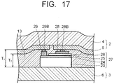
- the third light transmissive insulator 13 has a thickness smaller than a height T 1 (a height from the surface of the first electrode 9 to the surface of the second electrode 10) of the LED chip 8 in order to increase the contact property between the conductive circuit layers 5, 7 and the electrodes 9, 10. Note that in the case where a bump electrode 9A is provided on the first electrode 9, the height T 1 of the LED chip 8 is assumed to indicate the height from the top portion of the bump electrode 9A to the surface of the second electrode 10.
- the light transmissive support 2, 3 in close contact with the third light transmissive insulator 13 has a shape curved inward from a portion where the LED chip 8 is arranged toward intermediate portions with respect to the LED chips 8 adjacent thereto.
- the first and the second light transmissive supports 2, 3 have shapes curved inward from opposite directions respectively. Accordingly, the first light transmissive support 2 presses the first conductive circuit layer 5 against the first electrode 9 and the second light transmissive support 3 presses the second conductive circuit layer 7 against the second electrode 10. They can increase the electrical connection between the conductive circuit layers 5, 7 and the electrodes 9, 10 and its reliability.
- the third light transmissive insulator 13 has a minimum thickness T 2 smaller than the height T 1 of the LED chip 8 by a range of 5 ⁇ m or more and 1/2 T 1 or less, namely, a minimum thickness T 2 between the adjacent LED chips 8.
- the difference ⁇ T (T 1 - T 2 ) between the height T 1 of the LED chip 8 and the minimum thickness T 2 of the third light transmissive insulator 13 is in a range of 5 ⁇ m or more and 1/2 T 1 or less.
- the thickness difference ⁇ T is less than 5 ⁇ m, the force pressing the conductive circuit layers 5, 7 against the electrodes 9, 10 is insufficient, thus making the electrical connection state between the conductive circuit layers 5, 7 and the electrodes 9, 10, in particular, the electrical connection state in the bending resistance test and the thermal cycle test unstable. If the thickness difference ⁇ T exceeds 1/2 of the height T 1 (1/2 T 1 ) of the LED chip 8, maintenance of the shape of the third light transmissive insulator 13 may become difficult or the adhesiveness to the LED chip 8 or the like may decrease The thickness difference ⁇ T is more preferably in a range of 20 to 80 ⁇ m.
- the minimum thickness T 2 of the third light transmissive insulator 13 needs to be set in consideration of the minimum distance d between the LED chips 8 in addition to the height T 1 of the LED chip 8.
- the minimum distance d between the LED chips 8 is small, when the difference ⁇ T (T 1 - T 2 ) between the height T 1 of the LED chip 8 and the minimum thickness T 2 of the third light transmissive insulator 13 is made too small, the curved shapes of the conductive circuit layers 5, 7 become too sharp and may cause a defect.
- the corner on the light emitting surface side of the LED chip 8 bites into the first conductive circuit layer 5, and, for example, the N-type semiconductor layer and the P-type semiconductor layer of the LED chip 8 may short-circuit due to the first conductive circuit layer 5. This becomes a cause of occurrence of defective light emission of the LED chip 8.
- the minimum thickness T 2 of the third light transmissive insulator 13 is set based on the height T 1 of the LED chip 8 and the minimum distance d between the LED chips 8.
- the upper limit of the thickness difference ⁇ T is the straight line 4.
- the electrical connection reliability between the conductive circuit layers 5, 7 and the electrodes 9, 10 of the LED chip 8 and the reliability of the LED chip itself can be increased with high reproducibility.
- a light emitting device 31 can be provided which is excellent in light emitting reliability of each LED chip.
- the minimum distance d between the LED chips 8 is not particularly limited, the light emitting device 31 in the embodiment is effective when the plurality of LED chips 8 are densely mounted so that the minimum distance d between the LED chips 8 is 1500 ⁇ m or less.
- the conductive circuit layer is pressed against the electrodes of the LED chips for electrical connection, so that when a plurality of LED chips 8 are tried to be densely mounted, the electrical connection is likely to be unstable. Further, when the light emitting device is bent so that the radius of curvature becomes about 100 mm, the contact between the conductive circuit layers and the electrodes cannot be maintained any longer. Furthermore, there is a high possibility that the LED chips do not light up any longer at a thermal cycle of about 500 cycles.
- the above-described elastomer having a Vicat softening temperature in a range of 80 to 160°C makes it possible to embed the third light transmissive insulator 13 in close contact with the plurality of LED chips 8, in the space between the first light transmissive support 2 and the second light transmissive support 3.
- the contact state between the conductive circuit layers 5, 7 and the electrodes 9, 10 is maintained by the third light transmissive insulator 13 arranged in close contact with the peripheries of the LED chips 8. Accordingly, the electrical connection state between the conductive circuit layers 5, 7 and the electrodes 9, 10 can be further successfully maintained.
- the elastomer cannot be sufficiently softened in the formation process of the third light transmissive insulator 13, whereby the electrical connection between the conductive circuit layers 5, 7 and the electrodes 9, 10 may decrease.
- the Vicat softening temperature of the elastomer is below 80°C, the power for holding the LED chips 8 is insufficient, whereby the electrical connection reliability between the conductive circuit layers 5, 7 and the electrodes 9, 10 may decrease
- the third light transmissive insulator 13 also at the periphery of the first electrode 9.
- the first electrode 9 has the area smaller than that of the light emitting surface of the chip body 12 and the shape projecting from the light emitting surface, a space is generated between the surface (the non-forming surface of the first electrode 9) where the first electrode 9 is not formed within the light emitting surface and the first conductive circuit layer 5 in the state that the first electrode 9 is in contact with the conductive circuit layer 5.
- the third light transmissive insulator 13 is preferably filled also in a minute space between the non-forming surface of the first electrode 9 and the first conductive circuit layer 5.
- the filling state of the third light transmissive insulator 13 in the minute space can be improved by using the elastomer having a Vicat softening temperature in a range of 80 to 160°C.
- the third light transmissive insulator 13 exists in close contact with the periphery of the second electrode 10, so that the contact state is successfully maintained. Further, when the surface of the second electrode 10 has the projecting and recessed shape, the projections in the projecting and recessed shape can be brought into direct contact with the conductive circuit layer 7 to form electrical connection regions, and the third light transmissive insulator 13 can be filled in at least a part of the recesses in the projecting and recessed shape to form mechanical coupling regions.
- the electrical connection regions where the conductive circuit layer 7 and the electrode 10 are in direct contact with each other and the mechanical coupling regions where the third light transmissive insulator 13 intervenes between the conductive circuit layer 7 and the electrode 10, are formed on the contact interface between the conductive circuit layer 7 and the electrode 10.
- This can increase the mechanical coupling property while maintaining the electrical connection between the conductive circuit layer 7 and the electrode 10.
- the contact interface having the above-described electrical connection regions and mechanical coupling regions is effective not only to the contact portion between the second conductive circuit layer 7 and the second electrode 10 but also to the contact portion between the first conductive circuit layer 5 and the first electrode 9.
- the contact interface having the electrical connection regions and the mechanical coupling regions can be obtained not only when they have the projecting and recessed shapes but also when the electrodes 9, 10 have relatively flat surfaces, also by controlling the vacuum thermocompression bonding conditions and so on of the later-described transmissive insulating resin sheets.
- controlling the drawn state and the like of the resin sheets in the thermocompression bonding under vacuum of the light transmissive insulating resin sheets makes it possible to obtain the contact interfaces between the conductive circuit layers 5, 7 and the electrodes 9, 10 having the electrical connection regions and the mechanical coupling regions.
- first light transmissive support 2 having the first light transmissive insulator 4 and the first conductive circuit layer 5 formed on the surface of the first light transmissive insulator 4, and the second light transmissive support 3 having the second light transmissive insulator 6 and the second conductive circuit layer 7 formed on the surface of the second light transmissive insulator 6, are prepared.
- the constituent material and the forming method and so on of the conductive circuit layers 5, 7 are as described above.
- first and second light transmissive insulating resin sheets 14, 15 are prepared.
- the light transmissive insulating resin sheets 14, 15 are more preferably elastomer sheets having a Vicat softening temperature in a range of 80 to 160°C as described above, and furthermore preferably acryl-based elastomer sheets.
- the tensile storage elastic modulus of the elastomer sheet constituting the light transmissive insulating resin sheet 14, 15 between 0°C and 100°C is preferably in a range of 0.1 to 7 GPa. It is further preferable that the elastomer sheet does not melt at the Vicat softening temperature and has a tensile storage elastic modulus at the Vicat softening temperature of 0.1 MPa or more.
- the elastomer sheet preferably has a melting temperature of 180°C or higher, or a melting temperature higher by 40°C or more than the Vicat softening temperature.
- the glass transition temperature of the elastomer sheet is preferably -20°C or lower.
- the second light transmissive insulating resin sheet 15 is disposed to cover the entire conductive circuit layer 7 ( Fig. 14(a) ).
- the second light transmissive insulating resin sheet 15 has a shape capable of covering the entire conductive circuit layer 7 including portions that become arrangement positions of the LED chips 8 on the conductive circuit layer 7, and the entire light transmissive insulator 6.
- the plurality of LED chips 8 are arranged ( Fig. 14(b) ).
- the plurality of LED chips 8 are disposed such that the second electrodes 10 are located on the second light transmissive insulating resin sheet 15 side, in other words, located on the second conductive circuit layer 7 side and the minimum distance d is 500 ⁇ m or more. Further, on the plurality of LED chips 8, the first light transmissive insulating resin sheet 14 is disposed ( Fig. 14(c) ), and the first light transmissive support 2 is disposed thereon ( Fig. 14(d) ).
- the first light transmissive support 2 is disposed such that the first conductive circuit layer 5 faces the first light transmissive insulating resin sheet 14.
- the first light transmissive insulating resin sheet 14 has a shape capable of covering the entire conductive circuit layer 5 including portions that become the arrangement positions of the LED chips 8 on the conductive circuit layer 5, and further the entire light transmissive insulator 4. Accordingly, on the first light transmissive support 2 disposed on the first light transmissive insulating resin sheet 14, the entire first conductive circuit layer 5 is covered with the first light transmissive insulating resin sheet 15.
- the LED chips 8 are arranged between the first light transmissive insulating resin sheet 14 and the second light transmissive insulating resin sheet 15 such that the first electrodes 9 are located on the first light transmissive insulating resin sheet 14 side and the second electrodes 10 are located on the second light transmissive insulating resin sheet 15 side.
- the first and second light transmissive insulating resin sheets 14, 15 only need to have thicknesses capable of sufficiently filling the space between the first light transmissive support 2 and the second light transmissive support 3, namely, the space based on the gap between the first light transmissive support 2 and the second light transmissive support 3 generated by arranging the LED chips 8 in the vacuum thermocompression bonding process illustrated below.
- the total thickness of the first and second light transmissive insulating resin sheets 14, 15 only needs to be a thickness enough to form the third light transmissive insulator 13 having a shape based on the above-described difference ⁇ T (T 1 - T 2 ) between the height T 1 of the LED chip 8 and the minimum thickness T 2 of the third light transmissive insulator 13.
- a stack in which the second light transmissive support 3, the second light transmissive insulating resin sheet 15, the LED chips 8, the first light transmissive insulating resin sheet 14, and the first light transmissive support 2 are stacked in order is pressurized while being heated in a vacuum atmosphere.
- a pressurizing process for the stack is preferably performed using a pressure device capable of locally applying a pressure between adjacent LED chips 8, for example, a pressure device having a pressure plate provided with an elastic body such as rubber on the surface so that the minimum thickness T 2 of the third light transmissive insulator 13 is smaller than the height T 1 of the LED chip 8.
- a heating and pressurizing process (vacuum thermocompression bonding process) in the vacuum atmosphere for the stack is preferably performed by pressurizing the stack while heating it to a temperature T in a range of Mp - 10 (°C) ⁇ T ⁇ Mp + 30 (°C) with respect to a Vicat softening temperature Mp (°C) of the light transmissive insulating resin sheets 14, 15. Applying such heating conditions makes it possible to pressurize the stack in a state that the light transmissive insulating resin sheets 14, 15 are moderately softened.
- the heating temperature T in the thermocompression bonding of the stack is below a temperature lower than by 10 (°C) than the Vicat softening temperature Mp of the light transmissive insulating resin sheets 14, 15 (T ⁇ Mp - 10), there is a possibility that the softening of the light transmissive insulating resin sheets 14, 15 becomes insufficient, so that the adhesiveness of the light transmissive insulating resin sheets 14, 15 (accordingly, the third light transmissive insulator 13) to the LED chip 8 decreases.
- the light transmissive insulating resin sheets 14, 15 (accordingly, the third light transmissive insulator 13) cannot be successfully filled in the space between the non-forming surface of the first electrode 9 within the light emitting surface of the chip body 12 and the first conductive circuit layer 5. If the heating temperature T exceeds a temperature higher by 30 (°C) than the Vicat softening temperature Mp of the light transmissive insulating resin sheets 14, 15 (Mp + 30 ⁇ T), there is a possibility that the light transmissive insulating resin sheets 14, 15 are softened too much to cause a defective shape or the like.
- thermocompression bonding process in the vacuum atmosphere for the stack is preferably performed as follows. Preliminarily pressurization is performed on the above-described stack to bring its components into close contact with one another. Then, a working space in which the preliminarily pressurized stack is placed is evacuated, and then pressurization is performed on the stack while heating it to the above-described temperature. Thermocompression bonding the preliminarily pressurized stack in the vacuum atmosphere as described above makes it possible to embed the softened light transmissive insulating resin sheets 14, 15 in the space between the first light transmissive support 2 and the second light transmissive support 3 without any gap therebetween.
- the vacuum atmosphere in the thermocompression bonding is preferably 5 Pa or less.
- the preliminarily pressurization process can be omitted, but in this case, positional displacement or the like becomes likely to occur in the stack, and therefore it is preferable to perform the preliminarily pressurization process.
- thermocompression bonding process for the stack is performed under the air atmosphere or a low vacuum
- bubbles are likely to remain in the light emitting device 31 after the thermocompression bonding, in particular, around the LED chips 8.
- the bubbles remaining in the light emitting device 31 are pressurized and therefore become a cause of swelling of the light emitting device 31 after the thermocompression bonding or peeling of the LED chips 8 from the light transmissive supports 2, 3.
- the bubbles or swelling exists inside the light emitting device 31, in particular, near the LED chips 8, light is non-uniformly scattered, unfavorably leading to a problem in external appearance of the light emitting device 31.
- the occurrence of the bubbles in the light emitting device 31 can be suppressed based on the various characteristics of the third light transmissive insulator 13, the vacuum thermocompression bonding conditions or the like. It is preferable that bubbles having an outer diameter of 500 ⁇ m or more or a size of equal to or larger than an external shape size of the LED chip 8 do not exist in the light emitting device 31 of the embodiment
- the hot melt adhesive described in the aforementioned Patent Reference 2 melts when heated, it is difficult to perform the bonding process (thermocompression bonding process) under vacuum. Therefore, in the light emitting device produced by thermocompression bonding the stack with the hot melt adhesive sheet intervening, bubbles due to remaining air are likely to remain, and many bubbles are likely to remain, in particular, near the LED chips.
- the remaining bubbles are formed by pressurization, and swelling of the bubbles occurs with time because the inner pressure is, for example, 0.1 MPa or more. Therefore, the light emitting device having the remaining bubbles, even if lighting up immediately after being produced, loses the electrical connection due to the swelling of the bubbles occurring with time, resulting in non-lighting in many products.
- the light emitting device 31 and a method for manufacturing the same in the embodiment have been improved in the drawbacks in the manufacturing process of the conventional device.
- the pressurizing force to be applied in the thermocompression bonding of the stack differs depending on the heating temperature, the material and thicknesses of the light transmissive insulating resin sheets 14, 15, the final thickness of the third light transmissive insulator 13 and so on, but is usually preferably in a range of 0.5 to 20 MPa, and more preferably in a range of 1 to 12 MPa
- Applying the pressurizing force makes it possible to increase the embedding property of the softened light transmissive insulating resin sheets 14, 15 in the gap between the first light transmissive support 2 and the second light transmissive support 3. Further, it is possible to suppress the decrease in characteristics, breakage and so on of the LED chips 8.
- the thickness of the third light transmissive insulator 13 can be controlled in a desired range while the first electrodes 9 and the first conductive circuit layer 5 are electrically connected with each other and the second electrodes 10 and the second conductive circuit layer 7 are electrically connected with each other. Further, it is possible to bring the third light transmissive insulator 13 into close contact with the peripheries of the LED chips 8 including the peripheries of the first electrodes 9. This makes it possible to obtain the light emitting device 31 improved in electrical connection reliability between the conductive circuit layers 5, 7 and the electrodes 9, 10.
- controlling the heating temperature or the pressurizing force in the vacuum thermocompression bonding of the stack, or the shape, the hardness or the like of a pressurizing body makes it possible to form the electrical connection regions where the electrode 9, 10 and the conductive circuit layer 5, 7 are in direct contact with each other and the mechanical coupling regions where the electrode 9, 10 and the conductive circuit layer 5, 7 are coupled with each other with the third light transmissive insulator 13 intervening therebetween, on the contact interface between the first electrode 9 or the second electrode 10 and the conductive circuit layer 5, 7 (in particular, the contact interface between the second electrode 10 and the conductive circuit layer 7).
- the electrical connection reliability can be further increased
- a light emitting device 41 according to the fourth embodiment includes, as illustrated in Fig. 15 , a first light transmissive support 2 and a second light transmissive support 3 which are arranged to be opposed to each other with a predetermined gap provided therebetween.
- a plurality of LED chips 22 are arranged in the gap between the first light transmissive support 2 and the second light transmissive support 3.
- the LED chip 22 is configured such that a semiconductor layer is formed on an insulating substrate or a semiconductor substrate and a pair of electrodes are arranged on one surface (the upper surface in Fig. 15 ).
- the LED chip 22 includes, as illustrated in Fig. 16 , a chip body (light emitting diode body) 27 having an N-type semiconductor layer (for example, an n-GaN layer) 24, an active layer (for example, an InGaN layer) 25, and a P-type semiconductor layer (for example, a p-GaN layer) 26 formed in order on an insulating substrate 23 such as a sapphire substrate.
- a chip body (light emitting diode body) 27 having an N-type semiconductor layer (for example, an n-GaN layer) 24, an active layer (for example, an InGaN layer) 25, and a P-type semiconductor layer (for example, a p-GaN layer) 26 formed in order on an insulating substrate 23 such as a sapphire substrate.
- the arrangement positions of the N-type semiconductor layer and the P-type semiconductor layer may be reversed.
- a double-sided electrode structure as in the LED chip 8 used in the third embodiment is not applicable.
- first and second electrodes 28, 29 are provided on one surface side of the chip body 27 . Also to the LED chip 22 in which the semiconductor layer is formed on the semiconductor substrate, the single-sided electrode structure is sometimes applied.
- Each of the first and second electrodes 28, 29 of the LED chip 22 is electrically connected to a first conductive circuit layer 5 of the first light transmissive support 2.
- the first conductive circuit layer 5 and the first electrode 28 may be electrically connected with each other via a bump electrode 28B provided on the first electrode 28 as illustrated in Fig. 17 .
- the conductive circuit layer 5 and the second electrode 29 may be electrically connected with each other via a bump electrode 29B provided on the second electrode 29.
- the first conductive circuit layer 5 is provided only on the surface of a first light transmissive insulator 4 constituting the first light transmissive support 2.
- the second light transmissive support 3 has no conductive circuit layer and is composed of only a second light transmissive insulator 6.
- a third light transmissive insulator 13 is embedded as in the third embodiment.
- the constituent material of the third light transmissive insulator 13 preferably has the same characteristics such as the Vicat softening temperature, tensile storage elastic modulus, melting temperature, and glass transition temperature as those in the third embodiment, and the light transmitting property, the electric insulation property, the flexibility (bendability), and is more preferably an elastomer. Concrete examples and so on of the elastomer are as described above.
- the third light transmissive insulator 13 has a thickness smaller than a height T 1 of the LED chip 22 as in the third embodiment in order to increase the contact property between the conductive circuit layer 5 and the first and second electrodes 28, 29.
- the first light transmissive support 2 in close contact with the third light transmissive insulator 13 has a shape curved inward from a portion where the LED chip 22 is arranged toward intermediate portions with respect to the LED chips 8 adjacent thereto. Accordingly, the first light transmissive support 2 presses the first conductive circuit layer 5 against the first and second electrodes 28, 29. This can increase the electrical connection between the conductive circuit layer 5 and the first and second electrodes 28, 29 and its reliability.
- the third light transmissive insulator 13 has a minimum thickness T 2 smaller than the height T 1 of the LED chip 22 by a range of 5 ⁇ m or more and 1/2 T 1 or less.
- the difference ⁇ T (T 1 - T 2 ) between the height T 1 of the LED chip 22 and the minimum thickness T 2 of the third light transmissive insulator 13 is in a range of 5 ⁇ m or more and 1/2 T 1 or less.
- the reason for defining the minimum thickness T 2 of the third light transmissive insulator 13 and the thickness difference ⁇ T is the same as that in the third embodiment.
- the electrical connection reliability between the conductive circuit layer 5 and the first and second electrodes 28, 29 of the LED chip 22 and the reliability of the LED chip 22 itself can be increased with high reproducibility.
- a light emitting device 41 can be provided which is excellent in light emitting reliability of each LED chip.
- the minimum distance d between the LED chips 8 is not particularly limited, the light emitting device 41 in the embodiment is effective when a plurality of LED chips 8 are densely mounted so that the minimum distance d between the LED chips 8 is 1500 ⁇ m or less.
- the first light transmissive insulator 4 is preferably formed of an insulating resin body (sheet or the like) having the light transmitting property and the flexibility in order to inwardly curve the first light transmissive support 2.
- the second light transmissive insulator 6 is not limited to the insulating resin body but may be made of, for example, an inorganic material having both the insulation property and the light transmitting property such as, for example, glass. In the case of using a glass substrate as the light transmissive insulator 6, it is impossible to impart the flexibility to the whole light emitting device 41. In the case of imparting the flexibility to the light emitting device 41, it is preferable to form not only the first light transmissive insulator 4 but also the second light transmissive insulator 6 using insulating resin bodies having the light transmitting property and the flexibility.
- the third light transmissive insulator 13 also at the peripheries of the first and second electrodes 28, 29 as in the third embodiment.
- each of the first and second electrodes 28, 29 has an area smaller than that of an electrode forming surface (for example, the light emitting surface) of the chip body 27 and a shape projecting from the electrode forming surface, a space is generated between the surface (a non-forming surface of the first and second electrodes 28, 29) where the first and second electrodes 28, 29 are not formed within the electrode forming surface and the conductive circuit layer 5 in the state that the first and second electrodes 28, 29 are in contact with the conductive circuit layer 5. It is preferable to fill the third light transmissive insulator 13 also in the minute space between the non-forming surface of the first and second electrodes 28, 29 and the conductive circuit layer 5.
- the contact structure between the conductive circuit layer 5 and the first and second electrodes 28, 29 of the LED chip 22 it is effective to apply the same structure as that in the third embodiment, namely, the structure in which the electrical connection regions where the conductive circuit layer 5 and the electrode 28, 29 are in direct contact with each other and the mechanical coupling regions where the third light transmissive insulator 13 intervenes between the conductive circuit layer 5 and the electrode 28, 29, are formed on the contact interface between the conductive circuit layer 5 and the first or second electrode 28 or 29.
- This can increase the mechanical coupling property while maintaining the electrical connection between the conductive circuit layer 5 and the electrode 28, 29. In other words, it becomes possible to increase the electrical connection reliability between the conductive circuit layer 5 and the first and second electrodes 28, 29 of the LED chip 22 with higher reproducibility.
- the first light transmissive support 2 having the first light transmissive insulator 4 and the first conductive circuit layer 5 formed on the surface of the first light transmissive insulator 4, and the second light transmissive support 3 composed of only the second light transmissive insulator 6, are prepared.
- the constituent material and the forming method and so on of the conductive circuit layer 5 are as described above.
- a light transmissive insulating resin sheet 30 is prepared.
- the light transmissive insulating resin sheet 30 is preferably the same elastomer sheet as that in the third embodiment, and more preferably an acryl-based elastomer sheet. The characteristics of the elastomer sheet are as described above.
- the light transmissive insulating resin sheet 30 is disposed to cover the entire conductive circuit layer 5 ( Fig. 18(a) ).
- the light transmissive insulating resin sheet 30 has a shape capable of covering the entire conductive circuit layer 5 including portions that become arrangement positions of the LED chips 22 on the conductive circuit layer 5, and the entire first light transmissive support 2.
- the plurality of LED chips 22 are arranged ( Fig. 18(b) ). The LED chips 22 are disposed such that the first and second electrodes 28, 29 are located on the light transmissive insulating resin sheet 30 side, in other words, located on the conductive circuit layer 5 side.
- the second light transmissive support 3 is disposed on the LED chips 22 so that the minimum distance d is 500 ⁇ m or more ( Fig. 18(c) ).
- the LED chips 22 are arranged between the light transmissive insulating resin sheet 30 and the second light transmissive support 3.
- the light transmissive insulating resin sheet 30 only needs to have a thickness capable of sufficiently filling the space between the first light transmissive support 2 and the second light transmissive support 3, namely, the space based on the gap between the first light transmissive support 2 and the second light transmissive support 3 generated by arranging the LED chips 22 in the vacuum thermocompression bonding process.
- the thickness of the light transmissive insulating resin sheet 30 only needs to be a thickness enough to form the third light transmissive insulator 13 having a shape based on the above-described difference ⁇ T (T 1 - T 2 ) between the height T 1 of the LED chip 22 and the minimum thickness T 2 of the third light transmissive insulator 13.
- a stack in which the first light transmissive support 2, the light transmissive insulating resin sheet 30, the LED chips 22, and the second light transmissive support 3 are stacked in order is pressurized while being heated in a vacuum atmosphere.
- a heating and pressurizing process (vacuum thermocompression bonding process) in the vacuum atmosphere for the stack is preferably performed under the same conditions as those in the third embodiment.
- the thickness of the third light transmissive insulator 13 can be controlled into a desired range while the first and second electrodes 28, 29 and the conductive circuit layer 5 are electrically connected with each other. Further, it is possible to bring the third light transmissive insulator 13 into close contact with the peripheries of the LED chips 22 including the peripheries of the electrodes 28, 29. This makes it possible to obtain the light emitting device 41 improved in electrical connection reliability between the conductive circuit layer 5 and the first and second electrodes 28, 29.
- a light emitting device composed of three light transmissive insulators in total with the first light transmissive support 2 formed using two light transmissive insulators 4 even a light emitting device in which the numbers of light transmissive insulators of the light transmissive supports 2, 3 are variously changed, and the like, can provide the same effects as those of the first to fourth embodiments.
- the light emitting devices 1, 21, 31, 41 in the first to fourth embodiments use the light transmissive members for the supports 2, 3 that hold the LED chips 8, 22 therebetween, and therefore suitable for display devices that display various character strings, geometrical figures and patterns and the like on a door or a window of a building such as a shop, a showroom, an office or the like, display devices such as a display plate, a bulletin board and the like, vehicular lamps such as a brake lamp, a blinker lamp and the like.
- Fig. 19 illustrates a door 51 of a building to which the light emitting device 1 (21, 31, 41) in the embodiment is attached, as a usage example of the light emitting devices 1, 21, 31, 41 in the embodiments.
- the light emitting device 1 (21, 31, 41) includes a glass plate 53 installed in a door frame 52, and the light emitting device 1 (21, 31, 41) attached to the glass plate 53.
- the light emitting device 1 (21,31,41) has the light transmitting property as a whole, and therefore enables, for example, display as the door (ENTRANCE in Fig. 19 ) and never loses transparency of the glass plate 53 constituting the door 51.
- the light emitting devices 1, 21, 31, 41 in the embodiments are suitably used for various display devices and lamps required to have transparency.
- polyethylene terephthalate sheets having a thickness of 180 ⁇ m were prepared as first and second light transmissive insulators.
- first and second light transmissive insulators On the surface of the polyethylene terephthalate sheet as the first light transmissive insulator, slurry made by dispersing ITO fine particles in an ultraviolet cure acryl-based transparent resin binder was printed to form a conductive circuit layer in which six linearly arranged LED chips were connected in series, thereby producing a first light transmissive support.
- a conductive circuit layer was similarly formed to produce a second light transmissive support.
- first and second light transmissive insulating resin sheets acryl-based elastomer sheets having a Vicat softening temperature of 110°C, a melting temperature of 220°C, a glass transition temperature of -40°C, a tensile storage elastic modulus at 0°C of 1.1 GPa, a tensile storage elastic modulus at 100°C of 0.3 GPa, a tensile storage elastic modulus at 110°C being a Vicat softening point of 0.2 GPa, and a thickness of 60 ⁇ m were prepared.
- the Vicat softening temperature was obtained using a heat distortion tester No. 148-HD-PC manufactured by Yasuda Seiki Seisakusho, Ltd. under the conditions of a test load of 10 N and a rate of heating of 50 °C/hour and under A50 condition described in JIS K7206 (ISO 306).
- the glass transition temperature and the melting temperature were obtained by the method complying with JIS K7121 (ISO 3146), using a differential scanning calorimeter DSC-60 manufactured by Shimadzu Corporation, at a rate of heating of 5 °C/min, by heat flux differential scanning calorimetry.
- the tensile storage elastic modulus was obtained complying with JIS K7244-4 (ISO 6721-4), using a dynamic viscoelasticity automatic measuring device DDV-01GP manufactured by A&D Company, Limited, at a rate of uniform heating of 1 °C/min from -100°C to 200°C, and at a frequency of 10 Hz.
- the characteristic values of elastomers in the following working examples and comparative examples were measured by the same method and conditions as those in Example 1.
- the prepared LED chip includes a first electrode provided on the light emitting surface side of the chip body and a second electrode provided on the non-light emitting surface of the chip body, and has a height of 175 ⁇ m.
- the first electrode has an area smaller than that of the light emitting surface of the chip body and has a shape projecting from the light emitting surface.
- a projecting amount of the first electrode from the light emitting surface is 3 ⁇ m.
- An area ratio of the forming surface of the first electrode to the light emitting surface of the chip body is about 20%.
- About 80% (area ratio) of the light emitting surface of the chip body is the non-forming surface of the electrode.
- the second electrode is formed on the entire non-light emitting surface of the chip body and its surface is provided with fine projections and recesses.
- the second light transmissive insulating resin sheet was placed to cover the entire conductive circuit layer and light transmissive insulator, and the six LED chips were arranged at predetermined positions on the second light transmissive insulating resin sheet.
- the six LED chips were arranged such that their second electrodes were located on the second light transmissive insulating resin sheet side.
- the first light transmissive insulating resin sheet and the first light transmissive support were stacked.
- the first light transmissive insulating resin sheet was arranged such that the conductive circuit layer of the first light transmissive support was located on the first light transmissive insulating resin sheet side.
- the first light transmissive insulating resin sheet has a shape covering the entire conductive circuit layer and light transmissive insulator of the first light transmissive support.
- a stack in which the second light transmissive support, the second light transmissive insulating resin sheet, the LED chips, the first light transmissive insulating resin sheet, and the first light transmissive support were stacked in order was preliminarily pressed with a pressure of 0.1 MPa, and then a working space was evacuated to 0.1 kPa.
- the stack was pressed with a pressure of 9.8 MPa while being heated to 120°C in a vacuum atmosphere of 5 kPa.
- This heating and pressurizing state was kept for 10 minutes to embed the first and second light transmissive insulating resin sheets between the first light transmissive support and the second light transmissive support to thereby form a third light transmissive insulator, while electrically connecting the electrodes of the LED chips and the conductive circuit layers. Thereafter, sealing processing using an ultraviolet cure resin was performed on an end face, thereby producing a light emitting device. The obtained light emitting device was subjected to later-described characteristic evaluation.
- bubbles and a status of swelling caused thereby were visually confirmed with the naked eyes after it was left to stand for 24 hours from production. As a result, visible bubbles and swelling seemed to be caused thereby were not observed.
- the evaluation of bubbles was carried out as follows. The front surface or the rear surface of the light emitting device was visually observed, and the presence or absence of bubbles was primarily confirmed. Samples in which bubbles were not observed in the primary confirmation were determined to have no bubbles, and the inspection was finished. Samples in which bubbles were observed in the primary inspection were subjected to photographing of the bubbles using a microscope with camera.
- a distance between arbitrary two points on a contour of the bubble was measured, and a length having a maximum distance was defined as an outer diameter. Then, the case where the outer diameter of the bubble was an LED chip size or more, or 500 ⁇ m or more was determined to have bubbles, and samples other than those were determined to have no bubbles.
- the LED chip and its surroundings were observed under SEM.
- a part of the third light transmissive insulator was successfully filled between the non-forming surface of the first electrode within the light emitting surface of the LED chip and the conductive circuit layer.
- the electrical connection regions where the second electrode and the conductive circuit layer were in direct contact with each other and the mechanical coupling regions where a part of the third light transmissive insulator intervened between the second electrode and the conductive circuit layer, were formed on the contact interface between the second electrode and the conductive circuit layer.
- the same observation results with the naked eyes and SEM were obtained also in Examples 2, 18.
- Light emitting devices were produced as in Example 1 except that an acryl-based elastomer sheet having the Vicat softening temperature, tensile storage elastic modulus, glass transition temperature, and melting temperature listed in Table 2 and Table 3 was used as the light transmissive insulating resin sheet, and that the heating temperature listed in Table 3 was applied in pressunzation. These light emitting devices were subjected to later-described characteristic evaluation.
- Light emitting devices were produced as in Example 1 except that the conductive circuit layer was formed of an ITO sputtered film, and an acryl-based elastomer sheet having the Vicat softening temperature, tensile storage elastic modulus, glass transition temperature, and melting temperature listed in Table 2 and Table 3 was used as the light transmissive insulating resin sheet, and that the heating temperature listed in Table 3 was applied in pressunzation. These light emitting devices were subjected to characteristic evaluation.
- Polyethylene terephthalate sheets having a thickness of 180 ⁇ m were prepared as first and second light transmissive insulators.
- a conductive circuit layer in which six linearly arranged LED chips were connected in series was formed as in Working Example 1, thereby producing a first light transmissive support
- the polyethylene terephthalate sheet as the second light transmissive insulator was used as it was as the second light transmissive support
- As the light transmissive insulating resin sheet an acryl-based elastomer sheet having a Vicat softening temperature of 110°C, a glass transition temperature of -40°C, a melting temperature of 220°C, a tensile storage elastic modulus at 0°C of 1.1 GPa, a tensile storage elastic modulus at 100°C of 0.3 GPa, a tensile storage elastic modulus at 110°C being a Vicat softening point of 0.3 GPa,
- the prepared LED chip includes first and second electrodes provided on the light emitting surface side of the chip body, and has a height of 90 ⁇ m.
- Each of the first and second electrodes has an area smaller than that of the light emitting surface of the chip body and has a shape projecting from the light emitting surface.
- a projecting amount of the electrode from the light emitting surface is 1 ⁇ m.
- An area ratio of the forming surface of the first and second electrodes to the light emitting surface of the chip body is about 15%.
- About 85% (area ratio) of the light emitting surface of the chip body is the non-forming surface of the electrodes.
- the light transmissive insulating resin sheet was placed to cover the entire conductive circuit layer, and the six LED chips were arranged at predetermined positions on the light transmissive insulating resin sheet.
- the six LED chips were arranged such that their first and second electrodes were located on the light transmissive insulating resin sheet side.
- the second light transmissive support was stacked. Then, the stack in which the first light transmissive support, the light transmissive insulating resin sheet, the LED chips, and the second light transmissive support were stacked in order was subjected to heating and pressurization processing under vacuum under the same conditions as those in Working Example 1. Sealing processing using an ultraviolet cure resin was performed on an end face, thereby producing a light emitting device. The obtained light emitting device was subjected to later-described characteristic evaluation
- a light emitting device was produced as in Example 11 except that the conductive circuit layer was formed of an ITO sputtered film. The obtained light emitting device was subjected to later-described characteristic evaluation.
- Polyethylene terephthalate sheets having a thickness of 180 ⁇ m were prepared as first and second light transmissive insulators
- slurry made by dispersing Ag fine particles in an acryl-based transparent resin binder was printed into a mesh shape with an opening of 0.5 mm to form a conductive circuit layer in which six linearly arranged LED chips were connected in series, thereby producing a first light transmissive support
- a conductive circuit layer was similarly formed to produce a second light transmissive support.
- a light emitting device was produced as in Example 1 except that the first and second light transmissive supports were used The obtained light emitting device was subjected to later-described characteristic evaluation.
- Light emitting devices were produced as in Example 13 except that an acryl-based elastomer sheet having the Vicat softening temperature, tensile storage elastic modulus, glass transition temperature, and melting temperature listed in Table 2 and Table 3 was used as the light transmissive insulating resin sheet, and that the heating temperature listed in Table 3 was applied in pressurization.
- the light emitting devices were subjected to later-described characteristic evaluation.
- a light emitting device was produced as in Example 11 except that the same conductive circuit layer in the mesh form as that in Example 13 was used The obtained light emitting device was subjected to later-described characteristic evaluation.
- Light emitting devices were produced as in Example 1 except that an acryl-based elastomer sheet having the Vicat softening temperature, tensile storage elastic modulus, glass transition temperature, and melting temperature listed in Table 2 and Table 3 was used as the light transmissive insulating resin sheet, and that the heating temperature listed in Table 3 was applied in pressurization. These light emitting devices were subjected to later-described characteristic evaluation.
- First and second light transmissive supports were produced as in Example 1.
- Acryl-based highly viscous adhesive sheets having a thickness of 100 ⁇ m were prepared, and through holes slightly larger than the LED chips were formed therein so that six LED chips were linearly arranged.
- the acryl-based highly viscous adhesive sheet having the through holes was placed on the second light transmissive support, and then the same LED chips as those in Examples 1 were arranged in the through holes.
- the first light transmissive support was stacked, and then the resultant was sandwiched between thermal drums and thereby pressed with a pressure of 9.8 MPa while being heated to 160°C. Thereafter, sealing processing was performed on an end face, whereby a light emitting device was produced.
- the obtained light emitting device was subjected to later-described characteristic evaluation.
- First and second light transmissive supports were produced as in Example 11. At predetermined positions on the second light transmissive support, the same six blue light emitting GaN-based LED chips as those in Example 11 were arranged. The surfaces of the LED chips on the sapphire substrate side were fixed to the second light transmissive support with an adhesive. The first light transmissive support was stacked on the LED chips, and then an acrylic pressure sensitive adhesive was filled under a vacuum atmosphere in the gap between the first light transmissive support and the second light transmissive support The acrylic pressure sensitive adhesive was irradiated with an ultraviolet ray and thereby partially cured, whereby a light emitting device was produced. The obtained light emitting device was subjected to later-described characteristic evaluation.
- a polyethylene terephthalate sheet having a thickness of 180 ⁇ m becoming a first light transmissive insulator On the surface of a polyethylene terephthalate sheet having a thickness of 180 ⁇ m becoming a first light transmissive insulator, slurry made by dispersing ITO fine particles was printed to form a first conductive circuit layer. Then, on a polyethylene terephthalate sheet having a thickness of 180 ⁇ m becoming a second light transmissive insulator, an acryl-based elastomer sheet having a Vicat softening temperature of 110°C, a glass transition temperature of - 10°C, a melting temperature of 220°C, a tensile storage elastic modulus at 0°C of 0.006 GPa, a tensile storage elastic modulus at 100°C of 0.003 GPa, a tensile storage elastic modulus at 110°C being a Vicat softening point of 0.2 GPa, and a thickness of 60 ⁇
- Blue light emitting GaN-based LED chips were arranged with their sapphire substrate side located at the predetermined positions on the acryl-based elastomer sheet.
- the first light transmissive support was stacked on the LED chips so that the first conductive circuit layer was located on the electrode side of the LED chips.
- the stack was pressed with a pressure of 9.8 MPa while being heated to 160°C in a vacuum atmosphere.
- the heating and pressurizing state was kept for one hour, whereby a light emitting device was produced.
- the obtained light emitting device was subjected to later-described characteristic evaluation.
- a light emitting device was produced as in Example 1 except that an acryl-based elastomer sheet having a Vicat softening temperature of 110°C, a glass transition temperature of -40°C, a melting temperature of 220°C, a tensile storage elastic modulus at 0°C of 0.006 GPa, a tensile storage elastic modulus at 100°C of 0.003 GPa, a tensile storage elastic modulus at 110°C being a Vicat softening point of 0.002 GPa, and a thickness of 60 ⁇ m, and that thermocompression bonding was carried out in the atmosphere.
- the obtained light emitting device was subjected to later-described characteristic evaluation.
- a light emitting device was produced as in Example 1 except that an olefin-based hot melt adhesive sheet having a softening point by the ring and ball method of 145°C and a thickness of 60 ⁇ m was used in place of the acryl-based elastomer sheet, and that the stack was hot-roll pressed under the conditions of 160°C for 20 seconds in the atmosphere. This light emitting device was subjected to later-described characteristic evaluation.
- a light emitting device was produced as in Comparative Example 11 except that an olefin-based hot melt adhesive sheet having a thickness of 87.5 ⁇ m was used. This light emitting device was subjected to later-described characteristic evaluation.
- Examples 1 to 18 and Comparative Examples 1 to 12 were evaluated as follows. Twelve samples were produced for each of Examples 1 to 18 and Comparative Examples 1 to 12. For the 12 samples of each of the examples, the bending resistance test described in JIS C5016 (IEC249-1 and IEC326-2) 8.6 was carried out in an energization state. The bending test was carried out for all of the samples under the circumstances of a temperature of 20 ⁇ 2°C, a relative humidity of 60 to 70%, and a pressure of 86 to 106 kPa.
- the minimum bending radius (the minimum value of the bending radius with which lighting was maintained) of the sample bent in the direction perpendicular to the arrangement direction of the LED chips was investigated.
- a plurality of kinds of circular cylinders for measurement having a uniform diameter with a radius of 100 mm to 5 mm and having a cross section in a true-circle shape were prepared. Then, the obtained light emitting device was set such that the rear surface of the light emitting surface of the LED chip was in contact with the curved surface on the surface of the circular cylinder for measurement. The light emitting device was made to light up and bent in this state at 180° along the curved surface on the surface of the circular cylinder for measurement. This bending test was carried out in order from a circular cylinder for measurement with a large radius to a circular cylinder for measurement with a small radius, and to which bending radius of the circular cylinder for measurement the lighting state was maintained, was measured.
- the thermal cycle test was carried out according to JIS C60068-14 between -20°C and 60°C to investigate the number of cycles with which the lighting state was able to be maintained.
- the thermal cycle test was carried out under the conditions of an exposure time of 30 minutes and a rate of heating of 3 K/min.
- each of the light emitting devices according to Examples 1 to 18 maintained lighting even in a state where the bending radius was made small in the bending resistance test, and was able to maintain the lighting state up to a sufficient number of cycles in the thermal cycle test. Accordingly, it is understood that each of the light emitting devices according to Examples 1 to 18 is excellent in bending resistance and thermal cycle resistance characteristics. In other words, it becomes possible to provide a light emitting device improved in electrical connection reliability between the conductive circuit layer and the electrode of the LED chip. Further, when bubbles and a state of swelling caused thereby were observed by the above-described method and determined for the Examples 1 to 18, it was confirmed that any of them had "no bubble.”
- the light emitting devices in Comparative Examples 1 to 6 in which one of the Vicat softening temperature, glass transition temperature, and tensile storage elastic modulus of the third light transmissive insulator was out of the range of the present invention, and therefore were inferior in bending resistance and thermal cycle resistance characteristics.
- the light emitting devices in Comparative Example 7 and Comparative Example 9 were configured such that the LED chips were arranged in the through holes of the light transmissive insulating resin sheet, and were therefore inferior in adhesiveness between the LED chips and the third light transmissive insulator and failed to obtain excellent bending resistance and thermal cycle resistance characteristics.
- the light emitting device in Comparative Example 8 was almost the same as the light emitting device in Comparative Example 7, and inferior in bending resistance and thermal cycle resistance characteristics.
- polyethylene terephthalate sheets having a thickness of 180 ⁇ m were prepared as first and second light transmissive insulators.
- first and second light transmissive insulators On the surface of the polyethylene terephthalate sheet as the first light transmissive insulator, slurry made by dispersing ITO fine particles in an ultraviolet cure acryl-based transparent resin binder was printed to form a conductive circuit layer (thickness: 3 ⁇ m) in which six linearly arranged LED chips were connected in series, thereby producing a first light transmissive support.
- a conductive circuit layer (thickness: 3 ⁇ m) was similarly formed to produce a second light transmissive support
- first and second light transmissive insulating resin sheets acryl-based elastomer sheets having a Vicat softening temperature of 110°C, a melting temperature of 220°C, a glass transition temperature of -40°C, a tensile storage elastic modulus at 0°C of 1.1 GPa, a tensile storage elastic modulus at 100°C of 0.3 GPa, a tensile storage elastic modulus at 110°C being a Vicat softening point of 0.2 GPa, and a thickness listed in Table 5 were prepared.
- the prepared LED chip includes a first electrode provided on the light emitting surface side of the chip body and a second electrode provided on the non-light emitting surface side of the chip body, and has a height T 1 of 175 ⁇ m.
- the first electrode has an area smaller than that of the light emitting surface of the chip body and has a shape projecting from the light emitting surface.
- a projecting amount of the first electrode from the light emitting surface is 3 ⁇ m.
- An area ratio of the forming surface of the first electrode to the light emitting surface of the chip body is about 20%.
- About 80% (area ratio) of the light emitting surface of the chip body is the non-forming surface of the electrode.
- the second electrode is formed on the entire non-light emitting surface of the chip body and its surface is provided with fine projections and recesses.
- the second light transmissive insulating resin sheet was placed to cover the entire conductive circuit layer and light transmissive insulator, and the six LED chips were arranged at predetermined positions on the second light transmissive insulating resin sheet so that the distance between the chips (the minimum distance d) was the value listed in Table 5.
- the six LED chips were arranged such that their second electrodes were located on the second light transmissive insulating resin sheet side. Then, on the six LED chips, the first light transmissive insulating resin sheet and the first light transmissive support were stacked.
- the first light transmissive insulating resin sheet was arranged such that the conductive circuit layer of the first light transmissive support was located on the first light transmissive insulating resin sheet side.
- the first light transmissive insulating resin sheet has a shape covering the entire conductive circuit layer and light transmissive insulator of the first light transmissive support.
- a stack in which the second light transmissive support, the second light transmissive insulating resin sheet, the LED chips, the first light transmissive insulating resin sheet, and the first light transmissive support were stacked in order was preliminarily pressed with a pressure of 0.1 MPa, and then a working space was evacuated to 5 kPa.
- the stack was pressed with a pressure of 10 MPa while being heated to 120°C in such a vacuum atmosphere.
- This heating and pressurizing state was kept for 10 minutes to embed the first and second light transmissive insulating resin sheets between the first light transmissive support and the second light transmissive support to thereby form a third light transmissive insulator, while electrically connecting the electrodes of the LED chips and the conductive circuit layers. Thereafter, sealing processing using an ultraviolet cure resin was performed on an end face, thereby producing a light emitting device.
- the difference ⁇ T (T 1 - T 2 ) between the height T 1 of the LED chip and the minimum thickness T 2 of the third light transmissive insulator is as listed in Table 5. Note that Comparative Examples in Table 5 have a thickness difference ⁇ T out of the range of the present invention.
- the case where the outer diameter of the bubble was an LED chip size or more, or 500 ⁇ m or more was determined to have bubbles, and samples other than those were determined to have no bubbles.
- the light emitting devices in Working Examples 19 to 24 visible bubbles were not observed.
- Comparative Examples 13 to 16 a region looked as bubbles was visually confirmed in a part between the LED chips in the light emitting device. Further, as a result of SEM observation, it was confirmed that there was a portion where the third light transmissive insulator was not filled between the LED chips.
- the LED chip and its surroundings were observed under SEM.
- the third light transmissive insulator was successfully filled between the non-forming surface of the first electrode of the LED chip and the conductive circuit layer, and between the non-forming surface of the second electrode of the LED chip and the conductive circuit layer.
- the characteristics of the above-described light emitting device were evaluated as follows. Eighteen samples were produced for each of examples listed in Table 5. For the 18 samples of each of the examples, the bending resistance test described in JIS C5016 (IEC249-1 and IEC326-2) 8.6 was carried out in an energization state. Six samples were bent in a direction perpendicular to an arrangement direction of the LED chips so that the LED chip row was located at the center of the bent portion, and other six samples were bent in the arrangement direction of the LED chips. Each sample was bent at 180° with a bending radius set to 40 mm, and the number of samples in which the lighting state of the LED chips was maintained at that time was investigated.
- the bending test was carried out for all of the samples under the circumstances of a temperature of 20 ⁇ 2°C, a relative humidity of 60 to 70%, and a pressure of 86 to 106 kPa. Further, the remaining six samples were subjected to the thermal cycle test according to JIS C60068-14 between -20°C and 60°C, and the numbers of samples in which the lighting state of the LED chips was maintained after 1000 cycles and after 3000 cycles were investigated.
- the thermal cycle test was carried out under the conditions of an exposure time of 30 minutes and a rate of heating of 3 K/min.
- each of the light emitting devices according to Examples 19 to 24 maintained lighting even in a state where the bending radius was made small in the bending resistance test, and was able to maintain the lighting state up to a sufficient number of cycles in the thermal cycle test. Accordingly, it is understood that each of the light emitting devices according to Examples 19 to 24 is excellent in bending resistance and thermal cycle resistance characteristics. In other words, it was possible to provide light emitting devices improved in electrical connection reliability between the conductive circuit layer and the electrode of the LED chip and the reliability of the LED chip. On the other hand, the light emitting devices according to Comparative Examples 13 to 16 failed to exhibit such characteristics. This seems because a portion, which was not mechanically and electrically connected, remained between the electrode of the LED chip and the conductive circuit layer in the light emitting device.
- Polyethylene terephthalate sheets having a thickness of 180 ⁇ m were prepared as first and second light transmissive insulators.
- a conductive circuit layer having a thickness of 3 ⁇ m was formed as in Example 19 to produce a first light transmissive support.
- the polyethylene terephthalate sheet as the second light transmissive insulator was used as it was as the second light transmissive support.
- an acryl-based elastomer sheet having the same physical properties as those in Example 19 and a thickness as listed in Table 6 was prepared.
- the prepared LED chip includes first and second electrodes provided on the light emitting surface side of the chip body, and has a height T 1 of 90 ⁇ m.
- Each of the first and second electrodes has an area smaller than that of the light emitting surface of the chip body and has a shape projecting from the light emitting surface.
- a projecting amount of the electrode from the light emitting surface is 1 ⁇ m.
- An area ratio of the forming surface of the first and second electrodes to the light emitting surface of the chip body is about 15%.
- About 70% (area ratio) of the light emitting surface of the chip body is the non-forming surface of the electrodes.
- the light transmissive insulating resin sheet was placed to cover the entire conductive circuit layer and light transmissive insulator, and the six LED chips were arranged at predetermined positions on the light transmissive insulating resin sheet so that the distance between the chips (the minimum distance d) was the value listed in Table 6.
- the six LED chips were arranged such that their first and second electrodes were located on the light transmissive insulating resin sheet side. Further, on the six LED chips, the second light transmissive support was stacked.
- a stack in which the first light transmissive support, the light transmissive insulating resin sheet, the LED chips, and the second light transmissive support were stacked in order was preliminarily pressed with a pressure of 0.1 MPa, and then a working space was evacuated to 5 kPa.
- the stack was pressed with a pressure of 30 MPa while being heated to 120°C in such a vacuum atmosphere. This heating and pressurizing state was kept for 10 minutes to embed the first and second light transmissive insulating resin sheets between the first light transmissive support and the second light transmissive support to thereby form a third light transmissive insulator, while electrically connecting the electrodes of the LED chips and the conductive circuit layer.
- Example 25 to 27 For the light emitting devices in Examples 25 to 27 and Comparative Examples 17 to 19 thus obtained, presence or absence of bubbles in the light emitting device and a filling state of the third light transmissive insulator between the LED chip and its surroundings were observed as in Example 19. As a result, in the light emitting devices in Examples 25 to 27, visible bubbles were not observed. In Examples 25 to 27, it was confirmed that the third light transmissive insulator was successfully filled between the non-forming surface of the electrode of the LED chip and the conductive circuit layer, and the electrical connection regions where the electrode and the conductive circuit layer were in direct contact and the mechanical coupling regions where the third light transmissive insulator intervened between the electrode and the conductive circuit layer, were formed on the contact interface between the electrode and the conductive circuit layer.
- Comparative Examples 17 to 19 a region looked as bubbles was visually confirmed in a part between the LED chips in the light emitting device, and, as a result of SEM observation, it was confirmed that there was a portion where the third light transmissive insulator was not filled between the LED chips.
- the characteristics of the above-described light emitting device were evaluated as follows. Eighteen samples were produced for each of examples listed in Table 6. For the 18 samples of each of the examples, the bending resistance test described in JIS C5016 (IEC249-1 and IEC326-2) 8.6 was carried out in an energization state. Six samples were bent in a direction perpendicular to an arrangement direction of the LED chips so that the LED chip row was located at the center of the bent portion, and other six samples were bent in the arrangement direction of the LED chips. Each sample was bent at 180° with a bending radius set to 40 mm, and the number of samples in which the lighting state of the LED chips was maintained at that time was investigated.
- each of the light emitting devices according to Examples 25 to 27 maintained lighting even in a state where the bending radius was made small in the bending resistance test, and was able to maintain the lighting state up to a sufficient number of cycles in the thermal cycle test. Accordingly, it is understood that each of the light emitting devices according to Examples 25 to 27 is excellent in bending resistance and thermal cycle resistance characteristics. In other words, it becomes possible to provide a light emitting device improved in electrical connection reliability between the conductive circuit layer and the electrode of the LED chip and the reliability of the LED chip.
Landscapes
- Led Device Packages (AREA)
- Non-Portable Lighting Devices Or Systems Thereof (AREA)
- Planar Illumination Modules (AREA)
- Structures Or Materials For Encapsulating Or Coating Semiconductor Devices Or Solid State Devices (AREA)
- Devices For Indicating Variable Information By Combining Individual Elements (AREA)
- Fastening Of Light Sources Or Lamp Holders (AREA)
Claims (15)
- Lichtemittierungsvorrichtung (1), aufweisend:einen ersten lichtdurchlässigen Träger (2) einschließlich einem ersten lichtdurchlässigen Isolator (4);einen zweiten lichtdurchlässigen Träger (3) einschließlich einem zweiten lichtdurchlässigen Isolator (6);eine leitende Schaltungsschicht (5, 7), die auf zumindest einer von einer ersten Oberfläche des ersten lichtdurchlässigen Isolators (4) und einer der ersten Oberfläche gegenüberliegenden zweiten Oberfläche des zweiten lichtdurchlässigen Isolators (6) vorgesehen ist;eine Vielzahl von lichtemittierenden Dioden (22), von welchen jede einen lichtemittierenden Diodenkörper (27) mit einer ersten Fläche und einer zweiten Fläche, eine erste Elektrode (28), die auf der ersten Fläche des lichtemittierenden Diodenkörpers (27) vorgesehen ist und elektrisch mit der leitenden Schaltungsschicht (5, 7) verbunden ist, und eine zweite Elektrode (29), die auf der ersten Fläche oder der zweiten Fläche des lichtemittierenden Diodenkörpers (27) vorgesehen ist und elektrisch mit der leitenden Schaltungsschicht (5, 7) verbunden ist, umfasst, wobei jede der lichtemittierenden Dioden (22) eine Höhe T1 aufweist; undeinen dritten lichtdurchlässigen Isolator (13), der zwischen dem ersten lichtdurchlässigen Isolator (4) und dem zweiten lichtdurchlässigen Isolator (6) eingebettet ist und eine minimale Dicke T2 zwischen den lichtemittierenden Dioden (22) aufweist,wobei zumindest einer des ersten lichtdurchlässigen Isolators (4) und des zweiten lichtdurchlässigen Isolators (6) flexibel ist, und der dritte lichtdurchlässige Isolator (13) flexibel ist,die lichtemittierenden Dioden (22) zwischen dem ersten lichtdurchlässigen Isolator (4) und dem zweiten lichtdurchlässigen Isolator (6) angeordnet sind, sodass eine minimale Entfernung d 500 µm oder mehr beträgt,dadurch gekennzeichnet, dasseine Differenz ΔT (T1-T2) zwischen der Höhe T1 der lichtemittierenden Diode (22) und der minimalen Dicke T2 des dritten lichtdurchlässigen Isolators (13) in einem Bereich von 5 µm oder mehr und 1/2 T2 oder weniger liegt, und innerhalb eines Bereichs liegt, der durch eine gerade Linie 1, die durch ΔT = 5 ausgedrückt ist, eine durch d = 500 ausgedrückte gerade Linie 2, eine durch ΔT = 0,09d ausgedrückte gerade Linie 3, eine durch ΔT = 0,0267d + 60 ausgedrückte gerade Linie 4 und eine durch ΔT = 1/2 T1 ausgedrückte gerade Linie 5 in einem Graph mit der Differenz ΔT [Einheit: µm], der auf einer vertikalen Achse geplottet ist, und der minimalen Entfernung d [Einheit: µm] zwischen den auf einer horizontalen Achse geplotteten lichtemittierenden Dioden (22), umgeben ist.
- Lichtemittierungsvorrichtung (1) nach Anspruch 1,
wobei die minimale Entfernung d zwischen den lichtemittierenden Dioden (22) 1500 µm oder weniger beträgt. - Lichtemittierungsvorrichtung (1) nach Anspruch 1,
wobei der dritte lichtdurchlässige Isolator (13) eine Vicat-Erweichungstemperatur von 80°C oder höher und 160°C oder weniger aufweist. - Lichtemittierungsvorrichtung (1) nach Anspruch 3,
wobei eine Schmelztemperatur des dritten lichtdurchlässigen Isolators (13) 180°C oder höher, oder um 40°C oder mehr höher als die Vicat-Erweichungstemperatur ist. - Lichtemittierungsvorrichtung (1) nach Anspruch 1,
wobei der dritte lichtdurchlässige Isolator (13) ein Zugspeicherelastizitätsmodul von 0,01 GPa oder mehr und 10 GPa oder weniger bei einer Temperatur von 0°C oder höher und 100°C oder weniger aufweist. - Lichtemittierungsvorrichtung (1) nach Anspruch 1,
wobei eine Glasübergangstemperatur des dritten lichtdurchlässigen Isolators (13) -20°C oder weniger beträgt. - Lichtemittierungsvorrichtung (1) nach Anspruch 1,
wobei der erste lichtdurchlässige Träger (2) den ersten lichtdurchlässigen Isolator (4) und eine erste leitende Schaltungsschicht (5) umfasst, die als die leitende Schaltungsschicht (5, 7) auf der ersten Oberfläche des ersten lichtdurchlässigen Isolators (4) vorgesehen ist,
der zweite lichtdurchlässige Träger (3) den zweiten lichtdurchlässigen Isolator (6) und eine zweite leitende Schaltungsschicht (7) umfasst, die als die leitende Schaltungsschicht (5, 7) auf der zweiten Oberfläche des zweiten lichtdurchlässigen Isolators (6) vorgesehen ist, und
jede der lichtemittierenden Dioden (22) die erste Elektrode (28), welche auf der ersten Fläche des lichtemittierenden Diodenkörpers (27) vorgesehen und mit der ersten leitenden Schaltungsschicht (5) elektrisch verbunden ist, und die zweite Elektrode (29), welche auf der zweiten Fläche des lichtemittierenden Diodenkörpers (27) vorgesehen und elektrisch mit der zweiten leitenden Schaltungsschicht (7) verbunden ist, umfasst. - Lichtemittierungsvorrichtung (1) nach Anspruch 7,
wobei die erste Elektrode (28) ein Gebiet, das kleiner als ein Gebiet der ersten Fläche ist, und eine Form, die von der ersten Fläche hervorsteht, aufweist, und der dritte lichtdurchlässige Isolator (13) zwischen einer nicht ausbildenden Oberfläche der ersten Elektrode (28) auf der ersten Fläche und der ersten leitenden Schaltungsschicht (5) gefüllt ist. - Lichtemittierungsvorrichtung (1) nach Anspruch 1,
wobei der erste lichtdurchlässige Träger (2) den ersten lichtdurchlässigen Isolator (4) und die leitende Schaltungsschicht (5, 7), die auf der ersten Oberfläche des ersten lichtdurchlässigen Isolators (4) vorgesehen ist, umfasst, und
jede der lichtemittierenden Dioden (22) die erste Elektrode (28) und die zweite Elektrode (29) umfasst, welche auf der ersten Fläche des lichtemittierenden Diodenkörpers (27) vorgesehen und elektrisch mit der leitenden Schaltungsschicht (5, 7) verbunden sind. - Lichtemittierungsvorrichtung (1) nach Anspruch 9,
wobei jede der ersten und zweiten Elektrode (28, 29) ein Gebiet, das kleiner als ein Gebiet der ersten Fläche des lichtemittierenden Diodenkörpers (27) ist, und eine Form, die von der ersten Fläche hervorsteht, aufweist, und der dritte lichtdurchlässige Isolator (13) zwischen einer nicht ausbildenden Oberfläche der ersten und zweiten Elektrode (28, 29) auf der ersten Fläche und der leitenden Schaltungsschicht (5, 7) gefüllt ist. - Lichtemittierungsvorrichtung (1) nach Anspruch 1,
wobei eine Kontaktschnittstelle zwischen der ersten Elektrode (28) oder der zweiten Elektrode (29) und der leitenden Schaltungsschicht (5, 7) einen elektrischen Verbindungsbereich, in welchem die Elektrode (28, 29) und die leitende Schaltungsschicht (5, 7) in direktem Kontakt zueinander stehen, und einen mechanischen Kopplungsbereich, in welchem die Elektrode (28, 29) und die leitende Schaltungsschicht (5, 7) miteinander gekoppelt sind, aufweist, wobei der dritte lichtdurchlässige Isolator (13) dazwischen eingefügt ist. - Lichtemittierungsvorrichtung (1) nach Anspruch 11,
wobei eine Kontaktoberfläche der Elektrode (28, 29) mit der leitenden Schaltungsschicht (5, 7) eine hervorstehende und eine vertiefte Form aufweist, und ein Vorsprung in der hervorstehenden und vertieften Form in direktem Kontakt zu der leitenden Schaltungsschicht (5, 7) steht, um den elektrischen Verbindungsbereich auszubilden, und der dritte lichtdurchlässige Isolator (13) in der Vertiefung in der hervorstehenden und vertieften Form gefüllt ist, um den mechanischen Kopplungsbereich auszubilden. - Verfahren zum Herstellen einer Lichtemittierungsvorrichtung (1), aufweisend:Vorbereiten eines ersten lichtdurchlässigen Trägers (2) einschließlich einem ersten lichtdurchlässigen Isolator (4), und eines zweiten lichtdurchlässigen Trägers (3) einschließlich einem zweiten lichtdurchlässigen Isolator (6);Ausbilden einer leitenden Schaltungsschicht (5, 7) auf zumindest einer von einer ersten Oberfläche des ersten lichtdurchlässigen Isolators (4) und einer zweiten Oberfläche des zweiten lichtdurchlässigen Isolators (6);Vorbereiten einer Vielzahl von lichtemittierenden Dioden (22), von welchen jede einen lichtemittierenden Diodenkörper (27) mit einer ersten Fläche und einer zweiten Fläche, eine auf der ersten Fläche des lichtemittierenden Diodenkörpers (27) vorgesehene erste Elektrode (28), und eine auf der ersten Fläche oder der zweiten Fläche des lichtemittierenden Diodenkörpers (27) vorgesehene zweite Elektrode (29) umfasst;Anordnen einer lichtdurchlässigen isolierenden Harzfolie (30) auf der Oberfläche, auf welcher die leitende Schaltungsschicht (5, 7) vorgesehen ist, der ersten Oberfläche des ersten lichtdurchlässigen Isolators (4) und der zweiten Oberfläche des zweiten lichtdurchlässigen Isolators (6);Anordnen der lichtemittierenden Dioden (22) zwischen der ersten Oberfläche des ersten lichtdurchlässigen Isolators (4) und der zweiten Oberfläche des zweiten lichtdurchlässigen Isolators (6) über die lichtdurchlässige isolierende Harzfolie (30), sodass eine minimale Entfernung d zwischen den lichtemittierenden Dioden (22) 500 µm oder mehr beträgt;
undeine Druckbeaufschlagung eines Stapels, der den ersten lichtdurchlässigen Isolator (4), die lichtdurchlässige isolierende Harzfolie (30), die lichtemittierenden Dioden (22) und den zweiten lichtdurchlässigen Isolator (6) umfasst, während der Stapel in einer Vakuumatmosphäre erhitzt wird, um die lichtdurchlässige isolierende Harzfolie (30) zwischen dem ersten lichtdurchlässigen Isolator (4) und dem zweiten lichtdurchlässigen Isolator (6) einzubetten, um dadurch einen dritten lichtdurchlässigen Isolator (13) mit einer minimalen Dicke T2 zwischen den lichtemittierenden Dioden (22), welche um eine Größenordnung von 5 µm oder mehr und 1/2 oder weniger der Höhe T1 kleiner als eine Höhe T1 der lichtemittierenden Diode (22) ist, auszubilden, während die ersten und zweiten Elektroden (28, 29) und die leitende Schaltungsschicht (5, 7) elektrisch verbunden sind,dadurch gekennzeichnet, dasseine Differenz ΔT (T1-T2) zwischen der Höhe T1 der lichtemittierenden Diode (22) und der minimalen Dicke T2 des dritten lichtdurchlässigen Isolators (13) innerhalb eines Bereichs liegt, der durch eine durch ΔT = 5 ausgedrückte gerade Linie 1, eine durch d = 500 ausgedrückte gerade Linie 2, eine durch ΔT = 0,09d ausgedrückte gerade Linie 3, eine durch ΔT = 0,0267d + 60 ausgedrückte gerade Linie 4 und eine durch ΔT = 1/2 T1 ausgedrückte gerade Linie 5 in einem Graph mit der Differenz ΔT [Einheit: µm], die auf einer vertikalen Achse geplottet ist, und der minimalen Entfernung d [Einheit: µm] zwischen den lichtemittierenden Dioden (22), die auf einer horizontalen Achse geplottet ist, umgeben ist. - Herstellungsverfahren nach Anspruch 13,
wobei der dritte lichtdurchlässige Isolator (13) eine Vicat-Erweichungstemperatur Mp von 80°C oder höher und 160°C oder weniger aufweist, und
der Stapel mit Druck beaufschlagt wird, während er auf eine Temperatur T in einem Bereich von Mp - 10 (°C) ≤ T ≤ Mp + 30 (°C) mit Bezug auf die Vicat-Erweichungstemperatur Mp (°C) der lichtdurchlässigen isolierenden Harzfolie (30) erhitzt wird. - Vorrichtung mit der Lichtemittierungsvorrichtung (1) nach einem der Ansprüche 1 bis 12.
Applications Claiming Priority (4)
| Application Number | Priority Date | Filing Date | Title |
|---|---|---|---|
| JP2013068173 | 2013-03-28 | ||
| JP2013068172 | 2013-03-28 | ||
| PCT/JP2014/001764 WO2014156159A1 (ja) | 2013-03-28 | 2014-03-27 | 発光装置とその製造方法 |
| EP14774396.7A EP2980871B1 (de) | 2013-03-28 | 2014-03-27 | Lichtemittierende vorrichtung und herstellungsverfahren dafür |
Related Parent Applications (2)
| Application Number | Title | Priority Date | Filing Date |
|---|---|---|---|
| EP14774396.7A Division EP2980871B1 (de) | 2013-03-28 | 2014-03-27 | Lichtemittierende vorrichtung und herstellungsverfahren dafür |
| EP14774396.7A Division-Into EP2980871B1 (de) | 2013-03-28 | 2014-03-27 | Lichtemittierende vorrichtung und herstellungsverfahren dafür |
Publications (2)
| Publication Number | Publication Date |
|---|---|
| EP3300108A1 EP3300108A1 (de) | 2018-03-28 |
| EP3300108B1 true EP3300108B1 (de) | 2019-07-24 |
Family
ID=51623171
Family Applications (2)
| Application Number | Title | Priority Date | Filing Date |
|---|---|---|---|
| EP17199755.4A Active EP3300108B1 (de) | 2013-03-28 | 2014-03-27 | Lichtemittierende vorrichtung und verfahren zur herstellung davon |
| EP14774396.7A Active EP2980871B1 (de) | 2013-03-28 | 2014-03-27 | Lichtemittierende vorrichtung und herstellungsverfahren dafür |
Family Applications After (1)
| Application Number | Title | Priority Date | Filing Date |
|---|---|---|---|
| EP14774396.7A Active EP2980871B1 (de) | 2013-03-28 | 2014-03-27 | Lichtemittierende vorrichtung und herstellungsverfahren dafür |
Country Status (5)
| Country | Link |
|---|---|
| US (2) | US9306132B2 (de) |
| EP (2) | EP3300108B1 (de) |
| JP (4) | JP5723497B2 (de) |
| CN (2) | CN107768362B (de) |
| WO (1) | WO2014156159A1 (de) |
Families Citing this family (55)
| Publication number | Priority date | Publication date | Assignee | Title |
|---|---|---|---|---|
| JP6166863B2 (ja) * | 2010-09-13 | 2017-07-19 | 東芝ホクト電子株式会社 | 発光装置 |
| CN108922959B (zh) | 2013-03-28 | 2022-07-29 | 日亚化学工业株式会社 | 发光装置、及使用发光装置的装置 |
| EP3300108B1 (de) * | 2013-03-28 | 2019-07-24 | Toshiba Hokuto Electronics Corporation | Lichtemittierende vorrichtung und verfahren zur herstellung davon |
| US9299899B2 (en) * | 2013-07-23 | 2016-03-29 | Grote Industries, Llc | Flexible lighting device having unobtrusive conductive layers |
| KR102103983B1 (ko) * | 2013-07-31 | 2020-04-23 | 삼성전자주식회사 | 시프트된 마이크로 렌즈 어레이를 구비하는 라이트 필드 영상 획득 장치 |
| WO2015068344A1 (ja) * | 2013-11-07 | 2015-05-14 | 東芝ホクト電子株式会社 | 発光装置 |
| JPWO2015146115A1 (ja) | 2014-03-25 | 2017-04-13 | 東芝ホクト電子株式会社 | 発光装置 |
| TW201609152A (zh) * | 2014-09-03 | 2016-03-16 | 免疫原公司 | 包含細胞結合劑及細胞毒性劑之偶聯物 |
| CN106030839B (zh) | 2014-09-26 | 2018-09-28 | 东芝北斗电子株式会社 | 发光模块 |
| JP6913460B2 (ja) | 2014-09-26 | 2021-08-04 | 東芝ホクト電子株式会社 | 発光モジュール |
| CN110416394B (zh) * | 2015-05-01 | 2022-09-23 | 日亚化学工业株式会社 | 发光模块 |
| CN107683534B (zh) * | 2015-06-01 | 2020-10-23 | 东芝北斗电子株式会社 | 发光模块 |
| US9941450B2 (en) * | 2015-06-18 | 2018-04-10 | Articulated Technologies, Llc | Roll-to-roll fabricated light sheet and encapsulated semiconductor device |
| TWI596985B (zh) * | 2015-07-22 | 2017-08-21 | 億光電子工業股份有限公司 | 發光裝置 |
| TWI581460B (zh) * | 2015-09-04 | 2017-05-01 | 錼創科技股份有限公司 | 發光元件及其製作方法 |
| JP6746908B2 (ja) * | 2015-12-25 | 2020-08-26 | 大日本印刷株式会社 | シースルー型のled表示装置及びそれを用いたled表示システム |
| US10412800B1 (en) * | 2016-04-07 | 2019-09-10 | Christopher S. Beattie | Vehicle LED display system |
| WO2017178702A1 (en) * | 2016-04-13 | 2017-10-19 | Tactotek Oy | Multilayer structure with embedded multilayer electronics |
| EP3913680B1 (de) * | 2016-05-13 | 2025-07-23 | Commissariat à l'Energie Atomique et aux Energies Alternatives | Verfahren zur herstellung einer optoelektronischen vorrichtung, die eine vielzahl von dioden aus galliumnitrid umfasst |
| DE102016117594A1 (de) * | 2016-09-19 | 2018-03-22 | Osram Opto Semiconductors Gmbh | Licht emittierende Vorrichtung |
| US10593657B2 (en) * | 2016-11-01 | 2020-03-17 | Innolux Corporation | Display devices and methods for forming the same |
| CN106784241B (zh) * | 2016-12-26 | 2019-04-30 | 青岛杰生电气有限公司 | 板上芯片封装方法和板上芯片封装系统 |
| CN107195755A (zh) * | 2017-06-30 | 2017-09-22 | 深圳市联建光电股份有限公司 | 一种柔性透明led显示屏及其加工方法 |
| CN109064913B (zh) * | 2017-07-19 | 2022-05-20 | 广州超维光电科技有限责任公司 | 基于类舞台结构的内嵌集成式行单元 |
| DE102017117438A1 (de) * | 2017-08-01 | 2019-02-07 | Osram Opto Semiconductors Gmbh | Verfahren zum Herstellen eines optoelektronischen Bauelements |
| JP2019050298A (ja) | 2017-09-11 | 2019-03-28 | 東芝ホクト電子株式会社 | 発光パネル |
| CN207529934U (zh) * | 2017-09-28 | 2018-06-22 | 云谷(固安)科技有限公司 | 一种发光二极管阵列结构及显示装置 |
| EP3462489B1 (de) * | 2017-09-29 | 2021-05-26 | Facebook Technologies, LLC | Mesaförmige mikro-leuchtdiode mit unterem n-kontakt |
| US10903435B2 (en) * | 2017-10-18 | 2021-01-26 | Dongwoo Fine-Chem Co., Ltd. | Flexible display device |
| US10418510B1 (en) | 2017-12-22 | 2019-09-17 | Facebook Technologies, Llc | Mesa shaped micro light emitting diode with electroless plated N-contact |
| JP7273280B2 (ja) * | 2018-06-15 | 2023-05-15 | 日亜化学工業株式会社 | 発光モジュールおよび発光モジュールの製造方法 |
| CA3105481A1 (en) | 2018-07-03 | 2020-01-09 | Glowgadget, Llc | Flexible lighting panel and lighting fixture |
| JP7165857B2 (ja) | 2018-09-03 | 2022-11-07 | 日亜化学工業株式会社 | 発光装置 |
| JP2020038895A (ja) * | 2018-09-03 | 2020-03-12 | 東芝ホクト電子株式会社 | 発光装置 |
| KR102595566B1 (ko) * | 2018-10-31 | 2023-10-27 | 엘지디스플레이 주식회사 | 스트레쳐블 표시 장치 |
| US11967605B2 (en) | 2018-11-13 | 2024-04-23 | Seoul Viosys Co., Ltd. | Light emitting device |
| JP7223318B2 (ja) * | 2018-12-12 | 2023-02-16 | 大日本印刷株式会社 | 保持体、位置決めシート、位置決め済み発光ダイオードチップ付き転写部材、位置決め済み発光ダイオードチップ付き転写部材の製造方法、発光基板の製造方法、及び、発光基板 |
| JP2020141101A (ja) * | 2019-03-01 | 2020-09-03 | 東芝ホクト電子株式会社 | 発光装置及び発光装置の製造方法 |
| CN110323312B (zh) * | 2019-06-19 | 2021-04-20 | 武汉理工大学 | 一种无机柔性光电子器件结构及其制备方法 |
| CN110189637B (zh) * | 2019-06-27 | 2022-01-28 | 京东方科技集团股份有限公司 | 显示装置、可拉伸显示面板及其制造方法 |
| JP2021018256A (ja) * | 2019-07-17 | 2021-02-15 | 豊田合成株式会社 | 表示装置及び車両 |
| JP6864875B2 (ja) * | 2019-08-30 | 2021-04-28 | 日亜化学工業株式会社 | 発光モジュール及びその製造方法 |
| KR102859780B1 (ko) * | 2019-12-10 | 2025-09-15 | 삼성디스플레이 주식회사 | 발광 소자 및 이를 포함하는 표시 장치 |
| US11865964B2 (en) * | 2020-03-13 | 2024-01-09 | Maxell, Ltd. | Optical apparatus, method for manufacturing optical apparatus, and headlight |
| CN113497076A (zh) * | 2020-04-01 | 2021-10-12 | 深圳市柔宇科技有限公司 | 显示面板及电子设备 |
| CN114068503A (zh) | 2020-08-10 | 2022-02-18 | 深超光电(深圳)有限公司 | 微型led显示面板及其制备方法 |
| JP7590836B2 (ja) * | 2020-09-15 | 2024-11-27 | Toppanホールディングス株式会社 | 表示装置 |
| TW202213809A (zh) * | 2020-09-23 | 2022-04-01 | 群創光電股份有限公司 | 製作顯示裝置的方法 |
| WO2023035881A1 (zh) * | 2021-09-08 | 2023-03-16 | 深圳市瑞丰光电子股份有限公司 | Led芯片发光器件及其制备方法、显示装置及电子设备 |
| CN113991000B (zh) * | 2021-09-30 | 2023-06-30 | 业成科技(成都)有限公司 | 局部拉伸的封装结构及其制造方法 |
| CN114335059A (zh) * | 2021-12-24 | 2022-04-12 | 季华实验室 | 防翘曲微显示面板、微显示装置及其制造方法 |
| CN114824039B (zh) * | 2022-05-13 | 2023-08-08 | 业成科技(成都)有限公司 | 显示器件的封装方法 |
| JPWO2024143100A1 (de) * | 2022-12-28 | 2024-07-04 | ||
| KR20240107645A (ko) * | 2022-12-30 | 2024-07-09 | 엘지디스플레이 주식회사 | 표시 장치 |
| WO2025222495A1 (zh) * | 2024-04-26 | 2025-10-30 | 汕头超声显示器技术有限公司 | Led阵列装置及其制造方法 |
Family Cites Families (49)
| Publication number | Priority date | Publication date | Assignee | Title |
|---|---|---|---|---|
| JPS60262430A (ja) | 1984-06-08 | 1985-12-25 | Matsushita Electric Ind Co Ltd | 半導体装置の製造方法 |
| JPH0727924B2 (ja) | 1984-06-20 | 1995-03-29 | 松下電器産業株式会社 | 実装体の製造方法 |
| JPH0638436B2 (ja) | 1985-02-22 | 1994-05-18 | カシオ計算機株式会社 | 半導体ペレツトと基板の接合方法 |
| US5273608A (en) * | 1990-11-29 | 1993-12-28 | United Solar Systems Corporation | Method of encapsulating a photovoltaic device |
| JPH11145381A (ja) | 1997-11-12 | 1999-05-28 | Denso Corp | 半導体マルチチップモジュール |
| JP3841130B2 (ja) | 1997-12-16 | 2006-11-01 | ローム株式会社 | 光半導体モジュール、およびその製造方法 |
| JP3529657B2 (ja) | 1999-02-05 | 2004-05-24 | 松下電器産業株式会社 | 熱可塑性樹脂基板に半導体素子を取付ける方法、非接触icカードの製造方法及び半導体素子を取付けた熱可塑性樹脂基板 |
| JP2000299411A (ja) | 1999-02-10 | 2000-10-24 | Hitachi Maxell Ltd | チップ実装体及びその製造方法 |
| JP2002114880A (ja) * | 2000-08-01 | 2002-04-16 | Denki Kagaku Kogyo Kk | 共重合樹脂組成物及びその成形物 |
| JP3748779B2 (ja) | 2001-02-16 | 2006-02-22 | 松下電器産業株式会社 | 半導体素子の実装方法、及び熱可塑性若しくは熱硬化性のシート |
| JP2004014993A (ja) * | 2002-06-11 | 2004-01-15 | Seiko Epson Corp | 面発光型発光素子およびその製造方法、面発光型発光素子の実装構造、光モジュール、光伝達装置 |
| US6930816B2 (en) * | 2003-01-17 | 2005-08-16 | Fuji Photo Film Co., Ltd. | Spatial light modulator, spatial light modulator array, image forming device and flat panel display |
| JP4471255B2 (ja) * | 2003-01-31 | 2010-06-02 | 旭化成ケミカルズ株式会社 | スチレン系樹脂積層シートの製造方法及び容器の製造方法 |
| JP4443962B2 (ja) * | 2004-03-17 | 2010-03-31 | 日東電工株式会社 | ダイシング・ダイボンドフィルム |
| US7858994B2 (en) | 2006-06-16 | 2010-12-28 | Articulated Technologies, Llc | Solid state light sheet and bare die semiconductor circuits with series connected bare die circuit elements |
| US7476557B2 (en) | 2004-03-29 | 2009-01-13 | Articulated Technologies, Llc | Roll-to-roll fabricated light sheet and encapsulated semiconductor circuit devices |
| US7259030B2 (en) | 2004-03-29 | 2007-08-21 | Articulated Technologies, Llc | Roll-to-roll fabricated light sheet and encapsulated semiconductor circuit devices |
| US7294961B2 (en) | 2004-03-29 | 2007-11-13 | Articulated Technologies, Llc | Photo-radiation source provided with emissive particles dispersed in a charge-transport matrix |
| US7217956B2 (en) | 2004-03-29 | 2007-05-15 | Articulated Technologies, Llc. | Light active sheet material |
| US7052924B2 (en) | 2004-03-29 | 2006-05-30 | Articulated Technologies, Llc | Light active sheet and methods for making the same |
| US20070090387A1 (en) | 2004-03-29 | 2007-04-26 | Articulated Technologies, Llc | Solid state light sheet and encapsulated bare die semiconductor circuits |
| KR100880812B1 (ko) | 2004-03-29 | 2009-01-30 | 아티큘레이티드 테크놀러지스 엘엘씨 | 롤-투-롤 제조된 광 시트 및 캡슐화된 반도체 회로디바이스들 |
| US7427782B2 (en) | 2004-03-29 | 2008-09-23 | Articulated Technologies, Llc | Roll-to-roll fabricated light sheet and encapsulated semiconductor circuit devices |
| JP4031784B2 (ja) * | 2004-07-28 | 2008-01-09 | シャープ株式会社 | 発光モジュールおよびその製造方法 |
| FR2892594B1 (fr) | 2005-10-21 | 2007-12-07 | Saint Gobain | Structure lumineuse comportant au moins une diode electroluminescente, sa fabrication et ses applications |
| JP2008034473A (ja) * | 2006-07-26 | 2008-02-14 | Toyoda Gosei Co Ltd | 面状光源 |
| JP5208399B2 (ja) * | 2006-10-24 | 2013-06-12 | ニッタ株式会社 | ポリイミド樹脂 |
| JP2008141026A (ja) * | 2006-12-04 | 2008-06-19 | Sony Corp | 電子機器及びその製造方法、並びに、発光ダイオード表示装置及びその製造方法 |
| JP5032891B2 (ja) * | 2007-05-31 | 2012-09-26 | 住友化学株式会社 | 帯電防止性アクリル樹脂組成物の製造方法 |
| JP5162979B2 (ja) * | 2007-06-28 | 2013-03-13 | 日亜化学工業株式会社 | 発光装置 |
| DE102008024551A1 (de) | 2008-05-21 | 2009-11-26 | Tesa Se | Verfahren zur Verkapselung von optoelektronischen Bauteilen |
| CN102138365B (zh) * | 2008-09-01 | 2013-09-25 | 京畿大学校产学协力团 | 无机发光元件 |
| JP5190993B2 (ja) | 2008-11-20 | 2013-04-24 | 日東電工株式会社 | 光半導体封止用シート |
| JP5340100B2 (ja) * | 2009-09-30 | 2013-11-13 | ユニチカ株式会社 | ポリエステル樹脂組成物、該ポリエステル樹脂組成物よりなる接着剤、該接着剤を用いた積層体 |
| JP2011096901A (ja) * | 2009-10-30 | 2011-05-12 | Kitagawa Ind Co Ltd | フレキシブルledモジュール及び単体ledモジュール |
| JP5670051B2 (ja) * | 2009-12-25 | 2015-02-18 | 日亜化学工業株式会社 | 半導体発光装置及びその製造方法 |
| JP5533183B2 (ja) | 2010-04-20 | 2014-06-25 | 日亜化学工業株式会社 | Led光源装置及びその製造方法 |
| CN102947949A (zh) | 2010-04-22 | 2013-02-27 | 株式会社大赛璐 | 光半导体保护材料及其前体以及光半导体保护材料的制造方法 |
| JP5528936B2 (ja) * | 2010-07-28 | 2014-06-25 | 日東電工株式会社 | フリップチップ型半導体裏面用フィルム |
| JP6166863B2 (ja) * | 2010-09-13 | 2017-07-19 | 東芝ホクト電子株式会社 | 発光装置 |
| JP2012071419A (ja) * | 2010-09-27 | 2012-04-12 | Asahi Kasei E-Materials Corp | 積層物 |
| JP5023237B1 (ja) * | 2011-03-25 | 2012-09-12 | 積水化成品工業株式会社 | ポリスチレン系樹脂発泡シート、容器、及びポリスチレン系樹脂発泡シートの製造方法 |
| JP5408628B2 (ja) * | 2011-03-30 | 2014-02-05 | 信越ポリマー株式会社 | 離型用フィルム |
| JP2012227516A (ja) * | 2011-04-05 | 2012-11-15 | Nitto Denko Corp | 封止シート、発光ダイオード装置およびその製造方法 |
| JP6029262B2 (ja) | 2011-04-26 | 2016-11-24 | 日本メクトロン株式会社 | フレキシブル回路体 |
| JP2012241147A (ja) * | 2011-05-23 | 2012-12-10 | Shin-Etsu Chemical Co Ltd | 難燃性接着剤組成物、それを用いた接着シート及びカバーレイフィルム |
| WO2013061183A1 (de) * | 2011-09-27 | 2013-05-02 | Rupprecht Gabriel | Elektrisch isolierendes harz - gehäuse für halbleiterbauelemente oder baugruppen und herstellungsverfahren mit einem moldprozess |
| JP5706299B2 (ja) * | 2011-11-28 | 2015-04-22 | 株式会社東芝 | 発光装置の製造方法 |
| EP3300108B1 (de) * | 2013-03-28 | 2019-07-24 | Toshiba Hokuto Electronics Corporation | Lichtemittierende vorrichtung und verfahren zur herstellung davon |
-
2014
- 2014-03-27 EP EP17199755.4A patent/EP3300108B1/de active Active
- 2014-03-27 CN CN201711034964.8A patent/CN107768362B/zh active Active
- 2014-03-27 CN CN201480017609.8A patent/CN105051923B/zh active Active
- 2014-03-27 EP EP14774396.7A patent/EP2980871B1/de active Active
- 2014-03-27 JP JP2014550216A patent/JP5723497B2/ja not_active Expired - Fee Related
- 2014-03-27 WO PCT/JP2014/001764 patent/WO2014156159A1/ja not_active Ceased
- 2014-10-23 JP JP2014216366A patent/JP6028006B2/ja active Active
-
2015
- 2015-09-18 US US14/858,241 patent/US9306132B2/en active Active
-
2016
- 2016-02-03 US US15/014,307 patent/US9627594B2/en active Active
- 2016-07-27 JP JP2016147157A patent/JP6498638B2/ja active Active
-
2019
- 2019-01-15 JP JP2019004384A patent/JP6732057B2/ja active Active
Non-Patent Citations (1)
| Title |
|---|
| None * |
Also Published As
| Publication number | Publication date |
|---|---|
| JP6732057B2 (ja) | 2020-07-29 |
| JP2019071471A (ja) | 2019-05-09 |
| US20160155913A1 (en) | 2016-06-02 |
| JP2015073103A (ja) | 2015-04-16 |
| JP6498638B2 (ja) | 2019-04-10 |
| JP2016184772A (ja) | 2016-10-20 |
| US9627594B2 (en) | 2017-04-18 |
| CN107768362B (zh) | 2020-09-08 |
| US20160013376A1 (en) | 2016-01-14 |
| JPWO2014156159A1 (ja) | 2017-02-16 |
| JP5723497B2 (ja) | 2015-05-27 |
| WO2014156159A1 (ja) | 2014-10-02 |
| JP6028006B2 (ja) | 2016-11-16 |
| CN107768362A (zh) | 2018-03-06 |
| EP3300108A1 (de) | 2018-03-28 |
| EP2980871A4 (de) | 2016-11-09 |
| CN105051923A (zh) | 2015-11-11 |
| EP2980871A1 (de) | 2016-02-03 |
| CN105051923B (zh) | 2017-12-01 |
| US9306132B2 (en) | 2016-04-05 |
| EP2980871B1 (de) | 2018-02-14 |
Similar Documents
| Publication | Publication Date | Title |
|---|---|---|
| EP3300108B1 (de) | Lichtemittierende vorrichtung und verfahren zur herstellung davon | |
| US20220393083A1 (en) | Light-emitting device with improved flexural resistance and electrical connection between layers, production method therefor, and device using light-emitting device | |
| JP5670051B2 (ja) | 半導体発光装置及びその製造方法 | |
| US9799811B2 (en) | Light emitting device | |
| JP6560123B2 (ja) | 発光装置およびその製造方法 | |
| CN107683534B (zh) | 发光模块 |
Legal Events
| Date | Code | Title | Description |
|---|---|---|---|
| PUAI | Public reference made under article 153(3) epc to a published international application that has entered the european phase |
Free format text: ORIGINAL CODE: 0009012 |
|
| STAA | Information on the status of an ep patent application or granted ep patent |
Free format text: STATUS: REQUEST FOR EXAMINATION WAS MADE |
|
| 17P | Request for examination filed |
Effective date: 20171102 |
|
| AC | Divisional application: reference to earlier application |
Ref document number: 2980871 Country of ref document: EP Kind code of ref document: P |
|
| AK | Designated contracting states |
Kind code of ref document: A1 Designated state(s): AL AT BE BG CH CY CZ DE DK EE ES FI FR GB GR HR HU IE IS IT LI LT LU LV MC MK MT NL NO PL PT RO RS SE SI SK SM TR |
|
| GRAP | Despatch of communication of intention to grant a patent |
Free format text: ORIGINAL CODE: EPIDOSNIGR1 |
|
| STAA | Information on the status of an ep patent application or granted ep patent |
Free format text: STATUS: GRANT OF PATENT IS INTENDED |
|
| RIC1 | Information provided on ipc code assigned before grant |
Ipc: H01L 23/00 20060101ALI20190115BHEP Ipc: H01L 33/62 20100101ALN20190115BHEP Ipc: H01L 25/075 20060101AFI20190115BHEP Ipc: H01L 33/56 20100101ALI20190115BHEP |
|
| INTG | Intention to grant announced |
Effective date: 20190215 |
|
| GRAS | Grant fee paid |
Free format text: ORIGINAL CODE: EPIDOSNIGR3 |
|
| GRAA | (expected) grant |
Free format text: ORIGINAL CODE: 0009210 |
|
| STAA | Information on the status of an ep patent application or granted ep patent |
Free format text: STATUS: THE PATENT HAS BEEN GRANTED |
|
| AC | Divisional application: reference to earlier application |
Ref document number: 2980871 Country of ref document: EP Kind code of ref document: P |
|
| AK | Designated contracting states |
Kind code of ref document: B1 Designated state(s): AL AT BE BG CH CY CZ DE DK EE ES FI FR GB GR HR HU IE IS IT LI LT LU LV MC MK MT NL NO PL PT RO RS SE SI SK SM TR |
|
| RAP1 | Party data changed (applicant data changed or rights of an application transferred) |
Owner name: TOSHIBA HOKUTO ELECTRONICS CORPORATION |
|
| REG | Reference to a national code |
Ref country code: GB Ref legal event code: FG4D |
|
| REG | Reference to a national code |
Ref country code: CH Ref legal event code: EP |
|
| REG | Reference to a national code |
Ref country code: DE Ref legal event code: R096 Ref document number: 602014050734 Country of ref document: DE |
|
| REG | Reference to a national code |
Ref country code: AT Ref legal event code: REF Ref document number: 1159227 Country of ref document: AT Kind code of ref document: T Effective date: 20190815 |
|
| REG | Reference to a national code |
Ref country code: IE Ref legal event code: FG4D |
|
| REG | Reference to a national code |
Ref country code: NL Ref legal event code: MP Effective date: 20190724 |
|
| REG | Reference to a national code |
Ref country code: LT Ref legal event code: MG4D |
|
| REG | Reference to a national code |
Ref country code: AT Ref legal event code: MK05 Ref document number: 1159227 Country of ref document: AT Kind code of ref document: T Effective date: 20190724 |
|
| PG25 | Lapsed in a contracting state [announced via postgrant information from national office to epo] |
Ref country code: PT Free format text: LAPSE BECAUSE OF FAILURE TO SUBMIT A TRANSLATION OF THE DESCRIPTION OR TO PAY THE FEE WITHIN THE PRESCRIBED TIME-LIMIT Effective date: 20191125 Ref country code: SE Free format text: LAPSE BECAUSE OF FAILURE TO SUBMIT A TRANSLATION OF THE DESCRIPTION OR TO PAY THE FEE WITHIN THE PRESCRIBED TIME-LIMIT Effective date: 20190724 Ref country code: BG Free format text: LAPSE BECAUSE OF FAILURE TO SUBMIT A TRANSLATION OF THE DESCRIPTION OR TO PAY THE FEE WITHIN THE PRESCRIBED TIME-LIMIT Effective date: 20191024 Ref country code: NL Free format text: LAPSE BECAUSE OF FAILURE TO SUBMIT A TRANSLATION OF THE DESCRIPTION OR TO PAY THE FEE WITHIN THE PRESCRIBED TIME-LIMIT Effective date: 20190724 Ref country code: LT Free format text: LAPSE BECAUSE OF FAILURE TO SUBMIT A TRANSLATION OF THE DESCRIPTION OR TO PAY THE FEE WITHIN THE PRESCRIBED TIME-LIMIT Effective date: 20190724 Ref country code: HR Free format text: LAPSE BECAUSE OF FAILURE TO SUBMIT A TRANSLATION OF THE DESCRIPTION OR TO PAY THE FEE WITHIN THE PRESCRIBED TIME-LIMIT Effective date: 20190724 Ref country code: FI Free format text: LAPSE BECAUSE OF FAILURE TO SUBMIT A TRANSLATION OF THE DESCRIPTION OR TO PAY THE FEE WITHIN THE PRESCRIBED TIME-LIMIT Effective date: 20190724 Ref country code: NO Free format text: LAPSE BECAUSE OF FAILURE TO SUBMIT A TRANSLATION OF THE DESCRIPTION OR TO PAY THE FEE WITHIN THE PRESCRIBED TIME-LIMIT Effective date: 20191024 Ref country code: AT Free format text: LAPSE BECAUSE OF FAILURE TO SUBMIT A TRANSLATION OF THE DESCRIPTION OR TO PAY THE FEE WITHIN THE PRESCRIBED TIME-LIMIT Effective date: 20190724 |
|
| PG25 | Lapsed in a contracting state [announced via postgrant information from national office to epo] |
Ref country code: IS Free format text: LAPSE BECAUSE OF FAILURE TO SUBMIT A TRANSLATION OF THE DESCRIPTION OR TO PAY THE FEE WITHIN THE PRESCRIBED TIME-LIMIT Effective date: 20191124 Ref country code: LV Free format text: LAPSE BECAUSE OF FAILURE TO SUBMIT A TRANSLATION OF THE DESCRIPTION OR TO PAY THE FEE WITHIN THE PRESCRIBED TIME-LIMIT Effective date: 20190724 Ref country code: ES Free format text: LAPSE BECAUSE OF FAILURE TO SUBMIT A TRANSLATION OF THE DESCRIPTION OR TO PAY THE FEE WITHIN THE PRESCRIBED TIME-LIMIT Effective date: 20190724 Ref country code: AL Free format text: LAPSE BECAUSE OF FAILURE TO SUBMIT A TRANSLATION OF THE DESCRIPTION OR TO PAY THE FEE WITHIN THE PRESCRIBED TIME-LIMIT Effective date: 20190724 Ref country code: GR Free format text: LAPSE BECAUSE OF FAILURE TO SUBMIT A TRANSLATION OF THE DESCRIPTION OR TO PAY THE FEE WITHIN THE PRESCRIBED TIME-LIMIT Effective date: 20191025 Ref country code: RS Free format text: LAPSE BECAUSE OF FAILURE TO SUBMIT A TRANSLATION OF THE DESCRIPTION OR TO PAY THE FEE WITHIN THE PRESCRIBED TIME-LIMIT Effective date: 20190724 |
|
| PG25 | Lapsed in a contracting state [announced via postgrant information from national office to epo] |
Ref country code: TR Free format text: LAPSE BECAUSE OF FAILURE TO SUBMIT A TRANSLATION OF THE DESCRIPTION OR TO PAY THE FEE WITHIN THE PRESCRIBED TIME-LIMIT Effective date: 20190724 |
|
| PG25 | Lapsed in a contracting state [announced via postgrant information from national office to epo] |
Ref country code: DK Free format text: LAPSE BECAUSE OF FAILURE TO SUBMIT A TRANSLATION OF THE DESCRIPTION OR TO PAY THE FEE WITHIN THE PRESCRIBED TIME-LIMIT Effective date: 20190724 Ref country code: PL Free format text: LAPSE BECAUSE OF FAILURE TO SUBMIT A TRANSLATION OF THE DESCRIPTION OR TO PAY THE FEE WITHIN THE PRESCRIBED TIME-LIMIT Effective date: 20190724 Ref country code: EE Free format text: LAPSE BECAUSE OF FAILURE TO SUBMIT A TRANSLATION OF THE DESCRIPTION OR TO PAY THE FEE WITHIN THE PRESCRIBED TIME-LIMIT Effective date: 20190724 Ref country code: RO Free format text: LAPSE BECAUSE OF FAILURE TO SUBMIT A TRANSLATION OF THE DESCRIPTION OR TO PAY THE FEE WITHIN THE PRESCRIBED TIME-LIMIT Effective date: 20190724 Ref country code: IT Free format text: LAPSE BECAUSE OF FAILURE TO SUBMIT A TRANSLATION OF THE DESCRIPTION OR TO PAY THE FEE WITHIN THE PRESCRIBED TIME-LIMIT Effective date: 20190724 |
|
| PG25 | Lapsed in a contracting state [announced via postgrant information from national office to epo] |
Ref country code: IS Free format text: LAPSE BECAUSE OF FAILURE TO SUBMIT A TRANSLATION OF THE DESCRIPTION OR TO PAY THE FEE WITHIN THE PRESCRIBED TIME-LIMIT Effective date: 20200224 Ref country code: SM Free format text: LAPSE BECAUSE OF FAILURE TO SUBMIT A TRANSLATION OF THE DESCRIPTION OR TO PAY THE FEE WITHIN THE PRESCRIBED TIME-LIMIT Effective date: 20190724 Ref country code: CZ Free format text: LAPSE BECAUSE OF FAILURE TO SUBMIT A TRANSLATION OF THE DESCRIPTION OR TO PAY THE FEE WITHIN THE PRESCRIBED TIME-LIMIT Effective date: 20190724 Ref country code: SK Free format text: LAPSE BECAUSE OF FAILURE TO SUBMIT A TRANSLATION OF THE DESCRIPTION OR TO PAY THE FEE WITHIN THE PRESCRIBED TIME-LIMIT Effective date: 20190724 |
|
| REG | Reference to a national code |
Ref country code: DE Ref legal event code: R097 Ref document number: 602014050734 Country of ref document: DE |
|
| PLBE | No opposition filed within time limit |
Free format text: ORIGINAL CODE: 0009261 |
|
| STAA | Information on the status of an ep patent application or granted ep patent |
Free format text: STATUS: NO OPPOSITION FILED WITHIN TIME LIMIT |
|
| PG2D | Information on lapse in contracting state deleted |
Ref country code: IS |
|
| 26N | No opposition filed |
Effective date: 20200603 |
|
| PG25 | Lapsed in a contracting state [announced via postgrant information from national office to epo] |
Ref country code: SI Free format text: LAPSE BECAUSE OF FAILURE TO SUBMIT A TRANSLATION OF THE DESCRIPTION OR TO PAY THE FEE WITHIN THE PRESCRIBED TIME-LIMIT Effective date: 20190724 |
|
| PG25 | Lapsed in a contracting state [announced via postgrant information from national office to epo] |
Ref country code: MC Free format text: LAPSE BECAUSE OF FAILURE TO SUBMIT A TRANSLATION OF THE DESCRIPTION OR TO PAY THE FEE WITHIN THE PRESCRIBED TIME-LIMIT Effective date: 20190724 |
|
| REG | Reference to a national code |
Ref country code: CH Ref legal event code: PL |
|
| REG | Reference to a national code |
Ref country code: BE Ref legal event code: MM Effective date: 20200331 |
|
| PG25 | Lapsed in a contracting state [announced via postgrant information from national office to epo] |
Ref country code: LU Free format text: LAPSE BECAUSE OF NON-PAYMENT OF DUE FEES Effective date: 20200327 |
|
| PG25 | Lapsed in a contracting state [announced via postgrant information from national office to epo] |
Ref country code: LI Free format text: LAPSE BECAUSE OF NON-PAYMENT OF DUE FEES Effective date: 20200331 Ref country code: IE Free format text: LAPSE BECAUSE OF NON-PAYMENT OF DUE FEES Effective date: 20200327 Ref country code: CH Free format text: LAPSE BECAUSE OF NON-PAYMENT OF DUE FEES Effective date: 20200331 |
|
| PG25 | Lapsed in a contracting state [announced via postgrant information from national office to epo] |
Ref country code: BE Free format text: LAPSE BECAUSE OF NON-PAYMENT OF DUE FEES Effective date: 20200331 |
|
| REG | Reference to a national code |
Ref country code: DE Ref legal event code: R081 Ref document number: 602014050734 Country of ref document: DE Owner name: NICHIA CORPORATION, ANAN-SHI, JP Free format text: FORMER OWNER: TOSHIBA HOKUTO ELECTRONICS CORPORATION, ASAHIKAWA, HOKKAIDO, JP |
|
| REG | Reference to a national code |
Ref country code: GB Ref legal event code: 732E Free format text: REGISTERED BETWEEN 20211202 AND 20211209 |
|
| PG25 | Lapsed in a contracting state [announced via postgrant information from national office to epo] |
Ref country code: MT Free format text: LAPSE BECAUSE OF FAILURE TO SUBMIT A TRANSLATION OF THE DESCRIPTION OR TO PAY THE FEE WITHIN THE PRESCRIBED TIME-LIMIT Effective date: 20190724 Ref country code: CY Free format text: LAPSE BECAUSE OF FAILURE TO SUBMIT A TRANSLATION OF THE DESCRIPTION OR TO PAY THE FEE WITHIN THE PRESCRIBED TIME-LIMIT Effective date: 20190724 |
|
| PG25 | Lapsed in a contracting state [announced via postgrant information from national office to epo] |
Ref country code: MK Free format text: LAPSE BECAUSE OF FAILURE TO SUBMIT A TRANSLATION OF THE DESCRIPTION OR TO PAY THE FEE WITHIN THE PRESCRIBED TIME-LIMIT Effective date: 20190724 |
|
| P01 | Opt-out of the competence of the unified patent court (upc) registered |
Effective date: 20230522 |
|
| REG | Reference to a national code |
Ref country code: DE Ref legal event code: R079 Ref document number: 602014050734 Country of ref document: DE Free format text: PREVIOUS MAIN CLASS: H01L0025075000 Ipc: H10H0029240000 |
|
| PGFP | Annual fee paid to national office [announced via postgrant information from national office to epo] |
Ref country code: GB Payment date: 20260209 Year of fee payment: 13 |
|
| PGFP | Annual fee paid to national office [announced via postgrant information from national office to epo] |
Ref country code: DE Payment date: 20260128 Year of fee payment: 13 |
|
| PGFP | Annual fee paid to national office [announced via postgrant information from national office to epo] |
Ref country code: FR Payment date: 20260209 Year of fee payment: 13 |