EP3309634A1 - Appareil de reconnaissance de signal d'impulsion - Google Patents
Appareil de reconnaissance de signal d'impulsion Download PDFInfo
- Publication number
- EP3309634A1 EP3309634A1 EP17161326.8A EP17161326A EP3309634A1 EP 3309634 A1 EP3309634 A1 EP 3309634A1 EP 17161326 A EP17161326 A EP 17161326A EP 3309634 A1 EP3309634 A1 EP 3309634A1
- Authority
- EP
- European Patent Office
- Prior art keywords
- signal
- pulse
- input
- maintaining
- unit
- Prior art date
- Legal status (The legal status is an assumption and is not a legal conclusion. Google has not performed a legal analysis and makes no representation as to the accuracy of the status listed.)
- Granted
Links
Images


Classifications
-
- H—ELECTRICITY
- H04—ELECTRIC COMMUNICATION TECHNIQUE
- H04N—PICTORIAL COMMUNICATION, e.g. TELEVISION
- H04N5/00—Details of television systems
- H04N5/04—Synchronising
- H04N5/12—Devices in which the synchronising signals are only operative if a phase difference occurs between synchronising and synchronised scanning devices, e.g. flywheel synchronising
-
- H—ELECTRICITY
- H03—ELECTRONIC CIRCUITRY
- H03K—PULSE TECHNIQUE
- H03K19/00—Logic circuits, i.e. having at least two inputs acting on one output; Inverting circuits
- H03K19/02—Logic circuits, i.e. having at least two inputs acting on one output; Inverting circuits using specified components
- H03K19/173—Logic circuits, i.e. having at least two inputs acting on one output; Inverting circuits using specified components using elementary logic circuits as components
- H03K19/177—Logic circuits, i.e. having at least two inputs acting on one output; Inverting circuits using specified components using elementary logic circuits as components arranged in matrix form
- H03K19/17736—Structural details of routing resources
- H03K19/1774—Structural details of routing resources for global signals, e.g. clock, reset
-
- H—ELECTRICITY
- H03—ELECTRONIC CIRCUITRY
- H03K—PULSE TECHNIQUE
- H03K5/00—Manipulating of pulses not covered by one of the other main groups of this subclass
- H03K5/125—Discriminating pulses
-
- G—PHYSICS
- G05—CONTROLLING; REGULATING
- G05B—CONTROL OR REGULATING SYSTEMS IN GENERAL; FUNCTIONAL ELEMENTS OF SUCH SYSTEMS; MONITORING OR TESTING ARRANGEMENTS FOR SUCH SYSTEMS OR ELEMENTS
- G05B19/00—Program-control systems
- G05B19/02—Program-control systems electric
- G05B19/04—Program control other than numerical control, i.e. in sequence controllers or logic controllers
- G05B19/05—Programmable logic controllers, e.g. simulating logic interconnections of signals according to ladder diagrams or function charts
- G05B19/054—Input/output
-
- H—ELECTRICITY
- H03—ELECTRONIC CIRCUITRY
- H03K—PULSE TECHNIQUE
- H03K19/00—Logic circuits, i.e. having at least two inputs acting on one output; Inverting circuits
- H03K19/02—Logic circuits, i.e. having at least two inputs acting on one output; Inverting circuits using specified components
- H03K19/173—Logic circuits, i.e. having at least two inputs acting on one output; Inverting circuits using specified components using elementary logic circuits as components
- H03K19/177—Logic circuits, i.e. having at least two inputs acting on one output; Inverting circuits using specified components using elementary logic circuits as components arranged in matrix form
- H03K19/17736—Structural details of routing resources
- H03K19/17744—Structural details of routing resources for input/output signals
-
- H—ELECTRICITY
- H03—ELECTRONIC CIRCUITRY
- H03K—PULSE TECHNIQUE
- H03K19/00—Logic circuits, i.e. having at least two inputs acting on one output; Inverting circuits
- H03K19/02—Logic circuits, i.e. having at least two inputs acting on one output; Inverting circuits using specified components
- H03K19/173—Logic circuits, i.e. having at least two inputs acting on one output; Inverting circuits using specified components using elementary logic circuits as components
- H03K19/177—Logic circuits, i.e. having at least two inputs acting on one output; Inverting circuits using specified components using elementary logic circuits as components arranged in matrix form
- H03K19/17748—Structural details of configuration resources
- H03K19/1776—Structural details of configuration resources for memories
-
- H—ELECTRICITY
- H04—ELECTRIC COMMUNICATION TECHNIQUE
- H04N—PICTORIAL COMMUNICATION, e.g. TELEVISION
- H04N23/00—Cameras or camera modules comprising electronic image sensors; Control thereof
- H04N23/80—Camera processing pipelines; Components thereof
- H04N23/81—Camera processing pipelines; Components thereof for suppressing or minimising disturbance in the image signal generation
-
- H—ELECTRICITY
- H04—ELECTRIC COMMUNICATION TECHNIQUE
- H04N—PICTORIAL COMMUNICATION, e.g. TELEVISION
- H04N5/00—Details of television systems
- H04N5/04—Synchronising
- H04N5/08—Separation of synchronising signals from picture signals
-
- G—PHYSICS
- G05—CONTROLLING; REGULATING
- G05B—CONTROL OR REGULATING SYSTEMS IN GENERAL; FUNCTIONAL ELEMENTS OF SUCH SYSTEMS; MONITORING OR TESTING ARRANGEMENTS FOR SUCH SYSTEMS OR ELEMENTS
- G05B2219/00—Program-control systems
- G05B2219/10—Plc systems
- G05B2219/11—Plc I-O input output
- G05B2219/1164—Latch for output or input
-
- G—PHYSICS
- G05—CONTROLLING; REGULATING
- G05B—CONTROL OR REGULATING SYSTEMS IN GENERAL; FUNCTIONAL ELEMENTS OF SUCH SYSTEMS; MONITORING OR TESTING ARRANGEMENTS FOR SUCH SYSTEMS OR ELEMENTS
- G05B2219/00—Program-control systems
- G05B2219/10—Plc systems
- G05B2219/11—Plc I-O input output
- G05B2219/1176—I-O signal processing, adaption, conditioning, conversion of signal levels
Definitions
- the present disclosure relates to an apparatus for recognizing a pulse signal, and more particularly, to an apparatus for recognizing a pulse signal, which maintains the pulse signal being input for a scan time until an end time of the scan time, and thus stores the pulse signal as pulse input data at a pulse signal storage area.
- a programmable logic controller (PLC) device is a programmable logic device and typically serves as a computer. It receives a signal from equipment and processes the signal according to programmed contexts inside the PLC device, thereby outputting a processed signal to the equipment.
- PLC programmable logic controller
- the PLC device executes a scan program, which is programmed by a user, one time from start to finish and performs an operation processing on the execution result of the scan program.
- a procedure in which the PLC device executes the scan program one time and performs the operation processing on the execution result of the scan program refers to a scan. That is, the PLC device repetitively performs a one time execution procedure for a scan time.
- the PLC device performs a batch process on an input signal input from equipment and an output signal output thereto at a time in which a scan time is terminated. Therefore, there is a problem in that the PLC device does not recognize a pulse signal which is input for a short time in the middle of the scan time.
- a conventional PLC device is provided with an interrupt port at an internal micro process unit (MPU), and connects a pulse signal input circuit to the interrupt port to generate an interrupt signal when a pulse signal is input, thereby recognizing the pulse signal.
- MPU micro process unit
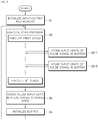
- FIG. 1 is a circuit diagram of a conventional PLC device provided with a pulse signal input circuit.
- a plurality of interrupt ports A1, ..., and An are provided at an MPU A, and a plurality of input terminals B1, ..., and Bn, to which pulse signals are input, and the plurality of interrupt ports A1, ..., and An are respectively connected to each other through a plurality of pulse signal input circuits C1, ..., and Cn in a non-conducting state.
- the plurality of pulse signal input circuits C1, ..., and Cn respectively include optical couplers C1-1, ..., and Cn-1, each of which maintains a non-conducting state and then is conducting when a signal is input, thereby outputting the input signal.
- the plurality of pulse signal input circuits C1, ..., and Cn convert pulse signals, which are input to the plurality of input terminals B1, ..., and Bn, into a complementary metal-oxide semiconductor (CMOS) level to output the converted pulse signals to the plurality of interrupt ports A1, ..., and An.
- CMOS complementary metal-oxide semiconductor
- FIG. 2 is a flow chart illustrating a procedure in which the PLC device provided with a pulse signal input circuit recognizes a pulse signal
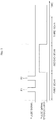
- FIG. 3 is a timing diagram between a pulse signal being input for a scan time and pulse input data stored at a pulse signal storage area.
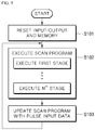
- an MPU of the PLC device firstly initializes inputs/outputs and a memory in Operation S1. Thereafter, the MPU executes a scan program from a first stage to an n th stage, thereby completing one time scan in Operation S2. At this point, when a pulse signal P1 is input to an interrupt port in the middle of a scan time in which a scan program is executed, the MPU suspends the scan program and temporarily stores an input state of the pulse signal P1 in a buffer in Operation S2-1.
- the MPU returns to the scan program to continuously execute the scan program at the suspended point in Operation S2.
- the MPU suspends the scan program and temporarily stores an input state of the pulse signal P2 in the buffer in Operation S2-2.
- the MPU After temporarily storing the input state of the pulse signal P2 in the buffer, the MPU returns to the scan program and then completes execution up to the N th e stage of the scan program in Operation S2.
- the MPU While completing the execution of the scan program from the first stage to the N th stage, the MPU stores the input states of the pulse signals P1 and P2, which are stored in the buffer as inputs of the pulse signals P1 and P2, in a pulse signal storage area as pulse input data in Operation S3.
- the MPU completes one time scan by initializing the input states of the pulse signals P1 and P2, which are stored in the buffer, in Operation S4, and then returns to Operation S1, which is described above, to repetitively perform the scan.
- the pulse input data which is stored in the pulse signal storage area, is maintained for a next scan time and is updated to the scan program.
- the conventional PLC device suspends a scan program, which is currently executed, performs a procedure of storing an input state of the input pulse signal in a buffer, and then returns to the scan program to resume the execution of the scan program.
- the conventional PLC device performs a procedure of storing an input state of a pulse signal in a buffer whenever the pulse signal is input so that there is a problem in that a scan time for performing a scan is inevitably increased as an input of the pulse signal is increased.
- the conventional PLC device should be provided with an interrupt port, which is configured to generate an interrupt signal when a pulse signal is input, at the MPU having a limited dimension so that there is a problem in that the number of input contact points of pulse signals is limited.
- the apparatus for recognizing a pulse signal includes a signal maintaining unit configured to maintain and output the pulse signal, which is input for the scan time, as a pulse maintaining signal; a signal transmission unit configured to receive the pulse maintaining signal from the signal maintaining unit and transmit the input pulse maintaining signal based on a transmission control signal; and a control unit configured to output the transmission control signal to the signal transmission unit to receive the pulse maintaining signal, and store the received pulse maintaining signal in a pulse signal storage area as pulse input data.
- the apparatus for recognizing a pulse signal includes a signal maintaining unit configured to maintain and output the pulse signal, which is input for the scan time, as a pulse maintaining signal; a signal transmission unit configured to receive the pulse maintaining signal from the signal maintaining unit and transmit the input pulse maintaining signal based on a transmission control signal; and a control unit configured to output the transmission control signal to the signal transmission unit to receive the pulse maintaining signal, and store the received pulse maintaining signal in a pulse signal storage area as pulse input data.
- a pulse signal being input for a scan time may be maintained and output as a pulse maintaining signal so that an input state of a pulse signal, which is input for a time shorter than the scan time, may be maintained up to a time in which the scan time is terminated.
- a pulse maintaining signal may be stored in a pulse signal storage area as pulse input data at a termination time of a scan time so that a pulse signal may be recognized without suspending a scan program whenever the pulse signal is input.
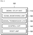
- FIG. 4 is a diagram illustrating a configuration of an apparatus 100 for recognizing a pulse signal according to one embodiment of the present disclosure
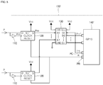
- FIG. 5 is a diagram illustrating circuit diagrams of the apparatus 100 for recognizing a pulse signal and a pulse signal input circuit C according to one embodiment of the present disclosure.
- the apparatus 100 for recognizing a pulse signal may be connected to the pulse signal input circuit C of a PLC device to recognize a pulse signal that is input to an input terminal B for a scan time.
- the pulse signal input circuit C may maintain a non-conducting state using an optical coupler C-1 and then convert a pulse signal into a complementary metal-oxide semiconductor (CMOS) level when the pulse signal is input to the input terminal B for the scan time, thereby outputting the converted pulse signal to the apparatus 100 for recognizing a pulse signal.
- CMOS complementary metal-oxide semiconductor
- the scan time refers to a time in which a micron process unit (MPU) of the PLC device begins to execute a scan program, which is programmed by a user, to terminate the execution of the scan program. That is, the MPU of the PLC device performs the scan program one time for the scan time, and then infinitely repetitively performs the scan program.
- MPU micron process unit
- the apparatus 100 for recognizing a pulse signal includes a signal delay unit 110, a signal maintaining unit 120, a signal transmission unit 130, a control unit 140, and a reset unit 150.
- the signal delay unit 110 may delay a pulse signal P, which is input for a scan time, for a preset delay time to output the pulse signal P as a pulse delay signal Pd.
- the signal delay unit 110 may delay and output the pulse delay signal Pd, which has a pulse width the same as that of the pulse signal P, by the preset delay time prior to a time in which the pulse signal P is input.
- the preset delay time may be less than the pulse width of the pulse signal P.
- the present disclosure is not limited thereto and the preset delay time may be greater than the pulse width of the pulse signal P.
- the signal delay unit 110 may be a buffer gate.
- FIG. 6 is a timing diagram of input/output signals between configurations of the apparatus 100 for recognizing a pulse signal according to one embodiment of the present disclosure.
- the signal delay unit 110 may receive the pulse signal P being input to the apparatus 100 for recognizing a pulse signal for a scan time S, and may output the pulse delay signal Pd having a pulse with W the same as that of the pulse signal P.
- the signal delay unit 110 may output the pulse delay signal Pd at a time which is delayed by a preset delay time Td with respect to a time at which the pulse signal P is input.
- the signal maintaining unit 120 may maintain the pulse signal P, which is input for the scan time S, to output the maintained pulse signal P as a pulse maintaining signal Pm.
- the signal maintaining unit 120 may maintain the pulse signal P, which is input for the scan time S, to output the maintained pulse signal P as the pulse maintaining signal Pm.
- the signal maintaining unit 120 may be a D flip-flop.
- the signal maintaining unit 120 When the signal maintaining unit 120 is a D flip-flop, it respectively receives the pulse signal P and the pulse delay signal Pd through a signal input terminal D and a clock terminal CLOCK, and outputs the pulse maintaining signal Pm through a signal output terminal Q.
- the pulse signal P of a high level H is input to the signal input terminal D of the signal maintaining unit 120, and, after the preset delay time Td from a time when the pulse signal P is input, the pulse delay signal Pd changing from a low level L to a high level H is input to the clock terminal CLOCK.
- the signal maintaining unit 120 outputs a signal, which is input to the signal input terminal D at a time when a rising edge is input to the clock terminal CLOCK, to the signal output terminal Q, and maintains the signal until a signal of a low level L is input to the reset terminal RESET.
- the signal maintaining unit 120 outputs the pulse maintaining signal Pm of a high level H to the signal output terminal Q.
- the signal maintaining unit 120 outputs the pulse maintaining signal Pm of a high level H from a time point when the pulse signal P is first input.
- the signal maintaining unit 120 may maintain and output the pulse signal P, which is input for the scan time S, as the pulse maintaining signal Pm, thereby maintaining an input state of the pulse signal P, which is input for a time shorter than the scan time S, up to a time point at which the scan time S is terminated.
- the signal transmission unit 130 may receive the pulse maintaining signal Pm from the signal maintaining unit 120, and transmit the pulse maintaining signal Pm, which is input, to the control unit 140 based on a transmission control signal CS.
- the signal transmission unit 130 may serve to transmit a signal by outputting a signal the same as the input signal based on the transmission control signal CS.
- the transmission control signal CS is a signal which is output from the control unit 140 to the signal transmission unit 130 before a preset transmission time Tt from an end time point Te of the scan time S.
- a time point before the preset transmission time Tt from the end time point Te of the scan time S is a transmission time point Tt'.
- the signal transmission unit 130 may be a bus transceiver.
- the signal transmission unit 130 When the signal transmission unit 130 is a bus transceiver, it respectively receives the pulse maintaining signal Pm and the transmission control signal CS through a signal input terminal A0 and an output enable terminal OE, and outputs the pulse maintaining signal Pm through a signal output terminal BO.
- the signal transmission unit 130 Before receiving the transmission control signal CS of a high level H from the control unit 140 through the output enable terminal OE, the signal transmission unit 130 does not transmit the pulse maintaining signal Pm, which is input to the signal input terminal AO, to the signal output terminal BO.
- the signal transmission unit 130 receives the transmission control signal CS of a low level L from the control unit 140 through the output enable terminal OE at the transmission time point Tt', and outputs the pulse maintaining signal Pm, which is input to the signal input terminal AO, to the signal output terminal BO.
- a pulse maintaining signal Pm' which is output from the signal transmission unit 130 to the control unit 140 by receiving the transmission control signal CS of a low level L from the control unit 140, is output to the control unit 140 until the transmission control signal CS of a high level H is input to the output enable terminal OE from the control unit 140.
- the control unit 140 outputs the transmission control signal CS of a low level L to the output enable terminal OE at the transmission time point Tt'.
- control unit 140 may receive the pulse maintaining signal Pm through a data bus, and may store the pulse maintaining signal Pm', which is read from the data bus and is transmitted, in a pulse signal storage area as pulse input data Pi.
- control unit 140 may output a storing control signal RD to store the pulse maintaining signal Pm', which is transmitted, in the pulse signal storage area as the pulse input data Pi.
- the control unit 140 may output the storing control signal RD of a low level L after outputting the transmission control signal CS of a low level L, and then may output the storing control signal of a high level H at an end time point Te of the scan time S.
- the control unit 140 stores the pulse maintaining signal Pm', which is transmitted at a time point when the storing control signal RD of a high level H is output, in the pulse signal storage area as the pulse input data Pi.
- control unit 140 may store the pulse maintaining signal Pm', which is transmitted at the end time point Te of the scan time S, in the pulse signal storage area as the pulse input data Pi, thereby recognizing the pulse signal P without suspending the scan program whenever the pulse signal P is input.
- the control unit 140 After storing the transmitted pulse maintaining signal Pm' as the pulse input data Pi, the control unit 140 outputs the transmission control signal CS of a high level H to the output enable terminal OE of the signal transmission unit 130 so as to block an output of the signal transmission unit 130.
- the transmission control signal CS and the storing control signal RD which are output from the control unit 140, may be output to the reset unit 150, which will be described below, in addition to the signal transmission unit 130.
- the reset unit 150 may output a reset signal R based on the transmission control signal CS and the storing control signal RD, thereby resetting an output of the signal maintaining unit 120.
- the reset unit 150 may include a first NOT gate 151, a NAND gate 152, a second NOT gate 153, and an AND gate 154.
- the first NOT gate 151 receives the transmission control signal CS and inverts and outputs a signal level thereof to the NAND gate 152.
- the first NOT gate 153 receives the transmission control signal CS and inverts and outputs a signal level thereof to the NAND gate 154.
- the AND gate 154 receives and performs an AND operation on the storing control signal RD and an output signal of the second NOT gate 153 to output the operation result to the NAND gate 152.
- the NAND gate 152 receives and performs a NAND operation on outputs of the first NOT gate 151 and the AND gate 154 to output the operation result to the reset terminal RESET of the signal maintaining unit 120 as the reset signal R.
- FIG. 7 is a timing diagram of input/output signals of the reset unit 150 according to one embodiment of the present disclosure.
- the first NOT gate 151 receives the transmission control signal CS of a low level L from the control unit 140 at the transmission time point Tt' and inverts a signal level of the transmission control signal CS to output the transmission control signal CS of the inverted signal level to the NAND gate 152.
- the transmission control signal CS which is inverted through the first NOT gate 151, is delayed for a predetermined time according to a delay characteristic of the first NOT gate 151 and then is output to the NAND gate 152.
- the control unit 140 After outputting the transmission control signal CS of a low level L, the control unit 140 outputs the storing control signal RD of a low level L.
- the second NOT gate 153 and the AND gate 154 receive the storing control signal RD of a low level L.
- the second NOT gate 153 receives the storing control signal RD of a low level L from the control unit 140 and inverts a signal level of the storing control signal RD to output the storing control signal RD of the inverted signal level to the AND gate 154.
- the storing control signal RD which is inverted through the second NOT gate 153, is delayed for a predetermined time according to a delay characteristic of the second NOT gate 153 and then is output to the AND gate 154.
- the AND gate 154 outputs a signal of a low level L to the NAND gate 152 until the end time point Te of the scan time S, at which the storing control signal RD of a high level is output from the control unit 140, and the NAND gate 152 outputs the reset signal R of a high level H to the reset terminal RESET of the signal maintaining unit 120 until the end time point Te of the scan time S.
- the signal maintaining unit 120 receives a signal of a high level H through the reset terminal RESET until the end time point Te of the scan time S and outputs the pulse maintaining signal Pm according to the signals input to the signal input terminal D and the clock terminal CLOCK as shown in the truth table.
- the control unit 140 outputs the storing control signal RD of a high level H at the end time point Te of the scan time S, and then outputs the transmission control signal CS of a high level H.
- the AND gate 154 receives the storing control signal RD of a high level H and the signal of a low level L, which is not yet inverted into a high level H in the second NOT gate 153, to output a signal of a high level H to the NAND gate 152.
- the control unit 140 outputs the transmission control signal CS of a low level L at the end time point Te of the scan time S so that the first NOT gate 151 outputs a signal of a high level H to the NAND gate 152.
- the NAND gate 152 receives only the signal of a high level H at the end time point Te of the scan time S to perform the NAND operation so that it outputs a signal of a low level L as the reset signal R.
- the reset signal R of a low level L which is output from the NAND gate 152 at the end time point Te of the scan time S, is input to the reset terminal RESET of the signal maintaining unit 120, thereby resetting an output thereof.
- the signal maintaining unit 120 resets the output thereof after the scan time S is terminated and before the next scan time S' is begun so that it may output a pulse maintaining signal when a pulse signal is input for the next scan time S'.
- the MPU of the PLC device may execute a scan program by updating the scan program, which is scheduled to be executed for the next scan time S', with the scan input data Pi stored in the scan signal storage area for the scan time S.
- FIG. 8 is a diagram illustrating a circuit diagram of an apparatus 100' for recognizing a pulse signal according to another embodiment of the present disclosure.
- a control unit 140' of the apparatus 100' for recognizing a pulse signal may receive the pulse maintaining signal Pm from the signal transmission unit 130 using a general purpose I/O (GPIO) port instead of the data bus.
- GPIO general purpose I/O
- control unit 140' may be provided with a reset output port PR and a transmission control output port PC which correspond to the GPIO port. More particularly, the reset output port PR provided at the control unit 140' may be connected to the reset terminal RESET of the signal maintaining unit 120 to output the reset signal R, thereby resetting an output of the signal maintaining unit 120.
- the apparatus 100' for recognizing a pulse signal may reset the output of the signal maintaining unit 120 at the end time point Te of the scan time S without having the reset unit 150.
- the transmission control output port PC provided at the control unit 140' may be connected to the output enable terminal OE of the signal transmission unit 130 to output the transmission control signal CS, thereby receiving the pulse maintaining signal Pm from the signal transmission unit 130.
- FIG. 9 is an operation flow chart of the PLC device provided with the apparatus 100 for recognizing a pulse signal according to one embodiment of the present disclosure.
- the MPU of the PLC device before repetitively performing a scan, the MPU of the PLC device firstly resets inputs/outputs and a memory in Operation S101. Thereafter, the MPU executes a scan program from a first stage to an n th stage, thereby completing one time scan in Operation S102. Even when a pulse signal is input for a scan time at which the MPU executes a scan program, the MPU continuously executes the scan program from the first stage to the N th stage without suspending the scan program in the middle of the execution.
- the signal delay unit of the apparatus for a pulse signal delays a pulse signal, which is input for the scan time, to output the delayed pulse signal as a pulse delay signal, and, when the pulse delay signal is input, the signal maintaining unit maintains and outputs the input pulse signal as a pulse maintaining signal until an end time point of the scan time.
- the signal transmission unit receives the transmission control signal from the control unit at a transmission time point and transmits the pulse maintaining signal, which is output from the signal maintaining unit, to the control unit, and the control unit outputs the storing control signal at the end time point of the scan to store the pulse maintaining signal, which is transmitted, in the pulse signal storage area as the pulse input data.
- the MPU updates a scan program, which is scheduled to be executed for a next scan time, with the pulse input data stored in the pulse signal storage area and completes one time scan in Operation S103.
- the PLC device provided with the apparatus 100 for a pulse signal may recognize the pulse signal without suspending the scan program, which is currently executed, to update a scan program, which is scheduled to be executed for the next scan time, with the recognized pulse signal.
- the present disclosure may maintain and output the pulse signal, which is input for the scan time, as the pulse maintaining signal so that an input state of a pulse signal, which is input for a time shorter than the scan time, may be maintained up to a time point at which the scan time is terminated.
- the present disclosure may store the pulse maintaining signal in the pulse signal storage area as the pulse input data at a termination time point of the scan time so that a pulse signal may be recognized without suspending of a scan program whenever the pulse signal is input.
Landscapes
- Engineering & Computer Science (AREA)
- Physics & Mathematics (AREA)
- Mathematical Physics (AREA)
- General Engineering & Computer Science (AREA)
- Computer Hardware Design (AREA)
- Computing Systems (AREA)
- Computer Networks & Wireless Communication (AREA)
- Multimedia (AREA)
- Signal Processing (AREA)
- General Physics & Mathematics (AREA)
- Automation & Control Theory (AREA)
- Nonlinear Science (AREA)
- Programmable Controllers (AREA)
- Logic Circuits (AREA)
Applications Claiming Priority (1)
| Application Number | Priority Date | Filing Date | Title |
|---|---|---|---|
| KR1020160133294A KR20180041319A (ko) | 2016-10-14 | 2016-10-14 | 펄스 신호 인식 장치 |
Publications (2)
| Publication Number | Publication Date |
|---|---|
| EP3309634A1 true EP3309634A1 (fr) | 2018-04-18 |
| EP3309634B1 EP3309634B1 (fr) | 2019-09-04 |
Family
ID=58544697
Family Applications (1)
| Application Number | Title | Priority Date | Filing Date |
|---|---|---|---|
| EP17161326.8A Active EP3309634B1 (fr) | 2016-10-14 | 2017-03-16 | Appareil de reconnaissance de signal d'impulsion |
Country Status (6)
| Country | Link |
|---|---|
| US (1) | US10110236B2 (fr) |
| EP (1) | EP3309634B1 (fr) |
| JP (1) | JP6377793B2 (fr) |
| KR (1) | KR20180041319A (fr) |
| CN (1) | CN107959484A (fr) |
| ES (1) | ES2756701T3 (fr) |
Citations (3)
| Publication number | Priority date | Publication date | Assignee | Title |
|---|---|---|---|---|
| US5008802A (en) * | 1988-01-11 | 1991-04-16 | Mitsubishi Denki K.K. | Dynamic input method and apparatus for programmable controller |
| EP0447776A2 (fr) * | 1990-03-19 | 1991-09-25 | Hitachi, Ltd. | Automate programmable |
| US6904471B2 (en) * | 1999-03-30 | 2005-06-07 | Siemens Energy & Automation, Inc. | Programmable logic controller customized function call method, system and apparatus |
Family Cites Families (21)
| Publication number | Priority date | Publication date | Assignee | Title |
|---|---|---|---|---|
| JPS60238902A (ja) | 1984-05-11 | 1985-11-27 | Sharp Corp | 高速パルスラツチユニツト |
| JPH0810978Y2 (ja) | 1990-11-29 | 1996-03-29 | 横河電機株式会社 | ステータス信号読込み回路 |
| US5221865A (en) * | 1991-06-21 | 1993-06-22 | Crosspoint Solutions, Inc. | Programmable input/output buffer circuit with test capability |
| JP3085318B2 (ja) | 1991-06-25 | 2000-09-04 | 株式会社安川電機 | プログラマブル・コントローラにおける制御プログラム実行方式 |
| JPH0530905U (ja) | 1991-09-27 | 1993-04-23 | 横河電機株式会社 | ステータス読み込み回路 |
| JP3298018B2 (ja) | 1992-04-09 | 2002-07-02 | 光洋電子工業株式会社 | プログラマブルコントローラ |
| JPH1172541A (ja) * | 1997-06-10 | 1999-03-16 | Altera Corp | プログラマブル集積回路を構成する方法、プログラマブル集積回路、jtag回路の使用、およびjtag命令レジスタに入力される命令の使用 |
| JP2001160873A (ja) * | 1999-12-02 | 2001-06-12 | Canon Inc | 画像読取り装置、その制御方法、及びその制御プログラムを格納したコンピュータにより読取り可能な記録媒体 |
| JP2001202110A (ja) | 2000-01-21 | 2001-07-27 | Hitachi Ltd | プログラマブルコントローラ |
| JP2002163008A (ja) | 2000-11-27 | 2002-06-07 | Matsushita Electric Works Ltd | プログラマブルコントローラ暴走検出回路およびその方法 |
| US6614278B2 (en) * | 2001-05-29 | 2003-09-02 | Samsung Electronics Co., Ltd. | Pulsed signal transition delay adjusting circuit |
| KR100972509B1 (ko) | 2003-03-19 | 2010-07-28 | 엘에스산전 주식회사 | 피엘씨의 스캔 프로그램 제어 방법 |
| US7019577B2 (en) * | 2003-07-29 | 2006-03-28 | Lattice Semiconductor Corporation | Clock generator |
| US7256634B2 (en) * | 2005-07-06 | 2007-08-14 | Transmeta Corporation | Elastic pipeline latch with a safe mode |
| CN100568728C (zh) * | 2005-10-31 | 2009-12-09 | 中兴通讯股份有限公司 | 一种时钟信号检测电路 |
| US7459931B1 (en) * | 2006-04-05 | 2008-12-02 | Lattice Semiconductor Corporation | Programmable logic devices with transparent field reconfiguration |
| CN101742078B (zh) * | 2008-01-31 | 2011-11-23 | 华为技术有限公司 | 一种同步时钟提取装置和方法 |
| CN201349208Y (zh) * | 2008-12-23 | 2009-11-18 | 康佳集团股份有限公司 | 一种fpga多模式配置电路 |
| CN101447786B (zh) * | 2008-12-29 | 2010-11-10 | 北京时代民芯科技有限公司 | 一种抗单粒子瞬态缓冲器单元电路 |
| CN103248342B (zh) * | 2013-05-16 | 2015-12-09 | 中国电子科技集团公司第四十一研究所 | 一种脉冲延迟电路及扫描方法 |
| KR101480642B1 (ko) * | 2013-10-15 | 2015-01-09 | 엘에스산전 주식회사 | 이벤트 입력모듈 |
-
2016
- 2016-10-14 KR KR1020160133294A patent/KR20180041319A/ko not_active Withdrawn
-
2017
- 2017-03-16 EP EP17161326.8A patent/EP3309634B1/fr active Active
- 2017-03-16 ES ES17161326T patent/ES2756701T3/es active Active
- 2017-03-20 US US15/463,777 patent/US10110236B2/en not_active Expired - Fee Related
- 2017-03-22 JP JP2017056472A patent/JP6377793B2/ja not_active Expired - Fee Related
- 2017-03-29 CN CN201710195822.3A patent/CN107959484A/zh active Pending
Patent Citations (3)
| Publication number | Priority date | Publication date | Assignee | Title |
|---|---|---|---|---|
| US5008802A (en) * | 1988-01-11 | 1991-04-16 | Mitsubishi Denki K.K. | Dynamic input method and apparatus for programmable controller |
| EP0447776A2 (fr) * | 1990-03-19 | 1991-09-25 | Hitachi, Ltd. | Automate programmable |
| US6904471B2 (en) * | 1999-03-30 | 2005-06-07 | Siemens Energy & Automation, Inc. | Programmable logic controller customized function call method, system and apparatus |
Also Published As
| Publication number | Publication date |
|---|---|
| ES2756701T3 (es) | 2020-04-27 |
| KR20180041319A (ko) | 2018-04-24 |
| CN107959484A (zh) | 2018-04-24 |
| JP2018063691A (ja) | 2018-04-19 |
| US10110236B2 (en) | 2018-10-23 |
| JP6377793B2 (ja) | 2018-08-22 |
| US20180109261A1 (en) | 2018-04-19 |
| EP3309634B1 (fr) | 2019-09-04 |
Similar Documents
| Publication | Publication Date | Title |
|---|---|---|
| CN105094976A (zh) | 一种中断控制方法和中断控制器 | |
| US9910420B2 (en) | Expansion module for programmable logic controller using USB communication | |
| US20210103465A1 (en) | Scheduling of External Block Based Data Processing Tasks on a Hardware Thread Scheduler | |
| EP3309634A1 (fr) | Appareil de reconnaissance de signal d'impulsion | |
| KR101205589B1 (ko) | 동기형 메모리 장치 및 버스트 기입 동작의 제어 방법 | |
| CN111103959A (zh) | 寄存器复位系统及芯片 | |
| KR100313945B1 (ko) | 다단 인터럽트 제어 장치 | |
| US9361258B2 (en) | Common interface/conditional access module and method of transmitting data between common interface card and integrated circuit chip thereof | |
| US5495196A (en) | User controlled reset circuit with fast recovery | |
| CN110788458A (zh) | 螺柱焊设备的控制方法与系统、存储介质、及电子设备 | |
| CN106325893A (zh) | 逻辑器件配置方法及装置 | |
| CN115457998B (zh) | 一种mipi rffe接口地址扩展电路、方法和相关设备 | |
| CN223757268U (zh) | 一种存储器驱动电路和存储器 | |
| TWI766521B (zh) | 解決通訊介面暫態脈衝輸出的電子裝置及方法 | |
| US8436651B2 (en) | Command control circuit for semiconductor integrated device | |
| KR0154798B1 (ko) | 글리치에 무관한 제어신호 발생회로 | |
| JPS6059441A (ja) | デ−タ制御回路 | |
| US10372644B2 (en) | Programmable controller | |
| US8723579B2 (en) | Timing generation circuit | |
| JP5071655B2 (ja) | 制御回路 | |
| CN121012466A (zh) | 一种时钟产生电路、时钟产生方法以及电子设备 | |
| CN117559985A (zh) | 控制电路和半导体存储器 | |
| KR200298423Y1 (ko) | 다수 프로세서의 주변 장치 액세스를 위한 조정 논리회로 | |
| US20160011263A1 (en) | Semiconductor apparatus | |
| KR19990032841A (ko) | 우선처리 제어장치 |
Legal Events
| Date | Code | Title | Description |
|---|---|---|---|
| PUAI | Public reference made under article 153(3) epc to a published international application that has entered the european phase |
Free format text: ORIGINAL CODE: 0009012 |
|
| STAA | Information on the status of an ep patent application or granted ep patent |
Free format text: STATUS: THE APPLICATION HAS BEEN PUBLISHED |
|
| AK | Designated contracting states |
Kind code of ref document: A1 Designated state(s): AL AT BE BG CH CY CZ DE DK EE ES FI FR GB GR HR HU IE IS IT LI LT LU LV MC MK MT NL NO PL PT RO RS SE SI SK SM TR |
|
| AX | Request for extension of the european patent |
Extension state: BA ME |
|
| STAA | Information on the status of an ep patent application or granted ep patent |
Free format text: STATUS: REQUEST FOR EXAMINATION WAS MADE |
|
| STAA | Information on the status of an ep patent application or granted ep patent |
Free format text: STATUS: EXAMINATION IS IN PROGRESS |
|
| 17P | Request for examination filed |
Effective date: 20180518 |
|
| RBV | Designated contracting states (corrected) |
Designated state(s): AL AT BE BG CH CY CZ DE DK EE ES FI FR GB GR HR HU IE IS IT LI LT LU LV MC MK MT NL NO PL PT RO RS SE SI SK SM TR |
|
| 17Q | First examination report despatched |
Effective date: 20180618 |
|
| GRAP | Despatch of communication of intention to grant a patent |
Free format text: ORIGINAL CODE: EPIDOSNIGR1 |
|
| STAA | Information on the status of an ep patent application or granted ep patent |
Free format text: STATUS: GRANT OF PATENT IS INTENDED |
|
| INTG | Intention to grant announced |
Effective date: 20190404 |
|
| GRAS | Grant fee paid |
Free format text: ORIGINAL CODE: EPIDOSNIGR3 |
|
| GRAA | (expected) grant |
Free format text: ORIGINAL CODE: 0009210 |
|
| STAA | Information on the status of an ep patent application or granted ep patent |
Free format text: STATUS: THE PATENT HAS BEEN GRANTED |
|
| AK | Designated contracting states |
Kind code of ref document: B1 Designated state(s): AL AT BE BG CH CY CZ DE DK EE ES FI FR GB GR HR HU IE IS IT LI LT LU LV MC MK MT NL NO PL PT RO RS SE SI SK SM TR |
|
| REG | Reference to a national code |
Ref country code: GB Ref legal event code: FG4D |
|
| REG | Reference to a national code |
Ref country code: CH Ref legal event code: EP |
|
| REG | Reference to a national code |
Ref country code: AT Ref legal event code: REF Ref document number: 1176237 Country of ref document: AT Kind code of ref document: T Effective date: 20190915 |
|
| REG | Reference to a national code |
Ref country code: DE Ref legal event code: R096 Ref document number: 602017006634 Country of ref document: DE |
|
| REG | Reference to a national code |
Ref country code: IE Ref legal event code: FG4D |
|
| REG | Reference to a national code |
Ref country code: NL Ref legal event code: MP Effective date: 20190904 |
|
| REG | Reference to a national code |
Ref country code: LT Ref legal event code: MG4D |
|
| PG25 | Lapsed in a contracting state [announced via postgrant information from national office to epo] |
Ref country code: FI Free format text: LAPSE BECAUSE OF FAILURE TO SUBMIT A TRANSLATION OF THE DESCRIPTION OR TO PAY THE FEE WITHIN THE PRESCRIBED TIME-LIMIT Effective date: 20190904 Ref country code: NO Free format text: LAPSE BECAUSE OF FAILURE TO SUBMIT A TRANSLATION OF THE DESCRIPTION OR TO PAY THE FEE WITHIN THE PRESCRIBED TIME-LIMIT Effective date: 20191204 Ref country code: SE Free format text: LAPSE BECAUSE OF FAILURE TO SUBMIT A TRANSLATION OF THE DESCRIPTION OR TO PAY THE FEE WITHIN THE PRESCRIBED TIME-LIMIT Effective date: 20190904 Ref country code: BG Free format text: LAPSE BECAUSE OF FAILURE TO SUBMIT A TRANSLATION OF THE DESCRIPTION OR TO PAY THE FEE WITHIN THE PRESCRIBED TIME-LIMIT Effective date: 20191204 Ref country code: HR Free format text: LAPSE BECAUSE OF FAILURE TO SUBMIT A TRANSLATION OF THE DESCRIPTION OR TO PAY THE FEE WITHIN THE PRESCRIBED TIME-LIMIT Effective date: 20190904 Ref country code: LT Free format text: LAPSE BECAUSE OF FAILURE TO SUBMIT A TRANSLATION OF THE DESCRIPTION OR TO PAY THE FEE WITHIN THE PRESCRIBED TIME-LIMIT Effective date: 20190904 |
|
| PG25 | Lapsed in a contracting state [announced via postgrant information from national office to epo] |
Ref country code: RS Free format text: LAPSE BECAUSE OF FAILURE TO SUBMIT A TRANSLATION OF THE DESCRIPTION OR TO PAY THE FEE WITHIN THE PRESCRIBED TIME-LIMIT Effective date: 20190904 Ref country code: LV Free format text: LAPSE BECAUSE OF FAILURE TO SUBMIT A TRANSLATION OF THE DESCRIPTION OR TO PAY THE FEE WITHIN THE PRESCRIBED TIME-LIMIT Effective date: 20190904 Ref country code: GR Free format text: LAPSE BECAUSE OF FAILURE TO SUBMIT A TRANSLATION OF THE DESCRIPTION OR TO PAY THE FEE WITHIN THE PRESCRIBED TIME-LIMIT Effective date: 20191205 Ref country code: AL Free format text: LAPSE BECAUSE OF FAILURE TO SUBMIT A TRANSLATION OF THE DESCRIPTION OR TO PAY THE FEE WITHIN THE PRESCRIBED TIME-LIMIT Effective date: 20190904 |
|
| PGFP | Annual fee paid to national office [announced via postgrant information from national office to epo] |
Ref country code: FR Payment date: 20191223 Year of fee payment: 4 |
|
| REG | Reference to a national code |
Ref country code: AT Ref legal event code: MK05 Ref document number: 1176237 Country of ref document: AT Kind code of ref document: T Effective date: 20190904 |
|
| REG | Reference to a national code |
Ref country code: ES Ref legal event code: FG2A Ref document number: 2756701 Country of ref document: ES Kind code of ref document: T3 Effective date: 20200427 |
|
| PG25 | Lapsed in a contracting state [announced via postgrant information from national office to epo] |
Ref country code: EE Free format text: LAPSE BECAUSE OF FAILURE TO SUBMIT A TRANSLATION OF THE DESCRIPTION OR TO PAY THE FEE WITHIN THE PRESCRIBED TIME-LIMIT Effective date: 20190904 Ref country code: NL Free format text: LAPSE BECAUSE OF FAILURE TO SUBMIT A TRANSLATION OF THE DESCRIPTION OR TO PAY THE FEE WITHIN THE PRESCRIBED TIME-LIMIT Effective date: 20190904 Ref country code: PL Free format text: LAPSE BECAUSE OF FAILURE TO SUBMIT A TRANSLATION OF THE DESCRIPTION OR TO PAY THE FEE WITHIN THE PRESCRIBED TIME-LIMIT Effective date: 20190904 Ref country code: PT Free format text: LAPSE BECAUSE OF FAILURE TO SUBMIT A TRANSLATION OF THE DESCRIPTION OR TO PAY THE FEE WITHIN THE PRESCRIBED TIME-LIMIT Effective date: 20200106 Ref country code: RO Free format text: LAPSE BECAUSE OF FAILURE TO SUBMIT A TRANSLATION OF THE DESCRIPTION OR TO PAY THE FEE WITHIN THE PRESCRIBED TIME-LIMIT Effective date: 20190904 Ref country code: AT Free format text: LAPSE BECAUSE OF FAILURE TO SUBMIT A TRANSLATION OF THE DESCRIPTION OR TO PAY THE FEE WITHIN THE PRESCRIBED TIME-LIMIT Effective date: 20190904 |
|
| PGFP | Annual fee paid to national office [announced via postgrant information from national office to epo] |
Ref country code: IT Payment date: 20200331 Year of fee payment: 4 Ref country code: DE Payment date: 20191220 Year of fee payment: 4 |
|
| PG25 | Lapsed in a contracting state [announced via postgrant information from national office to epo] |
Ref country code: SM Free format text: LAPSE BECAUSE OF FAILURE TO SUBMIT A TRANSLATION OF THE DESCRIPTION OR TO PAY THE FEE WITHIN THE PRESCRIBED TIME-LIMIT Effective date: 20190904 Ref country code: CZ Free format text: LAPSE BECAUSE OF FAILURE TO SUBMIT A TRANSLATION OF THE DESCRIPTION OR TO PAY THE FEE WITHIN THE PRESCRIBED TIME-LIMIT Effective date: 20190904 Ref country code: IS Free format text: LAPSE BECAUSE OF FAILURE TO SUBMIT A TRANSLATION OF THE DESCRIPTION OR TO PAY THE FEE WITHIN THE PRESCRIBED TIME-LIMIT Effective date: 20200224 Ref country code: SK Free format text: LAPSE BECAUSE OF FAILURE TO SUBMIT A TRANSLATION OF THE DESCRIPTION OR TO PAY THE FEE WITHIN THE PRESCRIBED TIME-LIMIT Effective date: 20190904 |
|
| REG | Reference to a national code |
Ref country code: DE Ref legal event code: R097 Ref document number: 602017006634 Country of ref document: DE |
|
| PLBE | No opposition filed within time limit |
Free format text: ORIGINAL CODE: 0009261 |
|
| STAA | Information on the status of an ep patent application or granted ep patent |
Free format text: STATUS: NO OPPOSITION FILED WITHIN TIME LIMIT |
|
| PG2D | Information on lapse in contracting state deleted |
Ref country code: IS |
|
| PG25 | Lapsed in a contracting state [announced via postgrant information from national office to epo] |
Ref country code: DK Free format text: LAPSE BECAUSE OF FAILURE TO SUBMIT A TRANSLATION OF THE DESCRIPTION OR TO PAY THE FEE WITHIN THE PRESCRIBED TIME-LIMIT Effective date: 20190904 Ref country code: IS Free format text: LAPSE BECAUSE OF FAILURE TO SUBMIT A TRANSLATION OF THE DESCRIPTION OR TO PAY THE FEE WITHIN THE PRESCRIBED TIME-LIMIT Effective date: 20200105 |
|
| PGFP | Annual fee paid to national office [announced via postgrant information from national office to epo] |
Ref country code: ES Payment date: 20200414 Year of fee payment: 4 |
|
| 26N | No opposition filed |
Effective date: 20200605 |
|
| PG25 | Lapsed in a contracting state [announced via postgrant information from national office to epo] |
Ref country code: SI Free format text: LAPSE BECAUSE OF FAILURE TO SUBMIT A TRANSLATION OF THE DESCRIPTION OR TO PAY THE FEE WITHIN THE PRESCRIBED TIME-LIMIT Effective date: 20190904 |
|
| PG25 | Lapsed in a contracting state [announced via postgrant information from national office to epo] |
Ref country code: MC Free format text: LAPSE BECAUSE OF FAILURE TO SUBMIT A TRANSLATION OF THE DESCRIPTION OR TO PAY THE FEE WITHIN THE PRESCRIBED TIME-LIMIT Effective date: 20190904 |
|
| REG | Reference to a national code |
Ref country code: CH Ref legal event code: PL |
|
| REG | Reference to a national code |
Ref country code: BE Ref legal event code: MM Effective date: 20200331 |
|
| PG25 | Lapsed in a contracting state [announced via postgrant information from national office to epo] |
Ref country code: LU Free format text: LAPSE BECAUSE OF NON-PAYMENT OF DUE FEES Effective date: 20200316 |
|
| PG25 | Lapsed in a contracting state [announced via postgrant information from national office to epo] |
Ref country code: LI Free format text: LAPSE BECAUSE OF NON-PAYMENT OF DUE FEES Effective date: 20200331 Ref country code: IE Free format text: LAPSE BECAUSE OF NON-PAYMENT OF DUE FEES Effective date: 20200316 Ref country code: CH Free format text: LAPSE BECAUSE OF NON-PAYMENT OF DUE FEES Effective date: 20200331 |
|
| PG25 | Lapsed in a contracting state [announced via postgrant information from national office to epo] |
Ref country code: BE Free format text: LAPSE BECAUSE OF NON-PAYMENT OF DUE FEES Effective date: 20200331 |
|
| REG | Reference to a national code |
Ref country code: DE Ref legal event code: R119 Ref document number: 602017006634 Country of ref document: DE |
|
| GBPC | Gb: european patent ceased through non-payment of renewal fee |
Effective date: 20210316 |
|
| PG25 | Lapsed in a contracting state [announced via postgrant information from national office to epo] |
Ref country code: DE Free format text: LAPSE BECAUSE OF NON-PAYMENT OF DUE FEES Effective date: 20211001 Ref country code: GB Free format text: LAPSE BECAUSE OF NON-PAYMENT OF DUE FEES Effective date: 20210316 Ref country code: FR Free format text: LAPSE BECAUSE OF NON-PAYMENT OF DUE FEES Effective date: 20210331 |
|
| PG25 | Lapsed in a contracting state [announced via postgrant information from national office to epo] |
Ref country code: IT Free format text: LAPSE BECAUSE OF NON-PAYMENT OF DUE FEES Effective date: 20210316 |
|
| REG | Reference to a national code |
Ref country code: ES Ref legal event code: FD2A Effective date: 20220523 |
|
| PG25 | Lapsed in a contracting state [announced via postgrant information from national office to epo] |
Ref country code: TR Free format text: LAPSE BECAUSE OF FAILURE TO SUBMIT A TRANSLATION OF THE DESCRIPTION OR TO PAY THE FEE WITHIN THE PRESCRIBED TIME-LIMIT Effective date: 20190904 Ref country code: MT Free format text: LAPSE BECAUSE OF FAILURE TO SUBMIT A TRANSLATION OF THE DESCRIPTION OR TO PAY THE FEE WITHIN THE PRESCRIBED TIME-LIMIT Effective date: 20190904 Ref country code: CY Free format text: LAPSE BECAUSE OF FAILURE TO SUBMIT A TRANSLATION OF THE DESCRIPTION OR TO PAY THE FEE WITHIN THE PRESCRIBED TIME-LIMIT Effective date: 20190904 |
|
| PG25 | Lapsed in a contracting state [announced via postgrant information from national office to epo] |
Ref country code: MK Free format text: LAPSE BECAUSE OF FAILURE TO SUBMIT A TRANSLATION OF THE DESCRIPTION OR TO PAY THE FEE WITHIN THE PRESCRIBED TIME-LIMIT Effective date: 20190904 |
|
| PG25 | Lapsed in a contracting state [announced via postgrant information from national office to epo] |
Ref country code: ES Free format text: LAPSE BECAUSE OF NON-PAYMENT OF DUE FEES Effective date: 20210317 |