EP3312596A1 - Procédé et dispositif d'observation de bande de matériau et d'inspection de bande de matériau - Google Patents
Procédé et dispositif d'observation de bande de matériau et d'inspection de bande de matériau Download PDFInfo
- Publication number
- EP3312596A1 EP3312596A1 EP17195965.3A EP17195965A EP3312596A1 EP 3312596 A1 EP3312596 A1 EP 3312596A1 EP 17195965 A EP17195965 A EP 17195965A EP 3312596 A1 EP3312596 A1 EP 3312596A1
- Authority
- EP
- European Patent Office
- Prior art keywords
- binning
- web
- matrix chip
- time
- control unit
- Prior art date
- Legal status (The legal status is an assumption and is not a legal conclusion. Google has not performed a legal analysis and makes no representation as to the accuracy of the status listed.)
- Granted
Links
Images



Classifications
-
- G—PHYSICS
- G06—COMPUTING OR CALCULATING; COUNTING
- G06T—IMAGE DATA PROCESSING OR GENERATION, IN GENERAL
- G06T7/00—Image analysis
- G06T7/0002—Inspection of images, e.g. flaw detection
- G06T7/0004—Industrial image inspection
-
- G—PHYSICS
- G01—MEASURING; TESTING
- G01N—INVESTIGATING OR ANALYSING MATERIALS BY DETERMINING THEIR CHEMICAL OR PHYSICAL PROPERTIES
- G01N21/00—Investigating or analysing materials by the use of optical means, i.e. using sub-millimetre waves, infrared, visible or ultraviolet light
- G01N21/84—Systems specially adapted for particular applications
- G01N21/88—Investigating the presence of flaws or contamination
- G01N21/8851—Scan or image signal processing specially adapted therefor, e.g. for scan signal adjustment, for detecting different kinds of defects, for compensating for structures, markings, edges
-
- G—PHYSICS
- G01—MEASURING; TESTING
- G01N—INVESTIGATING OR ANALYSING MATERIALS BY DETERMINING THEIR CHEMICAL OR PHYSICAL PROPERTIES
- G01N21/00—Investigating or analysing materials by the use of optical means, i.e. using sub-millimetre waves, infrared, visible or ultraviolet light
- G01N21/84—Systems specially adapted for particular applications
- G01N21/88—Investigating the presence of flaws or contamination
- G01N21/89—Investigating the presence of flaws or contamination in moving material, e.g. running paper or textiles
-
- G—PHYSICS
- G01—MEASURING; TESTING
- G01N—INVESTIGATING OR ANALYSING MATERIALS BY DETERMINING THEIR CHEMICAL OR PHYSICAL PROPERTIES
- G01N21/00—Investigating or analysing materials by the use of optical means, i.e. using sub-millimetre waves, infrared, visible or ultraviolet light
- G01N21/84—Systems specially adapted for particular applications
- G01N21/88—Investigating the presence of flaws or contamination
- G01N21/89—Investigating the presence of flaws or contamination in moving material, e.g. running paper or textiles
- G01N21/8901—Optical details; Scanning details
-
- G—PHYSICS
- G01—MEASURING; TESTING
- G01N—INVESTIGATING OR ANALYSING MATERIALS BY DETERMINING THEIR CHEMICAL OR PHYSICAL PROPERTIES
- G01N21/00—Investigating or analysing materials by the use of optical means, i.e. using sub-millimetre waves, infrared, visible or ultraviolet light
- G01N21/84—Systems specially adapted for particular applications
- G01N21/88—Investigating the presence of flaws or contamination
- G01N21/89—Investigating the presence of flaws or contamination in moving material, e.g. running paper or textiles
- G01N21/8901—Optical details; Scanning details
- G01N21/8903—Optical details; Scanning details using a multiple detector array
-
- G—PHYSICS
- G06—COMPUTING OR CALCULATING; COUNTING
- G06T—IMAGE DATA PROCESSING OR GENERATION, IN GENERAL
- G06T7/00—Image analysis
- G06T7/70—Determining position or orientation of objects or cameras
-
- H—ELECTRICITY
- H04—ELECTRIC COMMUNICATION TECHNIQUE
- H04N—PICTORIAL COMMUNICATION, e.g. TELEVISION
- H04N23/00—Cameras or camera modules comprising electronic image sensors; Control thereof
- H04N23/60—Control of cameras or camera modules
- H04N23/69—Control of means for changing angle of the field of view, e.g. optical zoom objectives or electronic zooming
-
- H—ELECTRICITY
- H04—ELECTRIC COMMUNICATION TECHNIQUE
- H04N—PICTORIAL COMMUNICATION, e.g. TELEVISION
- H04N23/00—Cameras or camera modules comprising electronic image sensors; Control thereof
- H04N23/90—Arrangement of cameras or camera modules, e.g. multiple cameras in TV studios or sports stadiums
-
- H—ELECTRICITY
- H04—ELECTRIC COMMUNICATION TECHNIQUE
- H04N—PICTORIAL COMMUNICATION, e.g. TELEVISION
- H04N25/00—Circuitry of solid-state image sensors [SSIS]; Control thereof
- H04N25/40—Extracting pixel data from image sensors by controlling scanning circuits, e.g. by modifying the number of pixels sampled or to be sampled
- H04N25/44—Extracting pixel data from image sensors by controlling scanning circuits, e.g. by modifying the number of pixels sampled or to be sampled by partially reading an SSIS array
- H04N25/443—Extracting pixel data from image sensors by controlling scanning circuits, e.g. by modifying the number of pixels sampled or to be sampled by partially reading an SSIS array by reading pixels from selected two-dimensional [2D] regions of the array, e.g. for windowing or digital zooming
-
- H—ELECTRICITY
- H04—ELECTRIC COMMUNICATION TECHNIQUE
- H04N—PICTORIAL COMMUNICATION, e.g. TELEVISION
- H04N25/00—Circuitry of solid-state image sensors [SSIS]; Control thereof
- H04N25/40—Extracting pixel data from image sensors by controlling scanning circuits, e.g. by modifying the number of pixels sampled or to be sampled
- H04N25/46—Extracting pixel data from image sensors by controlling scanning circuits, e.g. by modifying the number of pixels sampled or to be sampled by combining or binning pixels
-
- G—PHYSICS
- G01—MEASURING; TESTING
- G01N—INVESTIGATING OR ANALYSING MATERIALS BY DETERMINING THEIR CHEMICAL OR PHYSICAL PROPERTIES
- G01N21/00—Investigating or analysing materials by the use of optical means, i.e. using sub-millimetre waves, infrared, visible or ultraviolet light
- G01N21/84—Systems specially adapted for particular applications
- G01N21/88—Investigating the presence of flaws or contamination
- G01N21/8851—Scan or image signal processing specially adapted therefor, e.g. for scan signal adjustment, for detecting different kinds of defects, for compensating for structures, markings, edges
- G01N2021/8854—Grading and classifying of flaws
- G01N2021/8861—Determining coordinates of flaws
-
- G—PHYSICS
- G01—MEASURING; TESTING
- G01N—INVESTIGATING OR ANALYSING MATERIALS BY DETERMINING THEIR CHEMICAL OR PHYSICAL PROPERTIES
- G01N21/00—Investigating or analysing materials by the use of optical means, i.e. using sub-millimetre waves, infrared, visible or ultraviolet light
- G01N21/84—Systems specially adapted for particular applications
- G01N21/88—Investigating the presence of flaws or contamination
- G01N21/8851—Scan or image signal processing specially adapted therefor, e.g. for scan signal adjustment, for detecting different kinds of defects, for compensating for structures, markings, edges
- G01N2021/8854—Grading and classifying of flaws
- G01N2021/8861—Determining coordinates of flaws
- G01N2021/8864—Mapping zones of defects
-
- G—PHYSICS
- G01—MEASURING; TESTING
- G01N—INVESTIGATING OR ANALYSING MATERIALS BY DETERMINING THEIR CHEMICAL OR PHYSICAL PROPERTIES
- G01N21/00—Investigating or analysing materials by the use of optical means, i.e. using sub-millimetre waves, infrared, visible or ultraviolet light
- G01N21/84—Systems specially adapted for particular applications
- G01N21/88—Investigating the presence of flaws or contamination
- G01N21/8851—Scan or image signal processing specially adapted therefor, e.g. for scan signal adjustment, for detecting different kinds of defects, for compensating for structures, markings, edges
- G01N2021/8854—Grading and classifying of flaws
- G01N2021/8867—Grading and classifying of flaws using sequentially two or more inspection runs, e.g. coarse and fine, or detecting then analysing
-
- G—PHYSICS
- G01—MEASURING; TESTING
- G01N—INVESTIGATING OR ANALYSING MATERIALS BY DETERMINING THEIR CHEMICAL OR PHYSICAL PROPERTIES
- G01N21/00—Investigating or analysing materials by the use of optical means, i.e. using sub-millimetre waves, infrared, visible or ultraviolet light
- G01N21/84—Systems specially adapted for particular applications
- G01N21/88—Investigating the presence of flaws or contamination
- G01N21/8851—Scan or image signal processing specially adapted therefor, e.g. for scan signal adjustment, for detecting different kinds of defects, for compensating for structures, markings, edges
- G01N2021/8887—Scan or image signal processing specially adapted therefor, e.g. for scan signal adjustment, for detecting different kinds of defects, for compensating for structures, markings, edges based on image processing techniques
-
- G—PHYSICS
- G06—COMPUTING OR CALCULATING; COUNTING
- G06T—IMAGE DATA PROCESSING OR GENERATION, IN GENERAL
- G06T2207/00—Indexing scheme for image analysis or image enhancement
- G06T2207/10—Image acquisition modality
- G06T2207/10141—Special mode during image acquisition
- G06T2207/10148—Varying focus
-
- G—PHYSICS
- G06—COMPUTING OR CALCULATING; COUNTING
- G06T—IMAGE DATA PROCESSING OR GENERATION, IN GENERAL
- G06T2207/00—Indexing scheme for image analysis or image enhancement
- G06T2207/10—Image acquisition modality
- G06T2207/10141—Special mode during image acquisition
- G06T2207/10152—Varying illumination
-
- G—PHYSICS
- G06—COMPUTING OR CALCULATING; COUNTING
- G06T—IMAGE DATA PROCESSING OR GENERATION, IN GENERAL
- G06T2207/00—Indexing scheme for image analysis or image enhancement
- G06T2207/30—Subject of image; Context of image processing
- G06T2207/30108—Industrial image inspection
- G06T2207/30124—Fabrics; Textile; Paper
Definitions
- the present invention relates to a method and apparatus for web web inspection and web inspection for machines with continuously moving products, such as webs.
- an observation and / or automated quality assurance after printing is of great importance to check the printing result.
- support for visual monitoring by an operator may also be provided.
- the webs are passed under observation or inspection systems that record images of the webs. These images can be checked by an operator or automatically.
- zoom functionalities are provided. These are in known applications via zoom lenses or systems with multiple cameras (so-called Dualview camera systems) or additional movable cameras for detail shots (see, for example DE 10 2012 101 310 B3 ) provided.
- the present invention relates to a method for observation and / or inspection of webs of material and according to claim 1 and an apparatus for observation and / or inspection of webs according to claim 21.
- the method according to the invention for observing and / or inspecting material webs which move in the direction of a material web length y and / or in the direction of a material web width x comprises the following steps: taking a first photograph of a first portion of a material web at a first time with a camera comprising a matrix chip having a binning function, and making a second shot of a second portion of the web at a second time with the camera, wherein a first binning step is used for the first shot, wherein each of a first number of pixels of the Matrix chips is combined using the binning function and for the second recording, a second binning stage is used in which each a second number of pixels of the matrix chip is combined using the binning function and, wherein the first number of pixels each be summarized higher or lower is al s is the second number of pixels that are combined, resulting in a physical zoom function for the second shot.
- An advantage of this method is in particular that without physical complex devices, such as a zoom lens or
- first section and the second section may be two identical or corresponding material web sections, or the second section may be a partial section or a corresponding section of the first section of the material web.
- a first active region of the matrix chip can be used for the first image in order to cover a first viewing region and for the second image a second active region of the matrix chip can be used to cover a second visual region ,
- the first active area and corresponding to the first viewing area can be the same size or larger than the second active area and correspondingly the second viewing area.
- the second active region may be the same active region of the matrix chip as the first active region or part of the first active region.
- the second active region may be arranged within the first active region.
- An advantage of this method is, for example, reducing the amount of data and the required computing power through the application of the binning function and a "region of interest" (ROI) function, since only the respectively required resolution or the respectively required field of view is recorded and processed , A reduced data load in turn also allows an increase in the image capture frequency (frames per second: "FPS").
- the method may also include the steps of: presenting the first shot to a user, creating the second shot in response to a user input, and presenting the second shot to the user.
- the second binning stage and, optionally, the second viewing area may be selected depending on the user input.
- the first active region and the second active region can not be identical.
- the first area and the second area may overlap or not overlap.
- the method may further comprise the steps of: evaluating the first shot and determining a position of at least one error on the web and selecting the second binning level and / or the second active area based on the position of the fault on the material web. This is advantageous if the viewing range in the x and y directions can be restricted to the position of the error. Then it is possible, for example, to further reduce the binning level and thus achieve a higher resolution for the zoom function without increasing the data amount of the second recording.
- the second shot may also be created at the second time based on the position of the error.
- the second active area and / or the second time of the second recordings can also be determined as a function of a material web speed with which the material web moves.
- a position in the direction of the material web length y, a position in the direction of the material web width x and / or a size can be determined based on the position of the defect and the size of the defect.
- the position of a plurality of errors can also be determined and a corresponding plurality of second images can be created.
- the matrix chip can be divided into first and second parts, wherein the first part works with the first binning stage and is used for the first recording and the second part with the second binning Stage works and is used for the second recording.
- the second part can lie in the direction of the web movement behind the first part. It can be provided that the second part is activated only if an error was found in the first recording.
- the first part may be larger than the second part, in particular, the first part may be at least twice as large, at least three times as large, at least five times as large, or at least nine times as large as the second part. It may be provided that continuous first recordings are made with the first part and second recordings with the second part.
- the second recordings can be stored continuously in a ring buffer.
- Corresponding second recordings can be read from the ring buffer and / or made available to a user and / or displayed on a monitor, for example, if at least one error occurs in corresponding first recordings was determined.
- Both the first recordings and the second recordings can cover 100% of the material web.
- the pixels when using binning steps of the binning function, along a first direction, in particular along the direction of the web length y, along a second direction, in particular along the direction of the web width x or combined along the first direction and the second direction.
- the pixels of the matrix chip can be combined so that, for example, virtual pixels with a pixel size of 1x2, 1x3, 1x4, 1x5, 1x6, 1x7, 1x8, 1x9, 1x10, 1x11, 2x1 , 3x1, 4x1, 5x1, 6x1, 7x1, 8x1, 9x1, 0x1, 11x1, 2x2, 3x2, 2x3, 4x2, 2x4, 5x2, 2x5, 6x2, 2x6, 7x2, 2x7, 8x2, 2x8, 9x2, 2x9, 10x2 , 2x10, 11x2, 2x11, 3x3, 4x3, 3x4, 5x3, 3x5, 6x3, 3x6, 7x3, 3x7, 8x3, 3x8, 9x3, 3x9, 10x3, 3x10, 11x3, 3x11, 4x4, 5x4, 4x5, 6x4, 4x6 , 7x4, 4x7, 8x4, 4x8, 9x4, 9x4,
- a digital zoom can also be used, in particular by interpolating a plurality of adjacent physical pixels or virtual pixels, which have arisen when using the binning function, to provide transition areas in the resolution between corresponding ones Cover binning stages.
- This is advantageous in the method according to the invention, since the physical resolution is adapted over and over again by the binning stages, so that a deterioration due to the use of the digital zoom is barely perceptible. In other words, even before an image looks blurred or pixellated due to excessive digital zoom and corresponding interpolation, the next binning stage can be used, which again provides higher physical resolution.
- the active regions of the matrix chip and the binning stages, and optionally the application of a digital zoom, for the first and second images can be coordinated so that a continuous zoom function is provided.
- the method may also include the following step: depending on a maximum physical resolution of the matrix chip, determining an optimal ratio of each active area of the matrix chip and binning stage used, and in particular, determining the optimal properties for an optional lens used for the recordings.
- the material web can have repeating repetitions, wherein a corresponding trigger signal is provided per repeat, wherein the first time of the first recording can be determined by a first trigger signal and the second Time of the second recording can be determined by a second trigger signal, so that the first and second sections represent corresponding sections on the material web.
- the matrix chip can have a resolution of at least 16 megapixels, at least 32 megapixels, at least 50 megapixels, at least 70 megapixels or at least 100 megapixels.
- the method can also include the following step: creating an additional recording of the first section at a third time using the first binning step, wherein for the additional recording of the first section another active Area of the matrix chip is used as for the first shot of the first section.
- the third time may be after the first time.
- the third is Time before the second time or after the second time.
- different types of illumination can be used to illuminate the material web.
- the method may further comprise the step of: making an additional recording of the second portion at a fourth time using the second binning stage, wherein a different active area of the matrix chip is used for the additional recording of the second portion than for the second location of the second section.
- the fourth time may be after the second or after the third time.
- the same type of illumination can be used as for the additional reception of the first section, in particular a different type of illumination than for the second reception of the second section.
- a plurality of cameras may be used, each having a matrix chip with binning function, wherein each of the cameras creates corresponding recordings of the preceding embodiments.
- the cameras can be distributed over the material web width x, so that the viewing areas of the cameras adjoin or overlap one another in the direction of the material web width x. From the recordings of the majority of cameras a coherent recording can be determined.
- mechanical offsets of the cameras in the direction of the material web length y can be compensated for one another by a corresponding selection of active regions of the matrix chips.
- the invention also encompasses a device for observing and / or inspecting webs of material which move in the direction of a web length y and / or a web width x.
- the device comprises a camera which comprises a high-resolution matrix chip, the matrix chip being equipped with a binning function and a control unit.
- the control unit is configured to cause a first shot of a first portion of the web to be made at a first time, a second shot of a second portion of the web to be created at a second time, with a first binning step used for the first shot in which a respective first number of pixels of the matrix chip is combined using the binning function and a second binning stage is used for the second recording, in which a second number of pixels of the matrix chip are combined using the binning function becomes.
- the first number of pixels combined in each case is higher or lower than the second number of pixels that are combined, which results in a physical zoom function for the second image.
- the device may also include a fixed focal length lens.
- the first section and the second section may be two identical or corresponding material web sections or the second section may be a partial section or a corresponding section of the first section of the material web.
- the control unit can be designed to use a first active region of the matrix chip for the first image, in order to cover a first viewing region and to use a second active region of the matrix chip for the second image to cover a second field of view.
- the first active area and corresponding to the first viewing area can be the same size or larger than the second active area and correspondingly the second viewing area.
- the second active region may be the same active region of the matrix chip as the first active region or part of the first active region. In particular, the second active area may be within the first active area.
- the device may also include a display and the control unit may be configured to cause the first recording to be displayed on the display for one user, the second one Recording is created in response to a user input and the second recording is presented to the user on the display.
- the control unit may be configured to select the second binning stage and, optionally, the second viewing area, depending on the user input.
- the first active region and the second active region may not be identical, in particular, wherein the first region and the second region overlap or
- the control unit may also be designed to evaluate the first image and to determine a position of at least one defect on the material web and to determine the second binning stage and / or the second active region based on the position of the defect on the material web.
- the control unit may be configured to generate the second shot at the second time based on the location of the fault.
- the control unit can also be designed to determine the second active area and / or the second time of the second shot in dependence on a material web speed with which the material web moves.
- control unit can be designed for the second active region to determine a position in the direction of the material web length y, a position in the direction of the material web width x and / or a size based on the position of the defect and the size of the defect.
- the control unit may be configured to determine the location of a plurality of errors and to cause a corresponding plurality of second recordings to be made.
- the device may further comprise a sensor which is designed to determine the distance covered or the speed of the material web in the direction of the material web length and to provide corresponding signals.
- the matrix chip can be divided into first and second parts be divided, wherein the first part works with the first binning stage and is used for the first recording and the second part works with the second binning stage and is used for the second recording.
- the second part may be arranged in the direction of the web movement behind the first part.
- the control unit may be designed to activate the second part only if an error has been found in the first recording.
- the first part may be larger than the second part.
- the first part may be at least twice as large, at least three times as large, at least five times as large, or at least nine times as large as the second part.
- the control unit may be configured to make continuous first recordings with the first part and second recordings with the second part.
- the second recordings can be stored continuously in a ring buffer.
- the control unit may be configured to cause corresponding second recordings to be read from the ring buffer and / or provided to a user and / or displayed on the display if at least one error has been detected in corresponding first recordings.
- the device can be designed such that both the first recordings and the second recordings cover 100% of the material web.
- control unit can be designed to cause the pixels along a first direction, in particular along the direction of the material web length y, to be used when using binning stages of the binning function a second direction, in particular along the direction of the web width x or combined along the first direction and the second direction are summarized.
- the control unit may be configured to cause the pixels of the matrix chip to be clustered when using binning steps of the binning function such that virtual pixels having a pixel size of 1x2, 1x3, 1x4, 1x5, 1x6, 1x7, 1x8, 1x9 , 1x10, 1x11, 2x1, 3x1, 4x1, 5x1, 6x1, 7x1, 8x1, 9x1, 10x1, 11x1, 2x2, 3x2, 2x3, 4x2, 2x4, 5x2, 2x5, 6x2, 2x6, 7x2, 2x7, 8x2, 2x8 , 9x2, 2x9, 10x2, 2x10, 11x2, 2x11, 3x3, 4x3, 3x4, 5x3, 3x5, 6x3, 3x6, 7x3, 3x7, 8x3, 3x8, 9x3, 3x9, 10x3, 3x10, 11x3, 3x11, 4x4, 5x4, 4x5, 6x4, 4x6, 7x4, 4x7, 8x4, 4x8, 9
- control unit can also be designed to use a digital zoom, in particular by interpolating a plurality of adjacent physical pixels or virtual pixels that have arisen when using the binning function Cover transition areas at resolution between corresponding binning steps.
- control unit can be designed to coordinate active regions of the matrix chip and the binning stages, and optionally the application of a digital zoom, for the first and second recordings so that a stepless one Zoom function is provided.
- control unit can also be designed to determine, in dependence on a maximum physical resolution of the matrix chip, an optimal ratio of the active region of the matrix chip and the binning stage used.
- the material web can have repetitive reports, wherein the control unit can be designed to process corresponding trigger signals that are provided to the device per repeat.
- the control unit may be configured to determine the first time of the first recording based on a first trigger signal and to determine the second time of the second recording based on a second trigger signal, such that the first and second portions correspond to corresponding sections on the material web represent.
- the trigger signals can be provided by the control unit, wherein the Control unit receives information from the sensor.
- the control unit may be provided as an external device or integrated directly into the camera.
- the matrix chip can have a resolution of at least 16 megapixels, at least 32 megapixels, at least 50 megapixels, at least 70 megapixels or at least 100 megapixels.
- control unit can be designed to cause an additional recording of the first section at a third time using the first binning step, wherein for the additional recording of the first Section another active area of the matrix chip is used as for the first shot of the first section.
- the control unit may also be configured to cause the third time to be after the first time, in particular, wherein the third time is before the second time or after the second time.
- the device may have first and second illumination devices, so that different illumination modes for illuminating the material web can be used for the two images of the first section.
- the first and / or the second illumination device can be arranged to be traversing in relation to the direction of the material web width x.
- the control unit may be configured to cause an additional shot of the second section to be made at a fourth time using the second binning step, wherein a different active area of the matrix chip is used for the additional shot of the second section than for the second shot of the second section.
- different types of illumination for illuminating the material web can be used for the two images of the second section.
- the control unit may be configured to cause the fourth time to be after the second time or after the third time.
- the device may comprise a plurality of cameras, each comprising a matrix chip with binning function, wherein the control unit is adapted to cause each of the cameras corresponding recordings of the preceding embodiments created.
- the cameras can be distributed over the material web width x, so that the viewing areas of the cameras adjoin or overlap one another in the direction of the material web width x.
- the control unit can also be designed to determine a coherent recording of the recordings of the plurality of cameras.
- the control unit can be designed to compensate mechanical offsets of the cameras in the direction of the material web length y to one another by a corresponding selection of active regions of the matrix chips.
- the device can have a material web position sensor and the control unit can be designed to determine, based on a signal of the web position sensor, the active regions of the matrix sensor, in particular one Size and / or a position of the active areas in the direction of the web width x is set.
- At least one camera can be provided on a front side of the material web and at least one camera on a rear side of the material web, wherein the control unit can be designed to cause each of the cameras to take corresponding pictures of the foregoing embodiments.
- material web used in the following is to be understood broadly and refers to all types of products that are automatically moved during processing and for which an observation or inspection is required. These include, among others, printed paper products, fabrics and fabrics, packaging or packaging raw material, labels, etc.
- the webs of material need not be endlessly continuous but may also be in the form of successive sheets.
- the inventive Apparatus and method according to the invention can be used for observation and / or inspection of all these products.
- Fig. 1 1 schematically shows a side view of a device 100 for observing and / or inspecting a material web 10.
- the device 100 can be used for all the methods described below for observing and / or inspecting a material web. In addition to the web observation / inspection, the device can also be used for color density measurement or spectral color measurement.
- the device 100 comprises a camera 110 equipped with a matrix chip 20 with binning function and a "region of interest" (ROI) function, for example a CCD or CMOS sensor.
- the camera 110 may be suitable for 1D, 2D and / or 3D shots as well as a color or black-and-white camera.
- the camera 110 or the viewing area of the camera 110 can be either parallel or traversing with respect to the direction of the material web width (corresponding to the direction x in FIG Fig. 2 arranged relative to the correspondingly arranged matrix chip 20).
- Fig. 1 also shows different means for illuminating the material web 10.
- one or two illumination device 130 are provided above the material web 10 and a lighting device 120 below the material web 10.
- Alternative embodiments may also have only one illumination device or more than two illumination devices, so that different types of illumination for illuminating the material web 10 can be used for all the recordings or recording combinations described below.
- a sensor 140 may be provided which measures, for example, the distance covered or the actual speed of the material web.
- a sensor for example, encoders, proximity switches, print mark sensors and direct speed sensors can be used.
- rotary encoders incrementmental encoders or rotary encoders
- the impeller with a known rolling circumference is seated on the material web and, for example, one or more pulses per revolution are generated. By the number of detected pulses, the distance traveled the material web in the direction of the web length y can be determined.
- the material web speed can then be determined, for example, via the number of detected pulses per unit of time and over the distance traveled, that is to say via the values of time and distance.
- the material web is preferably moved in the direction of a material web length y, but can also be moved in the direction of a material web width x.
- the material web 10 can be moved, for example, at a web speed of at least 150 m / min, in particular at least 500 m / min, preferably at least 900 m / min in the direction of the material web length y.
- the device 100 also includes a (in Fig. 1 not shown) control unit which controls all activities of the device and corresponding signals, for example, from the sensor 140 or other external sensors processed.
- the control unit may comprise a computer unit or be part of a computer unit or a test unit.
- one or more monitors for visual display of the images of the camera or the created image sequences can be provided (in Fig. 1 not shown).
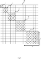
- Fig. 2 schematically shows a matrix chip 20 and is used to explain the binning function of the matrix chip 20.
- Binning is understood as the summarization of adjacent physical pixels already on the matrix chip 20 itself to a virtual pixel.
- a higher photosensitivity per virtual pixel can be achieved (for example, to improve the signal-to-noise ratio).
- the image resolution is reduced according to the number of combined pixels, making the image coarser.
- a lower image resolution has the advantage that the bandwidth can be reduced when transferring the data of a recording to a subsequent processing system.
- a smaller amount of data per shot also allows you to increase the frames per second (FPS).
- Fig. 2 now five different binning stages are shown as an example (the total number of pixels of the matrix chip 20 is purely schematic): starting from top left to bottom right no binning or a 1x1 binning 1, a 2x2 binning 2, a 3x3 binning 3, a 4x4 binning 4 and a 5x5 binning 5, where correspondingly 1, 4, 9, 16 and 25 physical pixels have been combined to form a virtual pixel.
- the physical pixels of the matrix chip 20 along a first direction, in particular along the direction of the web length y, along a second direction, in particular along the direction of the web width x or combined along the first direction and summarized in the second direction.
- the binning steps can be freely determined, such that the matrix sensor 20 can be designed, for example, to combine the pixels of the matrix chip 20 when using binning steps of the binning function, such that virtual pixels with a binning function Pixel size of 1x2, 1x3, 1x4, 1x5, 1x6, 1x7, 1x8, 1x9, 1x10, 1x11, 2x1, 3x1, 4x1, 5x1, 6x1, 7x1, 8x1, 9x1, 10x1, 11x1, 2x2, 3x2, 2x3, 4x2, 2x4, 5x2, 2x5, 6x2, 2x6, 7x2, 2x7, 8x2, 2x8, 9x2, 2x9, 10x2, 2x10, 11x2, 2x11, 3x3, 4x3, 3x4, 5x3, 3x5, 6x3, 3x6, 7x3, 3x7, 8x3, 3x8, 9x3, 3x9, 10x3, 3x10, 11x3, 3x11, 4x4, 5x4, 4x5, 6x4, 4x6,
- the distribution / number of combined pixels can be freely determined depending on the application and maximum physical resolution of the matrix chip 20 used, and is limited purely by the physical resolution of the matrix chip 20 used. This is to be regarded in particular with regard to the rapid advancement in the field of matrix sensors as well as the possible data transmission rates, so that the methods and devices described herein are by no means limited to the currently available matrix sensors / data rates.
- the method according to the invention uses the binning function of the matrix chip 20 in a new way and allows a physical zoom function without further complex devices such as additional movable cameras or zoom lenses. This is accomplished by the following procedure: making a first shot of a first portion of a web of material 10 at a first time with the camera 110 (comprising the matrix chip 20 with binning function) and making a second shot of a second portion of the web of material 10 to a second one Time with the camera 110.
- a first binning stage is used in which in each case a first number of pixels of the matrix chip 20 is combined using the binning function and for the second recording a second binning stage is used, wherein each of a second number of pixels of the matrix chip 20 is combined using the binning function.
- the first number of pixels combined each is higher or lower than the second number of pixels that are combined, thereby providing a physical zoom function for the second shot.
- a first example is the web observation, in which continuous recordings are observed with as constant a resolution as possible over the zoom levels.
- the zoom level used may be set, for example, or made according to an input of a user. That is, a user can specify the zoom level to be selected with which to take the pictures.
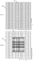
- Fig. 3A shows a time of a shot in which the full field of view (first active area 22) of the matrix chip 20 is used with a first binning step, for example to record a first portion of a web of material. If now a zoom recording is to be created, a reduced viewing area is recorded (with a second, smaller active area 24 of the matrix chip 20).
- a lower binning level is selected with the image resolution as constant as possible for the reduced viewing area (relative to the original viewing area), also means a larger number of pixels per mm for the reduced viewing area.
- This is schematically in Fig. 3B shown. It does not necessarily always have two consecutive shots have a different binning level. It may happen that a large number of recordings are made with the first binning stage, and the user is only provided with a second record with the second binning stage for certain events, for example because he has discovered an error. Also, after taking shots "zoomed in", the user may again be "zoomed out” to again observe a larger field of view of the matrix chip 20 and thus a larger portion of the web.
- the web 10 may, for example, have repeating patterns, e.g. in track observation per rapport a corresponding trigger signal is provided, so that the first time of the first recording of a first trigger signal can be determined and the second time of the second recording can be determined by a second trigger signal.
- control unit or a control unit can be used, which receives information from the sensor 140 for sending a trigger signal for the first recordings and the second recordings to the camera 110.
- the control unit or the control unit may be provided as an external device. But it is also possible that such a device or a control logic is installed directly in the camera 110.
- the sensor 140 may be connected directly to the controller or to the camera 110.
- a second example of the application of the device and method of the invention is inspection.
- second images are automatically created with the second binning stage in order to be able to inspect the defect in more detail.
- the first portion and the second portion may be two identical web portions or the second portion may be a portion of the first portion.
- a first active region 22 of the matrix chip 20 may be used for the first image in order to cover a first viewing region and for the second image a second active region 24 of the matrix chip 20 may be used to cover a second visual region.
- the first active area 22 and correspondingly the first viewing area may be larger than the second active area 24 and correspondingly the second viewing area.
- the second active area 24 may be the same size as the first active area 22 (see FIG Fig. 4A, 4B ).
- the second active region 24 may be part of the first active region 22, in particular within the first active region 22 (see FIG Fig.
- An advantage of this method is, for example, reducing the amount of data and the required computing power through the application of the binning function and a "region of interest" (ROI) function, since only the respectively required resolution or the respectively required field of view queried or recorded and is processed.
- ROI region of interest
- a reduced data load in turn also allows an increase in the image acquisition frequency (FPS).
- the viewing areas of the camera 110 or the matrix chip 20 may, for example, have a length and a width that are arranged according to the direction of the web length y and the direction of the web width x (the directions x and y are in the Fig. 2 to 6C shown).
- the viewing area is adjusted, the length and / or the width of the viewing area are changed.
- the principle of the "region of interest” (ROI) is used, in which it is exploited that it is possible to activate only certain areas 22, 24 of the sensor in the case of matrix chips 20: for the first recording, for example the entire field of view of the matrix sensor 20 (see Fig. 3A ) or a large part of the field of view become.
- a first binning stage is used, each of which combines relatively many physical pixels into a virtual pixel.
- a correspondingly selected second area 24 of the matrix chip 20 can be used to cover a second (smaller) field of view (an ROI is selected).
- a second binning stage is used, each of which combines relatively few physical pixels into a virtual pixel or completely breaks the binning (1x1 binning stage).
- the field of view can be the same for both shots (see, eg Fig. 4A, 4B ).
- a second binning stage is selected in which, compared to the first binning stage for the first recording, in each case only a smaller number of physical pixels is combined or no binning at all more is applied.
- the second shot would thus have a higher image resolution (number of pixels per mm) with the same size of field of view whereby the second shot would be displayed more accurate or, for example, a better physical resolution for a digital zoom function could be enabled.
- a digital zoom function in systems with two cameras and two lenses (eg a wide-angle lens and a Telephoto lens, so-called Dualview camera systems) a camera and a lens can be saved (an example below).
- FIGS. 3A and 3B to recognize which show an application of the method for a web observation, is here actually in the same ratio in X and Y direction from outside to inside (or from inside to outside) a correspondingly smaller 24 or larger area 22 is activated, depending on which Zoom level to which zoom level is to be changed.
- the drawings of the figures are to be understood here purely by way of example.
- Fig. 3A with respect to the matrix chip area in the x and y direction) of the matrix chip 20 is usually fully utilized in the web observation and only limited to an area 24 when zooming in.
- the resolution of 1024x768 pixels of the sensor remains constant over the optical zoom.
- the image resolution is 0.098 mm / pixel
- the minimum viewing area about 9 mm x 7 mm
- the image resolution is 0.009 mm / pixel. Thanks to the zoom lens, the constant resolution of 1024x768 pixels gives you a better image resolution in mm / pixel in the minimum field of view.
- the zoom lens is to be saved, but the claim is maintained that the quality of the images for the respective viewing areas is maintained.
- a binning stage with a 11x11 binning and a corresponding maximum viewing area of about 100 mm x 71 mm you get an image resolution of about 0.095 mm / virtual pixel. If you want to take a picture according to zoom level 12 of the 12x zoom lens, the binning function can be resolved (corresponds to the 1x1 binning level) and the field of view can be limited to approx. 9 mm x 7 mm.
- the image resolution is about 0.046 mm / pixel.
- the image resolution results only for the field of view through the sensor with wide-angle lens (first camera).
- digital zooming is performed, up to a field of view of e.g. 32mm x 24mm.
- second camera switch to the sensor with telephoto lens (second camera).
- digital zooming is again performed. That is, the resolution to the respective field of view is not kept constant, as in a track observation system with zoom lens.
- a camera and a lens are to be saved here, but again the claim is maintained that the quality of the images for the respective viewing areas is maintained.
- This can be achieved according to the invention, for example with a matrix chip with 70 megapixels (resolution for example 9735x7920).
- the matrix chip is binned for the maximum viewing area of 120 mm x 90 mm with binning stage 4x4, so that a physical resolution or virtual resolution (by combining physical pixels in the binning stage 4x4) of approximately 2434x1823 pixels is created, which approx. 0.049 mm / virtual pixel. From here on, theoretically, digital zooming could be achieved up to the viewing area of 32 mm x 24 mm become.
- the binning level would be set to 1x1 or binning would be completely resolved.
- the matrix chip then has an equivalent resolution of 2596 x 1944 pixels as the sensor of the second camera with a telephoto lens of the known system, which corresponds to approximately 0.012 mm / pixel. From here, digital zooming would be possible again, up to the visible range of min. 4mm x 3mm.
- the image resolution mm / pixel would then be in the field of view 120 mm x 90 mm to 32 mm x 24 mm, always at 0.049 mm / pixel and from 32 x 24 mm to 4 mm x 3 mm, even at 0.012 mm / pixel, since at smaller As the field of view also the resolution becomes smaller.
- the unused binning levels 3x3 and 2x2 could still be applied beyond a certain field of view in order to get better physical resolution values even earlier.
- the first shot for a user is displayed on a monitor, for example, and the second shot is made in response to user input, which is then also displayed to the user on the monitor, for example.
- the second binning stage and, optionally, the second viewing area can be selected depending on the user input. If a digital zoom is used, it can also be selected depending on the user input. That is, the number of pixels merged in the second binning stage (more or less than in the first binning stage for the first shot) and the position and size of the viewing area (ROI) may be user-controlled.
- the first active area 22 and the second active area 24 of the matrix chip 20 are not identical, may overlap or may not overlap. In addition, several trigger signals are output per repeat, since a 100% inspection of the web 10 takes place.
- the method then includes evaluating the first shot and determining a position of at least one flaw 26 on the web 10. Thereafter, the second binning step and / or the second active region 24 may be determined based on the location of the flaw 26.
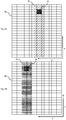
- FIGS. 4A and 4B show Example, with a first active area 22 in which the error 26 was detected (see Fig. 4A ). Fig.
- FIGS. 4A and 4B represent the matrix chip 20 for the second shot at the second time, in which the material web in the y-direction has run a bit further.
- the second active region 24 is now used in a smaller binning stage and thus with a higher resolution in order to be able to more accurately record and display the defect 26 and to be able to inspect it.
- the method is particularly advantageous in the inspection, if not only the binning stage for the second active region 24 is changed, as in FIGS. 4A and 4B but also the viewing range in the x and y direction can be limited to the position of the error. This is in Figs. 5A and 5B shown schematically.
- the binning function is resolved for at least one area of the matrix chip 20 or the binning level is reduced and, optionally, the ROI is selected by selecting the second active area 24 such that a viewing area of the camera for the second shot results a subsequent second recording of the error 26 or (several pictures of the error 26a, 26b, see FIGS. 6A to 6C ) with higher resolution, which can then be stored or displayed for a user, for example.
- the second shot may also be made at the second time based on the location of the error 26.
- the position of the error 26 may be determined, for example, in coordinates with respect to the direction of the web length y and the direction of the web width x. Based on these coordinates and the web speed of the web 10 (measured, for example, by the sensor 140), the second time for the second shot can then be determined.
- the second active region 24 can be determined as a function of a material web speed. For the second active region 24, its position in the direction of the material web length y, in the direction of the material web width x and / or a size based on the position of the defect 26 and the size of the defect 26 can be determined. This is an advantage because the second shot focuses specifically on the error range.
- the data load can be further reduced and the resolution increased, since only a small area of the matrix chip 20 with a reduced or resolved binning function has to be activated. That is, the first and second active regions 24 and the adaptation of the binning stage (or the complete resolution of the Binnings) can be variably adjusted.
- the image recording for the 100% inspection and the image recording of a visual display error it is also possible to take an image recording for a web observation.
- the principle according to the invention can also be used, for example, for a variable error classification, in which it is also possible to set the error variable to be recognized during operation even downwards (or also upwards).
- a variable error classification in which it is also possible to set the error variable to be recognized during operation even downwards (or also upwards).
- the resolution for the first active area 22 could be increased (if this gives the hardware) so that even smaller errors can be detected, which then in the second active area 24 by means of the second recording even higher resolution can be recorded.
- this is also possible in the other direction: if certain error quantities are tolerable, then the resolution for the first active region 22 can also be lowered. It can therefore be set directly on the resolution used for the first active area 22, from which error size the errors are recognizable. If an error is detected, it is then recorded in the second active area 24 by means of the second recording with a higher resolution.
- the apparatus may also include a web position sensor that determines, for example, a position or width of the web (in the x direction).
- the signals of the position sensor can be provided to the control unit, so that based thereon the active areas 22, 24 of the matrix sensor are determined, in particular a size and / or a position of the active areas 22, 24 can be set in the direction of the material web width x.
- the location of a plurality of errors 26a, 26b may be determined and a corresponding plurality of second recordings may be made. If the two or more errors 26a, 26b have the same position in the direction of the web length y, these two or more errors 26a, 26b can also be recorded simultaneously in a second recording with the correspondingly higher resolution.
- the matrix chip 20 is divided into first and second parts 20a, 20b, wherein the first part 20a works with the first binning stage and is used for the first recording and the second part 20b works with the second binning stage and for the second recording is used.
- the second part 20b lies in the direction of the web movement behind the first part 20a. It can then be provided, for example, that the second part 20b is activated only if an error 26a, 26b was found in the first image.
- the first part 20a may be larger than the second part 20b.
- the first part 20a may be at least twice as large, at least three times as large, at least five times as large, or at least nine times as large as the second part 20b.
- the first part 20a may occupy about 90% of the matrix chip 20 and the second part 20b may occupy about 10% of the matrix chip 20. It may also be advantageous to increase the camera parameter "Gain” for the second part 20b in order to compensate for a poorer light output in this less-fringed state or to reduce the image noise. Of course, this also applies to all other examples of application of the method according to the invention described herein.
- the camera parameter "Gain” can be increased or adjusted to a certain binning level in order to compensate for a possibly worse light output.
- first recordings with the first part 20a and second recordings with the second part 20b can be made continuously.
- the second recordings can be stored continuously in a ring buffer.
- Corresponding second recordings can be read from the ring buffer and / or made available to a user and / or displayed on a monitor, for example, if at least one error 26a, 26b has been detected in corresponding first recordings.
- Both the first recordings and the second recordings can cover 100% of the material web 10.
- the number of second receptacles must be adjusted according to the size ratios of the first and second parts 20a, 20b.
- the first part 20a occupies, for example, 90% of the matrix chip 20 and the second part 20b occupies 10% of the matrix chip 20
- a total of nine second receptacles with the second part 20b must be created for each first recording with the first part 20a ,
- the second part 20b has to be triggered nine times for nine shots while the first part 20a has to be triggered only once.
- the first part 20a has a binning level of 9x9 and the second part 20b has a binning level of 1x1 (that is, virtually no binning is used)
- this approach is advantageous because the individual data packets (the first and second recordings) always include an equivalent data size that can be tuned to an available bandwidth. The available bandwidth is then never exceeded.
- a suitable ratio of the parameters size ratio of the first part 20a to the second part 20b of the matrix chip 20 and used binning stage of the respective parts
- a suitable ratio of the parameters size ratio of the first part 20a to the second part 20b of the matrix chip 20 and used binning stage of the respective parts
- Fig. 6B show a recording with the second part 20b to one Time at which the first error 26a is in the field of view of the second part 20b.
- Fig. 6C shows a further recording with the second part 20b at a later time at which the second error 26b is in the field of view of the second part 20b.
- a further advantage of this method or device 100 is that it is also possible to display one-time errors in high-resolution, it does not necessarily have to be repetition errors.
- the ROI in the y direction and optionally also in the x direction
- the binning stage are adapted and the same error is recorded again in high resolution becomes.
- a digital zoom function in particular for example by interpolation of a plurality of adjacent physical pixels or virtual pixels which have arisen when using the binning function.
- the digital zoom feature can cover transition ranges in resolution between corresponding binning levels. This is advantageous in the method described herein, as the physical resolution can be adapted over and over again by the binning stages, so that degradation due to the use of the digital zoom is barely perceptible. In other words, even before an image looks blurred or pixellated by excessive digital zoom and interpolation (e.g., when displayed on a monitor), the next binning stage can be used, which again provides higher physical resolution.
- the digital zoom function can also be used after the binning stages have been completely resolved, ie the physical zoom function is exhausted.
- the selection of the binning stages as well as the areas to be activated are relatively freely determinable.
- the step zooming method it is possible to match the selected viewing areas and the binning steps so that, for each viewing area, for example, the same resolution (in terms of the total number of (virtual) pixels per viewing area) is given is. As a result, the size of the data packets sent per recording remains the same.
- the binning steps can also be adjusted so that the resolution is reduced in a constant field of view, for example, to increase the image acquisition frequency (FPS).
- FPS image acquisition frequency
- a resolution of 2048 x 1024 then 56 FPS can be sent to the control unit via a single Gigabit Ethernet interface.
- the resolution of 2048 x 512 is used (for example by 1x2 binning or by limiting the field of view)
- 112 FPS can be sent to the control unit via the Single Gigabit Ethernet Interface.
- the FPS and the viewing area again determine the maximum possible web speed for a 100% inspection of the material web 10.
- the respective active regions 22, 24 and thereby the respective viewing region and the binning stage to be used can be optimally matched to one another as a function of a maximum physical resolution of the matrix chip 20, the web speed and the properties of an objective 112 optionally used for the images become.
- the properties of the optionally used objective can also be adapted as a function of the maximum physical resolution of the matrix chip 20.
- the matrix chip 20 may have a resolution of at least 16 megapixels, at least 32 megapixels, at least 50 megapixels, at least 70 megapixels, or at least 100 megapixels.
- due to the rapid development in this area no limit can be seen up.
- an additional recording of the first section is produced at a third time using the first binning stage, wherein a different active area of the matrix chip 20 is used for the additional recording of the first section than for the first recording of the first section.
- the third time is after the first time.
- the third time is before the second time or after the second time, depending on the application.
- different types of illumination are used to illuminate the material web 10, so that one can create two different image sequences (with two different types of illumination) of the complete material web 10. For example, it may be illuminated once with illumination device 120 and once illuminated with illumination device 130.
- an additional recording of the second portion is created at a fourth time using the second binning stage, wherein for the additional recording of the second portion, another active area of the matrix chip 20 is used as for the first recording of the second section.
- the fourth time is after the second or after the third time.
- the same type of illumination can be used as for the additional reception of the first section, in particular a different type of illumination than for the second reception of the second section. This would mean, for example, in sum: continuously one shot each with first illumination and low resolution, first illumination and high resolution, second illumination and low resolution, and second illumination of high resolution.
- different types of illumination for illuminating the material web 10 can thus be used.
- the multi-inspection is not limited to two exposures per section with two illuminations.
- the device can also be used for a multi-inspection with three or more image sequences.
- further types of illumination can be used to illuminate the material web 10.
- the types of illumination may be selected from the group consisting of reflected light, backlight, and transmitted light.
- a range of lighting properties can be realized: homogeneous or inhomogeneous illumination, direct, diffuse, focused or collimated illumination, coaxial, transmissive and / or polarized illumination, different illumination angles and bright field or dark field illumination, light wavelengths in the UV, visible or IR range (um eg to be able to inspect security features), monochrome (monochrome), multicolored (polychrome) or color tunable or controllable (RGB) lighting, area lighting or line lighting, constant or flashed lighting, in incident and transmitted light illumination, these can be used alternately or simultaneously come.
- the lighting devices can be designed as a tunnel lighting system, tube lighting system or dome lighting system, as well as be modular or adapted to the web width.
- bulbs can be used, for example, incandescent lamps, gas discharge lamps, LED lighting, OLED lighting or laser lighting.
- LED lighting for example, the different types of lighting and properties can be used for the following multi-inspection: print-image inspection with visible incident light, label inspection with visible transmitted light and inspection of UV security features with UV incident light.
- image acquisition for web inspection can be carried out with the image sequence of the 100% inspection or the image of the 100% inspection can be output as image for web monitoring.
- the output image then corresponds to the resolution which was taken for the inspection. If an extra image recording of the web observation is made with the first and / or second illumination, again the viewing area and the image resolution can be adjusted accordingly and thus physically zoomed.
- the apparatus may also include a plurality of cameras 110, each having a matrix chip with binning function and ROI function, each of the cameras providing corresponding recordings for the web tracking and / or inspection methods described above.
- the cameras can be distributed over the material web width x, so that the viewing areas of the cameras adjoin or overlap one another in the direction of the material web width x.
- a coherent recording can be determined.
- mechanical offsets of the cameras in the direction of the material web length y relative to one another can be compensated by a corresponding selection of active regions of the matrix chips 20.
- the camera array can detect a continuous material web section positioned in the direction of the material web length y.
- At least one camera 110 can also be provided on the front side of the material web 10 and at least one camera on a rear side of the material web 10, wherein again each of the cameras corresponding receptacles for the previously described method of web observation and or Inspection can create. This allows the observation or inspection of both material web pages.
Landscapes
- Engineering & Computer Science (AREA)
- Physics & Mathematics (AREA)
- General Physics & Mathematics (AREA)
- Analytical Chemistry (AREA)
- General Health & Medical Sciences (AREA)
- Health & Medical Sciences (AREA)
- Life Sciences & Earth Sciences (AREA)
- Chemical & Material Sciences (AREA)
- Pathology (AREA)
- Biochemistry (AREA)
- Immunology (AREA)
- Signal Processing (AREA)
- Textile Engineering (AREA)
- Multimedia (AREA)
- Computer Vision & Pattern Recognition (AREA)
- Theoretical Computer Science (AREA)
- Quality & Reliability (AREA)
- Investigating Materials By The Use Of Optical Means Adapted For Particular Applications (AREA)
Applications Claiming Priority (1)
| Application Number | Priority Date | Filing Date | Title |
|---|---|---|---|
| DE102016220757.1A DE102016220757A1 (de) | 2016-10-21 | 2016-10-21 | Verfahren und Vorrichtung zur Materialbahnbeobachtung und Materialbahninspektion |
Publications (2)
| Publication Number | Publication Date |
|---|---|
| EP3312596A1 true EP3312596A1 (fr) | 2018-04-25 |
| EP3312596B1 EP3312596B1 (fr) | 2021-11-17 |
Family
ID=60083792
Family Applications (1)
| Application Number | Title | Priority Date | Filing Date |
|---|---|---|---|
| EP17195965.3A Active EP3312596B1 (fr) | 2016-10-21 | 2017-10-11 | Procédé et dispositif d'observation de bande de matériau et d'inspection de bande de matériau |
Country Status (6)
| Country | Link |
|---|---|
| US (1) | US10878552B2 (fr) |
| EP (1) | EP3312596B1 (fr) |
| JP (2) | JP7266362B2 (fr) |
| KR (1) | KR102416273B1 (fr) |
| CN (1) | CN107976450B (fr) |
| DE (1) | DE102016220757A1 (fr) |
Cited By (1)
| Publication number | Priority date | Publication date | Assignee | Title |
|---|---|---|---|---|
| CN111586289A (zh) * | 2020-03-31 | 2020-08-25 | 广东利元亨智能装备股份有限公司 | 一种高速飞拍控制方法及系统 |
Families Citing this family (15)
| Publication number | Priority date | Publication date | Assignee | Title |
|---|---|---|---|---|
| EP3502637A1 (fr) * | 2017-12-23 | 2019-06-26 | ABB Schweiz AG | Procédé et système de surveillance de fabrication de bandes en temps réel |
| JP6927124B2 (ja) | 2018-03-30 | 2021-08-25 | 東洋紡株式会社 | 熱収縮性ポリエステル系フィルム |
| JP2020000580A (ja) * | 2018-06-29 | 2020-01-09 | 株式会社三洋物産 | 遊技機 |
| JP2020000581A (ja) * | 2018-06-29 | 2020-01-09 | 株式会社三洋物産 | 遊技機 |
| JP2020000577A (ja) * | 2018-06-29 | 2020-01-09 | 株式会社三洋物産 | 遊技機 |
| JP2020000578A (ja) * | 2018-06-29 | 2020-01-09 | 株式会社三洋物産 | 遊技機 |
| EP3661191A1 (fr) * | 2018-11-27 | 2020-06-03 | B&R Industrial Automation GmbH | Procédé de lecture d'un capteur de superficie |
| KR102629343B1 (ko) * | 2018-12-21 | 2024-01-26 | 삼성전자주식회사 | 다중 셀 구조의 카메라 모듈 및 그 카메라 모듈을 포함하는 휴대용 통신 장치 |
| US20200371040A1 (en) * | 2019-05-21 | 2020-11-26 | Industrial Maintenance Engineering, Inc. d/b/a AIS Gauging | Static full width measurement system |
| US11218641B2 (en) * | 2019-09-09 | 2022-01-04 | Qualcomm Incorporated | Image capture mode adaptation |
| JP7552181B2 (ja) * | 2020-09-16 | 2024-09-18 | 東洋製罐グループホールディングス株式会社 | 表面検査システム |
| KR102580271B1 (ko) | 2021-02-25 | 2023-09-20 | 삼성전자주식회사 | 이미지센서를 이용한 다중 생체신호 측정 장치 및 방법과, 전자장치 |
| WO2024028811A1 (fr) * | 2022-08-05 | 2024-02-08 | Corephotonics Ltd. | Systèmes et procédés pour caméra numérique à zoom avec champ de vision à zoom réglable automatique |
| CN116109552A (zh) * | 2022-11-08 | 2023-05-12 | 中国计量大学 | 一种光纤缺陷检测方法和系统 |
| CN116718276A (zh) * | 2023-04-20 | 2023-09-08 | 中国人民解放军93236部队 | 一种基于f数和像元尺寸匹配重构的红外成像系统 |
Citations (7)
| Publication number | Priority date | Publication date | Assignee | Title |
|---|---|---|---|---|
| US20050226466A1 (en) * | 2004-04-06 | 2005-10-13 | Quad/Tech, Inc. | Image acquisition assembly |
| EP2003443A1 (fr) * | 2008-02-11 | 2008-12-17 | Texmag GmbH Vertriebsgesellschaft | Dispositif d'enregistrement d'une image |
| US20100214416A1 (en) * | 2006-02-01 | 2010-08-26 | Hannu Ruuska | Device for Monitoring a Web |
| US20110141269A1 (en) * | 2009-12-16 | 2011-06-16 | Stephen Michael Varga | Systems And Methods For Monitoring On-Line Webs Using Line Scan Cameras |
| US20120013733A1 (en) * | 2010-07-15 | 2012-01-19 | Eltromat Gmbh | Apparatus for Monitoring a Print Result in a Rotary Printing Press |
| WO2012049370A1 (fr) * | 2010-10-13 | 2012-04-19 | Metso Automation Oy | Système de suivi d'une feuille continue et procédé correspondant pour le suivi de la feuille continue |
| US20150077538A1 (en) * | 2012-02-17 | 2015-03-19 | Stephan Krebs | Apparatus and Method for Inspecting Printed Images |
Family Cites Families (23)
| Publication number | Priority date | Publication date | Assignee | Title |
|---|---|---|---|---|
| JPH0686183A (ja) * | 1992-08-31 | 1994-03-25 | Canon Inc | 固体撮像素子 |
| JPH11248641A (ja) * | 1998-03-03 | 1999-09-17 | Sumitomo Metal Ind Ltd | 表面欠陥検査装置及び表面欠陥検査方法 |
| AT406528B (de) * | 1998-05-05 | 2000-06-26 | Oesterr Forsch Seibersdorf | Verfahren und einrichtung zur feststellung, insbesondere zur visualisierung, von fehlern auf der oberfläche von gegenständen |
| SE523681C2 (sv) | 2002-04-05 | 2004-05-11 | Integrated Vision Prod | System och sensor för avbildning av egenskaper hos ett objekt |
| JP4151948B2 (ja) | 2002-11-07 | 2008-09-17 | 住友化学株式会社 | 帯状被検体の検査システム及び検査プログラム |
| US7257278B2 (en) | 2003-02-26 | 2007-08-14 | Hewlett-Packard Development Company, L.P. | Image sensor for capturing and filtering image data |
| US7688364B2 (en) * | 2004-12-10 | 2010-03-30 | Ambarella, Inc. | Decimating and cropping based zoom factor for a digital camera |
| JP4655991B2 (ja) | 2006-04-21 | 2011-03-23 | カシオ計算機株式会社 | 撮像装置及び電子ズーム方法と、プログラム |
| JP2008172506A (ja) | 2007-01-11 | 2008-07-24 | Nec Corp | イメージセンサ |
| DE102007055820A1 (de) * | 2007-12-14 | 2009-06-18 | Voith Patent Gmbh | Verfahren und Vorrichtung zur Erfassung zumindest einer die Eigenschaften einer Oberfläche in einer Materialbahnbehandlungseinrichtung wenigstens mittelbar charaktersierenden Größe und Verfahren zur Optimierung der Betriebsweise einer Materialbahnbehandlungseinrichtung |
| FR2936605B1 (fr) * | 2008-10-01 | 2014-10-31 | Saint Gobain | Dispositif d'analyse de la surface d'un substrat |
| DE102009029081A1 (de) * | 2009-09-02 | 2011-03-03 | Voith Patent Gmbh | Lasermarkierung |
| JP4813628B1 (ja) | 2010-03-23 | 2011-11-09 | 富士フイルム株式会社 | 撮影装置及びその制御方法、並びに三次元情報測定装置 |
| US20130208978A1 (en) * | 2010-10-19 | 2013-08-15 | 3M Innovative Properties Company | Continuous charting of non-uniformity severity for detecting variability in web-based materials |
| ES2793373T3 (es) * | 2010-12-30 | 2020-11-13 | Alltec Angewandte Laserlicht Tech Gesellschaft Mit Beschraenkter Haftung | Aparato sensor |
| JP5983616B2 (ja) | 2011-09-13 | 2016-09-06 | 日本電気株式会社 | 撮像装置、撮像方法及びプログラム |
| KR101205128B1 (ko) | 2012-05-11 | 2012-11-26 | 주식회사 앤비젼 | 이미지 센서 비닝 기법을 이용하여 이미지 센서의 픽셀당 해상도를 조정하는 광학 검사 장치 |
| CN102721702A (zh) * | 2012-06-27 | 2012-10-10 | 山东轻工业学院 | 基于嵌入式处理器的分布式纸病检测系统及方法 |
| WO2014188457A1 (fr) | 2013-05-23 | 2014-11-27 | Centro Sviluppo Materiali S.P.A. | Procédé d'inspection de surface de produits longs, et appareil convenant pour mettre en oeuvre un tel procédé |
| CN104422698B (zh) * | 2013-09-04 | 2017-03-29 | 昆山钞票纸业有限公司 | 随动式防伪纸定位施放荧光纤维在线检测装置 |
| JP2015105930A (ja) | 2013-12-02 | 2015-06-08 | 旭硝子株式会社 | 透光性基板の微小欠陥検査方法および透光性基板の微小欠陥検査装置 |
| CN104713483B (zh) * | 2015-03-30 | 2017-09-12 | 昆山钞票纸业有限公司 | 防伪纸内嵌光敏纤维的检测方法和装置 |
| CN105203557B (zh) * | 2015-10-28 | 2018-06-08 | 江西洁美电子信息材料有限公司 | 一种电子纸带造纸质量在线检测系统 |
-
2016
- 2016-10-21 DE DE102016220757.1A patent/DE102016220757A1/de active Pending
-
2017
- 2017-10-11 EP EP17195965.3A patent/EP3312596B1/fr active Active
- 2017-10-18 KR KR1020170135385A patent/KR102416273B1/ko active Active
- 2017-10-19 CN CN201710979576.0A patent/CN107976450B/zh active Active
- 2017-10-19 US US15/788,333 patent/US10878552B2/en active Active
- 2017-10-20 JP JP2017203346A patent/JP7266362B2/ja active Active
-
2022
- 2022-03-22 JP JP2022045740A patent/JP7311665B2/ja active Active
Patent Citations (7)
| Publication number | Priority date | Publication date | Assignee | Title |
|---|---|---|---|---|
| US20050226466A1 (en) * | 2004-04-06 | 2005-10-13 | Quad/Tech, Inc. | Image acquisition assembly |
| US20100214416A1 (en) * | 2006-02-01 | 2010-08-26 | Hannu Ruuska | Device for Monitoring a Web |
| EP2003443A1 (fr) * | 2008-02-11 | 2008-12-17 | Texmag GmbH Vertriebsgesellschaft | Dispositif d'enregistrement d'une image |
| US20110141269A1 (en) * | 2009-12-16 | 2011-06-16 | Stephen Michael Varga | Systems And Methods For Monitoring On-Line Webs Using Line Scan Cameras |
| US20120013733A1 (en) * | 2010-07-15 | 2012-01-19 | Eltromat Gmbh | Apparatus for Monitoring a Print Result in a Rotary Printing Press |
| WO2012049370A1 (fr) * | 2010-10-13 | 2012-04-19 | Metso Automation Oy | Système de suivi d'une feuille continue et procédé correspondant pour le suivi de la feuille continue |
| US20150077538A1 (en) * | 2012-02-17 | 2015-03-19 | Stephan Krebs | Apparatus and Method for Inspecting Printed Images |
Cited By (1)
| Publication number | Priority date | Publication date | Assignee | Title |
|---|---|---|---|---|
| CN111586289A (zh) * | 2020-03-31 | 2020-08-25 | 广东利元亨智能装备股份有限公司 | 一种高速飞拍控制方法及系统 |
Also Published As
| Publication number | Publication date |
|---|---|
| KR102416273B1 (ko) | 2022-07-05 |
| JP2018066740A (ja) | 2018-04-26 |
| JP7311665B2 (ja) | 2023-07-19 |
| CN107976450A (zh) | 2018-05-01 |
| JP7266362B2 (ja) | 2023-04-28 |
| JP2022091853A (ja) | 2022-06-21 |
| US20180114308A1 (en) | 2018-04-26 |
| KR20180044198A (ko) | 2018-05-02 |
| CN107976450B (zh) | 2021-10-29 |
| US10878552B2 (en) | 2020-12-29 |
| EP3312596B1 (fr) | 2021-11-17 |
| DE102016220757A1 (de) | 2018-04-26 |
Similar Documents
| Publication | Publication Date | Title |
|---|---|---|
| EP3312596B1 (fr) | Procédé et dispositif d'observation de bande de matériau et d'inspection de bande de matériau | |
| DE102008018225B4 (de) | Optischer Navigationsschaltkreis einer optischen Maus, dynamisches Rekonfigurationsverfahren für ein Pixelarray sowie Vorrichtung | |
| EP3729137B1 (fr) | Système lidar à impulsions multiples pour la détection multidimensionnelle d'objets | |
| DE102008034979B4 (de) | Verfahren und Einrichtung zur Erzeugung von fehlerreduzierten hochauflösenden und kontrastverbesserten Bildern | |
| DE112008003337B4 (de) | Eigenschaftsanalysegerät | |
| EP1610270A2 (fr) | Procédé d'évaluation d'un materiel avec au moins une caractéristique d'identification | |
| DE60302946T2 (de) | Bildsegmentierungsverfahren und -vorrichtung zur MRC-basierten Darstellung von Dokumenten | |
| EP3291172B1 (fr) | Procédé de détermination de données d'image de résultat | |
| DE102009043747A1 (de) | Verfahren zur Erzeugung eines Mikroskopbildes und Mikroskop | |
| WO2019086686A1 (fr) | Réduction de perturbations d'image dans des images | |
| DE102014008686B4 (de) | Verfahren und Vorrichtung zur Farbinterpolation | |
| DE102022108603A1 (de) | Bildprüfvorrichtung und Bildprüfverfahren | |
| EP1585059A2 (fr) | Procédé et dispositif d'évaluation de vecteurs de vitesse attribués à des régions d'image | |
| DE102020109997A1 (de) | System und Verfahren, um zuverlässige gestitchte Bilder zu machen | |
| DE102009059977A1 (de) | Endoskopsystem mit Abtastfunktion | |
| EP1542051A1 (fr) | Procédé et système pour séparer des longueurs d'onde dans un microscope à balayage | |
| DE102010007730A1 (de) | Verfahren und Vorrichtung zum Einstellen eines geeigneten Auswerteparameters für ein Fluoreszenzmikroskop | |
| WO2024017675A1 (fr) | Système de caméra et procédé de fonctionnement correspondant | |
| WO2012084531A1 (fr) | Caméra munie d'un capteur d'image en couleur et procédé d'enregistrement avec une telle caméra | |
| DE112014006356B4 (de) | Verfahren zur Verbesserung der Bildqualität eines Ladungsträgerteilchen-Rastermikroskops und Ladungsträgerteilchen-Rastermikroskop | |
| EP3988989B1 (fr) | Procédé et microscope doté d'un dispositif de détection des déplacements d'un échantillon par rapport à une lentille | |
| DE102021130505B4 (de) | Verfahren zur Bestimmung einer Beleuchtungsfarbe, Bildverarbeitungsvorrichtung und Aufnahmesystem | |
| DE102020105984A1 (de) | Steuerungssystem für ein Mikroskop, Mikroskopanordnung und Verfahren zur bildgebenden Positionierungsunterstützung | |
| EP1729258A2 (fr) | Procédé et dispositif destinés à la détermination de vecteurs de déplacement | |
| EP4045931A1 (fr) | Système lidar à impulsions multiples et procédé de capture d'un objet dans une région observée |
Legal Events
| Date | Code | Title | Description |
|---|---|---|---|
| PUAI | Public reference made under article 153(3) epc to a published international application that has entered the european phase |
Free format text: ORIGINAL CODE: 0009012 |
|
| STAA | Information on the status of an ep patent application or granted ep patent |
Free format text: STATUS: EXAMINATION IS IN PROGRESS |
|
| 17P | Request for examination filed |
Effective date: 20171011 |
|
| AK | Designated contracting states |
Kind code of ref document: A1 Designated state(s): AL AT BE BG CH CY CZ DE DK EE ES FI FR GB GR HR HU IE IS IT LI LT LU LV MC MK MT NL NO PL PT RO RS SE SI SK SM TR |
|
| AX | Request for extension of the european patent |
Extension state: BA ME |
|
| GRAP | Despatch of communication of intention to grant a patent |
Free format text: ORIGINAL CODE: EPIDOSNIGR1 |
|
| STAA | Information on the status of an ep patent application or granted ep patent |
Free format text: STATUS: GRANT OF PATENT IS INTENDED |
|
| INTG | Intention to grant announced |
Effective date: 20210104 |
|
| GRAJ | Information related to disapproval of communication of intention to grant by the applicant or resumption of examination proceedings by the epo deleted |
Free format text: ORIGINAL CODE: EPIDOSDIGR1 |
|
| STAA | Information on the status of an ep patent application or granted ep patent |
Free format text: STATUS: EXAMINATION IS IN PROGRESS |
|
| INTC | Intention to grant announced (deleted) | ||
| GRAS | Grant fee paid |
Free format text: ORIGINAL CODE: EPIDOSNIGR3 |
|
| STAA | Information on the status of an ep patent application or granted ep patent |
Free format text: STATUS: GRANT OF PATENT IS INTENDED |
|
| GRAP | Despatch of communication of intention to grant a patent |
Free format text: ORIGINAL CODE: EPIDOSNIGR1 |
|
| INTG | Intention to grant announced |
Effective date: 20210630 |
|
| RIN1 | Information on inventor provided before grant (corrected) |
Inventor name: HERRMANN, MARKUS Inventor name: KROEHN, MANFRED |
|
| GRAA | (expected) grant |
Free format text: ORIGINAL CODE: 0009210 |
|
| STAA | Information on the status of an ep patent application or granted ep patent |
Free format text: STATUS: THE PATENT HAS BEEN GRANTED |
|
| AK | Designated contracting states |
Kind code of ref document: B1 Designated state(s): AL AT BE BG CH CY CZ DE DK EE ES FI FR GB GR HR HU IE IS IT LI LT LU LV MC MK MT NL NO PL PT RO RS SE SI SK SM TR |
|
| REG | Reference to a national code |
Ref country code: GB Ref legal event code: FG4D Free format text: NOT ENGLISH |
|
| REG | Reference to a national code |
Ref country code: DE Ref legal event code: R096 Ref document number: 502017012032 Country of ref document: DE |
|
| REG | Reference to a national code |
Ref country code: IE Ref legal event code: FG4D Free format text: LANGUAGE OF EP DOCUMENT: GERMAN |
|
| REG | Reference to a national code |
Ref country code: AT Ref legal event code: REF Ref document number: 1448446 Country of ref document: AT Kind code of ref document: T Effective date: 20211215 |
|
| REG | Reference to a national code |
Ref country code: LT Ref legal event code: MG9D |
|
| REG | Reference to a national code |
Ref country code: NL Ref legal event code: MP Effective date: 20211117 |
|
| PG25 | Lapsed in a contracting state [announced via postgrant information from national office to epo] |
Ref country code: RS Free format text: LAPSE BECAUSE OF FAILURE TO SUBMIT A TRANSLATION OF THE DESCRIPTION OR TO PAY THE FEE WITHIN THE PRESCRIBED TIME-LIMIT Effective date: 20211117 Ref country code: LT Free format text: LAPSE BECAUSE OF FAILURE TO SUBMIT A TRANSLATION OF THE DESCRIPTION OR TO PAY THE FEE WITHIN THE PRESCRIBED TIME-LIMIT Effective date: 20211117 Ref country code: FI Free format text: LAPSE BECAUSE OF FAILURE TO SUBMIT A TRANSLATION OF THE DESCRIPTION OR TO PAY THE FEE WITHIN THE PRESCRIBED TIME-LIMIT Effective date: 20211117 Ref country code: BG Free format text: LAPSE BECAUSE OF FAILURE TO SUBMIT A TRANSLATION OF THE DESCRIPTION OR TO PAY THE FEE WITHIN THE PRESCRIBED TIME-LIMIT Effective date: 20220217 |
|
| PG25 | Lapsed in a contracting state [announced via postgrant information from national office to epo] |
Ref country code: IS Free format text: LAPSE BECAUSE OF FAILURE TO SUBMIT A TRANSLATION OF THE DESCRIPTION OR TO PAY THE FEE WITHIN THE PRESCRIBED TIME-LIMIT Effective date: 20220317 Ref country code: SE Free format text: LAPSE BECAUSE OF FAILURE TO SUBMIT A TRANSLATION OF THE DESCRIPTION OR TO PAY THE FEE WITHIN THE PRESCRIBED TIME-LIMIT Effective date: 20211117 Ref country code: PT Free format text: LAPSE BECAUSE OF FAILURE TO SUBMIT A TRANSLATION OF THE DESCRIPTION OR TO PAY THE FEE WITHIN THE PRESCRIBED TIME-LIMIT Effective date: 20220317 Ref country code: PL Free format text: LAPSE BECAUSE OF FAILURE TO SUBMIT A TRANSLATION OF THE DESCRIPTION OR TO PAY THE FEE WITHIN THE PRESCRIBED TIME-LIMIT Effective date: 20211117 Ref country code: NO Free format text: LAPSE BECAUSE OF FAILURE TO SUBMIT A TRANSLATION OF THE DESCRIPTION OR TO PAY THE FEE WITHIN THE PRESCRIBED TIME-LIMIT Effective date: 20220217 Ref country code: NL Free format text: LAPSE BECAUSE OF FAILURE TO SUBMIT A TRANSLATION OF THE DESCRIPTION OR TO PAY THE FEE WITHIN THE PRESCRIBED TIME-LIMIT Effective date: 20211117 Ref country code: LV Free format text: LAPSE BECAUSE OF FAILURE TO SUBMIT A TRANSLATION OF THE DESCRIPTION OR TO PAY THE FEE WITHIN THE PRESCRIBED TIME-LIMIT Effective date: 20211117 Ref country code: HR Free format text: LAPSE BECAUSE OF FAILURE TO SUBMIT A TRANSLATION OF THE DESCRIPTION OR TO PAY THE FEE WITHIN THE PRESCRIBED TIME-LIMIT Effective date: 20211117 Ref country code: GR Free format text: LAPSE BECAUSE OF FAILURE TO SUBMIT A TRANSLATION OF THE DESCRIPTION OR TO PAY THE FEE WITHIN THE PRESCRIBED TIME-LIMIT Effective date: 20220218 Ref country code: ES Free format text: LAPSE BECAUSE OF FAILURE TO SUBMIT A TRANSLATION OF THE DESCRIPTION OR TO PAY THE FEE WITHIN THE PRESCRIBED TIME-LIMIT Effective date: 20211117 |
|
| PG25 | Lapsed in a contracting state [announced via postgrant information from national office to epo] |
Ref country code: SM Free format text: LAPSE BECAUSE OF FAILURE TO SUBMIT A TRANSLATION OF THE DESCRIPTION OR TO PAY THE FEE WITHIN THE PRESCRIBED TIME-LIMIT Effective date: 20211117 Ref country code: SK Free format text: LAPSE BECAUSE OF FAILURE TO SUBMIT A TRANSLATION OF THE DESCRIPTION OR TO PAY THE FEE WITHIN THE PRESCRIBED TIME-LIMIT Effective date: 20211117 Ref country code: RO Free format text: LAPSE BECAUSE OF FAILURE TO SUBMIT A TRANSLATION OF THE DESCRIPTION OR TO PAY THE FEE WITHIN THE PRESCRIBED TIME-LIMIT Effective date: 20211117 Ref country code: EE Free format text: LAPSE BECAUSE OF FAILURE TO SUBMIT A TRANSLATION OF THE DESCRIPTION OR TO PAY THE FEE WITHIN THE PRESCRIBED TIME-LIMIT Effective date: 20211117 Ref country code: DK Free format text: LAPSE BECAUSE OF FAILURE TO SUBMIT A TRANSLATION OF THE DESCRIPTION OR TO PAY THE FEE WITHIN THE PRESCRIBED TIME-LIMIT Effective date: 20211117 Ref country code: CZ Free format text: LAPSE BECAUSE OF FAILURE TO SUBMIT A TRANSLATION OF THE DESCRIPTION OR TO PAY THE FEE WITHIN THE PRESCRIBED TIME-LIMIT Effective date: 20211117 |
|
| REG | Reference to a national code |
Ref country code: DE Ref legal event code: R026 Ref document number: 502017012032 Country of ref document: DE |
|
| PLBI | Opposition filed |
Free format text: ORIGINAL CODE: 0009260 |
|
| PLAB | Opposition data, opponent's data or that of the opponent's representative modified |
Free format text: ORIGINAL CODE: 0009299OPPO |
|
| PLAX | Notice of opposition and request to file observation + time limit sent |
Free format text: ORIGINAL CODE: EPIDOSNOBS2 |
|
| 26 | Opposition filed |
Opponent name: BST GMBH Effective date: 20220811 |
|
| R26 | Opposition filed (corrected) |
Opponent name: BST GMBH Effective date: 20220811 |
|
| PG25 | Lapsed in a contracting state [announced via postgrant information from national office to epo] |
Ref country code: AL Free format text: LAPSE BECAUSE OF FAILURE TO SUBMIT A TRANSLATION OF THE DESCRIPTION OR TO PAY THE FEE WITHIN THE PRESCRIBED TIME-LIMIT Effective date: 20211117 |
|
| PG25 | Lapsed in a contracting state [announced via postgrant information from national office to epo] |
Ref country code: SI Free format text: LAPSE BECAUSE OF FAILURE TO SUBMIT A TRANSLATION OF THE DESCRIPTION OR TO PAY THE FEE WITHIN THE PRESCRIBED TIME-LIMIT Effective date: 20211117 |
|
| PLBB | Reply of patent proprietor to notice(s) of opposition received |
Free format text: ORIGINAL CODE: EPIDOSNOBS3 |
|
| PG25 | Lapsed in a contracting state [announced via postgrant information from national office to epo] |
Ref country code: MC Free format text: LAPSE BECAUSE OF FAILURE TO SUBMIT A TRANSLATION OF THE DESCRIPTION OR TO PAY THE FEE WITHIN THE PRESCRIBED TIME-LIMIT Effective date: 20211117 |
|
| REG | Reference to a national code |
Ref country code: CH Ref legal event code: PL |
|
| REG | Reference to a national code |
Ref country code: BE Ref legal event code: MM Effective date: 20221031 |
|
| GBPC | Gb: european patent ceased through non-payment of renewal fee |
Effective date: 20221011 |
|
| PG25 | Lapsed in a contracting state [announced via postgrant information from national office to epo] |
Ref country code: LU Free format text: LAPSE BECAUSE OF NON-PAYMENT OF DUE FEES Effective date: 20221011 |
|
| PG25 | Lapsed in a contracting state [announced via postgrant information from national office to epo] |
Ref country code: LI Free format text: LAPSE BECAUSE OF NON-PAYMENT OF DUE FEES Effective date: 20221031 Ref country code: CH Free format text: LAPSE BECAUSE OF NON-PAYMENT OF DUE FEES Effective date: 20221031 |
|
| PG25 | Lapsed in a contracting state [announced via postgrant information from national office to epo] |
Ref country code: BE Free format text: LAPSE BECAUSE OF NON-PAYMENT OF DUE FEES Effective date: 20221031 |
|
| PLCK | Communication despatched that opposition was rejected |
Free format text: ORIGINAL CODE: EPIDOSNREJ1 |
|
| PG25 | Lapsed in a contracting state [announced via postgrant information from national office to epo] |
Ref country code: IE Free format text: LAPSE BECAUSE OF NON-PAYMENT OF DUE FEES Effective date: 20221011 Ref country code: GB Free format text: LAPSE BECAUSE OF NON-PAYMENT OF DUE FEES Effective date: 20221011 |
|
| REG | Reference to a national code |
Ref country code: DE Ref legal event code: R100 Ref document number: 502017012032 Country of ref document: DE |
|
| REG | Reference to a national code |
Ref country code: AT Ref legal event code: MM01 Ref document number: 1448446 Country of ref document: AT Kind code of ref document: T Effective date: 20221011 |
|
| PG25 | Lapsed in a contracting state [announced via postgrant information from national office to epo] |
Ref country code: AT Free format text: LAPSE BECAUSE OF NON-PAYMENT OF DUE FEES Effective date: 20221011 |
|
| PLBN | Opposition rejected |
Free format text: ORIGINAL CODE: 0009273 |
|
| STAA | Information on the status of an ep patent application or granted ep patent |
Free format text: STATUS: OPPOSITION REJECTED |
|
| 27O | Opposition rejected |
Effective date: 20231103 |
|
| PG25 | Lapsed in a contracting state [announced via postgrant information from national office to epo] |
Ref country code: HU Free format text: LAPSE BECAUSE OF FAILURE TO SUBMIT A TRANSLATION OF THE DESCRIPTION OR TO PAY THE FEE WITHIN THE PRESCRIBED TIME-LIMIT; INVALID AB INITIO Effective date: 20171011 |
|
| PG25 | Lapsed in a contracting state [announced via postgrant information from national office to epo] |
Ref country code: CY Free format text: LAPSE BECAUSE OF FAILURE TO SUBMIT A TRANSLATION OF THE DESCRIPTION OR TO PAY THE FEE WITHIN THE PRESCRIBED TIME-LIMIT Effective date: 20211117 |
|
| PG25 | Lapsed in a contracting state [announced via postgrant information from national office to epo] |
Ref country code: MK Free format text: LAPSE BECAUSE OF FAILURE TO SUBMIT A TRANSLATION OF THE DESCRIPTION OR TO PAY THE FEE WITHIN THE PRESCRIBED TIME-LIMIT Effective date: 20211117 |
|
| PG25 | Lapsed in a contracting state [announced via postgrant information from national office to epo] |
Ref country code: MT Free format text: LAPSE BECAUSE OF FAILURE TO SUBMIT A TRANSLATION OF THE DESCRIPTION OR TO PAY THE FEE WITHIN THE PRESCRIBED TIME-LIMIT Effective date: 20211117 |
|
| PGFP | Annual fee paid to national office [announced via postgrant information from national office to epo] |
Ref country code: IT Payment date: 20250922 Year of fee payment: 9 |
|
| PGFP | Annual fee paid to national office [announced via postgrant information from national office to epo] |
Ref country code: FR Payment date: 20250908 Year of fee payment: 9 |
|
| PGFP | Annual fee paid to national office [announced via postgrant information from national office to epo] |
Ref country code: DE Payment date: 20250910 Year of fee payment: 9 |
|
| PGFP | Annual fee paid to national office [announced via postgrant information from national office to epo] |
Ref country code: TR Payment date: 20251003 Year of fee payment: 9 |