EP3330759B1 - Coupleur de lumière à circuit photonique et procédé associé - Google Patents
Coupleur de lumière à circuit photonique et procédé associé Download PDFInfo
- Publication number
- EP3330759B1 EP3330759B1 EP16202279.2A EP16202279A EP3330759B1 EP 3330759 B1 EP3330759 B1 EP 3330759B1 EP 16202279 A EP16202279 A EP 16202279A EP 3330759 B1 EP3330759 B1 EP 3330759B1
- Authority
- EP
- European Patent Office
- Prior art keywords
- waveguide
- integrated
- integrated waveguide
- layer
- cavity
- Prior art date
- Legal status (The legal status is an assumption and is not a legal conclusion. Google has not performed a legal analysis and makes no representation as to the accuracy of the status listed.)
- Active
Links
Images

Classifications
-
- G—PHYSICS
- G02—OPTICS
- G02B—OPTICAL ELEMENTS, SYSTEMS OR APPARATUS
- G02B6/00—Light guides; Structural details of arrangements comprising light guides and other optical elements, e.g. couplings
- G02B6/24—Coupling light guides
- G02B6/42—Coupling light guides with opto-electronic elements
- G02B6/4201—Packages, e.g. shape, construction, internal or external details
- G02B6/4204—Packages, e.g. shape, construction, internal or external details the coupling comprising intermediate optical elements, e.g. lenses, holograms
- G02B6/4214—Packages, e.g. shape, construction, internal or external details the coupling comprising intermediate optical elements, e.g. lenses, holograms the intermediate optical element having redirecting reflective means, e.g. mirrors, prisms for deflecting the radiation from horizontal to down- or upward direction toward a device
-
- G—PHYSICS
- G01—MEASURING; TESTING
- G01J—MEASUREMENT OF INTENSITY, VELOCITY, SPECTRAL CONTENT, POLARISATION, PHASE OR PULSE CHARACTERISTICS OF INFRARED, VISIBLE OR ULTRAVIOLET LIGHT; COLORIMETRY; RADIATION PYROMETRY
- G01J3/00—Spectrometry; Spectrophotometry; Monochromators; Measuring colours
- G01J3/02—Details
- G01J3/0205—Optical elements not provided otherwise, e.g. optical manifolds, diffusers, windows
- G01J3/021—Optical elements not provided otherwise, e.g. optical manifolds, diffusers, windows using plane or convex mirrors, parallel phase plates, or particular reflectors
-
- G—PHYSICS
- G01—MEASURING; TESTING
- G01J—MEASUREMENT OF INTENSITY, VELOCITY, SPECTRAL CONTENT, POLARISATION, PHASE OR PULSE CHARACTERISTICS OF INFRARED, VISIBLE OR ULTRAVIOLET LIGHT; COLORIMETRY; RADIATION PYROMETRY
- G01J3/00—Spectrometry; Spectrophotometry; Monochromators; Measuring colours
- G01J3/02—Details
- G01J3/0205—Optical elements not provided otherwise, e.g. optical manifolds, diffusers, windows
- G01J3/0218—Optical elements not provided otherwise, e.g. optical manifolds, diffusers, windows using optical fibers
-
- G—PHYSICS
- G01—MEASURING; TESTING
- G01J—MEASUREMENT OF INTENSITY, VELOCITY, SPECTRAL CONTENT, POLARISATION, PHASE OR PULSE CHARACTERISTICS OF INFRARED, VISIBLE OR ULTRAVIOLET LIGHT; COLORIMETRY; RADIATION PYROMETRY
- G01J3/00—Spectrometry; Spectrophotometry; Monochromators; Measuring colours
- G01J3/02—Details
- G01J3/0256—Compact construction
-
- G—PHYSICS
- G01—MEASURING; TESTING
- G01J—MEASUREMENT OF INTENSITY, VELOCITY, SPECTRAL CONTENT, POLARISATION, PHASE OR PULSE CHARACTERISTICS OF INFRARED, VISIBLE OR ULTRAVIOLET LIGHT; COLORIMETRY; RADIATION PYROMETRY
- G01J3/00—Spectrometry; Spectrophotometry; Monochromators; Measuring colours
- G01J3/02—Details
- G01J3/0256—Compact construction
- G01J3/0259—Monolithic
-
- G—PHYSICS
- G01—MEASURING; TESTING
- G01J—MEASUREMENT OF INTENSITY, VELOCITY, SPECTRAL CONTENT, POLARISATION, PHASE OR PULSE CHARACTERISTICS OF INFRARED, VISIBLE OR ULTRAVIOLET LIGHT; COLORIMETRY; RADIATION PYROMETRY
- G01J3/00—Spectrometry; Spectrophotometry; Monochromators; Measuring colours
- G01J3/12—Generating the spectrum; Monochromators
- G01J3/18—Generating the spectrum; Monochromators using diffraction elements, e.g. grating
- G01J3/1895—Generating the spectrum; Monochromators using diffraction elements, e.g. grating using fiber Bragg gratings or gratings integrated in a waveguide
-
- G—PHYSICS
- G01—MEASURING; TESTING
- G01J—MEASUREMENT OF INTENSITY, VELOCITY, SPECTRAL CONTENT, POLARISATION, PHASE OR PULSE CHARACTERISTICS OF INFRARED, VISIBLE OR ULTRAVIOLET LIGHT; COLORIMETRY; RADIATION PYROMETRY
- G01J3/00—Spectrometry; Spectrophotometry; Monochromators; Measuring colours
- G01J3/28—Investigating the spectrum
- G01J3/2803—Investigating the spectrum using photoelectric array detector
-
- G—PHYSICS
- G01—MEASURING; TESTING
- G01J—MEASUREMENT OF INTENSITY, VELOCITY, SPECTRAL CONTENT, POLARISATION, PHASE OR PULSE CHARACTERISTICS OF INFRARED, VISIBLE OR ULTRAVIOLET LIGHT; COLORIMETRY; RADIATION PYROMETRY
- G01J3/00—Spectrometry; Spectrophotometry; Monochromators; Measuring colours
- G01J3/28—Investigating the spectrum
- G01J3/2823—Imaging spectrometer
-
- G—PHYSICS
- G02—OPTICS
- G02B—OPTICAL ELEMENTS, SYSTEMS OR APPARATUS
- G02B6/00—Light guides; Structural details of arrangements comprising light guides and other optical elements, e.g. couplings
- G02B6/10—Light guides; Structural details of arrangements comprising light guides and other optical elements, e.g. couplings of the optical waveguide type
- G02B6/12—Light guides; Structural details of arrangements comprising light guides and other optical elements, e.g. couplings of the optical waveguide type of the integrated circuit kind
-
- G—PHYSICS
- G02—OPTICS
- G02B—OPTICAL ELEMENTS, SYSTEMS OR APPARATUS
- G02B6/00—Light guides; Structural details of arrangements comprising light guides and other optical elements, e.g. couplings
- G02B6/10—Light guides; Structural details of arrangements comprising light guides and other optical elements, e.g. couplings of the optical waveguide type
- G02B6/12—Light guides; Structural details of arrangements comprising light guides and other optical elements, e.g. couplings of the optical waveguide type of the integrated circuit kind
- G02B6/12007—Light guides; Structural details of arrangements comprising light guides and other optical elements, e.g. couplings of the optical waveguide type of the integrated circuit kind forming wavelength selective elements, e.g. multiplexer, demultiplexer
-
- G—PHYSICS
- G02—OPTICS
- G02B—OPTICAL ELEMENTS, SYSTEMS OR APPARATUS
- G02B6/00—Light guides; Structural details of arrangements comprising light guides and other optical elements, e.g. couplings
- G02B6/10—Light guides; Structural details of arrangements comprising light guides and other optical elements, e.g. couplings of the optical waveguide type
- G02B6/12—Light guides; Structural details of arrangements comprising light guides and other optical elements, e.g. couplings of the optical waveguide type of the integrated circuit kind
- G02B6/122—Basic optical elements, e.g. light-guiding paths
- G02B6/1228—Tapered waveguides, e.g. integrated spot-size transformers
-
- G—PHYSICS
- G02—OPTICS
- G02B—OPTICAL ELEMENTS, SYSTEMS OR APPARATUS
- G02B6/00—Light guides; Structural details of arrangements comprising light guides and other optical elements, e.g. couplings
- G02B6/10—Light guides; Structural details of arrangements comprising light guides and other optical elements, e.g. couplings of the optical waveguide type
- G02B6/12—Light guides; Structural details of arrangements comprising light guides and other optical elements, e.g. couplings of the optical waveguide type of the integrated circuit kind
- G02B6/13—Integrated optical circuits characterised by the manufacturing method
-
- G—PHYSICS
- G02—OPTICS
- G02B—OPTICAL ELEMENTS, SYSTEMS OR APPARATUS
- G02B6/00—Light guides; Structural details of arrangements comprising light guides and other optical elements, e.g. couplings
- G02B6/24—Coupling light guides
- G02B6/42—Coupling light guides with opto-electronic elements
- G02B6/4201—Packages, e.g. shape, construction, internal or external details
- G02B6/4249—Packages, e.g. shape, construction, internal or external details comprising arrays of active devices and fibres
- G02B6/425—Optical features
-
- G—PHYSICS
- G01—MEASURING; TESTING
- G01J—MEASUREMENT OF INTENSITY, VELOCITY, SPECTRAL CONTENT, POLARISATION, PHASE OR PULSE CHARACTERISTICS OF INFRARED, VISIBLE OR ULTRAVIOLET LIGHT; COLORIMETRY; RADIATION PYROMETRY
- G01J3/00—Spectrometry; Spectrophotometry; Monochromators; Measuring colours
- G01J3/28—Investigating the spectrum
- G01J3/2803—Investigating the spectrum using photoelectric array detector
- G01J2003/2813—2D-array
-
- G—PHYSICS
- G02—OPTICS
- G02B—OPTICAL ELEMENTS, SYSTEMS OR APPARATUS
- G02B6/00—Light guides; Structural details of arrangements comprising light guides and other optical elements, e.g. couplings
- G02B6/10—Light guides; Structural details of arrangements comprising light guides and other optical elements, e.g. couplings of the optical waveguide type
- G02B6/12—Light guides; Structural details of arrangements comprising light guides and other optical elements, e.g. couplings of the optical waveguide type of the integrated circuit kind
- G02B2006/12133—Functions
- G02B2006/12147—Coupler
Definitions
- the invention relates to the field of photonic integrated circuit devices. More specifically it relates to an integrated photonic device in which a light signal is coupled from an integrated waveguide to a planar detector comprising at least one photodetector, such as an image detector, and methods related thereto.
- a photonic circuit may be provided on an image detector.
- a plurality of grating couplers may couple light from a waveguide towards an image detector for detection.
- US 6,226,083 discloses an integrated-optic spectrometer for analysing the composition of light reflected off a sample under analysis.
- the integrated-optic spectrometer comprises a waveguide, fabricated onto an oxidized substrate, and an array of diffraction gratings and a detector array.
- the detector array is mounted on the waveguide to receive the light of different wavelengths diffracted by the grating array, e.g. such as to enable the analysis of different discrete wavelengths.
- the diffraction gratings each comprise a series of grating lines and are constructed to provide optimal transmission of wavelengths not diffracted by the diffraction grating.
- the input light is guided through the waveguide and discrete wavelengths are diffracted by the diffraction gratings onto the photodiode detector array which in turn measures the intensity of the light at the discrete wavelengths for determining composition, while optimally transmitting non-diffracted wavelengths through the waveguide.
- the diffraction gratings may have the shape of a square or rectangle, with grating lines at right angles to the direction of propagation of light within the waveguide, resulting in the light being coupled out of the waveguide in a direction that is about perpendicular to the plane of the waveguide, e.g. toward the photodiode detector array.
- each grating coupler may typically have a low out-coupling efficiency. Furthermore, this may adversely affect the signal to noise ratio for the signal detected by the individual pixels. It is known that, to increase the coupling efficiency of a grating coupler, its length may need to be increased. However, this implies that also the photodiode detector array should be chosen such that the individual detector pixel elements of the array are sufficiently large, e.g. such that the length of the gratings about matches the pixel pitch. This may put large constraints on the choice of imager from commercially available imaging solutions, or might even require the development of expensive custom arrays. US-A1-2013 183014 discloses an optical waveguide structure and an electronic device, including notched sections in the waveguide structure to cause a bending of the optical path so that the light enters a light receiving element.
- a high coupling efficiency can be achieved between an integrated waveguide, e.g. a single integrated waveguide, and a corresponding photodetector of a planar detector, e.g. a pixel of an image detector, e.g. a single corresponding pixel.
- this coupling can be achieved efficiently in an integrated device, e.g. between a first plane corresponding to a layer in which the integrated waveguide is implemented and a second plane corresponding to the orientation of an image detector comprising the pixel, e.g. in which the first plane and the second plane are substantially parallel with respect to each other.
- a detector e.g. a pixel of an image detector
- a photonic chip may be realized in which a large number, e.g. millions, of photonic waveguide outputs can be transduced by corresponding image detector pixels on the same chip.
- a compact device can be provided, e.g. in which an efficient output light coupler of only a few micrometers in diameter is provided for directing light out of a waveguide, e.g. that may have a footprint area of about 15 square micrometers.
- a low level of noise can be achieved by coupling a large portion of the power of a light signal transmitted by a waveguide into a single pixel.
- a broadband output light coupler is provided in an integrated system to couple light from a waveguide to a pixel, e.g. coupling light in a large wavelength range.
- a light coupler can be provided in an photonic integrated circuit device using standard integrated circuit process steps.
- the present invention relates to a photonic integrated circuit device that comprises a planar detector, e.g. an image detector, comprising at least one photodetector, e.g. an array of pixels.
- the device further comprises a waveguide layer arranged substantially parallel, e.g. parallel within manufacturing tolerances, e.g. parallel, to the planar detector.
- the waveguide layer comprises a first integrated waveguide for guiding a first light signal.
- a cavity is formed in the waveguide layer in a region spaced away from the edges of the waveguide layer, e.g. from the circumferential edges of the waveguide layer circumscribing a major plane of the waveguide layer, such as to terminate the first integrated waveguide in that region.
- the first reflective surface is provided in the cavity such as to reflect the first light signal guided by the first integrated waveguide toward a first photodetector of the planar detector.
- the planar detector may be an image detector comprising an array of pixels, e.g. the at least one photodetector may correspond to a plurality of pixels organized in a pixel array.
- the waveguide layer may be monolithically integrated on top of the image detector.
- the image detector may be a frontside-illuminated CMOS image detector.
- the image detector may be a backside-illuminated CMOS image detector.
- the cavity may be at least partly filled with a metal plug to form the first reflective surface.
- the first reflective surface may be provided at an angle, in which this angle between a plane of the waveguide layer and a normal to the first reflective surface lies in the range of 20 degrees to 60 degrees.
- the first integrated waveguide may have a tapered section in which the width of the first integrated waveguide decreases toward the first reflective surface.
- the waveguide layer comprises a second integrated waveguide for guiding a second light signal, the second integrated waveguide being arranged such that the cavity also terminates the second integrated waveguide in the region spaced away from the edges of the waveguide layer.
- a second reflective surface is provided in the cavity to reflect the second light signal guided by the second integrated waveguide toward a second photodetector of the planar detector.
- the waveguide layer may comprise a third integrated waveguide and a fourth integrated waveguide for guiding, respectively, a third light signal and a fourth light signal.
- the cavity may terminate the third integrated waveguide as well as the fourth integrated waveguide.
- a third reflective surface and a fourth reflective surface may be provided in the cavity to reflect respectively the third light signal and the fourth light signal when guided by, respectively, the third integrated waveguide and the fourth integrated waveguide toward, respectively, a third photodetector and a fourth photodetector of the planar detector.
- the first integrated waveguide, the second integrated waveguide, the third integrated waveguide and the fourth integrated waveguide may be arranged in a cross shape, in which the cavity is formed in the intersection of this cross shape.
- the first integrated waveguide, the second integrated waveguide, the third integrated waveguide and the fourth integrated waveguide may be arranged parallel to each other.
- the first integrated waveguide and the second integrated waveguide are arranged in line with each other and the third integrated waveguide and the fourth integrated waveguide may be arranged in line with each other.
- the cavity may comprise an elongate trench terminating the first, second, third and fourth integrated waveguides.
- the elongate trench may be oriented perpendicular to the first, second, third and fourth integrated waveguides.
- the first integrated waveguide and the second integrated waveguide may lie at opposite sides of the elongate trench.
- the third integrated waveguide and the fourth integrated waveguide may lie at opposite sides of the elongate trench.
- a photonic integrated circuit device in accordance with embodiments of the present invention may comprise at least one light input coupler for coupling an input optical signal into the first, second, third and/or fourth integrated waveguide.
- the or each light input coupler e.g. each of said at least one light input coupler, may be adapted for coupling light incident on the waveguide layer into integrated waveguide segments that lie at opposite sides of the light input coupler.
- a plurality of elongate trenches and a plurality of light input couplers may alternate in a parallel arrangement.
- the photonic integrated circuit device may further comprise a plurality of photonic signal processors arranged in, and/or functionally coupled to, the integrated waveguides to manipulate the spectrum of the light travelling through the integrated waveguide between a light input coupler and an elongate trench.
- the present invention also relates to a method for manufacturing a photonic integrated circuit device.
- the method comprises providing a layer stack that comprises a buried oxide layer, a waveguide layer and a cladding layer, in which the waveguide layer comprises a first integrated waveguide for guiding a first light signal.
- the method further comprises forming a cavity in the waveguide layer in a region spaced away from the edges of the waveguide layer such as to terminate the first integrated waveguide in that region.
- the method also comprises providing a first reflective surface in the cavity, and arranging the layer stack on a planar detector, e.g. an image detector, that comprises at least one photodetector, e.g. an array of pixels, such as to align the first reflective surface to reflect the first light signal when guided by the first integrated waveguide toward a first photodetector, e.g. a first pixel, of the planar detector.
- the cavity may comprise a sloped semiconductor oxide etching process for etching from a top surface formed by the cladding layer toward the buried oxide layer and through the waveguide layer.
- providing the first reflective surface in the cavity may comprise depositing a seed layer on at least the walls of the cavity, filling the cavity with a metal plating, e.g. a plating metal, over the seed layer and applying a planarization process to a top surface formed by the metal such as to remove parts of the plating metal and the seed layer extending outside the cavity.
- a metal plating e.g. a plating metal
- the present invention also relates to a spectrometer comprising a photonic integrated circuit device in accordance with embodiments of the first aspect of the present invention.
- the present invention relates to a photonic integrated circuit device comprising a planar detector comprising at least one photodetector, e.g. an image detector that comprises a plurality of pixels, for example a plurality of pixels forming an array of pixels.
- the photonic integrated circuit device further comprises a waveguide layer arranged substantially parallel to the planar detector, e.g. parallel to the planar detector, e.g. parallel to the image detector.
- the waveguide layer comprises at least a first integrated waveguide for guiding at least a first light signal.
- a cavity is formed is the waveguide layer in a region spaced away from the edges of the waveguide layer such as to terminate the first integrated waveguide in this region.
- a reflective surface is provided in the cavity to reflect the first light signal when guided by the first integrated waveguide toward a first photodetector of the planar detector.
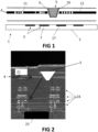
- the photonic integrated circuit device 1 comprises a planar detector 2 comprising at least one photodetector 3.
- the planar detector may comprise at least one semiconductor device layer comprising at least one photodetector configured for transducing light into an electronic signal.
- the planar detector may be planar, e.g. comprising a planar device layer or layer stack, and may be adapted for detecting light by the at least one photodetector implemented therein.
- the device may comprise an image detector that comprises an array of pixels.
- the photonic integrated circuit device further comprises a waveguide layer 4 arranged substantially parallel to the planar detector, e.g. arranged parallel to the planar detector.
- the waveguide layer may be arranged substantially parallel to the array of pixels, e.g. parallel to the array of pixels, e.g. parallel to a major plane of the image detector.
- the image detector may be for example comprise a CMOS image detector.
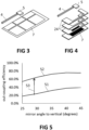
- the image detector may be a frontside-illuminated imager, e.g. may comprise metal contacts above the active pixel area, e.g. metal contact layers arranged in between the active pixel area and the waveguide layer, such as illustrated in FIG 4 , or the image detector may be backside-illuminated imager, e.g. which does not have metal contacts above the active pixel area, such as illustrated in FIG 3 .
- the image detector may be monolithically integrated in the device, e.g. the waveguide layer may be monolithically integrated on top of the image detector.
- FIG 2 shows a cross-sectional drawing of a copper sloped output mirror formed by a metal plug on a scanning electron cross-sectional micrograph of an imager pixel.
- the arrows 21 indicate the propagation direction of the light signal in operation of the device.
- the active region 23 of a pixel in this example of a front-side illuminated imager, may be positioned below a plurality of layers forming metal contacts of the imager, e.g. four layers of aluminium contacts.
- FIG 5 shows, as an illustrative example, a comparison of light out-coupling efficiency, e.g. efficiency of coupling the light signal from the waveguide to the pixel, between an exemplary embodiment comprising a frontside-illuminated imager 51 and an exemplary embodiment comprising a backside-illuminated imager 52, showing an increase of efficiency 53 of the backside-illuminated imager embodiment with respect to the frontside-illuminated imager of about a factor 2.5.
- a comparison of light out-coupling efficiency e.g. efficiency of coupling the light signal from the waveguide to the pixel
- the device may comprise a layer stack on a substrate, such as silicon on insulator wafer.
- the layer stack may comprise a buried oxide layer BOX, such as a SiO 2 BOX layer, the waveguide layer and a cladding layer, such as a SiOz layer.
- BOX buried oxide layer
- the waveguide layer and the cladding layer may successively overlie the substrate.
- the cavity may fully penetrate the waveguide layer, e.g. forming a topological hole through the waveguide layer, and may, furthermore at least partially penetrate the buried oxide layer, the cladding layer and/or the substrate.
- the waveguide layer 4 comprises a first integrated waveguide 11 for guiding at least a first light signal.
- a cavity 5, e.g. a hole, trench or indentation, is formed in the waveguide layer 4 in a region spaced away from the edges of the waveguide layer such as to terminate the first integrated waveguide 11 in this region.
- the cavity may intersect the waveguide in this region.
- the region may be spaced away from the edge of the waveguide layer by at least 5%, e.g. at least 10%, e.g. in the range of 20% to 50%, of the largest diameter of the waveguide layer.
- light traveling in the waveguide may exit the waveguide, reflect off the reflective surface and travel directly to the photodetector, e.g. without further substantial deviation from its principal line of propagation, e.g. without being substantially modified by reflective, refractive or diffractive elements between the reflective surface and an active area of the photodetector.
- the reflective surface may be formed by a material in the cavity that has a substantially different refractive index than a light-guiding core material of the waveguide.
- the reflective surface may thus form an integrated sloped output mirror for reflecting power from the waveguide toward the first photodetector of the planar detector.
- the reflective surface may be formed by a suitable reflective material, such as a metal or metal alloy, e.g. copper, aluminium, gold, silver, titanium, tantalum, or alloys of any such metal or metals.
- the reflective surface may also be formed by periodic layers of at least two different dielectric materials forming a Bragg mirror.
- the cavity may be at least partly filled with a plug to form the reflective surface.
- the cavity may be filled in with a suitable reflective fill material, such as a metal or a metal alloy, e.g. copper, aluminium, gold, silver, titanium, tantalum, or alloys of any such metal or metals.
- a suitable reflective fill material such as a metal or a metal alloy, e.g. copper, aluminium, gold, silver, titanium, tantalum, or alloys of any such metal or metals.
- a suitable reflective fill material such as a metal or a metal alloy, e.g. copper, aluminium, gold, silver, titanium, tantalum, or alloys of any such metal or metals.
- the plug may be hollow.
- the reflective material may also be coated or deposited over a facet of the integrated waveguide formed by the cavity, e.g. the reflective material, e.g. a reflective metal, may be deposited on a tilted surface of the cavity.
- the reflective surface 6 may be a reflective tilted surface forming a light coupler structure.
- the reflective tilted surface may be formed on the integrated waveguide such as to terminate the at integrated waveguide in a position that is spaced away from the edges of the waveguide layer.
- the reflective surface may be oriented at an angle in the range of 20 degrees to 60 degrees with respect to a normal direction of the waveguide layer and positioned such as to reflect light traveling in the integrated waveguide to the first photodetector 7.
- the reflective surface 6 may be provided at an angle with respect to the plane of the waveguide layer, e.g. with respect to a wafer plane on a front side of the wafer, in which this angle is in the range of 20° to 80°, e.g. in the range of 30° to 70°, for example, in the range 40° to 60°, e.g. 45°.
- FIG 5 shows an exemplary graph of light coupling efficiency, relating to the coupling of the light signal from the integrated waveguide to a pixel, as a function of the angle of the reflective surface relative to the normal of the waveguide layer, e.g. relative to a vertical direction in which the planar detector and the waveguide layer are stacked with respect to each other.
- a large light coupling efficiency can be achieved, e.g. about twice as efficient when compared to a grating coupler known in the art.
- a light coupler can be compact, e.g. more compact than a grating coupler known in the art.
- a reflective surface such as a metal reflective surface, can couple a broadband signal, e.g. a light signal comprising a large range of wavelengths can be efficiently coupled to the integrated photodetector.
- an amorphous silicon bridge may furthermore be provided between the waveguide and the reflective surface.
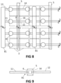
- the first integrated waveguide 11 may have a tapered section 91 in which the width of the first integrated waveguide decreases toward the first reflective surface 6, for example as illustrated in FIG 9 .
- the waveguide layer 4 also comprises a second integrated waveguide 12 for guiding a second light signal.
- This second integrated waveguide 12 is arranged such that the cavity also terminates the second integrated waveguide in the region spaced away from the edges of the waveguide layer.
- a second reflective surface 16 is provided in the cavity to reflect the second light signal when guided by the second integrated waveguide 12 toward a second photodetector 17 of the planar detector, e.g. a second pixel of the array of pixels.
- the waveguide layer may comprise a third integrated waveguide 13 and a fourth integrated waveguide 14 for guiding respectively a third light signal and a fourth light signal.
- the cavity 5 may be arranged such that it also terminates the third integrated waveguide 13 and the fourth integrated waveguide 14, in the region spaced away from the edges of the waveguide layer.
- a third reflective surface 26 and a fourth reflective surface 36 may be provided in the cavity to reflect respectively the third light signal and the fourth light signal when guided by respectively the third integrated waveguide and the fourth integrated waveguide toward respectively a third photodetector and a fourth photodetector of the planar detector.
- the first reflective surface 6, the second reflective surface 16, the third reflective surface 26 and/or the fourth reflective surface 36 may be formed by facets of a plug material in the cavity, e.g. of mirror facets of a metallic plug.
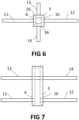
- the first, second, third and fourth integrated waveguide may be arranged in a cross shape, in which the cavity is formed in the intersection of this cross shape, for example as illustrated in FIG 6 .
- the first integrated waveguide and the second integrated waveguide may be arranged in line with each other, e.g. in each other's linear extension
- the third integrated waveguide and the fourth integrated waveguide may be arranged in line with each other, e.g. in each other's linear extension.
- the first, second, third and fourth integrated waveguide 11,12,13,14 may be arranged parallel to each other, for example, such that the first integrated waveguide 11 and the second integrated waveguide 12 are arranged in line with each other and the third integrated waveguide 13 and the fourth integrated waveguide 14 are arranged in line with each other.
- the cavity 5 may comprise an elongate trench terminating the first, second, third and fourth integrated waveguide, in which reflective surfaces are provided in the elongate trench, e.g. by a plug material filling the trench or a reflective material coated or deposited on sloped walls of the trench.
- These reflective surfaces 6,16 may thus reflect first, second, third and fourth light signals, when guided by the corresponding integrated waveguide, toward corresponding photodetectors of the planar detector, e.g. to corresponding pixels of the array of pixels.
- the first reflective surface 6 and the third reflective surface 26 may be formed by the same facet of a material in the trench, e.g. a reflective material deposited in the trench, e.g. a metallic plug in the trench, and the second reflective surface 16 and the fourth reflective surface 36 may be formed by the same facet of the material in the trench.
- embodiments of the present invention may comprise a plurality of further waveguides, arranged parallelly, such that the elongate trench intersect the plurality of further waveguides in similar manner, directing light from the further waveguides off reflective surfaces formed in the trench to corresponding photodetectors, e.g. to corresponding pixels.
- the elongate trench may be oriented at at least an angle of 45°, preferably about perpendicular, to the first, second, third and fourth integrated waveguide, and, for example, also to any further integrated waveguide.
- the integrated waveguides may be arranged in rows, while the elongate trench may be oriented in a column direction, as shown in FIG 8 .
- a photonic integrated circuit device in accordance with embodiments of the present invention may be adapted for analysing an input optical signal.
- the photonic integrated circuit device may comprise at least one light input coupler 81 for coupling the input optical signal into the first integrated waveguide, the second integrated waveguide and/or any further integrated waveguide.
- light input coupler 81 may comprise a grating coupler, embodiments of the present invention not being limited thereto.
- the at least one light input coupler may comprise a plurality of light input couplers arranged parallel to each other and substantially perpendicular to a plurality of integrated waveguides comprising the first integrated waveguide and second, third, fourth and/or further integrated waveguides as described hereinabove.
- a collimator of a radiation guiding system may collimate the input optical signal into a collimated radiation beam and a beam shaper may distribute the power of the collimated radiation beam over a discrete number of line shaped fields, in which each line shaped field is aligned with a light input coupler 81.
- the photonic integrated circuit may comprise at least one light input coupler 81 for coupling an input optical signal into the first, second, third and/or fourth integrated waveguide 11,12,13,14, wherein the, or each, light input coupler may be adapted for coupling light incident on the waveguide layer 4 into integrated waveguide segments that lie at opposite sides of the light input coupler 81, e.g. opposite sides along a direction in the plane of the waveguide layer.
- the or each light input coupler 81 may be adapted for coupling light incident on the waveguide layer into the integrated waveguide in two opposing directions simultaneously, e.g. into two segments of an integrated waveguide that lie at opposite sides of the light input coupler 81.
- the photonic integrated circuit device may comprise a plurality of elongate trenches arranged parallel to each other and substantially perpendicular to the plurality of integrated waveguides, in which the elongate trenches form cavities in the waveguide layer to terminate the integrated waveguides.
- Reflective surfaces may be provided in the elongate trenches to reflect light guided by integrated waveguides toward photodetectors 3 of the planar detector, e.g. towards pixels of the array of pixels.
- light may be coupled from either side of the trench to respectively two photodetectors on either side of and below the trench.
- the plurality of elongate trenches 5 forming light out-coupling structures for reflecting light signals from the integrated waveguides toward photodetectors and the plurality of light input couplers 81 for coupling input light into the integrated waveguides may alternate in a parallel arrangement, e.g. may form alternating columns. Since the elongate trenches may be adapted for reflecting light from integrated waveguides on either side the elongate trench to corresponding photodetectors, e.g. pixels, and the light input couplers may be adapted for coupling input light into waveguide segments on either side of the light input coupler, a compact and efficient light processing system can be achieved.
- the photonic integrated circuit device may further comprise a plurality of photonic signal processors 82, such as resonators and/or interferometer structures, arranged in and/or functionally coupled to the integrated waveguides to manipulate the spectrum of the light travelling through the integrated waveguide between a light input coupler 81 and an elongate trench.
- photonic signal processors 82 such as resonators and/or interferometer structures, arranged in and/or functionally coupled to the integrated waveguides to manipulate the spectrum of the light travelling through the integrated waveguide between a light input coupler 81 and an elongate trench.
- different photodetectors may receive differently processed light signals, even when the light input couplers receive substantially the same input light.
- the present invention also relates to a light spectrum analysis system comprising a photonic integrated circuit device in accordance with embodiments of the first aspect of the present invention.
- a spectrometer e.g. an integrated circuit spectrometer system.
- This spectrometer may comprise an photonic integrated circuit device in accordance with embodiments of the present invention.
- the spectrometer may comprise a processor for readout of the first photodetector and/or any further photodetectors, e.g. for processing signals from a plurality of photodetectors, e.g. a plurality of pixels, of the planar detector.
- the processor may be adapted for analysing such plurality of readout signals as function of corresponding spectral bands, e.g. different photodetectors may receive light signals that are processed to have different spectral content, e.g. by photonic signal processors provided in and/or functionally coupled to the integrated waveguides of the photonic integrated circuit device such as to manipulate the spectrum of the light travelling through the integrated waveguide.
- analysing the plurality of combined readout signals may comprise performing a Fourier transform spectrometric analysis method.
- the present invention also relates to a method for manufacturing a photonic integrated circuit device, such as a photonic integrated circuit device in accordance with embodiments of the first aspect of the present invention.
- the method comprises providing a layer stack, e.g. on a substrate, the layer stack comprising a buried oxide layer, a waveguide layer and a cladding layer, the waveguide layer comprising a first integrated waveguide for guiding a first light signal.
- the method also comprises forming a cavity in the waveguide layer in a region spaced away from the edges of the waveguide layer such as to terminate the first integrated waveguide in this region.
- the method further comprises providing a first reflective surface in the cavity, and arranging the layer stack on a planar detector comprising at least one photodetector, e.g. on an image detector comprising an array of pixels, such as to align the first reflective surface to reflect the first light signal when guided by the first integrated waveguide toward a first photodetector of the planar detector.
- FIG 10 illustrates an exemplary method 100 in accordance with embodiments of the present invention.
- the method 100 for manufacturing a photonic integrated circuit device comprises a step of providing 101 a layer stack, e.g. on a substrate such as a silicon-on-insulator wafer.
- the layer stack comprises a buried oxide layer 42, e.g. comprising a semiconductor oxide such as SiOz, a waveguide layer 4, e.g. comprising a waveguide core material such as a silicon nitride, and a cladding layer 41, e.g. comprising a semiconductor oxide such as SiOz.
- the buried oxide layer, the waveguide layer and the cladding layer may successively overlie each other, e.g. on the substrate.
- the waveguide layer may have a thickness of 300 nm.
- the waveguide layer comprises a first integrated waveguide 11 for guiding a first light signal.
- the method 100 also comprises forming 102 a cavity 5 in the waveguide layer in a region spaced away from the edges of the waveguide layer such as to terminate the first integrated waveguide in this region.
- forming this cavity may comprise a sloped semiconductor oxide etching process.
- Forming the cavity may comprise etching from the top surface formed by the cladding layer toward the buried oxide layer and through the waveguide layer, e.g. etching from the top surface under an angle such as to form at least one cavity wall at an angle in the range of 20 degrees to 60 degrees with respect to the normal of the waveguide layer, e.g. relative to the vertical.
- the method may further comprise providing 103 a first reflective surface in the cavity.
- providing 103 the first reflective surface may comprise depositing a seed layer on the walls of the cavity 5, e.g. as illustrated in FIG 12 .
- depositing the seed layer may comprise depositing a reflective metal seed layer, such as copper, in at the cavity, e.g. covering the walls of the cavity and the top surface of the cladding layer 41.
- Depositing the seed layer may comprise depositing tantalum nitride, tantalum and copper, e.g. a successive deposition of TaN, Ta and Cu.
- the deposited seed layer may comprise a TaN layer of about 10 nm thickness, a Ta layer of about 15 nm thickness and a Cu layer of about 100 nm thickness.
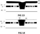
- Providing the first reflective surface in the cavity may further comprise filling the cavity with a metal 44, e.g. over the seed layer 43.
- providing the first reflective surface may comprise metal plating, e.g. by copper plating over the seed layer.
- Providing the first reflective surface may also comprise applying a planarization process, e.g. a chemical-mechanical planarization (CMP), to the top surface formed by the metal 44 over the cladding layer 41, e.g. such as to remove parts of the plating metal 44 and the seed layer 43 extending outside the cavity 5, such as illustrated in FIG 14 .
- CMP chemical-mechanical planarization
- the method 100 further comprises arranging 104 the layer stack on a planar detector, such as an image detector, e.g. a frontside-illuminated CMOS image detector or a backside-illuminated CMOS image detector.
- This planar detector comprises at least one photodetector, e.g. an array of pixels.
- the waveguide layer may be arranged substantially parallel to the planar detector.
- the first reflective surface is aligned such as to reflect the first light signal when guided by the first integrated waveguide toward a first photodetector of the planar detector, e.g. resulting in a device as shown in FIG 1 .
Landscapes
- Physics & Mathematics (AREA)
- Spectroscopy & Molecular Physics (AREA)
- General Physics & Mathematics (AREA)
- Optics & Photonics (AREA)
- Engineering & Computer Science (AREA)
- Microelectronics & Electronic Packaging (AREA)
- Power Engineering (AREA)
- Optical Integrated Circuits (AREA)
- Solid State Image Pick-Up Elements (AREA)
Claims (14)
- Un dispositif de circuit intégré photonique (1) comprenant :- un détecteur planaire (2) comprenant un premier photodétecteur (7) et un second photodétecteur (17),- une couche de guide d'ondes (4) disposée sensiblement parallèle audit détecteur planaire, la couche de guide d'ondes comprenant un premier guide d'ondes intégré (11) pour guider un premier signal lumineux, dans lequel une cavité (5) est formée dans ladite couche de guide d'ondes dans une région éloignée des bords de ladite couche de guide d'ondes de manière à terminer le premier guide d'ondes intégré dans ladite région,dans lequel une première surface réfléchissante (6) est prévue dans ladite cavité pour réfléchir le premier signal lumineux guidé par le premier guide d'ondes intégré vers le premier photodétecteur (7) dudit détecteur planaire,dans lequel ladite couche de guide d'ondes (4) comprend un second guide d'ondes intégré (12) pour guider un second signal lumineux, ledit second guide d'ondes intégré étant disposé de telle sorte que ladite cavité termine également le second guide d'ondes intégré dans ladite région éloignée des bords de la couche de guide d'ondes,et dans lequel une seconde surface réfléchissante (16) est prévue dans la cavité pour réfléchir le second signal lumineux lorsqu'il est guidé par le second guide d'ondes intégré vers le second photodétecteur (17) dudit détecteur planaire,dans lequel les premier et second guides d'ondes sont disposés en ligne l'un avec l'autre, et dans lequel la cavité (5) est agencée pour coupler la lumière hors du guide d'ondes respectif (11, 12) vers le photodétecteur respectif (7, 17).
- Le dispositif de circuit intégré photonique de la revendication 1, dans lequel ledit détecteur planaire est un détecteur d'image comprenant un réseau de pixels, dans lequel ledit au moins un photodétecteur correspond à des pixels dudit réseau de pixels.
- Le dispositif de circuit intégré photonique de la revendication 2, dans lequel ledit détecteur d'image (2) est un détecteur d'image CMOS illuminé par l'avant ou un détecteur d'image CMOS illuminé par l'arrière.
- Le dispositif de circuit intégré photonique de l'une quelconque des revendications précédentes, dans lequel ladite cavité (5) est au moins partiellement remplie avec une fiche métallique pour former ladite première surface réfléchissante (6).
- Le dispositif de circuit intégré photonique de l'une quelconque des revendications précédentes, dans lequel ladite première surface réfléchissante (6) est disposée à un angle, ledit angle entre un plan de la couche de guide d'ondes (4) et une normale à la première surface réfléchissante étant compris dans la plage de 20 degrés à 60 degrés.
- Le dispositif de circuit intégré photonique de l'une quelconque des revendications précédentes, dans lequel ledit premier guide d'ondes intégré (11) a une section effilée dans laquelle la largeur du premier guide d'ondes intégré diminue vers la première surface réfléchissante (6).
- Le dispositif de circuit intégré photonique de l'une quelconque des revendications précédentes, dans lequel ladite couche de guide d'ondes (4) comprend un troisième guide d'ondes intégré (13) et un quatrième guide d'ondes intégré (14) pour guider respectivement un troisième signal lumineux et un quatrième signal lumineux, dans lequel ladite cavité (5) termine le troisième guide d'ondes intégré et le quatrième guide d'ondes intégré, et dans lequel une troisième surface réfléchissante (26) et une quatrième surface réfléchissante (36) sont prévues dans la cavité pour réfléchir respectivement le troisième signal lumineux et le quatrième signal lumineux lorsqu'ils sont guidés respectivement par le troisième guide d'ondes intégré et le quatrième guide d'ondes intégré vers respectivement un troisième photodétecteur et un quatrième photodétecteur dudit détecteur planaire.
- Le dispositif de circuit intégré photonique de la revendication 7, dans lequel le premier guide d'ondes intégré (11), le second guide d'ondes intégré (12), le troisième guide d'ondes intégré (13) et le quatrième guide d'ondes intégré (14) sont disposés en forme de croix, ladite cavité étant formée à l'intersection de ladite forme de croix.
- Le dispositif de circuit intégré photonique de la revendication 7, dans lequel le troisième guide d'ondes intégré et le quatrième guide d'ondes intégré sont disposés en ligne l'un avec l'autre et dans lequel le premier guide d'ondes intégré (11) et le second guide d'ondes intégré (12) sont disposés parallèlement au troisième guide d'ondes intégré (13) et au quatrième guide d'ondes intégré (14), ladite cavité (5) comprenant une tranchée allongée terminant les premier, second, troisième et quatrième guides d'ondes intégrés.
- Le dispositif de circuit intégré photonique de la revendication 9, dans lequel la tranchée allongée est orientée perpendiculairement aux premier, second, troisième et quatrième guides d'ondes intégrés (11,12,13,14), et dans lequel le premier guide d'ondes intégré (11) et le second guide d'ondes intégré (13) se trouvent à des côtés opposés de la tranchée allongée, et dans lequel le troisième guide d'ondes intégré (13) et le quatrième guide d'ondes intégré (14) se trouvent à des côtés opposés de la tranchée allongée.
- Le dispositif de circuit intégré photonique de la revendication 10, comprenant en outre au moins un coupleur d'entrée de lumière (81) pour coupler un signal optique d'entrée dans le premier, second, troisième et/ou quatrième guide d'ondes intégré (11,12,13,14), dans lequel chacun dudit au moins un coupleur d'entrée de lumière est adapté pour coupler la lumière incidente sur la couche de guide d'ondes (4) dans des segments de guide d'ondes intégrés qui se trouvent à des côtés opposés du coupleur d'entrée de lumière (81).
- Le dispositif de circuit intégré photonique de la revendication 11, dans lequel une pluralité de tranchées allongées et une pluralité de coupleurs d'entrée de lumière (81) alternent dans un agencement parallèle, le dispositif de circuit intégré photonique comprenant en outre une pluralité de processeurs de signal photonique (82) disposés dans et/ou fonctionnellement couplés aux guides d'ondes intégrés pour manipuler le spectre de la lumière voyageant à travers le guide d'ondes intégré entre un coupleur d'entrée de lumière (81) et une tranchée allongée.
- Un spectromètre comprenant un dispositif de circuit intégré photonique selon l'une quelconque des revendications précédentes.
- Un procédé (100) de fabrication d'un dispositif de circuit intégré photonique, le procédé comprenant :- la fourniture (101) d'un empilement de couches comprenant une couche d'oxyde enterrée, une couche de guide d'ondes (4) et une couche de revêtement, la couche de guide d'ondes comprenant un premier guide d'ondes intégré (11) pour guider un premier signal lumineux, et un second guide d'ondes intégré (12) en ligne avec le premier guide d'ondes (11) pour guider un second signal lumineux,- la formation (102) d'une cavité (5) dans ladite couche de guide d'ondes (4) dans une région éloignée des bords de ladite couche de guide d'ondes de manière à terminer le premier guide d'ondes intégré dans ladite région et à terminer le second guide d'ondes intégré dans ladite région, pour coupler la lumière hors du guide d'ondes respectif,- la fourniture (103) d'une première surface réfléchissante (6) dans ladite cavité, et d'une seconde surface réfléchissante (16) dans ladite cavité, et- l'agencement (104) dudit empilement de couches sur un détecteur planaire (2) comprenant un premier photodétecteur (7) et un second photodétecteur (17) de manière à aligner ladite première surface réfléchissante pour réfléchir le premier signal lumineux lorsqu'il est guidé par le premier guide d'ondes intégré vers le premier photodétecteur (7) dudit détecteur planaire et ladite seconde surface réfléchissante pour réfléchir le second signal lumineux lorsqu'il est guidé par le second guide d'ondes intégré vers le second photodétecteur (17) dudit détecteur planaire.
Priority Applications (3)
| Application Number | Priority Date | Filing Date | Title |
|---|---|---|---|
| EP16202279.2A EP3330759B1 (fr) | 2016-12-05 | 2016-12-05 | Coupleur de lumière à circuit photonique et procédé associé |
| KR1020170166022A KR102543819B1 (ko) | 2016-12-05 | 2017-12-05 | 분광계, 광자 집적 회로 장치 및 그 제조방법 |
| US15/831,565 US10451821B2 (en) | 2016-12-05 | 2017-12-05 | Photonic circuit light coupler |
Applications Claiming Priority (1)
| Application Number | Priority Date | Filing Date | Title |
|---|---|---|---|
| EP16202279.2A EP3330759B1 (fr) | 2016-12-05 | 2016-12-05 | Coupleur de lumière à circuit photonique et procédé associé |
Publications (2)
| Publication Number | Publication Date |
|---|---|
| EP3330759A1 EP3330759A1 (fr) | 2018-06-06 |
| EP3330759B1 true EP3330759B1 (fr) | 2025-02-12 |
Family
ID=57482340
Family Applications (1)
| Application Number | Title | Priority Date | Filing Date |
|---|---|---|---|
| EP16202279.2A Active EP3330759B1 (fr) | 2016-12-05 | 2016-12-05 | Coupleur de lumière à circuit photonique et procédé associé |
Country Status (3)
| Country | Link |
|---|---|
| US (1) | US10451821B2 (fr) |
| EP (1) | EP3330759B1 (fr) |
| KR (1) | KR102543819B1 (fr) |
Families Citing this family (3)
| Publication number | Priority date | Publication date | Assignee | Title |
|---|---|---|---|---|
| EP3842845A1 (fr) * | 2019-12-23 | 2021-06-30 | Ams Ag | Dispositif à semiconducteurs et procédé de fabrication de dispositif à semiconducteurs |
| US10955614B1 (en) * | 2020-01-14 | 2021-03-23 | Globalfoundries U.S. Inc. | Optical fiber coupler structure having manufacturing variation-sensitive transmission blocking region |
| EP4033282A1 (fr) * | 2021-01-26 | 2022-07-27 | AIT Austrian Institute of Technology GmbH | Circuit intégré photonique |
Citations (4)
| Publication number | Priority date | Publication date | Assignee | Title |
|---|---|---|---|---|
| EP0481464A2 (fr) * | 1990-10-17 | 1992-04-22 | Canon Kabushiki Kaisha | Dispositif optique avec un coupleur optique pour effectuer une séparation/combinaison de lumière par division du front d'onde |
| US5170448A (en) * | 1992-01-06 | 1992-12-08 | Motorola, Inc. | Optical waveguide apparatus and method for partially collecting light |
| WO2010023976A1 (fr) * | 2008-08-26 | 2010-03-04 | 住友ベークライト株式会社 | Guide d’ondes optique, module à guide d’ondes optique et substrat de montage d’un élément optique |
| US20140001493A1 (en) * | 2012-07-02 | 2014-01-02 | Stmicroelectronics S.R.L | Integrated optoelectronic device and system with waveguide and manufacturing process thereof |
Family Cites Families (22)
| Publication number | Priority date | Publication date | Assignee | Title |
|---|---|---|---|---|
| US4990465A (en) * | 1985-01-22 | 1991-02-05 | Massachusetts Institute Of Technology | Method of forming a surface emitting laser |
| US5357122A (en) * | 1991-09-05 | 1994-10-18 | Sony Corporation | Three-dimensional optical-electronic integrated circuit device with raised sections |
| US7599277B1 (en) * | 1998-11-09 | 2009-10-06 | Seiko Instruments Inc. | Near-field optical head having tapered hole for guiding light beam |
| US6226083B1 (en) | 1999-05-05 | 2001-05-01 | Georgia Tech Research Corporation | Integrated-optic spectrometer and method |
| JP3764640B2 (ja) * | 2000-09-26 | 2006-04-12 | 京セラ株式会社 | 光モジュール及びその製造方法 |
| JP3762208B2 (ja) * | 2000-09-29 | 2006-04-05 | 株式会社東芝 | 光配線基板の製造方法 |
| US6563997B1 (en) * | 2000-11-28 | 2003-05-13 | Lighteross, Inc. | Formation of a surface on an optical component |
| EP1286194A3 (fr) * | 2001-08-21 | 2004-05-19 | Canon Kabushiki Kaisha | Dispositif guide d'ondes optiques |
| US6801679B2 (en) * | 2001-11-23 | 2004-10-05 | Seungug Koh | Multifunctional intelligent optical modules based on planar lightwave circuits |
| US7095537B2 (en) * | 2003-05-30 | 2006-08-22 | General Electric Company | Method and system for optical coupling using holographic recording media |
| US7112885B2 (en) * | 2003-07-07 | 2006-09-26 | Board Of Regents, The University Of Texas System | System, method and apparatus for improved electrical-to-optical transmitters disposed within printed circuit boards |
| US7916986B2 (en) * | 2004-03-15 | 2011-03-29 | Sharp Laboratories Of America, Inc. | Erbium-doped silicon nanocrystalline embedded silicon oxide waveguide |
| CN101147088B (zh) * | 2005-02-16 | 2011-08-17 | 应用材料股份有限公司 | 光学耦合至ic芯片 |
| KR100802199B1 (ko) * | 2006-05-25 | 2008-03-17 | 정경희 | 광모듈 및 그 제조방법 |
| JP4825729B2 (ja) * | 2007-05-24 | 2011-11-30 | 日東電工株式会社 | 光導波路デバイスおよびその製造方法 |
| KR101251028B1 (ko) * | 2008-04-26 | 2013-04-04 | 광주과학기술원 | 광배선 구조물 및 그 제조방법 |
| EP2488912B1 (fr) * | 2009-10-12 | 2019-07-24 | The Trustees Of Columbia University In The City Of New York | Guide d'onde comprenant un cristal photonique pour l'extraction de lumère à des longueurs d'onde spécifiques |
| TWI498617B (zh) * | 2010-10-01 | 2015-09-01 | Sumitomo Bakelite Co | 光導波路構造體及電子機器 |
| US9042696B2 (en) * | 2010-12-20 | 2015-05-26 | Intel Corporation | Method and structure combining vertical and angled facets in silicon photonic waveguides |
| JP2012151157A (ja) * | 2011-01-17 | 2012-08-09 | Hitachi Ltd | 水平共振器垂直出射レーザとその製造方法及び受光素子、並びに水平共振器垂直出射レーザアレイ |
| US9086551B2 (en) * | 2013-10-30 | 2015-07-21 | International Business Machines Corporation | Double mirror structure for wavelength division multiplexing with polymer waveguides |
| EP2913663A1 (fr) | 2014-02-28 | 2015-09-02 | IMEC vzw | Spectromètre optique à portée adaptée |
-
2016
- 2016-12-05 EP EP16202279.2A patent/EP3330759B1/fr active Active
-
2017
- 2017-12-05 US US15/831,565 patent/US10451821B2/en active Active
- 2017-12-05 KR KR1020170166022A patent/KR102543819B1/ko active Active
Patent Citations (4)
| Publication number | Priority date | Publication date | Assignee | Title |
|---|---|---|---|---|
| EP0481464A2 (fr) * | 1990-10-17 | 1992-04-22 | Canon Kabushiki Kaisha | Dispositif optique avec un coupleur optique pour effectuer une séparation/combinaison de lumière par division du front d'onde |
| US5170448A (en) * | 1992-01-06 | 1992-12-08 | Motorola, Inc. | Optical waveguide apparatus and method for partially collecting light |
| WO2010023976A1 (fr) * | 2008-08-26 | 2010-03-04 | 住友ベークライト株式会社 | Guide d’ondes optique, module à guide d’ondes optique et substrat de montage d’un élément optique |
| US20140001493A1 (en) * | 2012-07-02 | 2014-01-02 | Stmicroelectronics S.R.L | Integrated optoelectronic device and system with waveguide and manufacturing process thereof |
Also Published As
| Publication number | Publication date |
|---|---|
| US20180156991A1 (en) | 2018-06-07 |
| US10451821B2 (en) | 2019-10-22 |
| KR102543819B1 (ko) | 2023-06-14 |
| EP3330759A1 (fr) | 2018-06-06 |
| KR20180064318A (ko) | 2018-06-14 |
Similar Documents
| Publication | Publication Date | Title |
|---|---|---|
| US7376308B2 (en) | Optical off-chip interconnects in multichannel planar waveguide devices | |
| CN112673274B (zh) | Lidar输出信号的导引中的相位控制 | |
| EP3839454B1 (fr) | Filtre spectral de polarisation, matrice de filtres, et capteur spectral de polarisation | |
| US9482816B2 (en) | Radiation coupler | |
| EP3028307B1 (fr) | Capteur d'image à semi-conducteurs, et appareil de capture d'image utilisant ce capteur | |
| EP2677356B1 (fr) | Module optoélectronique intégré | |
| KR20160019779A (ko) | 광 다이오드를 가지는 광전 변환 소자 및 광 신호 수신 유닛 | |
| US11326946B2 (en) | Integrated bound-mode spectral sensors with chirped gratings | |
| US10451821B2 (en) | Photonic circuit light coupler | |
| US7409123B1 (en) | Grating having reduced mode dispersion | |
| CN102637710A (zh) | 光电转换元件、光电转换装置和图像感测系统 | |
| US11049892B2 (en) | Image sensor | |
| US11187852B1 (en) | Bragg gratings with silicide-coated segments | |
| US7945131B1 (en) | System having optical amplifier incorporated into stacked optical devices | |
| US20210263219A1 (en) | Planar Lightwave Circuit and Optical Device | |
| EP2026051B1 (fr) | Dispositif de spectroscopie, appareil de spectroscopie et procédé de spectroscopie | |
| KR102891313B1 (ko) | 메타물질 층을 포함하는 에지 커플러들 | |
| US11175453B2 (en) | Photonic circuit with integrated light coupler | |
| JP5821400B2 (ja) | 分光センサー及び角度制限フィルター | |
| TWI923047B (zh) | 用於光耦合的裝置、用於製造光學裝置的方法 | |
| CN114122168A (zh) | 用于光学感测的器件及其制造方法 | |
| TWI892285B (zh) | 光信號測量設備及其製造方法、以及光信號測量方法 | |
| US12529843B2 (en) | Photonics chip structures including a reflector | |
| US12560762B2 (en) | Reflectors for a photonics chip | |
| TW202538342A (zh) | 用於光耦合的裝置、用於製造光學裝置的方法 |
Legal Events
| Date | Code | Title | Description |
|---|---|---|---|
| PUAI | Public reference made under article 153(3) epc to a published international application that has entered the european phase |
Free format text: ORIGINAL CODE: 0009012 |
|
| STAA | Information on the status of an ep patent application or granted ep patent |
Free format text: STATUS: THE APPLICATION HAS BEEN PUBLISHED |
|
| AK | Designated contracting states |
Kind code of ref document: A1 Designated state(s): AL AT BE BG CH CY CZ DE DK EE ES FI FR GB GR HR HU IE IS IT LI LT LU LV MC MK MT NL NO PL PT RO RS SE SI SK SM TR |
|
| AX | Request for extension of the european patent |
Extension state: BA ME |
|
| STAA | Information on the status of an ep patent application or granted ep patent |
Free format text: STATUS: REQUEST FOR EXAMINATION WAS MADE |
|
| 17P | Request for examination filed |
Effective date: 20181202 |
|
| RBV | Designated contracting states (corrected) |
Designated state(s): AL AT BE BG CH CY CZ DE DK EE ES FI FR GB GR HR HU IE IS IT LI LT LU LV MC MK MT NL NO PL PT RO RS SE SI SK SM TR |
|
| STAA | Information on the status of an ep patent application or granted ep patent |
Free format text: STATUS: EXAMINATION IS IN PROGRESS |
|
| 17Q | First examination report despatched |
Effective date: 20200623 |
|
| GRAP | Despatch of communication of intention to grant a patent |
Free format text: ORIGINAL CODE: EPIDOSNIGR1 |
|
| STAA | Information on the status of an ep patent application or granted ep patent |
Free format text: STATUS: GRANT OF PATENT IS INTENDED |
|
| INTG | Intention to grant announced |
Effective date: 20240917 |
|
| P01 | Opt-out of the competence of the unified patent court (upc) registered |
Free format text: CASE NUMBER: APP_53767/2024 Effective date: 20240927 |
|
| GRAS | Grant fee paid |
Free format text: ORIGINAL CODE: EPIDOSNIGR3 |
|
| GRAA | (expected) grant |
Free format text: ORIGINAL CODE: 0009210 |
|
| STAA | Information on the status of an ep patent application or granted ep patent |
Free format text: STATUS: THE PATENT HAS BEEN GRANTED |
|
| AK | Designated contracting states |
Kind code of ref document: B1 Designated state(s): AL AT BE BG CH CY CZ DE DK EE ES FI FR GB GR HR HU IE IS IT LI LT LU LV MC MK MT NL NO PL PT RO RS SE SI SK SM TR |
|
| REG | Reference to a national code |
Ref country code: GB Ref legal event code: FG4D |
|
| REG | Reference to a national code |
Ref country code: CH Ref legal event code: EP |
|
| REG | Reference to a national code |
Ref country code: DE Ref legal event code: R096 Ref document number: 602016091174 Country of ref document: DE |
|
| REG | Reference to a national code |
Ref country code: IE Ref legal event code: FG4D |
|
| REG | Reference to a national code |
Ref country code: NL Ref legal event code: MP Effective date: 20250212 |
|
| PG25 | Lapsed in a contracting state [announced via postgrant information from national office to epo] |
Ref country code: RS Free format text: LAPSE BECAUSE OF FAILURE TO SUBMIT A TRANSLATION OF THE DESCRIPTION OR TO PAY THE FEE WITHIN THE PRESCRIBED TIME-LIMIT Effective date: 20250512 |
|
| PG25 | Lapsed in a contracting state [announced via postgrant information from national office to epo] |
Ref country code: FI Free format text: LAPSE BECAUSE OF FAILURE TO SUBMIT A TRANSLATION OF THE DESCRIPTION OR TO PAY THE FEE WITHIN THE PRESCRIBED TIME-LIMIT Effective date: 20250212 |
|
| PG25 | Lapsed in a contracting state [announced via postgrant information from national office to epo] |
Ref country code: PL Free format text: LAPSE BECAUSE OF FAILURE TO SUBMIT A TRANSLATION OF THE DESCRIPTION OR TO PAY THE FEE WITHIN THE PRESCRIBED TIME-LIMIT Effective date: 20250212 |
|
| PG25 | Lapsed in a contracting state [announced via postgrant information from national office to epo] |
Ref country code: ES Free format text: LAPSE BECAUSE OF FAILURE TO SUBMIT A TRANSLATION OF THE DESCRIPTION OR TO PAY THE FEE WITHIN THE PRESCRIBED TIME-LIMIT Effective date: 20250212 |
|
| REG | Reference to a national code |
Ref country code: LT Ref legal event code: MG9D |
|
| PG25 | Lapsed in a contracting state [announced via postgrant information from national office to epo] |
Ref country code: IS Free format text: LAPSE BECAUSE OF FAILURE TO SUBMIT A TRANSLATION OF THE DESCRIPTION OR TO PAY THE FEE WITHIN THE PRESCRIBED TIME-LIMIT Effective date: 20250612 Ref country code: NO Free format text: LAPSE BECAUSE OF FAILURE TO SUBMIT A TRANSLATION OF THE DESCRIPTION OR TO PAY THE FEE WITHIN THE PRESCRIBED TIME-LIMIT Effective date: 20250512 |
|
| PG25 | Lapsed in a contracting state [announced via postgrant information from national office to epo] |
Ref country code: NL Free format text: LAPSE BECAUSE OF FAILURE TO SUBMIT A TRANSLATION OF THE DESCRIPTION OR TO PAY THE FEE WITHIN THE PRESCRIBED TIME-LIMIT Effective date: 20250212 |
|
| PG25 | Lapsed in a contracting state [announced via postgrant information from national office to epo] |
Ref country code: HR Free format text: LAPSE BECAUSE OF FAILURE TO SUBMIT A TRANSLATION OF THE DESCRIPTION OR TO PAY THE FEE WITHIN THE PRESCRIBED TIME-LIMIT Effective date: 20250212 |
|
| PG25 | Lapsed in a contracting state [announced via postgrant information from national office to epo] |
Ref country code: PT Free format text: LAPSE BECAUSE OF FAILURE TO SUBMIT A TRANSLATION OF THE DESCRIPTION OR TO PAY THE FEE WITHIN THE PRESCRIBED TIME-LIMIT Effective date: 20250612 Ref country code: LV Free format text: LAPSE BECAUSE OF FAILURE TO SUBMIT A TRANSLATION OF THE DESCRIPTION OR TO PAY THE FEE WITHIN THE PRESCRIBED TIME-LIMIT Effective date: 20250212 |
|
| PG25 | Lapsed in a contracting state [announced via postgrant information from national office to epo] |
Ref country code: BG Free format text: LAPSE BECAUSE OF FAILURE TO SUBMIT A TRANSLATION OF THE DESCRIPTION OR TO PAY THE FEE WITHIN THE PRESCRIBED TIME-LIMIT Effective date: 20250212 Ref country code: GR Free format text: LAPSE BECAUSE OF FAILURE TO SUBMIT A TRANSLATION OF THE DESCRIPTION OR TO PAY THE FEE WITHIN THE PRESCRIBED TIME-LIMIT Effective date: 20250513 |
|
| REG | Reference to a national code |
Ref country code: AT Ref legal event code: MK05 Ref document number: 1766568 Country of ref document: AT Kind code of ref document: T Effective date: 20250212 |
|
| PG25 | Lapsed in a contracting state [announced via postgrant information from national office to epo] |
Ref country code: SE Free format text: LAPSE BECAUSE OF FAILURE TO SUBMIT A TRANSLATION OF THE DESCRIPTION OR TO PAY THE FEE WITHIN THE PRESCRIBED TIME-LIMIT Effective date: 20250212 |
|
| PG25 | Lapsed in a contracting state [announced via postgrant information from national office to epo] |
Ref country code: SM Free format text: LAPSE BECAUSE OF FAILURE TO SUBMIT A TRANSLATION OF THE DESCRIPTION OR TO PAY THE FEE WITHIN THE PRESCRIBED TIME-LIMIT Effective date: 20250212 |
|
| PG25 | Lapsed in a contracting state [announced via postgrant information from national office to epo] |
Ref country code: DK Free format text: LAPSE BECAUSE OF FAILURE TO SUBMIT A TRANSLATION OF THE DESCRIPTION OR TO PAY THE FEE WITHIN THE PRESCRIBED TIME-LIMIT Effective date: 20250212 |
|
| PG25 | Lapsed in a contracting state [announced via postgrant information from national office to epo] |
Ref country code: IT Free format text: LAPSE BECAUSE OF FAILURE TO SUBMIT A TRANSLATION OF THE DESCRIPTION OR TO PAY THE FEE WITHIN THE PRESCRIBED TIME-LIMIT Effective date: 20250212 |
|
| PG25 | Lapsed in a contracting state [announced via postgrant information from national office to epo] |
Ref country code: AT Free format text: LAPSE BECAUSE OF FAILURE TO SUBMIT A TRANSLATION OF THE DESCRIPTION OR TO PAY THE FEE WITHIN THE PRESCRIBED TIME-LIMIT Effective date: 20250212 |
|
| PG25 | Lapsed in a contracting state [announced via postgrant information from national office to epo] |
Ref country code: EE Free format text: LAPSE BECAUSE OF FAILURE TO SUBMIT A TRANSLATION OF THE DESCRIPTION OR TO PAY THE FEE WITHIN THE PRESCRIBED TIME-LIMIT Effective date: 20250212 Ref country code: CZ Free format text: LAPSE BECAUSE OF FAILURE TO SUBMIT A TRANSLATION OF THE DESCRIPTION OR TO PAY THE FEE WITHIN THE PRESCRIBED TIME-LIMIT Effective date: 20250212 |
|
| PG25 | Lapsed in a contracting state [announced via postgrant information from national office to epo] |
Ref country code: RO Free format text: LAPSE BECAUSE OF FAILURE TO SUBMIT A TRANSLATION OF THE DESCRIPTION OR TO PAY THE FEE WITHIN THE PRESCRIBED TIME-LIMIT Effective date: 20250212 |
|
| PG25 | Lapsed in a contracting state [announced via postgrant information from national office to epo] |
Ref country code: SK Free format text: LAPSE BECAUSE OF FAILURE TO SUBMIT A TRANSLATION OF THE DESCRIPTION OR TO PAY THE FEE WITHIN THE PRESCRIBED TIME-LIMIT Effective date: 20250212 |
|
| REG | Reference to a national code |
Ref country code: DE Ref legal event code: R097 Ref document number: 602016091174 Country of ref document: DE |
|
| PLBE | No opposition filed within time limit |
Free format text: ORIGINAL CODE: 0009261 |
|
| STAA | Information on the status of an ep patent application or granted ep patent |
Free format text: STATUS: NO OPPOSITION FILED WITHIN TIME LIMIT |
|
| PGFP | Annual fee paid to national office [announced via postgrant information from national office to epo] |
Ref country code: DE Payment date: 20251126 Year of fee payment: 10 |
|
| 26N | No opposition filed |
Effective date: 20251113 |