EP3349139B1 - Körper eines kartenlesegeräts mit gesichertem speicher - Google Patents
Körper eines kartenlesegeräts mit gesichertem speicher Download PDFInfo
- Publication number
- EP3349139B1 EP3349139B1 EP18150857.3A EP18150857A EP3349139B1 EP 3349139 B1 EP3349139 B1 EP 3349139B1 EP 18150857 A EP18150857 A EP 18150857A EP 3349139 B1 EP3349139 B1 EP 3349139B1
- Authority
- EP
- European Patent Office
- Prior art keywords
- memory card
- upper cover
- card reader
- printed circuit
- reader body
- Prior art date
- Legal status (The legal status is an assumption and is not a legal conclusion. Google has not performed a legal analysis and makes no representation as to the accuracy of the status listed.)
- Active
Links
Images

Classifications
-
- H—ELECTRICITY
- H01—ELECTRIC ELEMENTS
- H01R—ELECTRICALLY-CONDUCTIVE CONNECTIONS; STRUCTURAL ASSOCIATIONS OF A PLURALITY OF MUTUALLY-INSULATED ELECTRICAL CONNECTING ELEMENTS; COUPLING DEVICES; CURRENT COLLECTORS
- H01R13/00—Details of coupling devices of the kinds covered by groups H01R12/70 or H01R24/00 - H01R33/00
- H01R13/44—Means for preventing access to live contacts
- H01R13/447—Shutter or cover plate
-
- G—PHYSICS
- G06—COMPUTING OR CALCULATING; COUNTING
- G06F—ELECTRIC DIGITAL DATA PROCESSING
- G06F21/00—Security arrangements for protecting computers, components thereof, programs or data against unauthorised activity
- G06F21/70—Protecting specific internal or peripheral components, in which the protection of a component leads to protection of the entire computer
- G06F21/86—Secure or tamper-resistant housings
-
- G—PHYSICS
- G06—COMPUTING OR CALCULATING; COUNTING
- G06K—GRAPHICAL DATA READING; PRESENTATION OF DATA; RECORD CARRIERS; HANDLING RECORD CARRIERS
- G06K7/00—Methods or arrangements for sensing record carriers, e.g. for reading patterns
- G06K7/0004—Hybrid readers
-
- G—PHYSICS
- G06—COMPUTING OR CALCULATING; COUNTING
- G06K—GRAPHICAL DATA READING; PRESENTATION OF DATA; RECORD CARRIERS; HANDLING RECORD CARRIERS
- G06K7/00—Methods or arrangements for sensing record carriers, e.g. for reading patterns
- G06K7/0013—Methods or arrangements for sensing record carriers, e.g. for reading patterns by galvanic contacts, e.g. card connectors for ISO-7816 compliant smart cards or memory cards, e.g. SD card readers
- G06K7/0021—Methods or arrangements for sensing record carriers, e.g. for reading patterns by galvanic contacts, e.g. card connectors for ISO-7816 compliant smart cards or memory cards, e.g. SD card readers for reading/sensing record carriers having surface contacts
-
- G—PHYSICS
- G06—COMPUTING OR CALCULATING; COUNTING
- G06K—GRAPHICAL DATA READING; PRESENTATION OF DATA; RECORD CARRIERS; HANDLING RECORD CARRIERS
- G06K7/00—Methods or arrangements for sensing record carriers, e.g. for reading patterns
- G06K7/0013—Methods or arrangements for sensing record carriers, e.g. for reading patterns by galvanic contacts, e.g. card connectors for ISO-7816 compliant smart cards or memory cards, e.g. SD card readers
- G06K7/0056—Methods or arrangements for sensing record carriers, e.g. for reading patterns by galvanic contacts, e.g. card connectors for ISO-7816 compliant smart cards or memory cards, e.g. SD card readers housing of the card connector
-
- G—PHYSICS
- G06—COMPUTING OR CALCULATING; COUNTING
- G06K—GRAPHICAL DATA READING; PRESENTATION OF DATA; RECORD CARRIERS; HANDLING RECORD CARRIERS
- G06K7/00—Methods or arrangements for sensing record carriers, e.g. for reading patterns
- G06K7/0013—Methods or arrangements for sensing record carriers, e.g. for reading patterns by galvanic contacts, e.g. card connectors for ISO-7816 compliant smart cards or memory cards, e.g. SD card readers
- G06K7/0056—Methods or arrangements for sensing record carriers, e.g. for reading patterns by galvanic contacts, e.g. card connectors for ISO-7816 compliant smart cards or memory cards, e.g. SD card readers housing of the card connector
- G06K7/0078—Methods or arrangements for sensing record carriers, e.g. for reading patterns by galvanic contacts, e.g. card connectors for ISO-7816 compliant smart cards or memory cards, e.g. SD card readers housing of the card connector reinforced housing for protection against damage, be it due malevolent action, such as drilling and other ways of forced entry, or by accident, such as shock due to dropping
-
- G—PHYSICS
- G06—COMPUTING OR CALCULATING; COUNTING
- G06K—GRAPHICAL DATA READING; PRESENTATION OF DATA; RECORD CARRIERS; HANDLING RECORD CARRIERS
- G06K7/00—Methods or arrangements for sensing record carriers, e.g. for reading patterns
- G06K7/0013—Methods or arrangements for sensing record carriers, e.g. for reading patterns by galvanic contacts, e.g. card connectors for ISO-7816 compliant smart cards or memory cards, e.g. SD card readers
- G06K7/0056—Methods or arrangements for sensing record carriers, e.g. for reading patterns by galvanic contacts, e.g. card connectors for ISO-7816 compliant smart cards or memory cards, e.g. SD card readers housing of the card connector
- G06K7/0082—Methods or arrangements for sensing record carriers, e.g. for reading patterns by galvanic contacts, e.g. card connectors for ISO-7816 compliant smart cards or memory cards, e.g. SD card readers housing of the card connector comprising an arrangement for protection against electrostatic discharge, e.g. by grounding part of the conductive housing
-
- G—PHYSICS
- G06—COMPUTING OR CALCULATING; COUNTING
- G06K—GRAPHICAL DATA READING; PRESENTATION OF DATA; RECORD CARRIERS; HANDLING RECORD CARRIERS
- G06K7/00—Methods or arrangements for sensing record carriers, e.g. for reading patterns
- G06K7/0013—Methods or arrangements for sensing record carriers, e.g. for reading patterns by galvanic contacts, e.g. card connectors for ISO-7816 compliant smart cards or memory cards, e.g. SD card readers
- G06K7/0086—Methods or arrangements for sensing record carriers, e.g. for reading patterns by galvanic contacts, e.g. card connectors for ISO-7816 compliant smart cards or memory cards, e.g. SD card readers the connector comprising a circuit for steering the operations of the card connector
- G06K7/0091—Methods or arrangements for sensing record carriers, e.g. for reading patterns by galvanic contacts, e.g. card connectors for ISO-7816 compliant smart cards or memory cards, e.g. SD card readers the connector comprising a circuit for steering the operations of the card connector the circuit comprising an arrangement for avoiding intrusions and unwanted access to data inside of the connector
-
- H—ELECTRICITY
- H01—ELECTRIC ELEMENTS
- H01R—ELECTRICALLY-CONDUCTIVE CONNECTIONS; STRUCTURAL ASSOCIATIONS OF A PLURALITY OF MUTUALLY-INSULATED ELECTRICAL CONNECTING ELEMENTS; COUPLING DEVICES; CURRENT COLLECTORS
- H01R12/00—Structural associations of a plurality of mutually-insulated electrical connecting elements, specially adapted for printed circuits, e.g. printed circuit boards [PCB], flat or ribbon cables, or like generally planar structures, e.g. terminal strips, terminal blocks; Coupling devices specially adapted for printed circuits, flat or ribbon cables, or like generally planar structures; Terminals specially adapted for contact with, or insertion into, printed circuits, flat or ribbon cables, or like generally planar structures
- H01R12/70—Coupling devices
- H01R12/7005—Guiding, mounting, polarizing or locking means; Extractors
-
- H—ELECTRICITY
- H01—ELECTRIC ELEMENTS
- H01R—ELECTRICALLY-CONDUCTIVE CONNECTIONS; STRUCTURAL ASSOCIATIONS OF A PLURALITY OF MUTUALLY-INSULATED ELECTRICAL CONNECTING ELEMENTS; COUPLING DEVICES; CURRENT COLLECTORS
- H01R12/00—Structural associations of a plurality of mutually-insulated electrical connecting elements, specially adapted for printed circuits, e.g. printed circuit boards [PCB], flat or ribbon cables, or like generally planar structures, e.g. terminal strips, terminal blocks; Coupling devices specially adapted for printed circuits, flat or ribbon cables, or like generally planar structures; Terminals specially adapted for contact with, or insertion into, printed circuits, flat or ribbon cables, or like generally planar structures
- H01R12/70—Coupling devices
- H01R12/71—Coupling devices for rigid printing circuits or like structures
- H01R12/712—Coupling devices for rigid printing circuits or like structures co-operating with the surface of the printed circuit or with a coupling device exclusively provided on the surface of the printed circuit
-
- H—ELECTRICITY
- H05—ELECTRIC TECHNIQUES NOT OTHERWISE PROVIDED FOR
- H05F—STATIC ELECTRICITY; NATURALLY-OCCURRING ELECTRICITY
- H05F3/00—Carrying-off electrostatic charges
- H05F3/02—Carrying-off electrostatic charges by means of earthing connections
Definitions
- the invention lies in the field of memory card readers.
- the invention more particularly relates to a memory card reader intended to be mounted in a memory card reading terminal.
- a terminal can be a payment terminal, an identification terminal.
- the invention relates to any type of terminal that can include a memory card reader.
- Memory card reading terminals include, in addition to a memory card reader, a certain number of components such as a keyboard, a screen, one or more processors, memory, and an electrical power source. For several years, memory card reading terminals have seen their functions multiply. This is particularly true for payment terminals. In addition to the payment function, the terminals include network communication functions, detection functions for contactless memory cards (“contactless” cards), coupon management functions (for example loyalty coupons), etc.
- the memory card reader in fact, remains a weak link in the memory card reading terminal. This is due to the fact that the memory card reader includes a memory card insertion slot, this slot making the interior of the terminal accessible from the outside. More particularly, Attackers seek to gain access to the memory card slot.
- the memory card connector is the part of the memory card reader that comes into contact with the chip or microprocessor embedded in the memory card.
- memory card readers have been provided with mesh protection. This protection makes it possible to avoid introduction by drilling the terminal. When an object attempts to penetrate the protective enclosure, a short circuit is produced, causing the terminal to be taken out of service.
- modifications to protect memory card connectors against electrostatic discharge and wear have also been proposed. This involves, for example, placing, at the entrance to the memory card reader, metal parts ensuring mechanical guidance (prevention against wear) and/or discharge of the card prior to its insertion into the memory card reader.
- these metal parts are in the form of metal guide rods a few millimeters high.
- Another example is to add metal parts that are in the form of a discharge comb from the board.
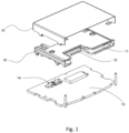
- This memory card reader comprises a memory card reader body 10, comprising a memory card insertion slot 11.
- the memory card connector is directly integrated into the memory card reader. It includes pins 12 for connection to a printed circuit 13 (partial view) making it possible to ensure the operation of the reader and its interconnection with the other components of the device within which it is installed (this printed circuit 13 is generally the motherboard of the memory card reading terminal).
- this printed circuit 13 also includes electronic components 14. To protect the memory card reader 10, it is covered with a complete protection 15, as well as a front protection (not shown).
- the document FR 2 889 756 discloses a molded plastic card body, to which is glued or fixed a mesh (several densities are shown) which can extend over the entire face of the card body.
- the interior or exterior faces are considered in different embodiment examples.
- the invention is defined by the independent claims. Several embodiment examples are given in the dependent claims.
- This technique makes it possible to partly resolve the problems posed by the prior art.
- the present technique relates in fact to a memory card reader body comprising a slot for inserting a memory card and a housing for receiving a memory card connector, said reader body comprising an upper cover and a lower base.
- Such a memory card reader body differs from known reader bodies in that it comprises a third part, distinct from the lower base or the upper cover. This third part takes the form of a printed circuit fixed on an upper face of said upper cover, said printed circuit comprising at least one protective element.
- the proposed three-part architecture allows the implementation of a memory card reader body that is less expensive and easier to produce compared to the solutions of the prior art, but which nevertheless offers a level high protection against fraudulent attempts to access sensitive signals within the reader.
- the printed circuit can take the form of a classic printed circuit on an epoxy base, to the extent that it is brought to be coupled to the upper cover which thus increases its mechanical resistance.
- This three-part architecture also makes it easier to mount the memory card reader, while extending the protection elements.
- the invention makes it possible to first weld the memory card connector onto a printed circuit, then to then assemble the three parts of the card reader body memory card by covering the memory card slot.
- the implementation of a reader body whose insertion slot is formed at means of two interlocking parts (lower base and upper cover) also makes it possible to implement in a simple manner additional characteristics which would have been difficult and/or costly to implement with a body formed in a single piece, due to technicality of these characteristics.
- the top cover is made of metal.
- this part can be produced in a simple, inexpensive and large-scale manner, for example by using known techniques for cutting and embossing metal plates.
- a metal top cover has increased resistance compared to traditional solutions based on plastic materials: the memory card reader is thus more robust, and the printed circuit is reinforced by this metal part on which it is fixed. In this way, the reliability of the reader is further improved compared to the solutions of the prior art.
- the printed circuit covers a major part of the upper face of the upper cover, and the protective element extends substantially over a major part of said printed circuit.
- the engraving density of said protective element is variable, depending on the location of the protective element.
- the upper cover comprises at least one bump extending substantially perpendicular to the upper face of the upper cover.
- These bumps form bearing surfaces for the printed circuit, once the latter is positioned on the upper cover.
- they offer preferred fixing points for the printed circuit. They also make it possible to raise the printed circuit in relation to the upper cover. In this way, both sides of the printed circuit board can be used for the installation of electronic components. This elevation also allows enough space to be left so that the memory card connector can be placed under the printed circuit, and thus be better secured.
- these bumps reinforce the mechanical resistance of the upper cover, which thus becomes more resistant to folding, for example.
- the upper cover comprises, near an orifice passing through said upper cover, at least one metal tab extending substantially perpendicular to a lower face of the upper cover.
- these metal tabs form passive baffles, that is to say physical obstacles intended to complicate, within the assembled memory card reader, fraudulent access to areas where sensitive signals pass.
- the upper cover comprises at least one card landing mechanism.
- said housing for receiving the movable counter-support takes the form of an orifice within said upper cover.
- the compactness of the body of the memory card reader is preserved without sacrificing security, the printed circuit then acting as a cover. protection, or protective roof, for the housing housing the mobile counter-support, and therefore for the card landing mechanism as a whole.
- the lower base comprises at least one card braking device.
- the lower base comprises at least one electrostatic discharge zone.
- the proposed technique also relates to a memory card reading terminal which comprises a memory card reader body as previously presented.
- the body of the memory card reader is itself formed of three distinct main parts: a lower base, an upper cover, and a printed circuit comprising one or more protective elements which extend over a portion significant in its surface area.
- the lower base and the upper cover fit into each other and, once assembled, form a slot for inserting a memory card.
- the top cover and the printed circuit are also shaped and dimensioned so that the printed circuit can be fixed on the top cover.
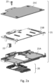
- a memory card connector 20 is constructed independently of a body of the memory card reader 21.
- the memory card connector 20 is designed to allow reading of the signals emanating from the memory card (not shown).
- the memory card connector 20 includes a certain number of pins (eight on the figure 2a ), allowing contact with corresponding areas of the memory card chip (usually six or eight areas, depending on the type of memory card). These pins are generally metal spring blades which are positioned on the surface of the chip.
- the memory card connector 20 is also intended to be connected to a main printed circuit (not shown), typically the motherboard of the reading terminal within which it is installed, in order to ensure the operation of the reader and its interconnection.
- this main printed circuit on which the connector 20 is for example soldered, is referred to as a "motherboard", in order to avoid any confusion with the printed circuit of the memory card reader body. according to the proposed technique, which covers the top cover. It should be noted, however, that the term “motherboard” should not be understood in a restrictive sense, and that in certain embodiments the main printed circuit is not necessarily the motherboard of the reading terminal. The object of the disclosure not being the memory card connector, its detailed description will not be carried out further.
- the memory card connector 20 is independent of the body of the memory card reader 21. In other words, the memory card connector 20 is not assembled with the body of the memory card reader 21 before be assembled to the motherboard of the reading terminal: according to the proposed technique, the memory card connector 20 is first fixed on the motherboard, then the body of the memory card reader 21 is assembled over the connector 20.
- the body of the memory card reader 21 itself comprises three main parts: a lower base 21A, an upper cover 21B, and a printed circuit 21C, called printed circuit, which surmounts the upper cover 21B.
- the lower base 21A includes a housing for receiving the memory card connector 20. This housing takes the form of an orifice passing through the lower base 21A right through, and in which the connector 20 is housed when the lower base 21A is positioned on the motherboard.
- the memory card connector 20 is first fixed to the motherboard, then the lower base 21A of the body of the memory card reader is positioned on the motherboard secondly, around the previously installed connector.
- the upper cover 21B is then assembled on the lower base 21A, so as to form the slot for inserting a memory card into the reader.
- the printed circuit 21C is fixed on the upper face of the upper cover, so as to cover a major part of it, ideally all of it.
- the block formed by the upper cover 21B and the printed circuit 21C may have been pre-assembled, before the assembly phase of the memory card reader. In this case, it is this entire pre-assembled block which is positioned on the lower base 21A when mounting the reader.
- the printed circuit 21C comprises at least one protection element, which is for example in the form of one or more intrusion detection lattices or in the form of one or more continuous intrusion detection tracks (for example a ground circuit, and two trellises at different potentials).
- This or these protective elements are positioned so as to cover a major part of the surface of the printed circuit 21C. Ideally, they are distributed over the entire surface of the printed circuit 21C, so as to ensure increased security of the memory card reader.
- This three-part architecture of the body of the memory card reader 21 has numerous advantages over the solutions of the prior art.
- the coupling between a top cover and a printed circuit makes it possible to obtain an interesting compromise between the level of security of the reader once assembled on the one hand, and the complexity and cost of production of the parts composing it on the other hand, in particular when this solution is compared to previous complex solutions based on the production of MID parts using LDS techniques for example.
- the printed circuit can take the form of a classic printed circuit on an epoxy support, the robustness of which is reinforced by the thickness of the upper cover on which it is fixed.
- the top cover is made of metal.
- it has increased mechanical resistance compared to traditional solutions based on plastic materials, while offering the advantage of being able to be produced on a large scale and at lower cost thanks to the implementation of known cutting techniques. and embossing metal plates for example.
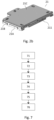
- FIG 2b shows an example of a memory card reader body according to the proposed technique, once assembled.
- the body of the memory card reader 21 is a piece of generally rectangular parallelepiped shape, with a width of approximately fifty-five millimeters, and a depth of approximately thirty-two millimeters (excluding the zone connection of the Zebra type elastomer connector, which will be presented later) and with a height of approximately four millimeters.
- this body 21 comprises a lower base 21A and an upper cover 21B.
- the lower base 21A and the upper cover 21B have complementary assembly means.
- the lower base 21A and the upper cover 21B together form an insertion slot 211 which allows a memory card to be inserted in a correct position so that it comes into contact with the memory card connector, once in stop position.
- This insertion slot has a height between 0.85 and 1.20 millimeters.
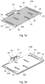
- the upper cover 21B of the body of the memory card reader 21 is presented in more detail in relation to the figures 3a and 3b , respectively in a perspective view from above and below.
- the upper cover 21B has a generally rectangular parallelepiped shape, with a generally flat and rectangular main surface 30 and two side walls (31A, 31B).
- the side walls are substantially perpendicular to the main surface 30, and include means of assembly with a lower base described later. These assembly means can for example take the form of assembly tabs 32.
- the main surface of the upper cover 21B comprises an upper face 30S and a lower face 301. Part of the lower face 301 of the upper cover 21B acts as a upper wall of the memory card insertion slot, once the body of the memory card reader is assembled.
- the upper face 30S serves as a receiving surface for fixing a printed circuit 21C, said printed circuit comprising at least one protective element.
- this printed circuit 21C is rigid and rests for example on an epoxy type support.
- the upper cover 21B is metallic. Its shape can then, for example, be obtained very simply from a simple metal plate, using usual cutting and embossing techniques.
- the side walls (31A, 31B) and the assembly tabs 32 can for example be obtained by simply folding such a previously cut metal plate.
- the upper cover 21B is embossed so as to present bumps 33 which form a set of protuberances on its upper face 30S (only a few bumps are referenced on the figure 3a , so as not to overload the figure).
- These bumps 33 have several functions. They serve primarily as support surfaces for the printed circuit 21C. They allow in particular an elevation of the printed circuit 21, which promotes the sliding of a memory card in the reader by preventing any friction of the memory card against the printed circuit 21C. The height of these bumps 33 is also dimensioned such that the printed circuit 21C is sufficiently raised to provide a reception housing of sufficient size for the connector 20.
- the cover upper 21B comprises an orifice 34 allowing the passage of a so-called counter-support zone of the memory card connector 20, when the reader is assembled.
- the printed circuit 21C must therefore be sufficiently raised to allow sufficient space to be reserved for the reception of this counter-support zone of the connector 20.
- the Figure 4 which presents an example of a memory card connector 20 according to the proposed technique, shows such a counter-support zone 41: it corresponds to a part of the connector 20 which aims to protect the card presence detection switch.
- This counter-support zone fulfills two functions. The first function is to allow adaptation to the thickness of the card. Indeed, the assembly as proposed results in a certain tolerance as to the height of the memory card reader body in relation to the memory card connector.
- This counter-support zone makes it possible to manage this slight difference in height by ensuring that the card will not be deflected when it is introduced.
- the second function is to detect the complete insertion of the card (switch system). This second function is for example fulfilled by the use of a metal leaf spring included in the counter-support zone 41.
- the orifice 34 arranged in the upper cover 21B allows the passage of the upper part of the counter-support zone 41 of connector 20, which makes it possible to obtain a memory card reader compact (the thickness of the upper cover is not added to that of the connector, to the extent that the aforementioned orifice 34 forms a housing for accommodating part of the thickest zone of the connector, namely the counter-support zone 41), without sacrificing security (the whole is still covered by the printed circuit).
- the bumps 33 present on the upper cover 21B can also serve as fixing surfaces for the printed circuit on the upper cover. Different embodiments are then possible to ensure this fixation.
- the printed circuit 21C can in particular be soldered to the upper cover 21B at the level of these bumps 33, for example by means of a SMT reflow soldering technique (“Surface Mounted Components).
- SMT reflow soldering technique Surface Mounted Components
- ground solder pads are necessary.
- fixing can be ensured by the use of a double-sided adhesive, located at the level of the bumps 33 or on the entire main surface of the upper cover 21B. In this case, it is no longer necessary to provide specific routings on the printed circuit 21C.
- Other modes of fixing the printed circuit on the upper cover are also provided within the framework of the proposed technique, in a complementary or alternative manner to fixing at the level of the bumps 33.
- the upper cover comprises at least one metal strip 35 extending substantially perpendicular to its main surface 30, on the side of its upper face 30S. These metal strips 35 were for example formed during the embossing of the upper cover 21B, when the latter is made of metal. They have a height greater than that of the bumps 33.
- the printed circuit 21C comprises through metallized holes (or vias), which are shaped and dimensioned so that each of them is able to accommodate a corresponding metal strip 35 of the upper cover 21B.
- the fixing of the printed circuit to the upper cover is then ensured by means of soldering of the through-component soldering type.
- the shape and location of the holes may have been planned so as to prevent incorrect mounting of the printed circuit on the top cover (they then act not only as keyers, but also as centering points which will ensure correct positioning of the printed circuit so as to ensure a reliable connection of this printed circuit with the motherboard in particular when such a connection is provided by a Zebra type elastomer connector).
- Such metallized holes 38 are for example visible on the figure 3c , which shows the printed circuit 21C once installed on the upper cover 21B.
- These different means of fixing the printed circuit on the upper cover are given by way of illustration and not limitation, and other means of fixing, for example based on the use of glue, screws, or even a crosslinking polymer , are also possible.
- assembly screws of the memory card reader can also be embedded in the printed circuit 21C, always with the aim of compactness.
- the bumps 33 of the upper cover also have a reinforcing role: due to their generally rectilinear shape and their distribution over the entire main surface 30 of the upper cover, they reinforce the robustness of the upper cover 21B. As a result, the latter is more resistant to folding, for example. Furthermore, the fixing of a metal part (i.e. the upper cover 21B thus honeycombed by the presence of these bumps 33) on the printed circuit 21C (generally in epoxy, i.e. thin and relatively fragile) makes it possible to add significant rigidity to the entire body of the memory card reader.
- the printed circuit 21C comprises at least one protection element.
- this protective element (or the plurality of protective elements) extends substantially over the entire surface of the printed circuit, and the printed circuit 21C is shaped and dimensioned so that once fixed on the cover upper 21B of the reader body, it covers the entire upper surface, or at least a major part. In this way, the surface covered by the protective element is large and makes it possible to secure the body of the memory card reader effectively.
- the mechanical resistance of the top cover particularly when it is made of metal, contributes to further strengthening this security.
- the use of a conventional printed circuit turns out to be less expensive and simpler to implement than other techniques of the prior art, such as that consisting for example of using MID and LDS technologies to directly trace a protective element (for example taking the form of a circuit) within the upper cover of the body of the memory card reader.
- the proposed solution therefore offers an interesting compromise, because it guarantees a significant level of security while being less complex and less costly to implement than the solutions of the art. prior.
- the printed circuit 21C also offers a usable surface for the integration, in addition to the protection element(s), of other tracks and components useful for ensuring various other ancillary functions.
- the presence of the bumps 33 on the upper cover 21B may also be of interest in the sense that the elevation of the printed circuit obtained also makes it possible to use the internal face of this circuit (that which faces the upper face 30S top cover) for installing various electronic components.
- the protective element is in the form of electrical tracks which form at least one protective mesh.
- a “high density” zone corresponds to immediate protection (direct drilling above the connector for access to sensitive signals).
- a “lower density” zone corresponds to protection against indirect attacks (drilling, then introduction of objects at an angle to access sensitive signals, as described previously).
- Such a solution is advantageous because it makes it possible to reduce the cost of manufacturing the printed circuit without compromising safety.
- the lower density zone then lends itself more particularly to the possible integration of tracks and components making it possible to carry out the possible additional functions previously mentioned.
- passive baffles we mean here shapes which make it possible to complicate, inside the assembled memory card reader, access to the areas where such sensitive signals pass. These are therefore passive security devices, which complement active protection by mesh for example. The objective of these forms is, for example, to make any attempt to introduce a tool aimed at accessing such sensitive areas more difficult.
- passive baffles can be implemented in different ways.
- the upper cover comprises passive baffles, which take the form of metal tabs (36, 37) obtained for example very simply during the cutting and embossing carried out to form the cover superior in question.
- metal tabs are for example visible on the figure 3b .
- These metal tabs (36, 37) extend substantially perpendicular to the lower face 30I of the upper cover 21B. They are shaped and sized to act as a physical shield around areas where certain sensitive signals pass. They are for example positioned around areas presenting a relative weakness in terms of security, such as for example the areas of orifices present in the upper cover 21B.
- the height of these metal tabs (36, 37) can be variable, depending on whether the sensitive signals to be protected are located in rather low or high layers of the reader.
- the passive baffles 37 aim to protect a “high” zone close to the printed circuit
- the passive baffles 36 aim to protect a “low” zone close to the motherboard, where the memory card connector is soldered.
- the metal tabs 36 are, for example, positioned as close as possible to the components of the motherboard, so as to reinforce their protection.
- the metal tabs 37 are for their part arranged around an elastomer connector (of the Zebra type for example) through which the signals supplying the printed circuit 21C pass: false contact between these tabs 37 and a protection element of the printed circuit 21C results in therefore intrusion detection.
- passive baffles can be implemented, in addition to or alternatively to the passive baffles formed on the metal upper cover 21B.
- These additional passive baffles take the form of metal pieces (an example of which is given in relation to the Figure 5 ) soldered flat to the motherboard (or at various sensitive locations on the memory card reader) thus creating robust obstacles that are difficult to circumvent when attempting to access sensitive signals.
- the upper cover 21B comprises a so-called “landing card” mechanism (sometimes also known in the literature under the name of “landing contacts”) which has the advantage of minimizing wear of the contacts. of the memory card and the metal blades of the connector during multiple insertions and removals of memory cards in the reader.
- the card landing mechanism comprises a movable counter-support 39
- the upper cover comprises a housing reception of said movable counter-support 39.
- the counter-support 39 is movable between two positions: a so-called reading position, and a so-called waiting position.
- the reading position corresponds to a position in which the movable counter-support 39 exerts pressure on a memory card inserted in the insertion slot of the memory card reader.
- This position is the reading position of a memory card by the reader. The pressure is exerted in the direction of the connector, when the memory card is inserted completely (in other words up to a stop point) in the insertion slot of the memory card reader. This position ensures reliable contact between the card contacts and the metal strips of the connector.
- the waiting position corresponds to a position in which the movable counter-support 39 is at least partially arranged in its receiving housing within the upper cover. This position is occupied by the movable counter-support 39 when no memory card is inserted in the reader, or when a card is only partially inserted there (in other words, the stop point of the card is not has not yet been achieved).
- the movable counter-support then exerts no pressure on the card, or a very low pressure which limits or does not allow contact between the contacts of the card and the metal strips of the connector.
- the housing for receiving the movable counter-support 39 can take the form of an orifice in the upper cover 21B. Once fixed, the printed circuit 21C then plays the role of cover or “roof” for this reception housing, by covering and therefore protecting this orifice. In this way, the memory card reader remains compact without sacrificing security.
- the upper cover 21B is not perforated, and the movable counter-support 39 is placed against the lower wall of the upper cover or in a recess provided in the upper cover, in its waiting position. Such an implementation is more robust, but requires increased thickness of the upper cover and therefore of the memory card reader.
- the card landing function is known per se, its implementation in the context of this embodiment therefore differs from the solutions of the prior art in which the card landing mechanism generally constitutes a point of weakness for security of the reader. Indeed, with the proposed technique, the 21C printed circuit completely protects the card landing mechanism by covering it completely.
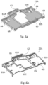
- the lower base 21A of the body of the memory card reader 21 is presented in more detail in relation to the figures 6a and 6b , respectively in a perspective view from above and below, in a particular embodiment of the proposed technique.
- the lower base 21A is generally rectangular parallelepiped in shape. It also includes a main surface 60, two side walls (61A, 61B) and two generally longitudinal walls (61C, 61D).
- the upper face 60S of the main surface 60 is the face in contact with the memory card when it is inserted into the reader: this upper face 60S is therefore generally smooth.
- the lower face 60I is the face which is in contact with the motherboard to which the card reader connector is connected.
- This lower face 60I is structured in order to accommodate in particular electronic components which are soldered to the motherboard and which the lower base 21A covers, thus ensuring a certain physical protection of these components.
- the height of the side walls (61A, 61B) and longitudinal walls (61C, 61D) is adapted to the height of the electronic components which take place under the lower base 21A.
- the lower base 21A also includes a housing intended to receive the memory card connector when mounting the memory card reader.
- This housing takes the form of an orifice 62 passing through the lower base 21A right through.
- the shape of this receiving housing 62 is substantially complementary to the shape of the memory card connector 20.
- the lower base 21A comprises centering pins 65, making it possible to ensure correct centering of the base lower on the connector 20 during assembly (the memory card connector 20 then includes complementary holes 42, visible on the Figure 4 , intended to accommodate these centering pins 65 of the lower base).
- the assembly formed by the connector 20 surrounded by the lower base 21A will subsequently be covered by the upper cover 21B, in order to form an insertion slot presenting the space necessary for the presence of a memory card, as well as 'to possible other electronic components.
- the side walls (61A, 61B) of the lower base 21A comprise passages 64 intended to accommodate complementary assembly lugs of the upper cover 21B (the assembly lugs 32 of the figures 3a and 3b ).
- assembly tabs when they are metallic, can further be soldered onto the motherboard to further enhance the robustness of the assembled drive.
- Other embodiments than that illustrated are obviously possible for assembling the upper cover 21B on the lower base 21A.
- the connection between the printed circuit and the motherboard is made via an elastomer connector, for example of the Zebra type (registered trademark).
- an elastomer connector for example of the Zebra type (registered trademark).
- the connection is ensured via an elastomer connector, the assembly of the memory card connector, elastomer connector and memory card reader body assembly is facilitated.
- the exploded view of the figure 2a shows such an elastomeric connector 22 and the way in which it can be implemented in a particular embodiment. More particularly, the lower base 21A and the upper cover 21B each include an orifice allowing the installation of the elastomeric connector 22 during assembly of the reader.
- steps 74 and 75 are replaced by a single step of assembling, on the lower base, the pre-assembled block formed by the upper cover surmounted by the printed circuit.
Landscapes
- Engineering & Computer Science (AREA)
- Theoretical Computer Science (AREA)
- Physics & Mathematics (AREA)
- General Physics & Mathematics (AREA)
- Artificial Intelligence (AREA)
- Computer Vision & Pattern Recognition (AREA)
- Computer Hardware Design (AREA)
- Computer Security & Cryptography (AREA)
- Software Systems (AREA)
- General Engineering & Computer Science (AREA)
- Coupling Device And Connection With Printed Circuit (AREA)
- Credit Cards Or The Like (AREA)
Claims (13)
- Körper eines Lesegeräts für Speicherkarten (21) von insgesamt rechteckiger parallelepipedischer Form, der einen Schlitz zum Einführen (211) einer Speicherkarte und ein Gehäuse für die Aufnahme eines Steckers für die Speicherkarte (20) umfasst, wobei der Lesegerätkörper (21) eine obere Abdeckung (21B) und eine untere Basis (21A) umfasst,wobei der Einführungsschlitz durch das Zusammenfügen der oberen Abdeckung (21B) und der unteren Basis (21A) gebildet wird, wobei das Aufnahmegehäuse die Form einer Öffnung annimmt, die durch die untere Basis (21A) von einer Seite zur anderen hindurchgeht, wobei der Speicherkartenlesegerätkörper dadurch gekennzeichnet ist, dass die obere Abdeckung (21B) aus Metall besteht und ferner eine Leiterplatte (21C) umfasst, die an einer Oberseite der oberen Abdeckung (21B) befestigt ist,wobei die Leiterplatte (21C) mindestens ein Schutzelement umfasst, das in Form eines oder mehrerer Drahtgeflechte zur Intrusionserkennung vorliegt oder in Form einer oder mehrerer kontinuierlicher Bahnen zur Intrusionserkennung.
- Speicherkartenlesegerätkörper nach Anspruch 1, dadurch gekennzeichnet, dass die Leiterplatte (21C) einen Großteil der Oberseite der oberen Abdeckung (21B) bedeckt.
- Speicherkartenlesegerätkörper nach Anspruch 1, dadurch gekennzeichnet, dass sich das Schutzelement im Wesentlichen über einen Großteil der Leiterplatte (21C) erstreckt.
- Speicherkartenlesegerätkörper nach Anspruch 1, dadurch gekennzeichnet, dass die Ätzdichte des Schutzelements in Abhängigkeit von der Lage des Schutzelements variabel ist.
- Speicherkartenlesegerätkörper nach Anspruch 1, dadurch gekennzeichnet, dass die obere Abdeckung (21B) mindestens eine Einbeulung (33) umfasst, die sich im Wesentlichen senkrecht zur Oberseite der oberen Abdeckung erstreckt.
- Speicherkartenlesegerätkörper nach Anspruch 1, dadurch gekennzeichnet, dass die obere Abdeckung (21B) in der Nähe einer Öffnung, die durch die obere Abdeckung hindurchgeht, mindestens eine Metalllasche (36, 37) umfasst, die sich im Wesentlichen senkrecht zu einer Unterseite der oberen Abdeckung erstreckt.
- Speicherkartenlesegerätkörper nach Anspruch 1, dadurch gekennzeichnet, dass die obere Abdeckung (21B) mindestens einen Kartenankunftsmechanismus umfasst.
- Speicherkartenlesegerätkörper nach Anspruch 7, dadurch gekennzeichnet, dass der Kartenankunftsmechanismus ein bewegliches Gegenlager (39) umfasst, und dass die obere Abdeckung (21B) ein Aufnahmegehäuse für das bewegliche Gegenlager umfasst, wobei das bewegliche Gegenlager zwischen zwei Positionen beweglich ist:- einer Leseposition, in der das bewegliche Gegenlager Druck auf eine Speicherkarte ausübt, die in den Einführungsschlitz des Speicherkartenlesegeräts eingeführt ist;- einer Warteposition, in der das bewegliche Gegenlager mindestens teilweise im Aufnahmegehäuse angeordnet ist.
- Speicherkartenlesegerätkörper nach Anspruch 8, dadurch gekennzeichnet, dass das Aufnahmegehäuse des beweglichen Gegenlagers (39) die Form einer Öffnung innerhalb der oberen Abdeckung (21B) annimmt.
- Speicherkartenlesegerätkörper nach Anspruch 1, dadurch gekennzeichnet, dass die untere Basis (21A) mindestens eine Kartenbremsvorrichtung (63A, 63B) umfasst.
- Speicherkartenlesegerätkörper nach Anspruch 1, dadurch gekennzeichnet, dass die untere Basis (21A) mindestens eine elektrostatische Entladungszone umfasst.
- Speicherkartenleseterminal, dadurch gekennzeichnet, dass es einen Speicherkartenlesegerätkörper nach einem der Ansprüche 1 bis 11 umfasst.
- Verfahren zum Zusammenfügen eines Speicherkartenlesegerätkörpers nach einem der Ansprüche 1 bis 11, dadurch gekennzeichnet, dass es umfasst:- einen Schritt zum Befestigen (71) eines Speicherkartensteckers (20) an einer Grundplatine;- einen Schritt zum Einbauen (73) der unteren Basis (21A) auf dem Speicherkartenstecker (20);- einen Schritt (74) zum Zusammenfügen der oberen Abdeckung (21B) mit der unteren Basis (21A);- einen Schritt zum Befestigen (75) der Leiterplatte (21C) auf der Oberseite der oberen Abdeckung (21B).
Applications Claiming Priority (1)
| Application Number | Priority Date | Filing Date | Title |
|---|---|---|---|
| FR1750301A FR3061972B1 (fr) | 2017-01-13 | 2017-01-13 | Corps de lecteur de cartes a memoire securise |
Publications (2)
| Publication Number | Publication Date |
|---|---|
| EP3349139A1 EP3349139A1 (de) | 2018-07-18 |
| EP3349139B1 true EP3349139B1 (de) | 2024-08-07 |
Family
ID=58547657
Family Applications (1)
| Application Number | Title | Priority Date | Filing Date |
|---|---|---|---|
| EP18150857.3A Active EP3349139B1 (de) | 2017-01-13 | 2018-01-09 | Körper eines kartenlesegeräts mit gesichertem speicher |
Country Status (5)
| Country | Link |
|---|---|
| US (1) | US10312625B2 (de) |
| EP (1) | EP3349139B1 (de) |
| CA (1) | CA2991551C (de) |
| ES (1) | ES2990261T3 (de) |
| FR (1) | FR3061972B1 (de) |
Families Citing this family (10)
| Publication number | Priority date | Publication date | Assignee | Title |
|---|---|---|---|---|
| FR3088469B1 (fr) * | 2018-11-08 | 2023-01-06 | Ingenico Group | Support d'indicateur visuel et dispositif de paiement correspondant |
| CN209168118U (zh) * | 2018-12-12 | 2019-07-26 | 百富计算机技术(深圳)有限公司 | 读卡器及pos机 |
| FR3097669B1 (fr) * | 2019-06-20 | 2021-12-10 | Ingenico Group | système de lecture de carte de transaction hybride |
| JP6712793B1 (ja) * | 2020-02-13 | 2020-06-24 | パナソニックIpマネジメント株式会社 | 情報処理装置、及び、情報処理装置の製造方法 |
| US11818842B1 (en) * | 2020-03-06 | 2023-11-14 | Amazon Technologies, Inc. | Configurable circuit board for abstracting third-party controls |
| US11201423B2 (en) * | 2020-07-15 | 2021-12-14 | Google Llc | Card connector assemblies with integrated component shielding |
| US12431939B2 (en) * | 2022-06-06 | 2025-09-30 | Ingenutec, LLC | Near field communication module |
| US12217107B2 (en) | 2023-01-25 | 2025-02-04 | Google Llc | Integrated memory card ejector and sensor ports |
| JP2024164956A (ja) * | 2023-05-16 | 2024-11-28 | ニデックインスツルメンツ株式会社 | 情報処理装置 |
| FR3164304A1 (fr) * | 2024-07-04 | 2026-01-09 | Banks And Acquirers International Holding | terminal électronique et système de sécurité |
Family Cites Families (28)
| Publication number | Priority date | Publication date | Assignee | Title |
|---|---|---|---|---|
| US5233505A (en) * | 1991-12-30 | 1993-08-03 | Yeng-Ming Chang | Security device for protecting electronically-stored data |
| TW507950U (en) * | 2001-12-26 | 2002-10-21 | Hon Hai Prec Ind Co Ltd | Electronic card connector |
| US6853093B2 (en) * | 2002-12-20 | 2005-02-08 | Lipman Electronic Engineering Ltd. | Anti-tampering enclosure for electronic circuitry |
| US7180008B2 (en) * | 2004-01-23 | 2007-02-20 | Pitney Bowes Inc. | Tamper barrier for electronic device |
| US7015823B1 (en) * | 2004-10-15 | 2006-03-21 | Systran Federal Corporation | Tamper resistant circuit boards |
| TWM280565U (en) * | 2005-03-11 | 2005-11-11 | Hon Hai Prec Ind Co Ltd | Electrical card connector |
| FR2889756B1 (fr) * | 2005-08-11 | 2007-10-12 | Itt Mfg Enterprises Inc | Agencement de securite contre la fraude pour connecteur electrique pour carte a puce |
| US20070177363A1 (en) * | 2006-01-31 | 2007-08-02 | Symbol Technologies, Inc. | Multilayer printed circuit board having tamper detection circuitry |
| FR2906623B1 (fr) * | 2006-10-02 | 2009-01-16 | Sagem Monetel Soc Par Actions | Dispositif de protection pour carte electronique |
| TWI351140B (en) * | 2006-10-30 | 2011-10-21 | Hon Hai Prec Ind Co Ltd | Electrical card connector |
| TW200824190A (en) * | 2006-11-20 | 2008-06-01 | Hon Hai Prec Ind Co Ltd | Electrical card connector |
| TWM320206U (en) * | 2007-02-05 | 2007-10-01 | Hon Hai Prec Ind Co Ltd | Electrical card connector |
| TWM323131U (en) * | 2007-04-23 | 2007-12-01 | Hon Hai Prec Ind Co Ltd | Electrical card connector |
| TWI358161B (en) * | 2007-07-24 | 2012-02-11 | Hon Hai Prec Ind Co Ltd | Electrical card connector |
| CN100576985C (zh) * | 2007-09-21 | 2009-12-30 | 百富计算机技术(深圳)有限公司 | 安全保护盖 |
| CN100464340C (zh) * | 2007-09-21 | 2009-02-25 | 百富计算机技术(深圳)有限公司 | 安全保护盒 |
| US9013336B2 (en) * | 2008-01-22 | 2015-04-21 | Verifone, Inc. | Secured keypad devices |
| FR2934110B1 (fr) * | 2008-07-16 | 2010-10-22 | Ingenico Sa | Dispositif de protection d'un composant electronique. |
| CN201266693Y (zh) * | 2008-08-31 | 2009-07-01 | 富士康(昆山)电脑接插件有限公司 | 电连接器 |
| FR2944625B1 (fr) * | 2009-04-15 | 2012-03-09 | Ingenico Sa | Lecteur de carte memoire. |
| TWM402516U (en) * | 2010-09-30 | 2011-04-21 | Hon Hai Prec Ind Co Ltd | Electrical connector |
| US8593824B2 (en) * | 2010-10-27 | 2013-11-26 | Verifone, Inc. | Tamper secure circuitry especially for point of sale terminal |
| US20130140364A1 (en) * | 2011-12-01 | 2013-06-06 | Magtek, Inc. | Systems and methods for detecting and preventing tampering of card readers |
| FR2983995A1 (fr) * | 2011-12-12 | 2013-06-14 | Ingenico Sa | Dispositif de decharge electrostatique |
| US9450586B2 (en) * | 2012-10-02 | 2016-09-20 | Hewlett Packard Enterprise Development Lp | Security shield assembly |
| FR2997530B1 (fr) | 2012-10-30 | 2016-12-23 | Cie Ind Et Financiere D'ingenierie Ingenico | Corps de lecteur de carte a memoire securise |
| FR2997570B1 (fr) * | 2012-10-30 | 2016-01-08 | Ingenico Sa | Connecteur de carte a memoire securise. |
| FR3012720B1 (fr) * | 2013-10-31 | 2016-01-01 | Ingenico Sa | Procede de fabrication d'un corps de lecteur de carte a memoire, corps de lecteur de carte a memoire et terminal de lecture de carte a memoire correspondants |
-
2017
- 2017-01-13 FR FR1750301A patent/FR3061972B1/fr active Active
-
2018
- 2018-01-09 ES ES18150857T patent/ES2990261T3/es active Active
- 2018-01-09 EP EP18150857.3A patent/EP3349139B1/de active Active
- 2018-01-11 CA CA2991551A patent/CA2991551C/fr active Active
- 2018-01-15 US US15/871,606 patent/US10312625B2/en active Active
Also Published As
| Publication number | Publication date |
|---|---|
| FR3061972A1 (fr) | 2018-07-20 |
| EP3349139A1 (de) | 2018-07-18 |
| CA2991551A1 (fr) | 2018-07-13 |
| ES2990261T3 (es) | 2024-11-29 |
| US20180205170A1 (en) | 2018-07-19 |
| US10312625B2 (en) | 2019-06-04 |
| CA2991551C (fr) | 2026-04-14 |
| FR3061972B1 (fr) | 2020-02-14 |
Similar Documents
| Publication | Publication Date | Title |
|---|---|---|
| EP3349139B1 (de) | Körper eines kartenlesegeräts mit gesichertem speicher | |
| FR2830107A1 (fr) | Cle electronique destinee a etre connectee a un port d'un dispositif de telecommunication et procede de fabrication de la cle | |
| EP0647918A1 (de) | Tragbare Mehrzweckkarte für Personalrechner | |
| EP2915094B1 (de) | Kartenleserkörper mit gesicherten speicher | |
| EP3371735B1 (de) | Körper eines speicherkartenlesers mit einem schutznetz auf beiden seiten | |
| EP3326108B1 (de) | Kompaktkartenleser | |
| EP2791859B1 (de) | Elektrostatische entladevorrichtung | |
| WO2015062982A1 (fr) | Procédé de fabrication d'un corps de lecteur de carte à mémoire, corps de lecteur de carte à mémoire et terminal de lecture de carte à mémoire correspondants | |
| EP2915093B1 (de) | Sicherer verbinder für eine speicherkarte | |
| EP3252652B1 (de) | Körper eines kartenlesegeräts mit gesichertem speicher | |
| EP4237988B1 (de) | Lötbarer chipkartenverbinder und entsprechendes montageverfahren | |
| EP3063697B1 (de) | Speicherkartenleseanordnung inklusive intrusionsschutz | |
| EP3295365B1 (de) | Erkennung der öffnung einer dateneingabevorrichtung | |
| FR3085514A1 (fr) | Terminal de lecture de carte a memoire comprenant un moyen de compensation d'inclinaison | |
| FR2985154A1 (fr) | Circuit imprime flexible. | |
| EP3116070B1 (de) | Steckverbinder eines gesicherten integrierten schaltkreises | |
| EP3987431B1 (de) | Hybrides transaktionskartenlesesystem | |
| FR3038780A1 (fr) | Connecteur de circuit integre securise | |
| FR2957443A1 (fr) | Carte a microcircuit(s) avec contremesure pour attaques en faute par rayonnement lumineux |
Legal Events
| Date | Code | Title | Description |
|---|---|---|---|
| PUAI | Public reference made under article 153(3) epc to a published international application that has entered the european phase |
Free format text: ORIGINAL CODE: 0009012 |
|
| STAA | Information on the status of an ep patent application or granted ep patent |
Free format text: STATUS: THE APPLICATION HAS BEEN PUBLISHED |
|
| AK | Designated contracting states |
Kind code of ref document: A1 Designated state(s): AL AT BE BG CH CY CZ DE DK EE ES FI FR GB GR HR HU IE IS IT LI LT LU LV MC MK MT NL NO PL PT RO RS SE SI SK SM TR |
|
| AX | Request for extension of the european patent |
Extension state: BA ME |
|
| STAA | Information on the status of an ep patent application or granted ep patent |
Free format text: STATUS: REQUEST FOR EXAMINATION WAS MADE |
|
| 17P | Request for examination filed |
Effective date: 20190118 |
|
| RBV | Designated contracting states (corrected) |
Designated state(s): AL AT BE BG CH CY CZ DE DK EE ES FI FR GB GR HR HU IE IS IT LI LT LU LV MC MK MT NL NO PL PT RO RS SE SI SK SM TR |
|
| STAA | Information on the status of an ep patent application or granted ep patent |
Free format text: STATUS: EXAMINATION IS IN PROGRESS |
|
| 17Q | First examination report despatched |
Effective date: 20200213 |
|
| RAP1 | Party data changed (applicant data changed or rights of an application transferred) |
Owner name: BANKS AND ACQUIRERS INTERNATIONAL HOLDING |
|
| GRAP | Despatch of communication of intention to grant a patent |
Free format text: ORIGINAL CODE: EPIDOSNIGR1 |
|
| STAA | Information on the status of an ep patent application or granted ep patent |
Free format text: STATUS: GRANT OF PATENT IS INTENDED |
|
| INTG | Intention to grant announced |
Effective date: 20240326 |
|
| GRAS | Grant fee paid |
Free format text: ORIGINAL CODE: EPIDOSNIGR3 |
|
| GRAA | (expected) grant |
Free format text: ORIGINAL CODE: 0009210 |
|
| STAA | Information on the status of an ep patent application or granted ep patent |
Free format text: STATUS: THE PATENT HAS BEEN GRANTED |
|
| AK | Designated contracting states |
Kind code of ref document: B1 Designated state(s): AL AT BE BG CH CY CZ DE DK EE ES FI FR GB GR HR HU IE IS IT LI LT LU LV MC MK MT NL NO PL PT RO RS SE SI SK SM TR |
|
| REG | Reference to a national code |
Ref country code: GB Ref legal event code: FG4D Free format text: NOT ENGLISH |
|
| REG | Reference to a national code |
Ref country code: CH Ref legal event code: EP |
|
| REG | Reference to a national code |
Ref country code: IE Ref legal event code: FG4D Free format text: LANGUAGE OF EP DOCUMENT: FRENCH |
|
| REG | Reference to a national code |
Ref country code: DE Ref legal event code: R096 Ref document number: 602018072663 Country of ref document: DE |
|
| REG | Reference to a national code |
Ref country code: LT Ref legal event code: MG9D |
|
| REG | Reference to a national code |
Ref country code: ES Ref legal event code: FG2A Ref document number: 2990261 Country of ref document: ES Kind code of ref document: T3 Effective date: 20241129 |
|
| REG | Reference to a national code |
Ref country code: NL Ref legal event code: MP Effective date: 20240807 |
|
| PG25 | Lapsed in a contracting state [announced via postgrant information from national office to epo] |
Ref country code: NO Free format text: LAPSE BECAUSE OF FAILURE TO SUBMIT A TRANSLATION OF THE DESCRIPTION OR TO PAY THE FEE WITHIN THE PRESCRIBED TIME-LIMIT Effective date: 20241107 |
|
| REG | Reference to a national code |
Ref country code: AT Ref legal event code: MK05 Ref document number: 1711741 Country of ref document: AT Kind code of ref document: T Effective date: 20240807 |
|
| PG25 | Lapsed in a contracting state [announced via postgrant information from national office to epo] |
Ref country code: FI Free format text: LAPSE BECAUSE OF FAILURE TO SUBMIT A TRANSLATION OF THE DESCRIPTION OR TO PAY THE FEE WITHIN THE PRESCRIBED TIME-LIMIT Effective date: 20240807 Ref country code: NL Free format text: LAPSE BECAUSE OF FAILURE TO SUBMIT A TRANSLATION OF THE DESCRIPTION OR TO PAY THE FEE WITHIN THE PRESCRIBED TIME-LIMIT Effective date: 20240807 Ref country code: GR Free format text: LAPSE BECAUSE OF FAILURE TO SUBMIT A TRANSLATION OF THE DESCRIPTION OR TO PAY THE FEE WITHIN THE PRESCRIBED TIME-LIMIT Effective date: 20241108 Ref country code: PL Free format text: LAPSE BECAUSE OF FAILURE TO SUBMIT A TRANSLATION OF THE DESCRIPTION OR TO PAY THE FEE WITHIN THE PRESCRIBED TIME-LIMIT Effective date: 20240807 Ref country code: PT Free format text: LAPSE BECAUSE OF FAILURE TO SUBMIT A TRANSLATION OF THE DESCRIPTION OR TO PAY THE FEE WITHIN THE PRESCRIBED TIME-LIMIT Effective date: 20241209 |
|
| PG25 | Lapsed in a contracting state [announced via postgrant information from national office to epo] |
Ref country code: BG Free format text: LAPSE BECAUSE OF FAILURE TO SUBMIT A TRANSLATION OF THE DESCRIPTION OR TO PAY THE FEE WITHIN THE PRESCRIBED TIME-LIMIT Effective date: 20240807 |
|
| PG25 | Lapsed in a contracting state [announced via postgrant information from national office to epo] |
Ref country code: LV Free format text: LAPSE BECAUSE OF FAILURE TO SUBMIT A TRANSLATION OF THE DESCRIPTION OR TO PAY THE FEE WITHIN THE PRESCRIBED TIME-LIMIT Effective date: 20240807 |
|
| PG25 | Lapsed in a contracting state [announced via postgrant information from national office to epo] |
Ref country code: AT Free format text: LAPSE BECAUSE OF FAILURE TO SUBMIT A TRANSLATION OF THE DESCRIPTION OR TO PAY THE FEE WITHIN THE PRESCRIBED TIME-LIMIT Effective date: 20240807 Ref country code: IS Free format text: LAPSE BECAUSE OF FAILURE TO SUBMIT A TRANSLATION OF THE DESCRIPTION OR TO PAY THE FEE WITHIN THE PRESCRIBED TIME-LIMIT Effective date: 20241207 |
|
| PG25 | Lapsed in a contracting state [announced via postgrant information from national office to epo] |
Ref country code: HR Free format text: LAPSE BECAUSE OF FAILURE TO SUBMIT A TRANSLATION OF THE DESCRIPTION OR TO PAY THE FEE WITHIN THE PRESCRIBED TIME-LIMIT Effective date: 20240807 |
|
| PG25 | Lapsed in a contracting state [announced via postgrant information from national office to epo] |
Ref country code: RS Free format text: LAPSE BECAUSE OF FAILURE TO SUBMIT A TRANSLATION OF THE DESCRIPTION OR TO PAY THE FEE WITHIN THE PRESCRIBED TIME-LIMIT Effective date: 20241107 |
|
| PG25 | Lapsed in a contracting state [announced via postgrant information from national office to epo] |
Ref country code: RS Free format text: LAPSE BECAUSE OF FAILURE TO SUBMIT A TRANSLATION OF THE DESCRIPTION OR TO PAY THE FEE WITHIN THE PRESCRIBED TIME-LIMIT Effective date: 20241107 Ref country code: PT Free format text: LAPSE BECAUSE OF FAILURE TO SUBMIT A TRANSLATION OF THE DESCRIPTION OR TO PAY THE FEE WITHIN THE PRESCRIBED TIME-LIMIT Effective date: 20241209 Ref country code: PL Free format text: LAPSE BECAUSE OF FAILURE TO SUBMIT A TRANSLATION OF THE DESCRIPTION OR TO PAY THE FEE WITHIN THE PRESCRIBED TIME-LIMIT Effective date: 20240807 Ref country code: NO Free format text: LAPSE BECAUSE OF FAILURE TO SUBMIT A TRANSLATION OF THE DESCRIPTION OR TO PAY THE FEE WITHIN THE PRESCRIBED TIME-LIMIT Effective date: 20241107 Ref country code: NL Free format text: LAPSE BECAUSE OF FAILURE TO SUBMIT A TRANSLATION OF THE DESCRIPTION OR TO PAY THE FEE WITHIN THE PRESCRIBED TIME-LIMIT Effective date: 20240807 Ref country code: LV Free format text: LAPSE BECAUSE OF FAILURE TO SUBMIT A TRANSLATION OF THE DESCRIPTION OR TO PAY THE FEE WITHIN THE PRESCRIBED TIME-LIMIT Effective date: 20240807 Ref country code: IS Free format text: LAPSE BECAUSE OF FAILURE TO SUBMIT A TRANSLATION OF THE DESCRIPTION OR TO PAY THE FEE WITHIN THE PRESCRIBED TIME-LIMIT Effective date: 20241207 Ref country code: HR Free format text: LAPSE BECAUSE OF FAILURE TO SUBMIT A TRANSLATION OF THE DESCRIPTION OR TO PAY THE FEE WITHIN THE PRESCRIBED TIME-LIMIT Effective date: 20240807 Ref country code: GR Free format text: LAPSE BECAUSE OF FAILURE TO SUBMIT A TRANSLATION OF THE DESCRIPTION OR TO PAY THE FEE WITHIN THE PRESCRIBED TIME-LIMIT Effective date: 20241108 Ref country code: FI Free format text: LAPSE BECAUSE OF FAILURE TO SUBMIT A TRANSLATION OF THE DESCRIPTION OR TO PAY THE FEE WITHIN THE PRESCRIBED TIME-LIMIT Effective date: 20240807 Ref country code: BG Free format text: LAPSE BECAUSE OF FAILURE TO SUBMIT A TRANSLATION OF THE DESCRIPTION OR TO PAY THE FEE WITHIN THE PRESCRIBED TIME-LIMIT Effective date: 20240807 Ref country code: AT Free format text: LAPSE BECAUSE OF FAILURE TO SUBMIT A TRANSLATION OF THE DESCRIPTION OR TO PAY THE FEE WITHIN THE PRESCRIBED TIME-LIMIT Effective date: 20240807 |
|
| PG25 | Lapsed in a contracting state [announced via postgrant information from national office to epo] |
Ref country code: DK Free format text: LAPSE BECAUSE OF FAILURE TO SUBMIT A TRANSLATION OF THE DESCRIPTION OR TO PAY THE FEE WITHIN THE PRESCRIBED TIME-LIMIT Effective date: 20240807 Ref country code: RO Free format text: LAPSE BECAUSE OF FAILURE TO SUBMIT A TRANSLATION OF THE DESCRIPTION OR TO PAY THE FEE WITHIN THE PRESCRIBED TIME-LIMIT Effective date: 20240807 Ref country code: SM Free format text: LAPSE BECAUSE OF FAILURE TO SUBMIT A TRANSLATION OF THE DESCRIPTION OR TO PAY THE FEE WITHIN THE PRESCRIBED TIME-LIMIT Effective date: 20240807 |
|
| PG25 | Lapsed in a contracting state [announced via postgrant information from national office to epo] |
Ref country code: EE Free format text: LAPSE BECAUSE OF FAILURE TO SUBMIT A TRANSLATION OF THE DESCRIPTION OR TO PAY THE FEE WITHIN THE PRESCRIBED TIME-LIMIT Effective date: 20240807 |
|
| PG25 | Lapsed in a contracting state [announced via postgrant information from national office to epo] |
Ref country code: CZ Free format text: LAPSE BECAUSE OF FAILURE TO SUBMIT A TRANSLATION OF THE DESCRIPTION OR TO PAY THE FEE WITHIN THE PRESCRIBED TIME-LIMIT Effective date: 20240807 |
|
| PG25 | Lapsed in a contracting state [announced via postgrant information from national office to epo] |
Ref country code: SK Free format text: LAPSE BECAUSE OF FAILURE TO SUBMIT A TRANSLATION OF THE DESCRIPTION OR TO PAY THE FEE WITHIN THE PRESCRIBED TIME-LIMIT Effective date: 20240807 |
|
| REG | Reference to a national code |
Ref country code: DE Ref legal event code: R097 Ref document number: 602018072663 Country of ref document: DE |
|
| PLBE | No opposition filed within time limit |
Free format text: ORIGINAL CODE: 0009261 |
|
| STAA | Information on the status of an ep patent application or granted ep patent |
Free format text: STATUS: NO OPPOSITION FILED WITHIN TIME LIMIT |
|
| 26N | No opposition filed |
Effective date: 20250508 |
|
| REG | Reference to a national code |
Ref country code: CH Ref legal event code: PL |
|
| PG25 | Lapsed in a contracting state [announced via postgrant information from national office to epo] |
Ref country code: SE Free format text: LAPSE BECAUSE OF FAILURE TO SUBMIT A TRANSLATION OF THE DESCRIPTION OR TO PAY THE FEE WITHIN THE PRESCRIBED TIME-LIMIT Effective date: 20240807 |
|
| PG25 | Lapsed in a contracting state [announced via postgrant information from national office to epo] |
Ref country code: LU Free format text: LAPSE BECAUSE OF NON-PAYMENT OF DUE FEES Effective date: 20250109 Ref country code: MC Free format text: LAPSE BECAUSE OF FAILURE TO SUBMIT A TRANSLATION OF THE DESCRIPTION OR TO PAY THE FEE WITHIN THE PRESCRIBED TIME-LIMIT Effective date: 20240807 |
|
| PG25 | Lapsed in a contracting state [announced via postgrant information from national office to epo] |
Ref country code: BE Free format text: LAPSE BECAUSE OF NON-PAYMENT OF DUE FEES Effective date: 20250131 |
|
| PG25 | Lapsed in a contracting state [announced via postgrant information from national office to epo] |
Ref country code: CH Free format text: LAPSE BECAUSE OF NON-PAYMENT OF DUE FEES Effective date: 20250131 |
|
| REG | Reference to a national code |
Ref country code: BE Ref legal event code: MM Effective date: 20250131 |
|
| PG25 | Lapsed in a contracting state [announced via postgrant information from national office to epo] |
Ref country code: IE Free format text: LAPSE BECAUSE OF NON-PAYMENT OF DUE FEES Effective date: 20250109 |
|
| PG25 | Lapsed in a contracting state [announced via postgrant information from national office to epo] |
Ref country code: IT Free format text: LAPSE BECAUSE OF FAILURE TO SUBMIT A TRANSLATION OF THE DESCRIPTION OR TO PAY THE FEE WITHIN THE PRESCRIBED TIME-LIMIT Effective date: 20240807 |
|
| P01 | Opt-out of the competence of the unified patent court (upc) registered |
Free format text: CASE NUMBER: UPC_APP_0000328_3349139/2026 Effective date: 20260106 |
|
| PGFP | Annual fee paid to national office [announced via postgrant information from national office to epo] |
Ref country code: GB Payment date: 20260123 Year of fee payment: 9 |
|
| PGFP | Annual fee paid to national office [announced via postgrant information from national office to epo] |
Ref country code: ES Payment date: 20260227 Year of fee payment: 9 |
|
| PGFP | Annual fee paid to national office [announced via postgrant information from national office to epo] |
Ref country code: DE Payment date: 20260121 Year of fee payment: 9 |
|
| PGFP | Annual fee paid to national office [announced via postgrant information from national office to epo] |
Ref country code: FR Payment date: 20260129 Year of fee payment: 9 |