EP4237988B1 - Lötbarer chipkartenverbinder und entsprechendes montageverfahren - Google Patents
Lötbarer chipkartenverbinder und entsprechendes montageverfahren Download PDFInfo
- Publication number
- EP4237988B1 EP4237988B1 EP21805434.4A EP21805434A EP4237988B1 EP 4237988 B1 EP4237988 B1 EP 4237988B1 EP 21805434 A EP21805434 A EP 21805434A EP 4237988 B1 EP4237988 B1 EP 4237988B1
- Authority
- EP
- European Patent Office
- Prior art keywords
- memory card
- card reader
- motherboard
- reader body
- base
- Prior art date
- Legal status (The legal status is an assumption and is not a legal conclusion. Google has not performed a legal analysis and makes no representation as to the accuracy of the status listed.)
- Active
Links
Images



Classifications
-
- G—PHYSICS
- G06—COMPUTING OR CALCULATING; COUNTING
- G06K—GRAPHICAL DATA READING; PRESENTATION OF DATA; RECORD CARRIERS; HANDLING RECORD CARRIERS
- G06K7/00—Methods or arrangements for sensing record carriers, e.g. for reading patterns
- G06K7/0013—Methods or arrangements for sensing record carriers, e.g. for reading patterns by galvanic contacts, e.g. card connectors for ISO-7816 compliant smart cards or memory cards, e.g. SD card readers
- G06K7/0056—Methods or arrangements for sensing record carriers, e.g. for reading patterns by galvanic contacts, e.g. card connectors for ISO-7816 compliant smart cards or memory cards, e.g. SD card readers housing of the card connector
-
- H—ELECTRICITY
- H01—ELECTRIC ELEMENTS
- H01R—ELECTRICALLY-CONDUCTIVE CONNECTIONS; STRUCTURAL ASSOCIATIONS OF A PLURALITY OF MUTUALLY-INSULATED ELECTRICAL CONNECTING ELEMENTS; COUPLING DEVICES; CURRENT COLLECTORS
- H01R43/00—Apparatus or processes specially adapted for manufacturing, assembling, maintaining, or repairing of line connectors or current collectors or for joining electric conductors
- H01R43/20—Apparatus or processes specially adapted for manufacturing, assembling, maintaining, or repairing of line connectors or current collectors or for joining electric conductors for assembling or disassembling contact members with insulating base, case or sleeve
- H01R43/205—Apparatus or processes specially adapted for manufacturing, assembling, maintaining, or repairing of line connectors or current collectors or for joining electric conductors for assembling or disassembling contact members with insulating base, case or sleeve with a panel or printed circuit board
-
- G—PHYSICS
- G06—COMPUTING OR CALCULATING; COUNTING
- G06K—GRAPHICAL DATA READING; PRESENTATION OF DATA; RECORD CARRIERS; HANDLING RECORD CARRIERS
- G06K7/00—Methods or arrangements for sensing record carriers, e.g. for reading patterns
- G06K7/10—Methods or arrangements for sensing record carriers, e.g. for reading patterns by electromagnetic radiation, e.g. optical sensing; by corpuscular radiation
- G06K7/10009—Methods or arrangements for sensing record carriers, e.g. for reading patterns by electromagnetic radiation, e.g. optical sensing; by corpuscular radiation sensing by radiation using wavelengths larger than 0.1 mm, e.g. radio-waves or microwaves
- G06K7/10297—Methods or arrangements for sensing record carriers, e.g. for reading patterns by electromagnetic radiation, e.g. optical sensing; by corpuscular radiation sensing by radiation using wavelengths larger than 0.1 mm, e.g. radio-waves or microwaves arrangements for handling protocols designed for non-contact record carriers such as RFIDs NFCs, e.g. ISO/IEC 14443 and 18092
Definitions
- the invention relates to the field of memory card readers.
- the invention more particularly relates to a memory card reader intended to be mounted in a memory card reading terminal, such as a payment terminal or an identification terminal for example. More generally, the invention relates to any type of terminal that can include a memory card reader.
- Memory card reading terminals comprise, in addition to a memory card reader, a number of components such as a keyboard, a screen, one or more processors, memory, a power supply. For several years, memory card reading terminals have seen their functions multiply. This is particularly true for payment terminals. In addition to the payment function, these terminals include network communication functions, contactless memory card detection functions, coupon management functions (for example loyalty coupons), etc.
- memory card reading terminals In addition to the proliferation of these auxiliary functions, memory card reading terminals must also be resistant to the various attacks or fraud attempts to which they are frequently subject. In order to obtain uniform resistance of terminals to attacks, international standards have been issued. In the field of payment, for example, the PCI PED standard ("Payment Card Industry - Pin Entry Device") sets out requirements for intrusion and detection of attempted attacks on terminals. This is not the only standard in force.
- PCI PED Payment Card Industry - Pin Entry Device
- the memory card reader in fact, remains a weak link in the memory card reading terminal. This is due to the fact that the memory card reader includes a slot for inserting the memory card, this slot making the inside of the memory card reading terminal accessible from the outside. More specifically, attackers are seeking to gain access to the memory card connector.
- the memory card connector is the part of the memory card reader that comes into contact with the chip or the microprocessor embedded in the memory card.
- memory card readers have been provided with mesh protection. This protection prevents insertion by drilling into the terminal. When an object attempts to penetrate the protective enclosure, a short circuit is produced, causing the terminal to be disabled.
- modifications to protect the memory card connectors against electrostatic discharges and wear have also been proposed. For example, this involves having metal parts at the entrance to the memory card reader to provide mechanical guidance (prevention of wear) and/or discharge of the card prior to its insertion into the memory card reader. These metal parts are commonly in the form of metal guide rods a few millimeters high. Another example is to add metal parts in the form of a card discharge comb.
- This step of assembling and welding the body of the memory card reader is one of the many steps in assembling a memory card reading terminal carried out manually, contributing to a high manufacturing cost.
- WO 97/39418 Al discloses a reader body of generally rectangular parallelepiped shape comprising a metallic upper half-shell and a metallic lower half-shell.
- a connector for reading micro-SIM cards C is at least partially arranged in a cavity of the upper shell.
- a slot is formed in the body.
- the lower half-shell has two side walls that fit into the side walls of the upper half-shell.
- this combination of features makes it possible to directly place the body of the memory card reader on a surface of a motherboard, for example, and to put the whole thing in an oven in order to solder the body of the memory card reader on the motherboard without manual intervention.
- the side walls of the body of the memory card reader having a generally rectangular parallelepiped shape, the body of the memory card reader rests on the surface of the motherboard via a flat lower surface of these side walls.
- the motherboard no longer needs to include orifices into which the assembly tabs of the memory card reader bodies of the prior art were inserted for the purpose of soldering them.
- a memory card reader body advantageously allows the memory card reader body to be mounted automatically, i.e. without manual intervention, on the motherboard. It also allows space on the motherboard to be freed up for other components such as a keyboard. Indeed, the disappearance of the holes intended to receive the assembly tabs on the motherboard helps free up space that can be used to enlarge the keyboard, to accommodate other components on the motherboard, or to accommodate existing components differently and more efficiently on the motherboard.
- the base is made of metal also contributes to the space saving at the motherboard level. Indeed, with equivalent rigidity, a metal base has thinner walls than a plastic base.
- the first and second assembly means are fixed to each other by welding.
- the cover and the base are integral.
- Such a memory card reader body is then shock-resistant.
- the metal constituting the cover is doped with carbon atoms.
- the fixing is carried out by welding, brazing, gluing.
- the material used depends on the desired final fixing method and any safety functions associated with this method of fixing (in particular when the fixing must be conductive to carry a safety function, such as a short circuit).
- the step of fixing the memory card reader body to the motherboard is performed automatically by depositing material, such as an abrasive paste, on the lower surface of the side walls of the memory card reader body prior to placing the memory card reader body on the motherboard. The whole is then placed in an oven so that the memory card reader body is soldered to the motherboard.
- material such as an abrasive paste
- a final object of the invention finally concerns a memory card reading terminal comprising a memory card reading system according to the invention.
- the general principle of the invention consists in proposing a memory card reader body formed of two distinct main parts: a base and a cover, both made of metal and which, when fitted into one another, form a memory card reader body having side walls of generally rectangular parallelepiped shape extending substantially perpendicular to the lower face of said memory card reader body.
- a memory card connector 10 in relation to the prior art, which is constructed independently of a body of the memory card reader 11.
- the memory card connector 20 is intended to be connected to a main printed circuit (not shown), typically the motherboard of the memory card reading terminal within which it is installed, in order to ensure the operation of the reader and its interconnection with the other components of the memory card reading terminal.
- the body of the memory card reader 11 comprises, for example, three main parts: a base 11A made of rigid plastic, a metal cover 11B, and a printed circuit 11C which surmounts the cover 11B.
- the base 11A comprises a through hole (a housing) intended to receive the memory card connector 10. This housing takes the form of an orifice passing through the base 11A from one side to the other, and in which the memory card connector 10 is housed when the base 11A is positioned on the motherboard.
- the cover 11B is then assembled on the base 11A, so as to form the slot for inserting a memory card within the memory card reader.
- the printed circuit 11C is fixed on the upper face of the cover 11B, so as to cover a major part of it, ideally all of it.
- the block formed by the cover 11B and the printed circuit 11C may have been preassembled, upstream of the assembly phase of the memory card reader. In this case, it is the whole of this preassembled block which is positioned on the base 11A during assembly of the reader.
- the base 11A and the cover 11B both include assembly tabs 12 that allow the base 11A and the cover 11B to be assembled to form the body of the memory card reader. These assembly tabs 12 are disposed on at least two opposite sides of the base 11A and the cover 11B.
- the printed circuit 11C comprises at least one protective element, which is for example in the form of one or more intrusion detection lattices or in the form of one or more continuous intrusion detection tracks (for example a ground circuit, and two lattices at different potentials).
- This or these protective elements are positioned so as to cover a major part of the surface of the 11C PCB. Ideally, they are distributed over the entire surface of the 11C PCB, so as to ensure increased security of the memory card reader.
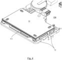
- the body of the memory card reader 11 is a part of generally rectangular parallelepiped shape, the base 11A and the cover 11B together forming an insertion slot 111 which allows a memory card to be inserted in a correct position so that it comes into contact with the memory card connector 10, once in the stop position.
- a memory card connector 10 is constructed independently of a body of the memory card reader 11.
- the memory card connector 10 is designed to enable reading of signals emanating from the memory card (not shown).
- the memory card connector 10 comprises a number of pins (eight on the [ Fig.5 ]), allowing contact with corresponding areas of the chip of the memory card (generally six or eight areas, depending on the type of memory card). These pins are generally metal spring blades which are positioned on the surface of the chip.
- the memory card connector 10 is furthermore intended to be connected to a main printed circuit, typically the motherboard CM of a memory card reading terminal in which it is installed, in order to ensure the operation of the memory card reader and its interconnection with the other components of the memory card reading terminal.
- a main printed circuit typically the motherboard CM of a memory card reading terminal in which it is installed
- this main printed circuit on which the connector 10 is for example soldered, is referred to as the “motherboard” CM.
- motherboard should not be understood in a restrictive sense, and that in certain embodiments the main printed circuit is not necessarily the motherboard of the reading terminal. Since the subject of the disclosure is not the memory card connector, its detailed description will not be made further.
- the memory card connector 10 is independent of the memory card reader body 11. In other words, the memory card connector 10 is not assembled with the memory card reader body 11 before being assembled to the motherboard CM of the memory card reading terminal: according to the proposed technique, the memory card connector 10 is first fixed on the motherboard CM, then the previously assembled memory card reader body 11 is placed over the connector 10 on the motherboard CM to be soldered there in the oven.
- the assembly and fixing of the memory card reader on the motherboard CM are simplified and can be carried out in a limited number of automated steps.
- the implementation of a memory card reader body 11 whose base and cover are made of metals makes it possible to reduce the manufacturing costs of such a memory card reader while offering a significant saving of space at the level of the motherboard CM.
- Such a saving of space at the level of the motherboard can make it possible to increase the dimensions of a keyboard for example.
- the memory card reader body 11 is, for example, a part of generally rectangular parallelepiped shape, with a width of approximately fifty-five millimeters, a depth of approximately thirty-two millimeters and a height of approximately four millimeters.
- the base 11A and the cover 11B together form an insertion slot 111 which allows a memory card to be inserted in a correct position so that it comes into contact with the memory card connector, once in the stop position.
- This insertion slot has a height of between 0.85 and 1.20 millimeters.
- the body of the memory card reader 11 comprises two main parts: a base 11A, a cover 11B.
- a printed circuit (not shown in the figures) surmounts the cover 11B in order to protect the body of the memory card reader from possible intrusions.
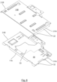
- the hood 11B has a generally rectangular parallelepiped shape, with a generally flat and rectangular main surface 20 and two side walls 21A, 21B of generally rectangular parallelepiped shape.
- the side walls 21A, 21B are substantially perpendicular to the main surface 20 of the cover 11B, and constitute means of assembly with a base 11A described later.
- the side walls 21A, 21B comprise fixing means 22, which can take the form of egg-shaped ends allowing the cover 11B to be fixed to the base 11A as will be described later.
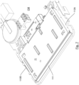
- the base 11A of the memory card reader body 11 is shown in more detail in connection with the [ Fig.6 ] in a particular embodiment of the proposed technique.
- the base 11A is also of generally rectangular parallelepiped shape.
- the side walls 31A, 31B are substantially perpendicular to the main surface 30 of the base 11A, and constitute means of assembly with the cover 11B.
- the side walls 31A, 31B comprise fixing means 32, which can take the form of egg-shaped ends allowing the cover 11B to be fixed to the base 11A as will be described later.
- the base 11A also comprises a housing 33 intended to receive the memory card connector 10 when mounting the body of the memory card reader 11 on the motherboard CM.
- This housing 33 takes the form of an orifice passing through the base 11A from one side to the other.
- the shape of this receiving housing 33 is substantially complementary to the shape of the memory card connector 10.
- the base 11A comprises centering pins (not shown), making it possible to ensure correct centering of the base 11A on the connector 10 during mounting.
- the base 11A being metallic, its shape can then for example be obtained very simply from a simple metal plate, by means of usual cutting and embossing techniques.
- the side walls 31A, 31B and the fixing means 32 can for example be obtained by simple folding and embossing of such a previously cut metal plate.
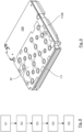
- the body of the memory card reader 11 is assembled automatically by a robot.
- the cover 11B is assembled with the base 11A.
- the fixing means 22 arranged on the side walls 21A, 21B of the cover 11B have just fixed in the fixing means 32 arranged on the side walls 31A, 31B of the base 11A.
- the side walls 21A, 21B, 31A and 31B thus assembled constitute the side walls 110A, 110B of the body of the memory card reader 11 which have a generally rectangular parallelepiped shape and extend substantially perpendicular to the lower face of said memory card reader body 11.
- step E2 the cover 11B and the base 11A, once assembled during step E1, are welded at the level of the fixing means 22 and 32.
- the card reader connector 10 is mounted on the CM motherboard.
- a material such as an abrasive paste, is applied to the lower surface of the side walls 110A, 110B of the body of the memory card reader 11.
- a step E4 the body of the memory card reader 11 is placed on the surface of the motherboard CM so that the connector 10 is housed in the housing 33 provided in the base 11A of the body of the memory card reader 11 and so that the lower surface of the side walls 110A, 110B covered with the material is in contact with the surface of the motherboard CM.
- step E5 everything is put in the oven so that the material placed between the bottom surface of the side walls 110A, 110B and the surface of the motherboard CM allows the welding of the memory card reader body 11 and the motherboard CM.
- Fig.9 represents a keyboard 40 arranged on a surface of the motherboard CM opposite the surface on which the body of the memory card reader is fixed. It can be seen in this figure that in the absence of the orifices 13 present on the motherboards of the prior art, it is possible to enlarge the keyboard 40.
- the characteristics presented in the different embodiments described are of course combinable individually or in groups with the general principle previously introduced, without departing from the scope of the present invention.
Landscapes
- Engineering & Computer Science (AREA)
- Physics & Mathematics (AREA)
- Health & Medical Sciences (AREA)
- Toxicology (AREA)
- Theoretical Computer Science (AREA)
- Artificial Intelligence (AREA)
- Computer Vision & Pattern Recognition (AREA)
- General Physics & Mathematics (AREA)
- Computer Security & Cryptography (AREA)
- Computer Networks & Wireless Communication (AREA)
- Electromagnetism (AREA)
- General Health & Medical Sciences (AREA)
- Manufacturing & Machinery (AREA)
- Mounting Of Printed Circuit Boards And The Like (AREA)
- Credit Cards Or The Like (AREA)
- Coupling Device And Connection With Printed Circuit (AREA)
Claims (6)
- Speicherkarten-Leserkörper (11), wobei der Leserkörper eine im Allgemeinen rechteckige Parallelepipedform hat und einen Einführschlitz (111) für eine Speicherkarte umfasst, wobei der Speicherkarten-Leserkörper eine Oberseite umfasst, die aus einer Abdeckung (11B) besteht, und eine Unterseite, die aus einer Basis (11A) besteht, in der eine Durchgangsöffnung (33) zur Aufnahme eines Speicherkartenverbinders (10) unabhängig vom Speicherkarten-Leserkörper ausgebildet ist, wobei der Speicherkarten-Leserkörper (10) in dem:- die Basis ein Metallstück ist, das erste Mittel (31A, 31B) zum Verbinden mit der Haube umfasst, die jeweils auf mindestens zwei gegenüberliegenden Seiten der Basis angeordnet sind,- die Haube ein Metallstück ist, das zweite Mittel (21A, 21B) zum Verbinden mit der Basis umfasst, die jeweils auf mindestens zwei gegenüberliegenden Seiten der Haube angeordnet sind, und- die ersten Verbindungsmittel dazu bestimmt sind, mit den zweiten Verbindungsmitteln ineinander zu greifen, um zwei Seitenwände (110A, 110B) des Speicherkartenleser-Körpers zu bilden, wobei die Seitenwände eine insgesamt rechteckige Parallelepipedform aufweisen und sich im Wesentlichen senkrecht zur Unterseite des Speicherkartenleser-Körpers erstrecken.
- Gehäuse eines Speicherkartenlesers nach Anspruch 1, bei dem nach dem Ineinanderstecken die ersten und zweiten Verbindungsmittel durch Schweißen aneinander befestigt sind.
- Gehäuse eines Speicherkartenlesers nach Anspruch 1, bei dem das Metall, aus dem die Abdeckung besteht, mit Kohlenstoffatomen dotiert ist.
- System zum Lesen von Speicherkarten, bestehend aus:- eine Hauptplatine (CM), auf deren einer Oberfläche ein Speicherkartensteckplatz befestigt ist, und- einen Speicherkartenleser-Körper nach Anspruch 1, der auf der genannten Oberfläche der Hauptplatine so angeordnet ist, dass der Speicherkartenverbinder innerhalb der Durchgangsöffnung (33) zur Aufnahme des genannten Speicherkartenverbinders des genannten Speicherkartenleser-Körpers Platz findet, das System, bei dem die Seitenwände (110A, 110B) des Speicherkartenleser-Körpers mit der Oberfläche der Hauptplatine mittels einer Materialzufuhr verschweißt sind, die zwischen einer unteren Oberfläche der Seitenwände des Speicherkartenleser-Körpers und der Oberfläche der Hauptplatine angeordnet ist.
- Verfahren zur Montage eines Speicherkarten-Lesesystems nach Anspruch 4, wobei das Verfahren umfasst:- einen Schritt des Befestigens des Speicherkartensteckers (10) an einer Oberfläche der Hauptplatine (CM),- einen Schritt des Aufsetzens des Speicherkartenleserkörpers auf die Oberfläche der Hauptplatine, so dass der Speicherkartenverbinder innerhalb der Durchgangsöffnung zur Aufnahme des Speicherkartenverbinders des Speicherkartenleserkörpers Platz findet,- einen Schritt des Befestigens der Seitenwände (110A, 110B) des Speicherkartenleserkörpers an der Oberfläche der Hauptplatine mittels einer Materialzufuhr, die zwischen einer unteren Oberfläche der Seitenwände des Speicherkartenleserkörpers und der Oberfläche der Hauptplatine angeordnet ist.
- Endgerät zum Lesen von Speicherkarten, das ein System zum Lesen von Speicherkarten nach Anspruch 4 umfasst.
Applications Claiming Priority (2)
| Application Number | Priority Date | Filing Date | Title |
|---|---|---|---|
| FR2011174A FR3115905B1 (fr) | 2020-10-30 | 2020-10-30 | Connecteur de carte à puce soudable et procédé de montage correspondant. |
| PCT/EP2021/080213 WO2022090516A1 (fr) | 2020-10-30 | 2021-10-29 | Connecteur de carte à puce soudable et procédé de montage correspondant |
Publications (2)
| Publication Number | Publication Date |
|---|---|
| EP4237988A1 EP4237988A1 (de) | 2023-09-06 |
| EP4237988B1 true EP4237988B1 (de) | 2025-01-22 |
Family
ID=73793514
Family Applications (1)
| Application Number | Title | Priority Date | Filing Date |
|---|---|---|---|
| EP21805434.4A Active EP4237988B1 (de) | 2020-10-30 | 2021-10-29 | Lötbarer chipkartenverbinder und entsprechendes montageverfahren |
Country Status (6)
| Country | Link |
|---|---|
| US (1) | US12136791B2 (de) |
| EP (1) | EP4237988B1 (de) |
| CA (1) | CA3196580A1 (de) |
| ES (1) | ES3018011T3 (de) |
| FR (1) | FR3115905B1 (de) |
| WO (1) | WO2022090516A1 (de) |
Family Cites Families (4)
| Publication number | Priority date | Publication date | Assignee | Title |
|---|---|---|---|---|
| FR2747847B1 (fr) | 1996-04-18 | 1998-07-03 | Itt Composants Instr | Boitier de raccordement electronique, a un ordinateur individuel, equipe d'un connecteur pour une carte a puce |
| DE69937103T2 (de) * | 1999-06-08 | 2008-06-12 | Molex Inc., Lisle | Tragbare Chipkarten-Leseanordnung |
| CN202205229U (zh) * | 2010-08-18 | 2012-04-25 | 刘建民 | 电子化标识装置、识读器和物品认证系统 |
| FR3085514B1 (fr) * | 2018-09-04 | 2021-09-10 | Ingenico Group | Terminal de lecture de carte a memoire comprenant un moyen de compensation d'inclinaison |
-
2020
- 2020-10-30 FR FR2011174A patent/FR3115905B1/fr active Active
-
2021
- 2021-10-29 EP EP21805434.4A patent/EP4237988B1/de active Active
- 2021-10-29 US US18/034,186 patent/US12136791B2/en active Active
- 2021-10-29 WO PCT/EP2021/080213 patent/WO2022090516A1/fr not_active Ceased
- 2021-10-29 ES ES21805434T patent/ES3018011T3/es active Active
- 2021-10-29 CA CA3196580A patent/CA3196580A1/fr active Pending
Also Published As
| Publication number | Publication date |
|---|---|
| ES3018011T3 (en) | 2025-05-14 |
| US20230411918A1 (en) | 2023-12-21 |
| FR3115905B1 (fr) | 2023-03-03 |
| US12136791B2 (en) | 2024-11-05 |
| CA3196580A1 (fr) | 2022-05-05 |
| EP4237988A1 (de) | 2023-09-06 |
| FR3115905A1 (fr) | 2022-05-06 |
| WO2022090516A1 (fr) | 2022-05-05 |
Similar Documents
| Publication | Publication Date | Title |
|---|---|---|
| EP3349139B1 (de) | Körper eines kartenlesegeräts mit gesichertem speicher | |
| FR2821988A1 (fr) | Connecteur electrique pour cartes a memoire electronique a grande capacite de stockage | |
| EP2915094B1 (de) | Kartenleserkörper mit gesicherten speicher | |
| EP3371735B1 (de) | Körper eines speicherkartenlesers mit einem schutznetz auf beiden seiten | |
| EP4237988B1 (de) | Lötbarer chipkartenverbinder und entsprechendes montageverfahren | |
| WO2007141418A1 (fr) | Dispositif de masquage pour objet portable sans contact de type document securise a dispositif radiofrequence | |
| EP2791859B1 (de) | Elektrostatische entladevorrichtung | |
| EP2915093B1 (de) | Sicherer verbinder für eine speicherkarte | |
| EP3063698B1 (de) | Verfahren zur herstellung eines speicherkartenleserkörpers, speicherkartenleserkörper und entsprechendes speicherkartenleser-terminal | |
| EP3063697B1 (de) | Speicherkartenleseanordnung inklusive intrusionsschutz | |
| EP3252652B1 (de) | Körper eines kartenlesegeräts mit gesichertem speicher | |
| EP3116070B1 (de) | Steckverbinder eines gesicherten integrierten schaltkreises | |
| FR3038780A1 (fr) | Connecteur de circuit integre securise | |
| FR3085514A1 (fr) | Terminal de lecture de carte a memoire comprenant un moyen de compensation d'inclinaison | |
| FR2997531A1 (fr) | Corps de lecteur de carte a memoire, pion d’ancrage et terminal de lecture de carte a memoire correspondants. | |
| EP3987431B1 (de) | Hybrides transaktionskartenlesesystem |
Legal Events
| Date | Code | Title | Description |
|---|---|---|---|
| STAA | Information on the status of an ep patent application or granted ep patent |
Free format text: STATUS: UNKNOWN |
|
| STAA | Information on the status of an ep patent application or granted ep patent |
Free format text: STATUS: THE INTERNATIONAL PUBLICATION HAS BEEN MADE |
|
| PUAI | Public reference made under article 153(3) epc to a published international application that has entered the european phase |
Free format text: ORIGINAL CODE: 0009012 |
|
| STAA | Information on the status of an ep patent application or granted ep patent |
Free format text: STATUS: REQUEST FOR EXAMINATION WAS MADE |
|
| 17P | Request for examination filed |
Effective date: 20230509 |
|
| AK | Designated contracting states |
Kind code of ref document: A1 Designated state(s): AL AT BE BG CH CY CZ DE DK EE ES FI FR GB GR HR HU IE IS IT LI LT LU LV MC MK MT NL NO PL PT RO RS SE SI SK SM TR |
|
| DAV | Request for validation of the european patent (deleted) | ||
| DAX | Request for extension of the european patent (deleted) | ||
| GRAP | Despatch of communication of intention to grant a patent |
Free format text: ORIGINAL CODE: EPIDOSNIGR1 |
|
| STAA | Information on the status of an ep patent application or granted ep patent |
Free format text: STATUS: GRANT OF PATENT IS INTENDED |
|
| INTG | Intention to grant announced |
Effective date: 20240903 |
|
| GRAS | Grant fee paid |
Free format text: ORIGINAL CODE: EPIDOSNIGR3 |
|
| GRAA | (expected) grant |
Free format text: ORIGINAL CODE: 0009210 |
|
| STAA | Information on the status of an ep patent application or granted ep patent |
Free format text: STATUS: THE PATENT HAS BEEN GRANTED |
|
| AK | Designated contracting states |
Kind code of ref document: B1 Designated state(s): AL AT BE BG CH CY CZ DE DK EE ES FI FR GB GR HR HU IE IS IT LI LT LU LV MC MK MT NL NO PL PT RO RS SE SI SK SM TR |
|
| REG | Reference to a national code |
Ref country code: GB Ref legal event code: FG4D Free format text: NOT ENGLISH |
|
| REG | Reference to a national code |
Ref country code: CH Ref legal event code: EP |
|
| REG | Reference to a national code |
Ref country code: IE Ref legal event code: FG4D Free format text: LANGUAGE OF EP DOCUMENT: FRENCH |
|
| REG | Reference to a national code |
Ref country code: DE Ref legal event code: R096 Ref document number: 602021025181 Country of ref document: DE |
|
| REG | Reference to a national code |
Ref country code: NL Ref legal event code: MP Effective date: 20250122 |
|
| PG25 | Lapsed in a contracting state [announced via postgrant information from national office to epo] |
Ref country code: NL Free format text: LAPSE BECAUSE OF FAILURE TO SUBMIT A TRANSLATION OF THE DESCRIPTION OR TO PAY THE FEE WITHIN THE PRESCRIBED TIME-LIMIT Effective date: 20250122 |
|
| PG25 | Lapsed in a contracting state [announced via postgrant information from national office to epo] |
Ref country code: RS Free format text: LAPSE BECAUSE OF FAILURE TO SUBMIT A TRANSLATION OF THE DESCRIPTION OR TO PAY THE FEE WITHIN THE PRESCRIBED TIME-LIMIT Effective date: 20250422 |
|
| PG25 | Lapsed in a contracting state [announced via postgrant information from national office to epo] |
Ref country code: FI Free format text: LAPSE BECAUSE OF FAILURE TO SUBMIT A TRANSLATION OF THE DESCRIPTION OR TO PAY THE FEE WITHIN THE PRESCRIBED TIME-LIMIT Effective date: 20250122 |
|
| PG25 | Lapsed in a contracting state [announced via postgrant information from national office to epo] |
Ref country code: PL Free format text: LAPSE BECAUSE OF FAILURE TO SUBMIT A TRANSLATION OF THE DESCRIPTION OR TO PAY THE FEE WITHIN THE PRESCRIBED TIME-LIMIT Effective date: 20250122 |
|
| REG | Reference to a national code |
Ref country code: LT Ref legal event code: MG9D |
|
| PG25 | Lapsed in a contracting state [announced via postgrant information from national office to epo] |
Ref country code: IS Free format text: LAPSE BECAUSE OF FAILURE TO SUBMIT A TRANSLATION OF THE DESCRIPTION OR TO PAY THE FEE WITHIN THE PRESCRIBED TIME-LIMIT Effective date: 20250522 Ref country code: NO Free format text: LAPSE BECAUSE OF FAILURE TO SUBMIT A TRANSLATION OF THE DESCRIPTION OR TO PAY THE FEE WITHIN THE PRESCRIBED TIME-LIMIT Effective date: 20250422 |
|
| REG | Reference to a national code |
Ref country code: AT Ref legal event code: MK05 Ref document number: 1761997 Country of ref document: AT Kind code of ref document: T Effective date: 20250122 |
|
| PG25 | Lapsed in a contracting state [announced via postgrant information from national office to epo] |
Ref country code: HR Free format text: LAPSE BECAUSE OF FAILURE TO SUBMIT A TRANSLATION OF THE DESCRIPTION OR TO PAY THE FEE WITHIN THE PRESCRIBED TIME-LIMIT Effective date: 20250122 |
|
| PG25 | Lapsed in a contracting state [announced via postgrant information from national office to epo] |
Ref country code: PT Free format text: LAPSE BECAUSE OF FAILURE TO SUBMIT A TRANSLATION OF THE DESCRIPTION OR TO PAY THE FEE WITHIN THE PRESCRIBED TIME-LIMIT Effective date: 20250522 Ref country code: LV Free format text: LAPSE BECAUSE OF FAILURE TO SUBMIT A TRANSLATION OF THE DESCRIPTION OR TO PAY THE FEE WITHIN THE PRESCRIBED TIME-LIMIT Effective date: 20250122 |
|
| PG25 | Lapsed in a contracting state [announced via postgrant information from national office to epo] |
Ref country code: GR Free format text: LAPSE BECAUSE OF FAILURE TO SUBMIT A TRANSLATION OF THE DESCRIPTION OR TO PAY THE FEE WITHIN THE PRESCRIBED TIME-LIMIT Effective date: 20250423 Ref country code: BG Free format text: LAPSE BECAUSE OF FAILURE TO SUBMIT A TRANSLATION OF THE DESCRIPTION OR TO PAY THE FEE WITHIN THE PRESCRIBED TIME-LIMIT Effective date: 20250122 |
|
| PG25 | Lapsed in a contracting state [announced via postgrant information from national office to epo] |
Ref country code: AT Free format text: LAPSE BECAUSE OF FAILURE TO SUBMIT A TRANSLATION OF THE DESCRIPTION OR TO PAY THE FEE WITHIN THE PRESCRIBED TIME-LIMIT Effective date: 20250122 |
|
| PG25 | Lapsed in a contracting state [announced via postgrant information from national office to epo] |
Ref country code: SE Free format text: LAPSE BECAUSE OF FAILURE TO SUBMIT A TRANSLATION OF THE DESCRIPTION OR TO PAY THE FEE WITHIN THE PRESCRIBED TIME-LIMIT Effective date: 20250122 |
|
| PG25 | Lapsed in a contracting state [announced via postgrant information from national office to epo] |
Ref country code: SM Free format text: LAPSE BECAUSE OF FAILURE TO SUBMIT A TRANSLATION OF THE DESCRIPTION OR TO PAY THE FEE WITHIN THE PRESCRIBED TIME-LIMIT Effective date: 20250122 |
|
| PG25 | Lapsed in a contracting state [announced via postgrant information from national office to epo] |
Ref country code: DK Free format text: LAPSE BECAUSE OF FAILURE TO SUBMIT A TRANSLATION OF THE DESCRIPTION OR TO PAY THE FEE WITHIN THE PRESCRIBED TIME-LIMIT Effective date: 20250122 |
|
| PG25 | Lapsed in a contracting state [announced via postgrant information from national office to epo] |
Ref country code: IT Free format text: LAPSE BECAUSE OF FAILURE TO SUBMIT A TRANSLATION OF THE DESCRIPTION OR TO PAY THE FEE WITHIN THE PRESCRIBED TIME-LIMIT Effective date: 20250122 |
|
| PG25 | Lapsed in a contracting state [announced via postgrant information from national office to epo] |
Ref country code: EE Free format text: LAPSE BECAUSE OF FAILURE TO SUBMIT A TRANSLATION OF THE DESCRIPTION OR TO PAY THE FEE WITHIN THE PRESCRIBED TIME-LIMIT Effective date: 20250122 Ref country code: CZ Free format text: LAPSE BECAUSE OF FAILURE TO SUBMIT A TRANSLATION OF THE DESCRIPTION OR TO PAY THE FEE WITHIN THE PRESCRIBED TIME-LIMIT Effective date: 20250122 |
|
| REG | Reference to a national code |
Ref country code: DE Ref legal event code: R097 Ref document number: 602021025181 Country of ref document: DE |
|
| PG25 | Lapsed in a contracting state [announced via postgrant information from national office to epo] |
Ref country code: RO Free format text: LAPSE BECAUSE OF FAILURE TO SUBMIT A TRANSLATION OF THE DESCRIPTION OR TO PAY THE FEE WITHIN THE PRESCRIBED TIME-LIMIT Effective date: 20250122 |
|
| PG25 | Lapsed in a contracting state [announced via postgrant information from national office to epo] |
Ref country code: SK Free format text: LAPSE BECAUSE OF FAILURE TO SUBMIT A TRANSLATION OF THE DESCRIPTION OR TO PAY THE FEE WITHIN THE PRESCRIBED TIME-LIMIT Effective date: 20250122 |
|
| PLBE | No opposition filed within time limit |
Free format text: ORIGINAL CODE: 0009261 |
|
| STAA | Information on the status of an ep patent application or granted ep patent |
Free format text: STATUS: NO OPPOSITION FILED WITHIN TIME LIMIT |
|
| 26N | No opposition filed |
Effective date: 20251023 |
|
| PGFP | Annual fee paid to national office [announced via postgrant information from national office to epo] |
Ref country code: DE Payment date: 20251021 Year of fee payment: 5 |
|
| PGFP | Annual fee paid to national office [announced via postgrant information from national office to epo] |
Ref country code: GB Payment date: 20251022 Year of fee payment: 5 |
|
| PGFP | Annual fee paid to national office [announced via postgrant information from national office to epo] |
Ref country code: FR Payment date: 20251030 Year of fee payment: 5 |
|
| PGFP | Annual fee paid to national office [announced via postgrant information from national office to epo] |
Ref country code: ES Payment date: 20251217 Year of fee payment: 5 |
|
| P01 | Opt-out of the competence of the unified patent court (upc) registered |
Free format text: CASE NUMBER: UPC_APP_0000402_4237988/2026 Effective date: 20260106 |