EP3063697B1 - Speicherkartenleseanordnung inklusive intrusionsschutz - Google Patents
Speicherkartenleseanordnung inklusive intrusionsschutz Download PDFInfo
- Publication number
- EP3063697B1 EP3063697B1 EP14789264.0A EP14789264A EP3063697B1 EP 3063697 B1 EP3063697 B1 EP 3063697B1 EP 14789264 A EP14789264 A EP 14789264A EP 3063697 B1 EP3063697 B1 EP 3063697B1
- Authority
- EP
- European Patent Office
- Prior art keywords
- memory card
- support
- dimensional element
- protected
- height
- Prior art date
- Legal status (The legal status is an assumption and is not a legal conclusion. Google has not performed a legal analysis and makes no representation as to the accuracy of the status listed.)
- Active
Links
Images


Classifications
-
- G—PHYSICS
- G06—COMPUTING OR CALCULATING; COUNTING
- G06K—GRAPHICAL DATA READING; PRESENTATION OF DATA; RECORD CARRIERS; HANDLING RECORD CARRIERS
- G06K7/00—Methods or arrangements for sensing record carriers, e.g. for reading patterns
- G06K7/0013—Methods or arrangements for sensing record carriers, e.g. for reading patterns by galvanic contacts, e.g. card connectors for ISO-7816 compliant smart cards or memory cards, e.g. SD card readers
- G06K7/0086—Methods or arrangements for sensing record carriers, e.g. for reading patterns by galvanic contacts, e.g. card connectors for ISO-7816 compliant smart cards or memory cards, e.g. SD card readers the connector comprising a circuit for steering the operations of the card connector
- G06K7/0091—Methods or arrangements for sensing record carriers, e.g. for reading patterns by galvanic contacts, e.g. card connectors for ISO-7816 compliant smart cards or memory cards, e.g. SD card readers the connector comprising a circuit for steering the operations of the card connector the circuit comprising an arrangement for avoiding intrusions and unwanted access to data inside of the connector
-
- H—ELECTRICITY
- H05—ELECTRIC TECHNIQUES NOT OTHERWISE PROVIDED FOR
- H05K—PRINTED CIRCUITS; CASINGS OR CONSTRUCTIONAL DETAILS OF ELECTRIC APPARATUS; MANUFACTURE OF ASSEMBLAGES OF ELECTRICAL COMPONENTS
- H05K1/00—Printed circuits
- H05K1/02—Details
- H05K1/0284—Details of three-dimensional rigid printed circuit boards
-
- B—PERFORMING OPERATIONS; TRANSPORTING
- B23—MACHINE TOOLS; METAL-WORKING NOT OTHERWISE PROVIDED FOR
- B23K—SOLDERING OR UNSOLDERING; WELDING; CLADDING OR PLATING BY SOLDERING OR WELDING; CUTTING BY APPLYING HEAT LOCALLY, e.g. FLAME CUTTING; WORKING BY LASER BEAM
- B23K1/00—Soldering, e.g. brazing, or unsoldering
- B23K1/0008—Soldering, e.g. brazing, or unsoldering specially adapted for particular articles or work
- B23K1/0016—Soldering of electronic components
-
- G—PHYSICS
- G06—COMPUTING OR CALCULATING; COUNTING
- G06F—ELECTRIC DIGITAL DATA PROCESSING
- G06F21/00—Security arrangements for protecting computers, components thereof, programs or data against unauthorised activity
- G06F21/70—Protecting specific internal or peripheral components, in which the protection of a component leads to protection of the entire computer
- G06F21/86—Secure or tamper-resistant housings
-
- H—ELECTRICITY
- H05—ELECTRIC TECHNIQUES NOT OTHERWISE PROVIDED FOR
- H05K—PRINTED CIRCUITS; CASINGS OR CONSTRUCTIONAL DETAILS OF ELECTRIC APPARATUS; MANUFACTURE OF ASSEMBLAGES OF ELECTRICAL COMPONENTS
- H05K1/00—Printed circuits
- H05K1/02—Details
- H05K1/0275—Security details, e.g. tampering prevention or detection
-
- H—ELECTRICITY
- H05—ELECTRIC TECHNIQUES NOT OTHERWISE PROVIDED FOR
- H05K—PRINTED CIRCUITS; CASINGS OR CONSTRUCTIONAL DETAILS OF ELECTRIC APPARATUS; MANUFACTURE OF ASSEMBLAGES OF ELECTRICAL COMPONENTS
- H05K3/00—Apparatus or processes for manufacturing printed circuits
- H05K3/10—Apparatus or processes for manufacturing printed circuits in which conductive material is applied to the insulating support in such a manner as to form the desired conductive pattern
-
- H—ELECTRICITY
- H05—ELECTRIC TECHNIQUES NOT OTHERWISE PROVIDED FOR
- H05K—PRINTED CIRCUITS; CASINGS OR CONSTRUCTIONAL DETAILS OF ELECTRIC APPARATUS; MANUFACTURE OF ASSEMBLAGES OF ELECTRICAL COMPONENTS
- H05K3/00—Apparatus or processes for manufacturing printed circuits
- H05K3/30—Assembling printed circuits with electric components, e.g. with resistors
- H05K3/32—Assembling printed circuits with electric components, e.g. with resistors electrically connecting electric components or wires to printed circuits
- H05K3/34—Assembling printed circuits with electric components, e.g. with resistors electrically connecting electric components or wires to printed circuits by soldering
-
- B—PERFORMING OPERATIONS; TRANSPORTING
- B23—MACHINE TOOLS; METAL-WORKING NOT OTHERWISE PROVIDED FOR
- B23K—SOLDERING OR UNSOLDERING; WELDING; CLADDING OR PLATING BY SOLDERING OR WELDING; CUTTING BY APPLYING HEAT LOCALLY, e.g. FLAME CUTTING; WORKING BY LASER BEAM
- B23K2101/00—Articles made by soldering, welding or cutting
- B23K2101/36—Electric or electronic devices
- B23K2101/42—Printed circuits
-
- H—ELECTRICITY
- H05—ELECTRIC TECHNIQUES NOT OTHERWISE PROVIDED FOR
- H05K—PRINTED CIRCUITS; CASINGS OR CONSTRUCTIONAL DETAILS OF ELECTRIC APPARATUS; MANUFACTURE OF ASSEMBLAGES OF ELECTRICAL COMPONENTS
- H05K2201/00—Indexing scheme relating to printed circuits covered by H05K1/00
- H05K2201/09—Shape and layout
- H05K2201/09209—Shape and layout details of conductors
- H05K2201/09372—Pads and lands
- H05K2201/09409—Multiple rows of pads, lands, terminals or dummy patterns; Multiple rows of mounted components
-
- H—ELECTRICITY
- H05—ELECTRIC TECHNIQUES NOT OTHERWISE PROVIDED FOR
- H05K—PRINTED CIRCUITS; CASINGS OR CONSTRUCTIONAL DETAILS OF ELECTRIC APPARATUS; MANUFACTURE OF ASSEMBLAGES OF ELECTRICAL COMPONENTS
- H05K2201/00—Indexing scheme relating to printed circuits covered by H05K1/00
- H05K2201/09—Shape and layout
- H05K2201/09209—Shape and layout details of conductors
- H05K2201/09654—Shape and layout details of conductors covering at least two types of conductors provided for in H05K2201/09218 - H05K2201/095
- H05K2201/09781—Dummy conductors, i.e. not used for normal transport of current; Dummy electrodes of components
-
- H—ELECTRICITY
- H05—ELECTRIC TECHNIQUES NOT OTHERWISE PROVIDED FOR
- H05K—PRINTED CIRCUITS; CASINGS OR CONSTRUCTIONAL DETAILS OF ELECTRIC APPARATUS; MANUFACTURE OF ASSEMBLAGES OF ELECTRICAL COMPONENTS
- H05K2201/00—Indexing scheme relating to printed circuits covered by H05K1/00
- H05K2201/09—Shape and layout
- H05K2201/09209—Shape and layout details of conductors
- H05K2201/09654—Shape and layout details of conductors covering at least two types of conductors provided for in H05K2201/09218 - H05K2201/095
- H05K2201/098—Special shape of the cross-section of conductors, e.g. very thick plated conductors
-
- H—ELECTRICITY
- H05—ELECTRIC TECHNIQUES NOT OTHERWISE PROVIDED FOR
- H05K—PRINTED CIRCUITS; CASINGS OR CONSTRUCTIONAL DETAILS OF ELECTRIC APPARATUS; MANUFACTURE OF ASSEMBLAGES OF ELECTRICAL COMPONENTS
- H05K2201/00—Indexing scheme relating to printed circuits covered by H05K1/00
- H05K2201/10—Details of components or other objects attached to or integrated in a printed circuit board
- H05K2201/10007—Types of components
- H05K2201/10204—Dummy component, dummy PCB or template, e.g. for monitoring, controlling of processes, comparing, scanning
-
- H—ELECTRICITY
- H05—ELECTRIC TECHNIQUES NOT OTHERWISE PROVIDED FOR
- H05K—PRINTED CIRCUITS; CASINGS OR CONSTRUCTIONAL DETAILS OF ELECTRIC APPARATUS; MANUFACTURE OF ASSEMBLAGES OF ELECTRICAL COMPONENTS
- H05K2203/00—Indexing scheme relating to apparatus or processes for manufacturing printed circuits covered by H05K3/00
- H05K2203/05—Patterning and lithography; Masks; Details of resist
- H05K2203/0548—Masks
- H05K2203/0551—Exposure mask directly printed on the PCB
-
- H—ELECTRICITY
- H05—ELECTRIC TECHNIQUES NOT OTHERWISE PROVIDED FOR
- H05K—PRINTED CIRCUITS; CASINGS OR CONSTRUCTIONAL DETAILS OF ELECTRIC APPARATUS; MANUFACTURE OF ASSEMBLAGES OF ELECTRICAL COMPONENTS
- H05K3/00—Apparatus or processes for manufacturing printed circuits
- H05K3/10—Apparatus or processes for manufacturing printed circuits in which conductive material is applied to the insulating support in such a manner as to form the desired conductive pattern
- H05K3/12—Apparatus or processes for manufacturing printed circuits in which conductive material is applied to the insulating support in such a manner as to form the desired conductive pattern using thick film techniques, e.g. printing techniques to apply the conductive material or similar techniques for applying conductive paste or ink patterns
- H05K3/1241—Apparatus or processes for manufacturing printed circuits in which conductive material is applied to the insulating support in such a manner as to form the desired conductive pattern using thick film techniques, e.g. printing techniques to apply the conductive material or similar techniques for applying conductive paste or ink patterns by ink-jet printing or drawing by dispensing
-
- H—ELECTRICITY
- H05—ELECTRIC TECHNIQUES NOT OTHERWISE PROVIDED FOR
- H05K—PRINTED CIRCUITS; CASINGS OR CONSTRUCTIONAL DETAILS OF ELECTRIC APPARATUS; MANUFACTURE OF ASSEMBLAGES OF ELECTRICAL COMPONENTS
- H05K3/00—Apparatus or processes for manufacturing printed circuits
- H05K3/10—Apparatus or processes for manufacturing printed circuits in which conductive material is applied to the insulating support in such a manner as to form the desired conductive pattern
- H05K3/12—Apparatus or processes for manufacturing printed circuits in which conductive material is applied to the insulating support in such a manner as to form the desired conductive pattern using thick film techniques, e.g. printing techniques to apply the conductive material or similar techniques for applying conductive paste or ink patterns
- H05K3/1275—Apparatus or processes for manufacturing printed circuits in which conductive material is applied to the insulating support in such a manner as to form the desired conductive pattern using thick film techniques, e.g. printing techniques to apply the conductive material or similar techniques for applying conductive paste or ink patterns by other printing techniques, e.g. letterpress printing, intaglio printing, lithographic printing, offset printing
-
- H—ELECTRICITY
- H05—ELECTRIC TECHNIQUES NOT OTHERWISE PROVIDED FOR
- H05K—PRINTED CIRCUITS; CASINGS OR CONSTRUCTIONAL DETAILS OF ELECTRIC APPARATUS; MANUFACTURE OF ASSEMBLAGES OF ELECTRICAL COMPONENTS
- H05K3/00—Apparatus or processes for manufacturing printed circuits
- H05K3/10—Apparatus or processes for manufacturing printed circuits in which conductive material is applied to the insulating support in such a manner as to form the desired conductive pattern
- H05K3/14—Apparatus or processes for manufacturing printed circuits in which conductive material is applied to the insulating support in such a manner as to form the desired conductive pattern using spraying techniques to apply the conductive material, e.g. vapour evaporation
- H05K3/143—Masks therefor
-
- H—ELECTRICITY
- H05—ELECTRIC TECHNIQUES NOT OTHERWISE PROVIDED FOR
- H05K—PRINTED CIRCUITS; CASINGS OR CONSTRUCTIONAL DETAILS OF ELECTRIC APPARATUS; MANUFACTURE OF ASSEMBLAGES OF ELECTRICAL COMPONENTS
- H05K3/00—Apparatus or processes for manufacturing printed circuits
- H05K3/22—Secondary treatment of printed circuits
- H05K3/24—Reinforcing of the conductive pattern
- H05K3/245—Reinforcing conductive patterns made by printing techniques or by other techniques for applying conductive pastes, inks or powders; Reinforcing other conductive patterns by such techniques
Definitions
- the invention lies in the field of electronics and more particularly the field relating to the protection of signals transiting in a circuit, in a magnetic reading head, or even to the protection of the balls of a matrix of balls (of the English “Bail Grid array” BGA) corresponding to an integrated circuit package intended to be soldered on a printed circuit.
- the invention therefore aims at an application in the field of terminals comprising memory card readers or readers with magnetic reading heads or comprising a BGA box.
- the subject of the invention is a memory card reading terminal comprising a memory card connector (CAM) intended to be inserted into the memory card reading terminal.
- a memory card reading terminal comprising a memory card connector (CAM) intended to be inserted into the memory card reading terminal.
- CAM memory card connector
- Such a terminal therefore comprises a memory card reader and can be a payment terminal or else an identification terminal.
- Memory card reading terminals with magnetic reading heads, or even comprising a BGA box, comprise, in addition to a memory card reader, a certain number of components such as a keyboard, a screen, one or more processors, memory, a power source.
- the terminals embed network communication functions, contactless memory card detection functions, coupon management functions (for example fidelity), etc.
- the terminals In addition to the multiplication of such auxiliary functions, the terminals must also be resistant to the various attacks or attempts at fraud to which they are frequently subjected. In order to obtain uniformity in the resistance of terminals to attacks, international standards have been enacted. In the area of payment, for example, the PCI PED ( Payment Card Industry - Pin Entry Device) standard lays down requirements for intrusion and detection of attempted attacks on terminals. This is not the only standard in force.
- PCI PED Payment Card Industry - Pin Entry Device
- the memory card reader in fact, remains a relatively weak link in the memory card reading terminal. This is due to the fact that the memory card reader comprises a memory card insertion slot, this slot making the inside of the terminal accessible from the outside.
- the smart card connector is the part of the smart card reader that comes into contact with the chip or microprocessor embedded in the smart card.
- the patent DE 10 2009 026466 B3 also describes a memory card reader connector with contacts and a plastic protective element which protects these contacts against any intrusion.
- EP 1 927 931 A1 also describes a memory card reader connector with contacts and a plastic protective element which protects these contacts against any intrusion.
- This memory card reader comprises a memory card reader body 10, comprising a memory card insertion slot 11.
- the memory card connector is directly integrated within the memory card reader. It comprises connection pins 12 to the printed circuit (PCB for " Printed Circuit Board " in English) 13 (partial view).
- the PCB 13 also includes electronic components 14. To protect the memory card reader 10, the latter is covered with a complete protection 15, as well as a frontal protection.
- FIG. 2A Another assembly is also illustrated by the figure 2A .
- the memory card connector 22 is independent of the body of the memory card reader 20.
- the memory card connector 22 is not assembled with the body of the card reader memory 20 before being assembled to the printed circuit (PCB) 230 of the reading terminal.
- the technique described proposes to fix the memory card connector 22 first on the PCB 230, then to fix the body of the memory card reader 20 above the memory card connector 22. In other words, it is understood that this assembly is not at all of the same nature as the assembly of the figure 1 since the memory card connector is covered by the body of the memory card reader which somehow protects it.
- the attacker seeks to access the I/O signal transiting on a metal blade 210 between the memory card (smart card) and the memory card connector.
- the metal blade 210 consists of a flexible part establishing contact with the memory card and a part soldered to the PCB 230.
- the attacker aims in particular to intercept the I/O signal via the part soldered to the PCB 230.
- the secret code entered by the customer when requesting the secret code which may be conveyed without encryption on certain smart cards.
- memory card readers have been provided with mesh protection.
- This protection makes it possible to avoid insertion by drilling the terminal.
- a short circuit is produced, thus causing the terminal to be put out of service.
- components are used to protect the "sensitive" signals passing through them. More specifically, in relation to the figure 2B representing an enlargement of the assembly configuration proposed in figure 2A , these components 23 are arranged on a support (generally a printed circuit board (PCB)) so as to form, by juxtaposition, baffles or physical protection barriers to make it difficult to access the sensitive signals which transit for example within the memory card connector 22.
- a support generally a printed circuit board (PCB)
- Such a physical barrier of components 23 could also be used in the classic assembly configuration represented by the figure 1 to protect electronic components 14.
- pins 21 (“pin” in English) of the memory card connector making it possible to come into contact with corresponding areas of the memory card.
- These pins 21 are generally the ends of metal spring blades 210 which are positioned on the surface of the memory card.
- the drawback of the current technique lies in the need to solder these components 23, close to the signal to be protected, which sometimes involves soldering defects, or unsoldering of damaging components (constituting the physical protection barrier, or even components in which the sensitive signals will pass) due to successive thermal stages. These welding or desoldering defects are difficult to detect and lead to integration difficulties, in particular when one of the components becomes unsoldered and consequently becomes mobile inside the electronic device and therefore a possible cause of its degradation. .
- such components 23 are conventionally referred to as “fictitious” components because their only function is physical protection of sensitive signals due to their arrangement on the support. These “fictitious” components are therefore not connected to other components and therefore have no electronic function.
- the technique described proposes a new solution which does not have the drawbacks of the prior art, in the form of an assembly according to claim 1 used in the manufacture of an electronic device, said assembly comprising at least one component to be protected and at least one three-dimensional element of height at least equal to the height of an electronic component, said three-dimensional element being arranged laterally facing said at least one component to be protected, According to the technique described, such a three-dimensional element is mainly made up of a brazing material.
- the technique described deviates from the conventional use of the brazing material conventionally making it possible to establish a junction between two elements, namely a component and a support generally corresponding to a printed circuit.
- the brazing material no longer has a junction function, but a function of physical protection of components.
- the component to be protected is a memory card connector and/or its connection pins, for which it is desired to avoid any disturbance of the signals passing through it.
- the physical protection against a malicious third party therefore takes the form of a three-dimensional element secured by one end to the support and mainly or even exclusively composed of a brazing material.
- Such a composition of the three-dimensional element makes it suitable for physically preventing, because of the three-dimensional volume that it forms, the access of an instrument, for example a thin metal blade inserted horizontally (in the case of a card with memory, under the memory card connector) aimed at connecting to the sensitive signals Indeed, thanks to this three-dimensional element, the blade is diverted from its insertion path and therefore does not manage to access the signal to be protected.
- an instrument for example a thin metal blade inserted horizontally (in the case of a card with memory, under the memory card connector) aimed at connecting to the sensitive signals.
- the three-dimensional element consisting mainly, or exclusively, of a brazing material according to the technique described, acts as a physical “wall” or “bulwark” of protection.
- such a three-dimensional element has the advantage of little disturbing the electronic operation of the electronic components present and active on the support, also called a printed circuit.
- Such three-dimensional protection elements also take advantage of the properties of the permanent soldering material which constitutes them.
- the brazing material has good three-dimensional resistance to climatic conditions, in particular humidity, and very good mechanical strength.
- a "brazing material” is also called “soldering paste”, “soldering cream”, “solder”...
- brazing material lies in the fact that the temperature necessary for it to assemble with the support and form the three-dimensional element is lower than the melting temperature of the support but also that of the connector of memory card to be protected. Indeed, by definition, the brazing is carried out without fusion of the edges of the elements to be assembled when this technique is used to join together two distinct elements.
- the formation of the three-dimensional protection element does not cause any thermal degradation of the memory card connector to be protected or even of the support.
- a welding material requires the fusion of the edges of the assembled elements which can generate degradation of the mechanical properties and the oxidation of the constituent elements of the support and of the support itself.
- brazing materials available on the market is almost infinite, which allows great flexibility in the design of the support according to the technique described. For example, it is possible to use two separate brazing materials associated with separate steps for joining components to the support, these two joining steps requiring separate joining temperatures.
- Such lead-free brazing materials are, for example, alloys based on tin, silver and copper. Alloys based on tin, silver and copper SnAgCu have no eutectic composition and, depending on their composition, have a melting temperature range between 217°C and 227°C (SnAg3Cu0.5: 217-218° C, SnAg3.9Cu0.6: 217-220°C, SnAg4Cu0.5: 217-220°C, SnAg1Cu0.5: 217-227°C).
- a section of the three-dimensional element according to the height of said support, has the shape of a flat disc whose flat rests on said support.
- the three-dimensional element in the form of a flat cylinder whose flat rests on said support.
- the height of said three-dimensional element is at least equal to 0.2 mm.
- Such a minimum height of the three-dimensional element allows physical protection in the event of insertion of a blade or an instrument aimed at degrading the component to be protected or even the input-output (I/O) connection of this component. .
- This height is greater than the standard height of 150 ⁇ m obtained with the classic junction function between two elements of a brazing material
- the use of the brazing material according to the technique described aims to increase the height of deposition with regard to the conventional use of junction, so as to form a three-dimensional protection element acting as a barrier.
- the height of the three-dimensional element is between 0.2 mm and 0.3 mm so as to protect components of small dimensions while limiting the size, in particular when it is sought, for example, to integrate such a support into ultra-flat memory card (CAM) connectors.
- CAM ultra-flat memory card
- said three-dimensional element forms a broken line so as to protect at least two sides of said component to be protected.
- This variant embodiment has the advantage of requiring only a single three-dimensional protection element to protect several sides of a component to be protected or else a group of components to be protected. Protection by a single three-dimensional protection element makes it possible to avoid multiple attachments of disjointed three-dimensional elements. The manufacture of the support according to the technique described is therefore simplified.
- the technique described also relates to an electronic device comprising a support according to the technique described as described above.
- such a device corresponds to a memory card connector, an electronic device comprising a microprocessor,
- the technique described relates to a terminal comprising an electronic device as described above.
- Such a terminal is a memory card reading terminal, in particular a track card, or any terminal requiring the protection of signals transiting in a circuit, in a magnetic reading head, or even the protection of the balls of a matrix of balls (from the English “Bail Grid array” BGA) corresponding to an integrated circuit package intended to be soldered on a printed circuit.
- the technique described also relates to a method of manufacturing a memory card assembly, said assembly comprising at least one memory card connector to be protected.
- the technique used for depositing the brazing material is for example of the “inkjet deposition” type, by etching, thin layers, etc.
- the volume of material deposited will be predetermined according to the deposition technique used so as to allow the subsequent formation of a three-dimensional element of height at least equal to the memory card connector to be protected.
- deposition mask is meant a screen allowing “printing by stencil” making it possible to reproduce several times the deposit of three-dimensional elements on a series of supports treated successively by the process according to the technique described.
- the opening or openings defined in the screen printing mask define the surfaces for depositing the brazing material which cover the area or areas of the support, also called surface(s) of the support corresponding to the joining surface , with the support, of the three-dimensional element or elements obtained after reflowing according to the technique described here.
- such a manufacturing method comprises a step of adjusting said height of said at least one three-dimensional element.
- such a height adjustment is for example obtained by varying the ratio between the width of the surface for depositing the permanent assembly material (corresponding to the width of the openings of the screen printing mask) and the width of the area of the support corresponding to the joining surface, with the support, of the three-dimensional element or elements obtained after the reflow.
- the thickness before reflow may be greater (an additional thickness due to a "bead" of solder paste is obtained for a length of the three-dimensional element perpendicular to the direction of passage), which can lead to a very significant overall thickness after reflow.
- the ratio R between the width L DEP of said deposit surface of said permanent assembly material and the width L o of said three-dimensional element is such that 2 ⁇ R ⁇ 4.
- This precaution makes it possible in particular to avoid reflow balls which could hinder the operation of the components of the support while having a sufficiently high three-dimensional element height.
- a ratio of four or five between the width L DEP of said deposition surface of said brazing material and the width L O of said three-dimensional element increases the risk of the appearance of conductive balls of assembly material.
- the ratio R between the width L DEP of said deposition surface of said brazing material and the width L O of said three-dimensional element is therefore such that 2 ⁇ R ⁇ 4.
- the width of said three-dimensional element obtained after passing through reflow is of the order of 1 mm and said width of deposit of said brazing material is of the order of 3 mm.
- the general principle of the technique described consists in modifying the constitution of a support comprising at least one component to be protected, by diverting the conventional use of a brazing material to form a three-dimensional element whose height is at least equal to the height of an electronic component to act as a physical protective barrier for the component to be protected.
- Such three-dimensional protection elements are therefore mainly formed from a brazing material that is inexpensive and easily available because it is also conventionally used to secure an electronic component to the support.
- this representation of the support according to the technique described corresponds to an “image” of the support between the step of deposition and the step of formation of the process for manufacturing the support as detailed below.
- this representation corresponds to the superimposition 30 of a mask (also called a stencil or screen printing screen), with the support.
- the components to be protected are represented by rectangles 31 on the superposition 30 of the mask and of the support corresponding to a printed circuit (PCB for "Printed Circuit Board " in English) also called an electronic card.
- PCB printed Circuit Board
- FIG. 3A eight rectangles corresponding to the solder pads of active components are shown. These eight rectangles 31 correspond, for example, to the eight connection pins 21 of the memory card connector 22 as represented according to the figure 2B . Among these eight pins, there is notably a pin on which the I/O signal to be protected is accessible.
- the superposition 30 of the mask and the support comprises, after deposition of the brazing material, layers also called deposition surfaces of this brazing material at the level of the openings 32 of the screen printing mask superimposed on the areas of the support 33 corresponding to the joining surface, with the support, of the three-dimensional elements obtained after the passage in remelting.
- layers of brazing material also called cream or brazing paste
- Such layers of brazing material have after deposition a greater width, and preferably about three times greater, than the width of the area of the support 33 covered by the three-dimensional element obtained after the passage in reflow according to the technique described here on which they are deposited, in order to avoid the generation of conductive balls during the passage in reflow, these conductive balls being able to degrade the operation of the components within the support.
- the support 38 After removing the screen printing mask and going through reflow and, the support 38 is obtained, finalized according to the technique described as shown in the Figure 3B .
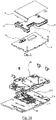
- the support 38 according to the technique described comprises three-dimensional elements 34, 35 and 36 for the physical protection of components to be protected which correspond according to the illustration of the Fig. 3C to the connection pins 21H of the independent memory card connector 39 of the memory card reading terminal 390 obtained after assembly of the memory card reader body 3900, with the support 38 obtained according to the technique described.
- connection between these two elements is made by means of an elastomer connector producing a permanent pressure, for example of the Zebra type (Registered trademark) (3901) as represented on the Fig. 3C .
- an elastomer connector producing a permanent pressure for example of the Zebra type (Registered trademark) (3901) as represented on the Fig. 3C .
- the memory card reader body also comprises openings allowing the insertion of metallic anchoring pins 3902, fixing, in the memory card reader body 3900, the support 38 obtained according to the technique described, these metal pins being soldered with solder paste (also called solder paste).
- solder paste also called solder paste
- Such metal anchoring pins hold the connector during repeated insertions of a memory card into the memory card reader.
- These metallic anchoring pins can also have a particular shape, adapted on the one hand to fulfill a function of guiding the memory card in the reader and on the other hand to carry out, if necessary, an electrostatic discharge of the edges of the card inserted.
- Each of these three-dimensional elements 34, 35, 36 are arranged laterally facing the component to be protected, namely the connection pins 21 H of the memory card connector, so as to "physically defend” them along at least one side such as a wall. or a rampart, against a possible malicious intrusion.
- composition of the three-dimensional element based on brazing material is that it allows great flexibility of shape and length of protective three-dimensional elements.
- three-dimensional elements in the form of a broken line such as element 36 which makes it possible to protect the components to be protected at an angle, but also elements of various lengths such as the long length of the three-dimensional element. 34 which makes it possible to replace four fictitious components of the prior art, or even the short length of the three-dimensional element 35 which makes it possible to obtain a protective barrier capable of being inserted into the housings of the metal spring blades 37 which are positioned on the surface of the chip.
- the three-dimensional elements 34 to 36 have the characteristic shape of a flat cylinder whose flat rests on the support. In other words, the section according to the height of the three-dimensional element in the form of a flat disc.
- this characteristic shape of the three-dimensional protection element according to the technique described is obtained during the passage through reflow.
- the capillarity of the corresponding brazing material according to the example illustrated in the figure 3A and 3B to a brazing material produces a grouping of the latter at the level of the pads of the support 33, and possibly a retraction of its volume.
- the three-dimensional element obtained after passing through reflow has a width substantially close to the width of the pads of the support 33.
- the shape resulting from this retraction by melting has characteristically a section according to the fault of the support, in the form of a flat disc and a height H at least equal to that of an electronic component of the order of 0, 2mm to 0.3mm to provide physical protection while allowing integration into an ultra-flat connector.
- a height H of 0.5 to 0.6 mm is obtained for a three-dimensional element whose length is perpendicular to the direction of passage of the scraper depositing brazing material
- a protective barrier corresponding to the three-dimensional element mainly consisting of a brazing material is easily identifiable with regard to the fictitious components used according to the prior art.
- the process amounts to manufacturing physical protection barriers for the memory card connector to be protected by depositing solder paste, using a screen printing process.
- solder paste using a screen printing process.
- English and also "over-printing" in English, corresponding to the fact that the deposit of solder paste is about three times wider than the width of the support covered by the three-dimensional element which will be obtained after the passage in reflow according to the technique described here.
- This mask comprises openings 32, as shown in relation to the Figure 3A . These openings 32 correspond to the deposit zones.
- Masks also called stencils or screen printing, are sometimes made from polyester sheets or copper alloys.
- the cutting of the openings 32 in the screen printing screen is for example carried out using laser beams, for example generated from laser diodes which allow fine cutting and rapid implementation.
- the profile of the opening 32 is often trapezoidal in shape, the base of which is in contact with the circuit, this to facilitate demolding.
- the solder paste 51 is pushed into the openings of the mask (not shown in the figure 5A ) by a squeegee to be deposited on the surface of the support 53.
- the support 53 is covered with a varnish 52, and has support areas, of width L o , "spared" from varnish, receiving the brazing material and corresponding to the joining surface, with the support, of the three-dimensional elements obtained after the passage in remelting once welded.
- the volume of solder paste to be deposited is for example determined by the surface of the reception area and the thickness of the stencil which is generally 150 ⁇ m. If the deposit is not sufficient, the protective three-dimensional element will not be secured correctly, if it is too large, the paste may overflow and cause bridges between areas.
- the quality of the deposit depends on many factors, the grain of the paste, its viscosity, the quality of the support, its thickness and the retention force on its walls, the dimensions of the opening, the temperature curves during the passage in the oven among others.
- the thickness of the stencil is also decisive.
- the adhesion of the paste to the walls depends on the ratio between the surface of the opening and the thickness of the material
- the adjustment REG 410 of this height consists, for example, in adjusting the ratio between the opening width 32 in the screen printing screen corresponding to the deposition width L DEP of the brazing material and the width L o of the area of the support covered by the three-dimensional element obtained after the passage in reflow.
- the deposition width L DEP of the brazing material is three times greater than the width L o the range of the support covered by the three-dimensional element obtained after the passage through reflow.
- Such a ratio ensures a sufficient height of the three-dimensional element, for example between 0.2 mm and 0.3 mm for a deposition width L DEP of the brazing material equal to 3 mm and a width L O the range of the support covered by the three-dimensional element obtained after the passage in remelting of 1mm, so that it plays the role of protection of sensitive components.
- COMP (411) is deposited, according to one option, the components to be protected.
- Depositing the components to be protected after the deposition of solder paste makes it possible to avoid any projection of solder paste on these components and therefore their potential degradation by this material.
- Such deposition of the components to be protected can optionally be carried out before or after removal of the deposition mask.
- the manufacturing process implements the formation (44) of the three-dimensional elements by reflowing them in a reflow oven, to obtain the suitable support. to be used to manufacture an electronic device such as a terminal (390) for reading a smart card, an example of which is shown in the Figure 3B .
- the advantage of using a brazing material to form the three-dimensional protection elements is that the temperature necessary for it to assemble with the support and form the three-dimensional element is lower than the melting temperature of the support but also that of the memory card connector. Degradation of the memory card connector is therefore avoided because during reflow only the solder paste reaches its melting temperature, that of the component not being reached.
- a three-dimensional element 55 is therefore obtained whose height H is for example between 0.2 mm and 0.3 mm for a deposition width L DEP of the brazing material equal to 3 mm and a width L O of the range of the support covered by the three-dimensional element obtained after passing through 1mm remelting.
- the width L o of the range of the support is therefore equal to the width of the surface of the three-dimensional element resting on the support (53). This height of the same order as that of an electronic component therefore acts as a protective wall.
- the three-dimensional protective elements of a support are also capable of protecting the components 14 of a conventional architecture such as that represented according to the figure 1 .
Landscapes
- Engineering & Computer Science (AREA)
- Theoretical Computer Science (AREA)
- Microelectronics & Electronic Packaging (AREA)
- Computer Security & Cryptography (AREA)
- Physics & Mathematics (AREA)
- General Physics & Mathematics (AREA)
- Computer Hardware Design (AREA)
- Manufacturing & Machinery (AREA)
- General Engineering & Computer Science (AREA)
- Software Systems (AREA)
- Artificial Intelligence (AREA)
- Computer Vision & Pattern Recognition (AREA)
- Mechanical Engineering (AREA)
- Electric Connection Of Electric Components To Printed Circuits (AREA)
- Credit Cards Or The Like (AREA)
- Coupling Device And Connection With Printed Circuit (AREA)
- Information Transfer Systems (AREA)
- Telephone Function (AREA)
Claims (7)
- Anordnung (390) zum Lesen von Speicherkarten, umfassend mindestens einen Speicherkartenlesekörper (3900) und einen Träger (38), wobei der Träger (38) mindestens einen zu schützenden (21) Speicherkartenanschluss (22) und mindestens ein dreidimensionales Element (34, 35, 36) von einer Höhe, die mindestens gleich der Höhe des zu schützenden (21) Speicherkartenanschlusses (22) ist, aufweist, wobei das dreidimensionale Element (34, 35, 36), das seitlich in Bezug auf den mindestens einen zu schützenden (21) Speicherkartenanschluss (22) angeordnet ist, einen physischen Schutz nach dem Zusammenfügen des Trägers (38) mit dem Speicherkartenlesekörper (3900) bildet, dadurch gekennzeichnet, dass das dreidimensionale Element (34, 35, 36) hauptsächlich aus einem Lötmaterial (51) besteht.
- Anordnung nach Anspruch 1, dadurch gekennzeichnet, dass ein Abschnitt des dreidimensionalen Elements (34, 35, 36) entlang der Höhe des Trägers die Form einer Scheibe (55) mit einer Abflachung (54) aufweist, deren Abflachung (54) auf dem Träger ruht.
- Anordnung nach einem der vorhergehenden Ansprüche, dadurch gekennzeichnet, dass die Höhe H des dreidimensionalen Elements mindestens 0,2 mm beträgt.
- Anordnung nach einem der vorhergehenden Ansprüche, dadurch gekennzeichnet, dass das dreidimensionale Element (36) eine unterbrochene Linie derart bildet, um mindestens zwei Seiten des mindestens eines Anschlusses (22) der zu schützenden Speicherkarte zu schützen.
- Verfahren zum Herstellen einer Anordnung (390) zum Lesen von Speicherkarten, umfassend mindestens einen Speicherkartenlesekörper (3900) und einen Träger (38), wobei der Träger mindestens einen zu schützenden Speicherkartenanschluss (22) aufweist, dadurch gekennzeichnet, dass das Verfahren zum Herstellen des Endgerätes (390) die folgenden Schritte aufweist:- Aufbringen (42) eines Lötmaterials (51) auf einer Aufbringfläche des Trägers (38),- Bilden (443) von mindestens einem dreidimensionalen Element von einer Höhe, die mindestens gleich der Höhe des zu schützenden (21) Speicherkartenanschlusses (22) ist, durch Umschmelzen des aufgebrachten Lötmaterials,- Bilden der Anordnung (390) zum Lesen von Speicherkarten mit dem Speicherkartenlesekörper (3900) und dem Träger (38), umfassend den zu schützenden (21) Speicherkartenanschluss (22).
- Verfahren zum Herstellen nach Anspruch 5, dadurch gekennzeichnet, dass es einen Schritt des Einstellens (410) der Höhe des mindestens einen dreidimensionalen Elements aufweist.
- Verfahren zum Herstellen nach Anspruch 5 oder 6, dadurch gekennzeichnet, das Verhältnis R zwischen der Breite LDEP der Aufbringfläche des Lötmaterials und der Breite Lo des dreidimensionalen Elements derart ist, dass 2<R<4 ist.
Applications Claiming Priority (2)
| Application Number | Priority Date | Filing Date | Title |
|---|---|---|---|
| FR1360602A FR3012719B1 (fr) | 2013-10-30 | 2013-10-30 | Support entrant dans la fabrication d'un dispositif electronique, connecteur de carte a memoire, terminal de lecture de carte a memoire et procede de fabrication correspondants |
| PCT/EP2014/072821 WO2015062981A1 (fr) | 2013-10-30 | 2014-10-24 | Support entrant dans la fabrication d'un dispositif électronique, connecteur de carte à mémoire, terminal de lecture de carte à mémoire et procédé de fabrication correspondants |
Publications (2)
| Publication Number | Publication Date |
|---|---|
| EP3063697A1 EP3063697A1 (de) | 2016-09-07 |
| EP3063697B1 true EP3063697B1 (de) | 2022-04-06 |
Family
ID=50489160
Family Applications (1)
| Application Number | Title | Priority Date | Filing Date |
|---|---|---|---|
| EP14789264.0A Active EP3063697B1 (de) | 2013-10-30 | 2014-10-24 | Speicherkartenleseanordnung inklusive intrusionsschutz |
Country Status (6)
| Country | Link |
|---|---|
| US (1) | US9980374B2 (de) |
| EP (1) | EP3063697B1 (de) |
| CA (1) | CA2927958C (de) |
| ES (1) | ES2918848T3 (de) |
| FR (1) | FR3012719B1 (de) |
| WO (1) | WO2015062981A1 (de) |
Families Citing this family (2)
| Publication number | Priority date | Publication date | Assignee | Title |
|---|---|---|---|---|
| US11201423B2 (en) * | 2020-07-15 | 2021-12-14 | Google Llc | Card connector assemblies with integrated component shielding |
| US12217107B2 (en) | 2023-01-25 | 2025-02-04 | Google Llc | Integrated memory card ejector and sensor ports |
Citations (1)
| Publication number | Priority date | Publication date | Assignee | Title |
|---|---|---|---|---|
| JP2007281274A (ja) * | 2006-04-10 | 2007-10-25 | Denso Corp | 半導体装置 |
Family Cites Families (8)
| Publication number | Priority date | Publication date | Assignee | Title |
|---|---|---|---|---|
| FR2805401A1 (fr) * | 2000-02-18 | 2001-08-24 | Itt Mfg Enterprises Inc | Connecteur electrique ergonomique pour carte a circuit(s) integre(s) |
| US7113410B2 (en) * | 2004-04-01 | 2006-09-26 | Lucent Technologies, Inc. | Electromagnetic shield assembly with opposed hook flanges |
| TWM261851U (en) * | 2004-08-17 | 2005-04-11 | Molex Taiwan Ltd | Electrical connector |
| FR2875036B1 (fr) * | 2004-09-07 | 2006-10-20 | Itt Mfg Enterprises Inc | Connecteur electrique pour carte a puce comportant des moyens de protection contre la fraude |
| US7633168B2 (en) * | 2006-06-28 | 2009-12-15 | Intel Corporation | Method, system, and apparatus for a secure bus on a printed circuit board |
| FR2909469B1 (fr) * | 2006-12-01 | 2009-01-02 | Itt Mfg Enterprises Inc | Agencement de securite contre la fraude pour connecteur electrique pour carte a puce |
| FR2944625B1 (fr) * | 2009-04-15 | 2012-03-09 | Ingenico Sa | Lecteur de carte memoire. |
| DE102009026466B3 (de) * | 2009-05-26 | 2010-07-01 | Ddm Hopt + Schuler Gmbh & Co. Kg | Manipulationsgeschützter Kartenleser |
-
2013
- 2013-10-30 FR FR1360602A patent/FR3012719B1/fr active Active
-
2014
- 2014-10-24 ES ES14789264T patent/ES2918848T3/es active Active
- 2014-10-24 EP EP14789264.0A patent/EP3063697B1/de active Active
- 2014-10-24 WO PCT/EP2014/072821 patent/WO2015062981A1/fr not_active Ceased
- 2014-10-24 CA CA2927958A patent/CA2927958C/en active Active
- 2014-10-24 US US15/033,836 patent/US9980374B2/en active Active
Patent Citations (1)
| Publication number | Priority date | Publication date | Assignee | Title |
|---|---|---|---|---|
| JP2007281274A (ja) * | 2006-04-10 | 2007-10-25 | Denso Corp | 半導体装置 |
Non-Patent Citations (2)
| Title |
|---|
| RAFAL WRONA ET AL: "Resistance of BGA Contacts During Reliability Tests", ELECTRONICS TECHNOLOGY, 30TH INTERNATIONAL SPRING SEMINAR ON, IEEE, PI, 1 May 2007 (2007-05-01), pages 162 - 166, XP031203626, ISBN: 978-1-4244-1217-4 * |
| RAINER DUDEK ET AL: "Fatigue Life Prediction and Analysis of Wafer Level Packages with SnAgCu Solder Balls", 1ST ELECTRONICS SYSTEMINTEGRATION TECHNOLOGY CONFERENCE, IEEE, PI, 1 September 2006 (2006-09-01), pages 903 - 911, XP031008487, ISBN: 978-1-4244-0552-7 * |
Also Published As
| Publication number | Publication date |
|---|---|
| CA2927958C (en) | 2023-09-19 |
| FR3012719B1 (fr) | 2017-04-14 |
| WO2015062981A1 (fr) | 2015-05-07 |
| ES2918848T3 (es) | 2022-07-20 |
| CA2927958A1 (en) | 2015-05-07 |
| EP3063697A1 (de) | 2016-09-07 |
| FR3012719A1 (fr) | 2015-05-01 |
| US9980374B2 (en) | 2018-05-22 |
| US20160270219A1 (en) | 2016-09-15 |
Similar Documents
| Publication | Publication Date | Title |
|---|---|---|
| EP3349139B1 (de) | Körper eines kartenlesegeräts mit gesichertem speicher | |
| EP3437028B1 (de) | Verfahren zur herstellung von chipkarten und von chipkartenantennenträgern | |
| FR2731869A1 (fr) | Carte de circuit et procede de fabrication de cette carte de circuit | |
| EP3063697B1 (de) | Speicherkartenleseanordnung inklusive intrusionsschutz | |
| EP2143312B1 (de) | Vorrichtung zum schutz einer elektronischen komponente | |
| EP3992855A1 (de) | Verfahren zur herstellung eines chipkarten-moduls mit einer geschweissten elektronischen komponente | |
| WO2003026010A1 (fr) | Étiquette électronique de faible épaisseur et procédé de fabrication d'une telle étiquette | |
| EP3371735B1 (de) | Körper eines speicherkartenlesers mit einem schutznetz auf beiden seiten | |
| FR2985153A1 (fr) | Dispositif de protection d'un circuit imprime electronique. | |
| WO2014067905A1 (fr) | Corps de lecteur de carte à mémoire sécurisé | |
| EP3063698B1 (de) | Verfahren zur herstellung eines speicherkartenleserkörpers, speicherkartenleserkörper und entsprechendes speicherkartenleser-terminal | |
| EP4237988B1 (de) | Lötbarer chipkartenverbinder und entsprechendes montageverfahren | |
| EP2915093A1 (de) | Sicherer verbinder für eine speicherkarte | |
| EP2953433B1 (de) | Herstellungsverfahren einer konfigurierbaren elektrischen komponente | |
| EP3116070B1 (de) | Steckverbinder eines gesicherten integrierten schaltkreises | |
| EP3220726A1 (de) | Elektronische karte, die einen zwischenschaltkreis mit metallisierten halblöchern umfasst | |
| FR3038780A1 (fr) | Connecteur de circuit integre securise | |
| EP2862424B1 (de) | Verfahren zur herstellung einer elektronischen schaltung mit schutz der leitenden schicht | |
| EP4704542A1 (de) | 3d-schutzstruktur gegen elektromagnetische interferenzen für halbleitervorrichtung | |
| FR3038103A1 (fr) | Module a puce electronique anti-intrusion | |
| WO2004100623A2 (fr) | Systeme electronique a zones d’echappatoire d’eventuels surplus de matiere fusible, et procede d’assemblage correspondant | |
| FR2997531A1 (fr) | Corps de lecteur de carte a memoire, pion d’ancrage et terminal de lecture de carte a memoire correspondants. |
Legal Events
| Date | Code | Title | Description |
|---|---|---|---|
| PUAI | Public reference made under article 153(3) epc to a published international application that has entered the european phase |
Free format text: ORIGINAL CODE: 0009012 |
|
| 17P | Request for examination filed |
Effective date: 20160429 |
|
| AK | Designated contracting states |
Kind code of ref document: A1 Designated state(s): AL AT BE BG CH CY CZ DE DK EE ES FI FR GB GR HR HU IE IS IT LI LT LU LV MC MK MT NL NO PL PT RO RS SE SI SK SM TR |
|
| AX | Request for extension of the european patent |
Extension state: BA ME |
|
| DAX | Request for extension of the european patent (deleted) | ||
| STAA | Information on the status of an ep patent application or granted ep patent |
Free format text: STATUS: EXAMINATION IS IN PROGRESS |
|
| 17Q | First examination report despatched |
Effective date: 20190905 |
|
| GRAP | Despatch of communication of intention to grant a patent |
Free format text: ORIGINAL CODE: EPIDOSNIGR1 |
|
| STAA | Information on the status of an ep patent application or granted ep patent |
Free format text: STATUS: GRANT OF PATENT IS INTENDED |
|
| RIC1 | Information provided on ipc code assigned before grant |
Ipc: H05K 3/24 20060101ALN20210212BHEP Ipc: G06F 21/86 20130101ALN20210212BHEP Ipc: H05K 3/12 20060101ALI20210212BHEP Ipc: B23K 101/42 20060101ALN20210212BHEP Ipc: H05K 1/02 20060101ALI20210212BHEP Ipc: H05K 3/14 20060101ALN20210212BHEP Ipc: G06K 7/00 20060101AFI20210212BHEP |
|
| RIC1 | Information provided on ipc code assigned before grant |
Ipc: H05K 3/12 20060101ALN20210225BHEP Ipc: H05K 3/14 20060101ALN20210225BHEP Ipc: G06K 7/00 20060101AFI20210225BHEP Ipc: G06F 21/86 20130101ALI20210225BHEP Ipc: B23K 101/42 20060101ALN20210225BHEP Ipc: H05K 1/02 20060101ALI20210225BHEP Ipc: H05K 3/24 20060101ALN20210225BHEP |
|
| INTG | Intention to grant announced |
Effective date: 20210311 |
|
| RAP3 | Party data changed (applicant data changed or rights of an application transferred) |
Owner name: INGENICO GROUP |
|
| GRAJ | Information related to disapproval of communication of intention to grant by the applicant or resumption of examination proceedings by the epo deleted |
Free format text: ORIGINAL CODE: EPIDOSDIGR1 |
|
| STAA | Information on the status of an ep patent application or granted ep patent |
Free format text: STATUS: EXAMINATION IS IN PROGRESS |
|
| GRAS | Grant fee paid |
Free format text: ORIGINAL CODE: EPIDOSNIGR3 |
|
| STAA | Information on the status of an ep patent application or granted ep patent |
Free format text: STATUS: GRANT OF PATENT IS INTENDED |
|
| GRAP | Despatch of communication of intention to grant a patent |
Free format text: ORIGINAL CODE: EPIDOSNIGR1 |
|
| INTC | Intention to grant announced (deleted) | ||
| INTG | Intention to grant announced |
Effective date: 20210709 |
|
| RIC1 | Information provided on ipc code assigned before grant |
Ipc: G06K 7/00 20060101AFI20210625BHEP Ipc: H05K 1/02 20060101ALI20210625BHEP Ipc: G06F 21/86 20130101ALI20210625BHEP Ipc: H05K 3/14 20060101ALN20210625BHEP Ipc: H05K 3/24 20060101ALN20210625BHEP Ipc: B23K 101/42 20060101ALN20210625BHEP Ipc: H05K 3/12 20060101ALN20210625BHEP |
|
| GRAA | (expected) grant |
Free format text: ORIGINAL CODE: 0009210 |
|
| STAA | Information on the status of an ep patent application or granted ep patent |
Free format text: STATUS: THE PATENT HAS BEEN GRANTED |
|
| RAP1 | Party data changed (applicant data changed or rights of an application transferred) |
Owner name: BANKS AND ACQUIRERS INTERNATIONAL HOLDING |
|
| AK | Designated contracting states |
Kind code of ref document: B1 Designated state(s): AL AT BE BG CH CY CZ DE DK EE ES FI FR GB GR HR HU IE IS IT LI LT LU LV MC MK MT NL NO PL PT RO RS SE SI SK SM TR |
|
| REG | Reference to a national code |
Ref country code: GB Ref legal event code: FG4D Free format text: NOT ENGLISH |
|
| REG | Reference to a national code |
Ref country code: CH Ref legal event code: EP |
|
| REG | Reference to a national code |
Ref country code: AT Ref legal event code: REF Ref document number: 1482087 Country of ref document: AT Kind code of ref document: T Effective date: 20220415 |
|
| REG | Reference to a national code |
Ref country code: IE Ref legal event code: FG4D Free format text: LANGUAGE OF EP DOCUMENT: FRENCH |
|
| REG | Reference to a national code |
Ref country code: DE Ref legal event code: R096 Ref document number: 602014083125 Country of ref document: DE |
|
| REG | Reference to a national code |
Ref country code: ES Ref legal event code: FG2A Ref document number: 2918848 Country of ref document: ES Kind code of ref document: T3 Effective date: 20220720 |
|
| REG | Reference to a national code |
Ref country code: LT Ref legal event code: MG9D |
|
| REG | Reference to a national code |
Ref country code: NL Ref legal event code: MP Effective date: 20220406 |
|
| REG | Reference to a national code |
Ref country code: AT Ref legal event code: MK05 Ref document number: 1482087 Country of ref document: AT Kind code of ref document: T Effective date: 20220406 |
|
| PG25 | Lapsed in a contracting state [announced via postgrant information from national office to epo] |
Ref country code: NL Free format text: LAPSE BECAUSE OF FAILURE TO SUBMIT A TRANSLATION OF THE DESCRIPTION OR TO PAY THE FEE WITHIN THE PRESCRIBED TIME-LIMIT Effective date: 20220406 |
|
| PG25 | Lapsed in a contracting state [announced via postgrant information from national office to epo] |
Ref country code: SE Free format text: LAPSE BECAUSE OF FAILURE TO SUBMIT A TRANSLATION OF THE DESCRIPTION OR TO PAY THE FEE WITHIN THE PRESCRIBED TIME-LIMIT Effective date: 20220406 Ref country code: PT Free format text: LAPSE BECAUSE OF FAILURE TO SUBMIT A TRANSLATION OF THE DESCRIPTION OR TO PAY THE FEE WITHIN THE PRESCRIBED TIME-LIMIT Effective date: 20220808 Ref country code: NO Free format text: LAPSE BECAUSE OF FAILURE TO SUBMIT A TRANSLATION OF THE DESCRIPTION OR TO PAY THE FEE WITHIN THE PRESCRIBED TIME-LIMIT Effective date: 20220706 Ref country code: LT Free format text: LAPSE BECAUSE OF FAILURE TO SUBMIT A TRANSLATION OF THE DESCRIPTION OR TO PAY THE FEE WITHIN THE PRESCRIBED TIME-LIMIT Effective date: 20220406 Ref country code: HR Free format text: LAPSE BECAUSE OF FAILURE TO SUBMIT A TRANSLATION OF THE DESCRIPTION OR TO PAY THE FEE WITHIN THE PRESCRIBED TIME-LIMIT Effective date: 20220406 Ref country code: GR Free format text: LAPSE BECAUSE OF FAILURE TO SUBMIT A TRANSLATION OF THE DESCRIPTION OR TO PAY THE FEE WITHIN THE PRESCRIBED TIME-LIMIT Effective date: 20220707 Ref country code: FI Free format text: LAPSE BECAUSE OF FAILURE TO SUBMIT A TRANSLATION OF THE DESCRIPTION OR TO PAY THE FEE WITHIN THE PRESCRIBED TIME-LIMIT Effective date: 20220406 Ref country code: BG Free format text: LAPSE BECAUSE OF FAILURE TO SUBMIT A TRANSLATION OF THE DESCRIPTION OR TO PAY THE FEE WITHIN THE PRESCRIBED TIME-LIMIT Effective date: 20220706 Ref country code: AT Free format text: LAPSE BECAUSE OF FAILURE TO SUBMIT A TRANSLATION OF THE DESCRIPTION OR TO PAY THE FEE WITHIN THE PRESCRIBED TIME-LIMIT Effective date: 20220406 |
|
| PG25 | Lapsed in a contracting state [announced via postgrant information from national office to epo] |
Ref country code: RS Free format text: LAPSE BECAUSE OF FAILURE TO SUBMIT A TRANSLATION OF THE DESCRIPTION OR TO PAY THE FEE WITHIN THE PRESCRIBED TIME-LIMIT Effective date: 20220406 Ref country code: PL Free format text: LAPSE BECAUSE OF FAILURE TO SUBMIT A TRANSLATION OF THE DESCRIPTION OR TO PAY THE FEE WITHIN THE PRESCRIBED TIME-LIMIT Effective date: 20220406 Ref country code: LV Free format text: LAPSE BECAUSE OF FAILURE TO SUBMIT A TRANSLATION OF THE DESCRIPTION OR TO PAY THE FEE WITHIN THE PRESCRIBED TIME-LIMIT Effective date: 20220406 Ref country code: IS Free format text: LAPSE BECAUSE OF FAILURE TO SUBMIT A TRANSLATION OF THE DESCRIPTION OR TO PAY THE FEE WITHIN THE PRESCRIBED TIME-LIMIT Effective date: 20220806 |
|
| REG | Reference to a national code |
Ref country code: DE Ref legal event code: R097 Ref document number: 602014083125 Country of ref document: DE |
|
| PG25 | Lapsed in a contracting state [announced via postgrant information from national office to epo] |
Ref country code: SM Free format text: LAPSE BECAUSE OF FAILURE TO SUBMIT A TRANSLATION OF THE DESCRIPTION OR TO PAY THE FEE WITHIN THE PRESCRIBED TIME-LIMIT Effective date: 20220406 Ref country code: SK Free format text: LAPSE BECAUSE OF FAILURE TO SUBMIT A TRANSLATION OF THE DESCRIPTION OR TO PAY THE FEE WITHIN THE PRESCRIBED TIME-LIMIT Effective date: 20220406 Ref country code: RO Free format text: LAPSE BECAUSE OF FAILURE TO SUBMIT A TRANSLATION OF THE DESCRIPTION OR TO PAY THE FEE WITHIN THE PRESCRIBED TIME-LIMIT Effective date: 20220406 Ref country code: EE Free format text: LAPSE BECAUSE OF FAILURE TO SUBMIT A TRANSLATION OF THE DESCRIPTION OR TO PAY THE FEE WITHIN THE PRESCRIBED TIME-LIMIT Effective date: 20220406 Ref country code: DK Free format text: LAPSE BECAUSE OF FAILURE TO SUBMIT A TRANSLATION OF THE DESCRIPTION OR TO PAY THE FEE WITHIN THE PRESCRIBED TIME-LIMIT Effective date: 20220406 Ref country code: CZ Free format text: LAPSE BECAUSE OF FAILURE TO SUBMIT A TRANSLATION OF THE DESCRIPTION OR TO PAY THE FEE WITHIN THE PRESCRIBED TIME-LIMIT Effective date: 20220406 |
|
| PLBE | No opposition filed within time limit |
Free format text: ORIGINAL CODE: 0009261 |
|
| STAA | Information on the status of an ep patent application or granted ep patent |
Free format text: STATUS: NO OPPOSITION FILED WITHIN TIME LIMIT |
|
| 26N | No opposition filed |
Effective date: 20230110 |
|
| PG25 | Lapsed in a contracting state [announced via postgrant information from national office to epo] |
Ref country code: AL Free format text: LAPSE BECAUSE OF FAILURE TO SUBMIT A TRANSLATION OF THE DESCRIPTION OR TO PAY THE FEE WITHIN THE PRESCRIBED TIME-LIMIT Effective date: 20220406 |
|
| PG25 | Lapsed in a contracting state [announced via postgrant information from national office to epo] |
Ref country code: SI Free format text: LAPSE BECAUSE OF FAILURE TO SUBMIT A TRANSLATION OF THE DESCRIPTION OR TO PAY THE FEE WITHIN THE PRESCRIBED TIME-LIMIT Effective date: 20220406 Ref country code: MC Free format text: LAPSE BECAUSE OF FAILURE TO SUBMIT A TRANSLATION OF THE DESCRIPTION OR TO PAY THE FEE WITHIN THE PRESCRIBED TIME-LIMIT Effective date: 20220406 |
|
| REG | Reference to a national code |
Ref country code: CH Ref legal event code: PL |
|
| REG | Reference to a national code |
Ref country code: BE Ref legal event code: MM Effective date: 20221031 |
|
| PG25 | Lapsed in a contracting state [announced via postgrant information from national office to epo] |
Ref country code: LU Free format text: LAPSE BECAUSE OF NON-PAYMENT OF DUE FEES Effective date: 20221024 |
|
| PG25 | Lapsed in a contracting state [announced via postgrant information from national office to epo] |
Ref country code: LI Free format text: LAPSE BECAUSE OF NON-PAYMENT OF DUE FEES Effective date: 20221031 Ref country code: CH Free format text: LAPSE BECAUSE OF NON-PAYMENT OF DUE FEES Effective date: 20221031 |
|
| PG25 | Lapsed in a contracting state [announced via postgrant information from national office to epo] |
Ref country code: BE Free format text: LAPSE BECAUSE OF NON-PAYMENT OF DUE FEES Effective date: 20221031 |
|
| PG25 | Lapsed in a contracting state [announced via postgrant information from national office to epo] |
Ref country code: IE Free format text: LAPSE BECAUSE OF NON-PAYMENT OF DUE FEES Effective date: 20221024 |
|
| PG25 | Lapsed in a contracting state [announced via postgrant information from national office to epo] |
Ref country code: IT Free format text: LAPSE BECAUSE OF FAILURE TO SUBMIT A TRANSLATION OF THE DESCRIPTION OR TO PAY THE FEE WITHIN THE PRESCRIBED TIME-LIMIT Effective date: 20220406 |
|
| PG25 | Lapsed in a contracting state [announced via postgrant information from national office to epo] |
Ref country code: HU Free format text: LAPSE BECAUSE OF FAILURE TO SUBMIT A TRANSLATION OF THE DESCRIPTION OR TO PAY THE FEE WITHIN THE PRESCRIBED TIME-LIMIT; INVALID AB INITIO Effective date: 20141024 |
|
| PG25 | Lapsed in a contracting state [announced via postgrant information from national office to epo] |
Ref country code: CY Free format text: LAPSE BECAUSE OF FAILURE TO SUBMIT A TRANSLATION OF THE DESCRIPTION OR TO PAY THE FEE WITHIN THE PRESCRIBED TIME-LIMIT Effective date: 20220406 |
|
| PG25 | Lapsed in a contracting state [announced via postgrant information from national office to epo] |
Ref country code: MK Free format text: LAPSE BECAUSE OF FAILURE TO SUBMIT A TRANSLATION OF THE DESCRIPTION OR TO PAY THE FEE WITHIN THE PRESCRIBED TIME-LIMIT Effective date: 20220406 |
|
| PG25 | Lapsed in a contracting state [announced via postgrant information from national office to epo] |
Ref country code: MT Free format text: LAPSE BECAUSE OF FAILURE TO SUBMIT A TRANSLATION OF THE DESCRIPTION OR TO PAY THE FEE WITHIN THE PRESCRIBED TIME-LIMIT Effective date: 20220406 |
|
| PG25 | Lapsed in a contracting state [announced via postgrant information from national office to epo] |
Ref country code: BG Free format text: LAPSE BECAUSE OF FAILURE TO SUBMIT A TRANSLATION OF THE DESCRIPTION OR TO PAY THE FEE WITHIN THE PRESCRIBED TIME-LIMIT Effective date: 20220406 |
|
| PG25 | Lapsed in a contracting state [announced via postgrant information from national office to epo] |
Ref country code: BG Free format text: LAPSE BECAUSE OF FAILURE TO SUBMIT A TRANSLATION OF THE DESCRIPTION OR TO PAY THE FEE WITHIN THE PRESCRIBED TIME-LIMIT Effective date: 20220406 |
|
| PG25 | Lapsed in a contracting state [announced via postgrant information from national office to epo] |
Ref country code: TR Free format text: LAPSE BECAUSE OF FAILURE TO SUBMIT A TRANSLATION OF THE DESCRIPTION OR TO PAY THE FEE WITHIN THE PRESCRIBED TIME-LIMIT Effective date: 20220406 |
|
| PGFP | Annual fee paid to national office [announced via postgrant information from national office to epo] |
Ref country code: DE Payment date: 20251021 Year of fee payment: 12 |
|
| PGFP | Annual fee paid to national office [announced via postgrant information from national office to epo] |
Ref country code: GB Payment date: 20251022 Year of fee payment: 12 |
|
| PGFP | Annual fee paid to national office [announced via postgrant information from national office to epo] |
Ref country code: FR Payment date: 20251030 Year of fee payment: 12 |
|
| PGFP | Annual fee paid to national office [announced via postgrant information from national office to epo] |
Ref country code: ES Payment date: 20251210 Year of fee payment: 12 |
|
| P01 | Opt-out of the competence of the unified patent court (upc) registered |
Free format text: CASE NUMBER: UPC_APP_0000324_3063697/2026 Effective date: 20260106 |