EP3349251A1 - Cellule solaire à haut rendement et procédé de fabrication de cellule solaire à haut rendement - Google Patents
Cellule solaire à haut rendement et procédé de fabrication de cellule solaire à haut rendement Download PDFInfo
- Publication number
- EP3349251A1 EP3349251A1 EP16886815.6A EP16886815A EP3349251A1 EP 3349251 A1 EP3349251 A1 EP 3349251A1 EP 16886815 A EP16886815 A EP 16886815A EP 3349251 A1 EP3349251 A1 EP 3349251A1
- Authority
- EP
- European Patent Office
- Prior art keywords
- solar cell
- emitter
- base
- insulator film
- conductivity type
- Prior art date
- Legal status (The legal status is an assumption and is not a legal conclusion. Google has not performed a legal analysis and makes no representation as to the accuracy of the status listed.)
- Granted
Links
Images


Classifications
-
- H—ELECTRICITY
- H10—SEMICONDUCTOR DEVICES; ELECTRIC SOLID-STATE DEVICES NOT OTHERWISE PROVIDED FOR
- H10F—INORGANIC SEMICONDUCTOR DEVICES SENSITIVE TO INFRARED RADIATION, LIGHT, ELECTROMAGNETIC RADIATION OF SHORTER WAVELENGTH OR CORPUSCULAR RADIATION
- H10F10/00—Individual photovoltaic cells, e.g. solar cells
- H10F10/10—Individual photovoltaic cells, e.g. solar cells having potential barriers
- H10F10/14—Photovoltaic cells having only PN homojunction potential barriers
- H10F10/146—Back-junction photovoltaic cells, e.g. having interdigitated base-emitter regions on the back side
-
- C—CHEMISTRY; METALLURGY
- C08—ORGANIC MACROMOLECULAR COMPOUNDS; THEIR PREPARATION OR CHEMICAL WORKING-UP; COMPOSITIONS BASED THEREON
- C08G—MACROMOLECULAR COMPOUNDS OBTAINED OTHERWISE THAN BY REACTIONS ONLY INVOLVING UNSATURATED CARBON-TO-CARBON BONDS
- C08G73/00—Macromolecular compounds obtained by reactions forming a linkage containing nitrogen with or without oxygen or carbon in the main chain of the macromolecule, not provided for in groups C08G12/00 - C08G71/00
- C08G73/06—Polycondensates having nitrogen-containing heterocyclic rings in the main chain of the macromolecule
- C08G73/10—Polyimides; Polyester-imides; Polyamide-imides; Polyamide acids or similar polyimide precursors
- C08G73/1003—Preparatory processes
- C08G73/1007—Preparatory processes from tetracarboxylic acids or derivatives and diamines
- C08G73/1028—Preparatory processes from tetracarboxylic acids or derivatives and diamines characterised by the process itself, e.g. steps, continuous
- C08G73/1032—Preparatory processes from tetracarboxylic acids or derivatives and diamines characterised by the process itself, e.g. steps, continuous characterised by the solvent(s) used
-
- G—PHYSICS
- G01—MEASURING; TESTING
- G01N—INVESTIGATING OR ANALYSING MATERIALS BY DETERMINING THEIR CHEMICAL OR PHYSICAL PROPERTIES
- G01N23/00—Investigating or analysing materials by the use of wave or particle radiation, e.g. X-rays or neutrons, not covered by groups G01N3/00 – G01N17/00, G01N21/00 or G01N22/00
- G01N23/22—Investigating or analysing materials by the use of wave or particle radiation, e.g. X-rays or neutrons, not covered by groups G01N3/00 – G01N17/00, G01N21/00 or G01N22/00 by measuring secondary emission from the material
- G01N23/225—Investigating or analysing materials by the use of wave or particle radiation, e.g. X-rays or neutrons, not covered by groups G01N3/00 – G01N17/00, G01N21/00 or G01N22/00 by measuring secondary emission from the material using electron or ion
- G01N23/2255—Investigating or analysing materials by the use of wave or particle radiation, e.g. X-rays or neutrons, not covered by groups G01N3/00 – G01N17/00, G01N21/00 or G01N22/00 by measuring secondary emission from the material using electron or ion using incident ion beams, e.g. proton beams
- G01N23/2258—Measuring secondary ion emission, e.g. secondary ion mass spectrometry [SIMS]
-
- H—ELECTRICITY
- H10—SEMICONDUCTOR DEVICES; ELECTRIC SOLID-STATE DEVICES NOT OTHERWISE PROVIDED FOR
- H10F—INORGANIC SEMICONDUCTOR DEVICES SENSITIVE TO INFRARED RADIATION, LIGHT, ELECTROMAGNETIC RADIATION OF SHORTER WAVELENGTH OR CORPUSCULAR RADIATION
- H10F19/00—Integrated devices, or assemblies of multiple devices, comprising at least one photovoltaic cell covered by group H10F10/00, e.g. photovoltaic modules
- H10F19/90—Structures for connecting between photovoltaic cells, e.g. interconnections or insulating spacers
- H10F19/902—Structures for connecting between photovoltaic cells, e.g. interconnections or insulating spacers for series or parallel connection of photovoltaic cells
- H10F19/908—Structures for connecting between photovoltaic cells, e.g. interconnections or insulating spacers for series or parallel connection of photovoltaic cells for back-contact photovoltaic cells
-
- H—ELECTRICITY
- H10—SEMICONDUCTOR DEVICES; ELECTRIC SOLID-STATE DEVICES NOT OTHERWISE PROVIDED FOR
- H10F—INORGANIC SEMICONDUCTOR DEVICES SENSITIVE TO INFRARED RADIATION, LIGHT, ELECTROMAGNETIC RADIATION OF SHORTER WAVELENGTH OR CORPUSCULAR RADIATION
- H10F71/00—Manufacture or treatment of devices covered by this subclass
- H10F71/121—The active layers comprising only Group IV materials
-
- H—ELECTRICITY
- H10—SEMICONDUCTOR DEVICES; ELECTRIC SOLID-STATE DEVICES NOT OTHERWISE PROVIDED FOR
- H10F—INORGANIC SEMICONDUCTOR DEVICES SENSITIVE TO INFRARED RADIATION, LIGHT, ELECTROMAGNETIC RADIATION OF SHORTER WAVELENGTH OR CORPUSCULAR RADIATION
- H10F77/00—Constructional details of devices covered by this subclass
- H10F77/10—Semiconductor bodies
- H10F77/16—Material structures, e.g. crystalline structures, film structures or crystal plane orientations
-
- H—ELECTRICITY
- H10—SEMICONDUCTOR DEVICES; ELECTRIC SOLID-STATE DEVICES NOT OTHERWISE PROVIDED FOR
- H10F—INORGANIC SEMICONDUCTOR DEVICES SENSITIVE TO INFRARED RADIATION, LIGHT, ELECTROMAGNETIC RADIATION OF SHORTER WAVELENGTH OR CORPUSCULAR RADIATION
- H10F77/00—Constructional details of devices covered by this subclass
- H10F77/20—Electrodes
- H10F77/206—Electrodes for devices having potential barriers
- H10F77/211—Electrodes for devices having potential barriers for photovoltaic cells
- H10F77/219—Arrangements for electrodes of back-contact photovoltaic cells
- H10F77/223—Arrangements for electrodes of back-contact photovoltaic cells for metallisation wrap-through [MWT] photovoltaic cells
-
- H—ELECTRICITY
- H10—SEMICONDUCTOR DEVICES; ELECTRIC SOLID-STATE DEVICES NOT OTHERWISE PROVIDED FOR
- H10F—INORGANIC SEMICONDUCTOR DEVICES SENSITIVE TO INFRARED RADIATION, LIGHT, ELECTROMAGNETIC RADIATION OF SHORTER WAVELENGTH OR CORPUSCULAR RADIATION
- H10F77/00—Constructional details of devices covered by this subclass
- H10F77/20—Electrodes
- H10F77/206—Electrodes for devices having potential barriers
- H10F77/211—Electrodes for devices having potential barriers for photovoltaic cells
- H10F77/219—Arrangements for electrodes of back-contact photovoltaic cells
- H10F77/227—Arrangements for electrodes of back-contact photovoltaic cells for emitter wrap-through [EWT] photovoltaic cells, e.g. interdigitated emitter-base back-contacts
-
- H—ELECTRICITY
- H10—SEMICONDUCTOR DEVICES; ELECTRIC SOLID-STATE DEVICES NOT OTHERWISE PROVIDED FOR
- H10F—INORGANIC SEMICONDUCTOR DEVICES SENSITIVE TO INFRARED RADIATION, LIGHT, ELECTROMAGNETIC RADIATION OF SHORTER WAVELENGTH OR CORPUSCULAR RADIATION
- H10F77/00—Constructional details of devices covered by this subclass
- H10F77/30—Coatings
- H10F77/306—Coatings for devices having potential barriers
- H10F77/311—Coatings for devices having potential barriers for photovoltaic cells
-
- Y—GENERAL TAGGING OF NEW TECHNOLOGICAL DEVELOPMENTS; GENERAL TAGGING OF CROSS-SECTIONAL TECHNOLOGIES SPANNING OVER SEVERAL SECTIONS OF THE IPC; TECHNICAL SUBJECTS COVERED BY FORMER USPC CROSS-REFERENCE ART COLLECTIONS [XRACs] AND DIGESTS
- Y02—TECHNOLOGIES OR APPLICATIONS FOR MITIGATION OR ADAPTATION AGAINST CLIMATE CHANGE
- Y02E—REDUCTION OF GREENHOUSE GAS [GHG] EMISSIONS, RELATED TO ENERGY GENERATION, TRANSMISSION OR DISTRIBUTION
- Y02E10/00—Energy generation through renewable energy sources
- Y02E10/50—Photovoltaic [PV] energy
- Y02E10/547—Monocrystalline silicon PV cells
Definitions
- the present invention relates to a high efficiency solar cell and a method for manufacturing a high efficiency solar cell.
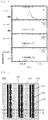
- FIG. 11 is a schematic view showing an example of the back surface of the back contact solar cell
- FIG. 12 shows a part of a cross section taken along an alternate long and short dash line A in FIG. 11 .
- an emitter region (an emitter layer) 1112 is formed on the back surface (a first main surface) of a semiconductor substrate (e.g., a crystal silicon substrate) 1110.
- base regions (base layers) 1113 are formed in a stripe pattern to sandwich the emitter region 1112 therebetween
- emitter electrodes 1122 are formed on the emitter region 1112, and further a plurality of emitter electrodes 1122 are coupled through emitter bus bars (emitter bus bar electrodes) 1132.
- base electrodes 1123 are formed on the base regions 1113, and a plurality of base electrodes 1123 are coupled through base bus bars (base bus bar electrodes) 1133.
- the base electrodes 1123 are electrically insulated from the emitter region 1112 through insulator films (insulator layers) 1118 and the emitter electrodes 1122 are electrically insulated from the base regions 1113 through the same.
- the solar cell 1100 includes passivation films 1119 on the first main surface and a second main surface of the semiconductor substrate 1110. It is to be noted that the passivation film 1119 is omitted in FIG. 11 .
- a material used for the insulator films must have characteristics such as chemical stableness, high usable temperatures, or easiness of pattern formation.
- a polyimide resin has been often used for the insulator film due to such demands (e.g., Patent Literature 1).
- the insulator film of the solar cell is formed by applying an insulation precursor (an insulator film precursor) to the substrate by screen printing, inkjet printing, or a dispensing method.
- an insulation precursor an insulator film precursor
- a solution containing a polyamic acid is generally used as a precursor in case of applying a polyimide resin for formation.
- the polyamic acid is thermally treated to advance dehydration reaction and imidization, whereby the polyimide resin is provided.
- Patent Literature 1 Japanese Unexamined Patent Application Publication No. 2015-26858
- the present invention has been made in view of the above problems, and an object thereof is to provide a solar cell which has excellent weather resistance and high photoelectric conversion characteristics and a method for manufacturing such a solar cell.
- the present invention provides a solar cell comprising: a semiconductor substrate having a first conductivity type; an emitter region, having a second conductivity type opposite to the first conductivity type, on a first main surface of the semiconductor substrate; an emitter electrode which is in contact with the emitter region; a base region having the first conductivity type; a base electrode which is in contact with the base region; and an insulator film for preventing an electrical short-circuit between the emitter region and the base region, wherein
- Such a solar cell is superior in weather resistance and has high photoelectric conversion characteristics.
- the insulator film is formed to electrically insulate the emitter region from the base electrode.
- Such a solar cell can avoid the electrical short-circuit of the emitter region and the base electrode by using the insulator film.
- the insulator film is formed to electrically insulate the base region from the emitter electrode.
- Such a solar cell can avoid the electrical short-circuit of the base region and the emitter electrode by using the insulator film.
- the insulator film is formed to electrically insulate the emitter electrode from the base electrode.
- Such a solar cell can avoid the electrical short-circuit of the emitter electrode and the base electrode by using the insulator film.
- the semiconductor substrate is a crystal silicon substrate.
- the semiconductor substrate is the crystal silicon substrate
- the solar cell which has good power generation efficiency can be provided at low cost.
- the present invention provides a photovoltaic module including solar cells according to the present invention electrically connected to each other.
- the solar cells according to the present invention can be electrically connected to provide the photovoltaic module.
- the present invention provides a photovoltaic power generation system including a plurality of photovoltaic modules according to the present invention connected to each other.
- the plurality of photovoltaic modules each of which is constituted by electrically connecting the solar cells according to the present invention can be connected to provide the photovoltaic power generation system.
- the present invention provides a method for manufacturing a solar cell comprising the steps of:
- a crystal silicon substrate as the semiconductor substrate.
- the method according to the present invention is particularly preferable for manufacture of the solar cell including the crystal silicon substrate.
- the solar cell of the present invention is superior in weather resistance and has high photoelectric conversion characteristics. According to the method of the present invention, it is possible to provide a back contact solar cell which has high efficiency and excellent weather resistance without requiring a process change.
- a solar cell including: a semiconductor substrate having a first conductivity type; an emitter region, having a second conductivity type opposite to the first conductivity type, on a first main surface of the semiconductor substrate; an emitter electrode which is in contact with the emitter region; a base region having the first conductivity type; a base electrode which is in contact with the base region; and an insulator film for preventing an electrical short-circuit between the emitter region and the base region, wherein the insulator film is made of a polyimide, and the insulator film has a C 6 H 11 O 2 detection count number of 100 or less when the insulator film is irradiated with Bi 5 ++ ions at an acceleration voltage of 30 kV and an ion current of 0.2 pA by a TOF-SIMS method, thereby bringing the present invention to completion.
- the present inventors have conducted the earnest examinations to achieve the object. Consequently, they have found that the problem can be solved by a method for manufacturing a solar cell including the steps of:
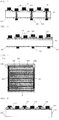
- FIG. 1 is a view showing a backside structure of a back contact solar cell according to the present invention.
- FIG. 2 is a view showing a cross-sectional structure of the back contact solar cell according to the present invention, and shows a part of a cross section taken along an alternate long and short dash line A in FIG. 1 .
- a solar cell 100 according to the present invention includes a semiconductor substrate 110 having a first conductivity type.
- an emitter region 112 having a second conductivity type opposite to the first conductivity type emitter electrodes 122 which are in contact with the emitter region 112
- base regions 113 having the first conductivity type base electrodes 123 which are in contact with the base regions 113
- insulator films 118 which prevent an electrical short-circuit between the emitter region 112 and the base regions 113.
- the solar cell 100 usually includes base bus bars 133 configured to further collect currents which can be provided from the base electrodes 123. Additionally, it usually includes emitter bus bars 132 configured to further collect currents which can be provided from the emitter electrodes 122. Further, as shown in FIG. 2 , passivation films 119 are usually provided on the first main surface and a second main surface of the semiconductor substrate 110. It is to be noted that the passivation film 119 is omitted in FIG. 1 .
- the insulator film 118 is made of a polyimide and has a C 6 H 11 O 2 detection count number of 100 or less when the insulator film 118 is irradiated with Bi 5 ++ ions (divalent ions of a bismuth pentamer) at an acceleration voltage of 30 kV and an ion current of 0.2 pA (picoampere) by a time-of-flight secondary ion mass spectrometry (TOF-SIMS) method.
- This detection count number is approximately a detection lower limit of the TOF-SIMS.
- an organic substance containing a carboxy group can be detected as, e.g., a peak of C 6 H 11 O 2 whose m/z value (m: an ion mass number, z: an ion charge number) appears in the vicinity of 115 in secondary ions ejected by Bi ion irradiation in the TOS-SIMS.
- each insulator film is made of a polyimide which hardly contains carboxy groups or does not contain the same at all.
- a carboxylic acid is generated from the carboxy group derived from an amic acid with moisture absorption of the insulator film and acts on electrodes themselves or an interface between the electrodes and silicon to degrade electric resistance.
- the shape of the insulator film is not restricted in particular, it may be, e.g., a rectangular shape.
- the length of one side of the insulator film may be, e.g., 0.01 mm to 50 mm.
- the thickness of the insulator film may be, e.g., 1 to 60 ⁇ m. Adopting such length and thickness enables further improving insulation properties.
- the insulator films are not excessively formed, it is possible to assuredly manufacture a desired solar cell, namely, a solar cell in which each insulator film is made of a polyimide containing no carboxy group.
- the solar cell 100 it is preferable to form the solar cell 100 according to the present invention so that the insulator films 118 electrically insulate the emitter region 112 from the base electrodes 123.
- the insulator films 118 electrically insulate the emitter region 112 from the base electrodes 123.
- Such a solar cell enables avoiding an electrical short-circuit between the emitter region and the base electrodes by using the insulator films.
- the solar cell 100 it is preferable to form the solar cell 100 according to the present invention so that the insulator films 118 electrically insulate the base regions 113 from the emitter electrodes 122.
- Such a solar cell enables avoiding an electrical short-circuit between the base regions and the emitter electrodes.
- the solar cell 100 it is preferable to form the solar cell 100 according to the present invention so that the insulator films 118 electrically insulate the emitter electrodes 122 from the base electrodes 123.
- Such a solar cell enables avoiding an electrical short-circuit between the emitter electrodes and the base electrodes.
- the semiconductor substrate 110 is a crystal silicon substrate.
- the semiconductor substrate is the crystal silicon substrate in this manner, the solar cell with the good power generation efficiency can be provided at low costs.
- the method according to the present invention can be applied to general solar cells using insulators, an example of the method will now be described.
- the method according to the present invention can be applied to the solar cell shown in FIGS. 1 and 2 .
- a specific method for manufacturing a solar cell will be described with reference to FIGS. 1 and 2 in conjunction with a case using an N-type substrate.
- an N-type semiconductor substrate such as an N-type crystal silicon substrate is prepared.
- high-purity silicon may be doped with a pentad such as phosphorous, arsenic, or antimony to prepare an as-cut single crystal ⁇ 100 ⁇ N-type silicon substrate having a specific resistance of 0.1 to 5 ⁇ cm.
- small irregularities called a texture may be formed on a light receiving surface of the semiconductor substrate to reduce reflectance of the solar cell.
- an emitter region 112 having a second conductivity type opposite to that of the semiconductor substrate 110 and base regions 113 having a first conductivity type equal to that of the semiconductor substrate 110 are formed on the back surface (a first main surface) of the semiconductor substrate 110.
- a method for forming the emitter region 112 and the base regions 113 is not restricted in particular, and a well-known method can be used.
- the emitter region 112 can be formed by vapor phase diffusion using BBr 3 or the like.
- the base regions 113 can be formed by vapor phase diffusion using phosphorous oxychloride.
- a diffusion mask composed of a silicon oxide film, a silicon nitride film, or the like may be used to form the emitter region 112 and the base regions 113 with desired shapes.
- a diffusion mask composed of a silicon oxide film, a silicon nitride film, or the like may be used to form the emitter region 112 and the base regions 113 with desired shapes.
- stripe-shaped base regions 113 may be formed, while emitter region 112 are formed except for areas where the base regions 113 are formed.
- a passivation film 119 constituted of a silicon nitride film, a silicon oxide film, or the like is formed on each of the light receiving surface and the back surface of the semiconductor substrate 110.
- the silicon nitride film can be formed by a CVD method, and the silicon oxide film can be formed by the CVD method or a thermal oxidation method.
- emitter electrodes 122 which are in contact with the emitter region 112, and base electrodes 123 which are in contact with the base regions 113 are formed.
- the emitter electrodes 122 and the base electrodes 123 which extend in a horizontal direction are formed on the emitter region 112 and the base regions 113.
- the emitter electrodes 122 and the base electrodes 123 are formed as follows: an Ag paste obtained by mixing Ag powder and glass frit with an organic binder is applied to the emitter region 112 and the base regions 113 with the passivation film 119 being inserted; the Ag paste is then dried; and the Ag paste is fired at about 700 to 880°C for 1 to 30 minutes. As a result of this heat treatment, the passivation film 119 is eroded by the Ag paste, whereby the electrodes make electrical contact with the silicon.
- plating may be applied.
- the passivation film 119 at such positions is removed by, e.g., laser ablation.
- the insulator films 118 for preventing an electrical short-circuit between the emitter region 112 and the base regions 113.
- the insulator films 118 are formed at intersecting points of the emitter region 112 and base bus bars 133 and intersecting points of the base regions 113 and emitter bus bars 132.
- the film is preferably formed by applying a paste of an insulation precursor by screen printing, inkjet printing, or dispensed coating in terms of productivity.
- a process differs to some extent depending on the insulation precursor to be used, it is often the case that the precursor is printed and thereafter dried in the air at approximately 70°C to 150°C for approximately one minute to 10 minutes, and then an actual curing is performed.
- an actual curing method also varies depending on the insulation precursor, it may be a thermosetting type, a UV (ultraviolet) curing type, or the like.
- heat treatment conditions for performing the actual curing for example, heat treatment can be carried out in the air at 200°C to 400°C for approximately 10 seconds to 15 minutes.
- each insulator film 118 is made of a polyimide containing no carboxy group.
- an organic substance containing carboxy groups can be detected as, e.g., a peak of C 6 H 11 O 2 whose m/z value (m: an ion mass number, z: an ion charge number) appears in the vicinity of 115 in secondary ions ejected by Bi ion irradiation in the TOS-SIMS.
- an actually cured insulator film having a C 6 H 11 O 2 detection count number of 100 or less when it is irradiated with Bi 5 ++ ions at an acceleration voltage of 30 kV and an ion current of 0.2 pA by the TOF-SIMS method can be regarded as the insulator film made of a polyimide containing no carboxy group. It is to be noted that the detection count number (100) is roughly a detection lower limit of the TOF-SIMS method.
- an amic acid solution is dehydrated/imidized by heat treatment, but imidization is partially incomplete due to a coating film thickness, heat treatment conditions, or the like, and the precursor remains in some situations. In such a case, there is a possibility that optimizing the coating film thickness and the heat treatment conditions can avoid the problem.
- an insulator film precursor containing no amic acid it is preferable to use an insulator film precursor containing no amic acid.
- a soluble polyimide coating agent using a soluble polyimide described in Japanese Unexamined Patent Application Publication No. 2015-180721 can be adopted.
- the soluble polyimide is, e.g., a polyimide powder provided by a solid phase polymerization method, and this polyimide can be the polyimide powder which is soluble in an amide solvent and whose weight-average molecular weight based on GPC (gel permeation chromatography) is 10000 or more.
- GPC gel permeation chromatography
- amide solvent examples include N-methyl-2-pyrolidone (NMP), N,N-dimethylformamide (DMF), N,N-dimethylacetamide (DMAc), and the like.
- the polyimide powder can be manufactured by solid-phase-polymerizing a salt consisting of a tetracarboxylic acid or a tetracarboxylic diester and diamine in the presence of a solvent in an amount of 1 mass% or more and 30 mass% or less with respect to a mass of this salt.
- the solid phase polymerization method is a method for advancing polymerization reaction in a solid state.
- the tetracarboxylic diester means a tetracarboxylic acid dimethyl ester, a tetracarboxylic acid diethyl ester, a tetracarboxylic diisopropyl acid ester, or the like.
- tetracarboxylic acid examples include cyclohexane-1,2,4,5-tetracarboxylic acid (H-PMA), pyromellitic acid (PMA), 3,3',4,4'-biphenyltetracarboxylic acid (BPA), 2,2-bis(3,4-dicarboxyphenyl) hexafluoropropane (6-FA), diesters of these substances, and the like.
- H-PMA cyclohexane-1,2,4,5-tetracarboxylic acid
- PMA pyromellitic acid
- BPA 3,3',4,4'-biphenyltetracarboxylic acid
- 6-FA 2,2-bis(3,4-dicarboxyphenyl) hexafluoropropane
- diamine examples include 4,4'-diaminodiphenyl ether (DADE), 2,2-bis[4-(4-aminophenyxy)phenyl]propane (BAPP), 1,3-bis(aminomethyl) cyclohexane (AMC), isophoronediamine (IPDA), 2,2-bis[4-(4-aminophenoxy)phenyl]hexafluoropropane (6F-BAPP), polypropylene glycol bis(2-aminoethyl) ether (PGAE), and the like.
- DADE 4,4'-diaminodiphenyl ether
- BAPP 2,2-bis[4-(4-aminophenyxy)phenyl]propane
- AMC 1,3-bis(aminomethyl) cyclohexane
- IPDA isophoronediamine
- 6F-BAPP 2,2-bis[4-(4-aminophenoxy)phenyl]hexafluoroprop
- the solvent used in the solid phase polymerization is a solvent which can dissolve the polyimide powder to be generated by the solid phase polymerization.
- Illustrative examples thereof include general solvents such as an amide solvent, an ether solvent, a water ester solvent, a ketone solvent, and the like; and the amide solvent is preferred.
- As the amide solvent, NMP, DMF, DMAc, or the like described above can be used.
- the sample A is an amic acid type polyimide film that is cured by, after coating and drying at 90°C for five minutes, heat treatment at 250°C for 10 minutes.
- the samples B to D are polyimide films made of soluble polyimides having different compositions, but a peak derived from the amic acid, which can be seen in the sample A, cannot be observed in these samples.
- Table 1 shows the details of the insulator films A, B, C, and D.
- Insulator film Film thickne ss Heat treatment conditions
- Type of insulator film precursor C 6 H 11 O 2 detection count number
- Solvent Others A about 20 ⁇ m drying at 90°C for 5 minutes, curing at 250°C for 10 minutes
- Amic acid solution about 1600 30 67 3
- the emitter bus bars 132 and the base bus bars 133 are formed.
- a thermosetting conductive paste which is curable at room temperature to 350°C or a UV curable conductive paste can be used for these bus bars, and such a paste could be applied by screen printing or dispenser formation.
- the insulator films 118 can electrically insulate the emitter electrodes 122 from the base bus bars 133 and also electrically insulate the base electrodes 123 from the emitter bus bars 132, while the emitter electrodes 122 and the emitter bus bars 132 can be configured to be electrically continuous, and the base electrodes 123 and the base bus bars 133 can be configured to be electrically continuous.
- the method of the present invention it is possible to provide a back contact solar cell having excellent durability and high efficiency.
- the foregoing examples are in conjunction with the case where the substrate is an N-type substrate, the method of the present invention can also be applied to a case where the substrate is a P-type substrate. That is, an N-type layer may be provided as an emitter layer while a P-type layer may be provided as a base layer.
- FIG. 4 is a view showing a back surface of an emitter-wrap-through solar cell 400 as a solar cell according to another embodiment of the present invention, and each of FIG. 5 (a cross-sectional view taken along an alternate long and short dash line A) and FIG. 6 (a cross-sectional view taken along an alternate long and short dash line B) shows a part of a cross section taken along the alternate long and short dash line A or B in FIG. 4 .
- the light receiving surface faces downward.
- a base region 113 and base electrodes 123 formed on the base region 113 most part of the back surface of a substrate 110 is occupied by a base region 113 and base electrodes 123 formed on the base region 113, and emitter regions 112 are formed into island shapes in regions sandwiched between insulator films 118.
- a light receiving surface is occupied by an emitter region 112 that communicates with the emitter regions 112 on the back surface through via holes opened in the substrate 110.
- emitter electrodes 122 are connected between the light-receiving surface and the back surface through the via holes.
- a passivation film 119 is formed on the light receiving surface.
- base bus bars 133 are linearly formed on the base electrode 123 on the back surface of the substrate 110.
- emitter bus bars 132 are linearly formed on the emitter regions 112 and the emitter electrodes 122 on the back surface of the substrate 110. However, as shown in FIG. 6 , in each region where the emitter bus bar 132 crosses the base electrode 123, the base electrode 123 is covered with the insulator film 118.
- FIG. 7 is a view showing the back surface of a solar cell 700 of still another embodiment according to the present invention
- FIG. 8 is a cross-sectional view showing a part of a cross section taken along an alternate long and short dash line A in FIG. 7
- base regions 113 on the back surface of a substrate 110 are formed in such a manner that they are surrounded by an emitter region 112, and each base electrode 123 is in contact with the base region 113 and insulated from a passivation film 119 through an insulator film 118 in a portion where the base electrode 123 overlaps the emitter region 112.
- the passivation film 119 is omitted in FIG. 7 . Additionally, at an outer peripheral portion of the back surface of the substrate 110, an emitter bus bar 132 which is coupled with a plurality of emitter electrodes 122 is formed, and a base bus bar 133 which is coupled with a plurality of base electrodes 123 is formed.
- each base region 113 is linearly formed below the base electrode 123, but the present invention is not restricted thereto, each base region 113 may be formed into a dot shape and these regions may be linearly aligned.
- the base electrodes 123 are formed in such a manner that they are insulated from the emitter region 112 through the insulator films 118 and connect the base regions 113.
- a photovoltaic module according to the present invention is constituted by electrically connecting the solar cells according to the present invention.
- a photovoltaic module is provided.
- FIG. 9 shows an example of a photovoltaic module 916.
- a positive electrode 923 of a solar cell is electrically connected to a negative electrode 922 of an adjacent solar cell through a tab 912, and the number of solar cells (solar battery cells) 900 required for a predetermined output are connected.
- the connected solar cells 900 are sealed with a cover glass, a filter, and further a back sheet.
- a soda-lime glass is extensively used.
- the filler ethylene vinyl acetate, polyolefin, silicone, or the like is used.
- the back sheet a functional film using polyethylene terephthalate is generally adopted.
- the positive electrode 923 of one solar cell is connected with a positive electrode terminal 913 of the photovoltaic module 916, and the negative electrode 922 of another solar cell is connected with a negative electrode terminal 914 of the photovoltaic module 916.
- a photovoltaic power generation system is constituted by connecting a plurality of photovoltaic modules according to the present invention.
- FIG. 10 shows a basic structure of a photovoltaic power generation system provided by coupling the modules of the present invention with each other. As shown in FIG. 10 , a plurality of photovoltaic modules 1016 are coupled in series through wiring 1015 and supply generated power to an external load circuit 1018 via an inverter 1017. Although not shown in this drawing, this system may further include a secondary battery which stores the generated power.
- a solar cell shown in FIGS. 1 and 2 was manufactured by using the method according to the present invention.
- an emitter region and base regions were formed on the back surface of the substrate as shown in FIG. 1 .
- This substrate was thermally treated in an oxygen atmosphere at 900°C for 10 minutes, and oxide silicon films were formed on both surfaces of the substrate. Subsequently, silicon nitride films with a film thickness of 90 nm were further formed on both the surfaces of the substrate by plasma CVD.
- an Ag paste was applied to the emitter region and the base regions by screen printing, and heat treatment was performed at 800°C for three seconds to cure the Ag paste, thereby forming emitter electrodes and base electrodes.
- an insulator film B in FIG. 3 was formed on a part of the emitter region and a part of the base electrode by screen printing. It is to be noted that conditions and others for forming the insulator film B are as described in Table 1.
- thermosetting Ag paste was applied by screen printing, and a heat treatment was performed at 200°C for five minutes to cure the paste, thereby providing a solar cell.
- Conductive wires are soldered to the bus bars in the solar cell and sealed with a white glass plate, a silicon resin, and a back sheet to fabricate a single cell module.
- Initial output characteristics of the manufactured single cell module were measured by using pseudo sunlight of a xenon lamp light source type, then the module was stored in a temperature and humidity testing chamber set to 85°C and 85% relative humidity for 2000 hours, and thereafter the measurement was again performed.
- an insulator film C in FIG. 3 was used to manufacture a solar cell. It is to be noted that conditions and others for forming the insulator film C are as described in Table 1.
- Initial output characteristics of the manufactured single cell module were measured by using pseudo sunlight of a xenon lamp light source type, then the module was stored in a temperature and humidity testing chamber set to 85°C and 85% relative humidity for 2000 hours, and thereafter the measurement was again performed.
- an insulator film A in FIG. 3 was applied to manufacture a solar cell. It is to be noted that conditions and others for forming the insulator film A are as described in Table 1.
- Initial output characteristics of the manufactured single cell module were measured by using pseudo sunlight of a xenon lamp light source type, then the module was stored in a temperature and humidity testing chamber set to 85°C and 85% relative humidity for 2000 hours, and thereafter the measurement was again performed.
- Table 2 shows the solar cell initial characteristics and characteristic decreasing rate after elapse of 2000 hours of the high temperature and high humidity test according to Examples 1 and 2 and Comparative Example 1 described above.
- Table 2 Solar cell characteristics Example 1
- Example 2 Comparative Example 1 Short-circuit current [mA/cm 2 ] Initial stage 39.4 39.5 39.4 After 2000 hours (decreasing rate %) 39.4 (0.0) 39.4 (0.3) 38.2 (3.0) Open circuit voltage [V] Initial stage 0.680 0.679 0.679 After 2000 hours (decreasing rate %) 0.680 (0.0) 0.680 (-0.1) 0.679 (0.0) Fill factor [%] Initial stage 80.9 80.7 81.0 After 2000 hours (decreasing rate %) 80.5 (0.5) 80.5 (0.2) 72.0 (11.1) Conversion efficiency [%] Initial stage 21.7 21.6 21.7 After 2000 hours (decreasing rate %) 21.6 (0.5) 21.6 (0.4) 18.7 (13.8)
- Example 1 and Example 2 As shown in Table 2, the initial characteristics of each of Example 1 and Example 2 (examples where the polyimide containing no carboxy group was formed as the insulator film) were comparable to those of Comparative Example 1 (an example where the polyimide containing carboxy groups was formed as the insulator film), but had greatly improved durability. This result shows that the solar cell with high efficiency and high weather resistance can be achieved by the present invention without requiring any additional step.
Landscapes
- Chemical & Material Sciences (AREA)
- Health & Medical Sciences (AREA)
- Organic Chemistry (AREA)
- Chemical Kinetics & Catalysis (AREA)
- Polymers & Plastics (AREA)
- Medicinal Chemistry (AREA)
- Life Sciences & Earth Sciences (AREA)
- Physics & Mathematics (AREA)
- Engineering & Computer Science (AREA)
- Biochemistry (AREA)
- Immunology (AREA)
- Pathology (AREA)
- General Physics & Mathematics (AREA)
- General Health & Medical Sciences (AREA)
- Molecular Biology (AREA)
- Analytical Chemistry (AREA)
- Spectroscopy & Molecular Physics (AREA)
- Sustainable Energy (AREA)
- Photovoltaic Devices (AREA)
- Sustainable Development (AREA)
- Manufacturing & Machinery (AREA)
- Crystallography & Structural Chemistry (AREA)
Applications Claiming Priority (1)
| Application Number | Priority Date | Filing Date | Title |
|---|---|---|---|
| PCT/JP2016/004884 WO2018092172A1 (fr) | 2016-11-15 | 2016-11-15 | Cellule solaire à haut rendement et procédé de fabrication de cellule solaire à haut rendement |
Publications (3)
| Publication Number | Publication Date |
|---|---|
| EP3349251A1 true EP3349251A1 (fr) | 2018-07-18 |
| EP3349251A4 EP3349251A4 (fr) | 2018-11-07 |
| EP3349251B1 EP3349251B1 (fr) | 2020-04-22 |
Family
ID=62146310
Family Applications (1)
| Application Number | Title | Priority Date | Filing Date |
|---|---|---|---|
| EP16886815.6A Active EP3349251B1 (fr) | 2016-11-15 | 2016-11-15 | Cellule solaire à haut rendement et procédé de fabrication de cellule solaire à haut rendement |
Country Status (7)
| Country | Link |
|---|---|
| US (2) | US10998463B2 (fr) |
| EP (1) | EP3349251B1 (fr) |
| JP (1) | JPWO2018092172A1 (fr) |
| KR (1) | KR102623721B1 (fr) |
| CN (1) | CN110073499B (fr) |
| TW (2) | TWI708400B (fr) |
| WO (1) | WO2018092172A1 (fr) |
Families Citing this family (2)
| Publication number | Priority date | Publication date | Assignee | Title |
|---|---|---|---|---|
| JP6741626B2 (ja) * | 2017-06-26 | 2020-08-19 | 信越化学工業株式会社 | 高効率裏面電極型太陽電池及びその製造方法 |
| CN120547982A (zh) * | 2023-03-31 | 2025-08-26 | 天合光能股份有限公司 | 太阳电池及太阳电池的制备方法 |
Family Cites Families (30)
| Publication number | Priority date | Publication date | Assignee | Title |
|---|---|---|---|---|
| JPH01129233A (ja) | 1987-11-13 | 1989-05-22 | Toppan Printing Co Ltd | 表示装置用電極板の製造方法 |
| JPH068036B2 (ja) * | 1988-09-28 | 1994-02-02 | 株式会社日立製作所 | 金属/ポリイミド複合体の製造方法 |
| US5120573A (en) | 1988-09-28 | 1992-06-09 | Hitachi, Ltd. | Process for producing metal/polyimide composite article |
| JP2713052B2 (ja) | 1992-08-26 | 1998-02-16 | 信越化学工業株式会社 | ポリイミド樹脂溶液組成物及びコーティング剤 |
| US5738931A (en) | 1994-09-16 | 1998-04-14 | Kabushiki Kaisha Toshiba | Electronic device and magnetic device |
| JP3544758B2 (ja) | 1994-09-16 | 2004-07-21 | 株式会社東芝 | 電子部品および磁気部品 |
| JPH104263A (ja) | 1996-06-17 | 1998-01-06 | Hitachi Ltd | 電子回路基板及びその製造方法 |
| JPH10171116A (ja) | 1996-12-12 | 1998-06-26 | Hitachi Ltd | ポジ型感光性樹脂組成物とそれを用いたポリイミド膜の形成法 |
| JPH1152572A (ja) | 1997-08-08 | 1999-02-26 | Fujitsu Ltd | 感光性樹脂組成物及びそれを用いたパターン形成方法 |
| US6586081B1 (en) | 1999-03-12 | 2003-07-01 | Kaneka Corporation | Polyimide/metal laminate, and electric/electronic equipment bases, magnetic recording bases, solar battery bases, coating film for aerospace materials and filmy resistance elements with the use thereof |
| JP2007131005A (ja) * | 1999-03-12 | 2007-05-31 | Kaneka Corp | ポリイミド/金属積層体並びにそれを用いた電気・電子機器用基盤、磁気記録用基盤、太陽電池用基盤、宇宙空間航行用機材の被覆フィルム、及びフィルム状抵抗体 |
| JP2006203056A (ja) | 2005-01-21 | 2006-08-03 | Toyota Motor Corp | 光電変換素子 |
| US8008575B2 (en) | 2006-07-24 | 2011-08-30 | Sunpower Corporation | Solar cell with reduced base diffusion area |
| JP5090716B2 (ja) * | 2006-11-24 | 2012-12-05 | 信越化学工業株式会社 | 単結晶シリコン太陽電池の製造方法 |
| JP5428442B2 (ja) * | 2008-03-31 | 2014-02-26 | 大日本印刷株式会社 | ポリイミド前駆体、ポリイミド前駆体樹脂組成物、及び電子部品 |
| US8071273B2 (en) | 2008-03-31 | 2011-12-06 | Dai Nippon Printing Co., Ltd. | Polyimide precursor, resin composition comprising the polyimide precursor, pattern forming method using the resin composition, and articles produced by using the resin composition |
| JP2009253096A (ja) | 2008-04-08 | 2009-10-29 | Sharp Corp | 太陽電池セルの製造方法および太陽電池モジュールの製造方法ならびに太陽電池モジュール |
| TWI392405B (zh) * | 2009-10-26 | 2013-04-01 | Unimicron Technology Corp | 線路結構 |
| JP2012069594A (ja) * | 2010-09-21 | 2012-04-05 | Pi R & D Co Ltd | 太陽電池内の絶縁膜形成用ポリイミド樹脂組成物及びそれを用いた太陽電池内の絶縁膜形成方法 |
| WO2012057124A1 (fr) | 2010-10-25 | 2012-05-03 | ダイキン工業株式会社 | Stratifié métallisé, procédé de fabrication associé, et carte de circuit imprimé flexible |
| CN103534325B (zh) | 2011-03-31 | 2015-11-25 | 东洋油墨Sc控股株式会社 | 积层片用接着剂组合物及太阳电池用背面保护片 |
| KR101644680B1 (ko) | 2011-04-28 | 2016-08-01 | 후지필름 가부시키가이샤 | 도전성 부재, 그 제조 방법, 터치 패널 및 태양 전지 |
| TW201318869A (zh) | 2011-09-16 | 2013-05-16 | Mitsubishi Plastics Inc | 太陽電池用保護材 |
| CN104769021B (zh) * | 2012-11-08 | 2017-10-10 | 旭化成株式会社 | 柔性器件用基板、柔性器件及其制造方法、层积体及其制造方法、以及树脂组合物 |
| US9112100B2 (en) * | 2014-01-20 | 2015-08-18 | Sandia Corporation | Method for fabricating pixelated silicon device cells |
| JP2015180721A (ja) * | 2014-03-03 | 2015-10-15 | ユニチカ株式会社 | ポリイミドおよびその製造方法 |
| EP3157062B1 (fr) | 2014-06-11 | 2023-12-20 | Shin-Etsu Chemical Co., Ltd. | Cellule solaire et procédé de fabrication de cellule solaire |
| JP6199839B2 (ja) | 2014-09-30 | 2017-09-20 | 信越化学工業株式会社 | 太陽電池及びその製造方法 |
| JP6141342B2 (ja) * | 2015-02-05 | 2017-06-07 | 信越化学工業株式会社 | 裏面接合型太陽電池 |
| KR102556599B1 (ko) * | 2016-11-07 | 2023-07-17 | 신에쓰 가가꾸 고교 가부시끼가이샤 | 고효율 태양전지의 제조 방법 |
-
2016
- 2016-11-15 EP EP16886815.6A patent/EP3349251B1/fr active Active
- 2016-11-15 KR KR1020197013773A patent/KR102623721B1/ko active Active
- 2016-11-15 CN CN201680090769.4A patent/CN110073499B/zh active Active
- 2016-11-15 WO PCT/JP2016/004884 patent/WO2018092172A1/fr not_active Ceased
- 2016-11-15 US US16/346,907 patent/US10998463B2/en active Active
- 2016-11-15 JP JP2017519703A patent/JPWO2018092172A1/ja active Pending
-
2017
- 2017-03-07 TW TW108100027A patent/TWI708400B/zh active
- 2017-03-07 TW TW106107411A patent/TWI649885B/zh active
-
2021
- 2021-04-05 US US17/222,281 patent/US11552202B2/en active Active
Also Published As
| Publication number | Publication date |
|---|---|
| TWI649885B (zh) | 2019-02-01 |
| EP3349251A4 (fr) | 2018-11-07 |
| TW201933621A (zh) | 2019-08-16 |
| US20210226080A1 (en) | 2021-07-22 |
| US10998463B2 (en) | 2021-05-04 |
| KR102623721B1 (ko) | 2024-01-11 |
| TW201820644A (zh) | 2018-06-01 |
| JPWO2018092172A1 (ja) | 2018-11-15 |
| TWI708400B (zh) | 2020-10-21 |
| WO2018092172A1 (fr) | 2018-05-24 |
| CN110073499A (zh) | 2019-07-30 |
| CN110073499B (zh) | 2024-04-05 |
| KR20190082790A (ko) | 2019-07-10 |
| EP3349251B1 (fr) | 2020-04-22 |
| US11552202B2 (en) | 2023-01-10 |
| US20200058810A1 (en) | 2020-02-20 |
Similar Documents
| Publication | Publication Date | Title |
|---|---|---|
| KR102366908B1 (ko) | 태양전지 및 그 제조 방법 | |
| EP2184787A1 (fr) | Cellule solaire du type à connexion par la surface arrière, cellule solaire du type à connexion par la surface arrière ayant une carte de câblage, chaîne de cellules solaires et module de cellule solaire | |
| US20110030759A1 (en) | Method for manufacturing solar cell, method for manufacturing solar cell module, and solar cell module | |
| US11552202B2 (en) | High efficiency solar cell and method for manufacturing high efficiency solar cell | |
| CN102655030A (zh) | 导电组合物、含其的硅太阳能电池、及其制造方法 | |
| US20180097128A1 (en) | Solar cell device and method for manufacturing same | |
| EP3101696A1 (fr) | Pile solaire et son procédé de fabrication | |
| CN103765523A (zh) | 导电浆料、半导体装置用电极、半导体装置及半导体装置的制造方法 | |
| JP6532518B2 (ja) | 高効率太陽電池の製造方法 | |
| KR20180070499A (ko) | 태양광 모듈의 제조 방법 및 그 방법에 의해 얻어진 태양광 모듈 | |
| KR20120100698A (ko) | 전도성 조성물, 이를 포함하는 실리콘 태양전지 및 그 제조방법 | |
| TW200927850A (en) | Screen-printable encapsulants based on polyhydroxyamides that thermally convert to polybenzoxazoles | |
| EP3343643B1 (fr) | Procédé de fabrication de cellule solaire hautement efficace | |
| EP3702048B1 (fr) | Procédé de séchage d'une pâte de polyimide et procédé de production de cellules solaires aptes à une conversion photoélectrique très efficace | |
| US20120301998A1 (en) | Method for manufacturing solar cell | |
| Kyranaki et al. | Impact of encapsulation processing conditions on degradation mechanisms of carbon-based perovskite solar cells | |
| JP5392138B2 (ja) | 導電性組成物及びそれを用いた太陽電池の製造方法 | |
| JP6405285B2 (ja) | 太陽電池の製造方法 |
Legal Events
| Date | Code | Title | Description |
|---|---|---|---|
| STAA | Information on the status of an ep patent application or granted ep patent |
Free format text: STATUS: UNKNOWN |
|
| STAA | Information on the status of an ep patent application or granted ep patent |
Free format text: STATUS: THE INTERNATIONAL PUBLICATION HAS BEEN MADE |
|
| PUAI | Public reference made under article 153(3) epc to a published international application that has entered the european phase |
Free format text: ORIGINAL CODE: 0009012 |
|
| STAA | Information on the status of an ep patent application or granted ep patent |
Free format text: STATUS: THE APPLICATION HAS BEEN PUBLISHED |
|
| AK | Designated contracting states |
Kind code of ref document: A1 Designated state(s): AL AT BE BG CH CY CZ DE DK EE ES FI FR GB GR HR HU IE IS IT LI LT LU LV MC MK MT NL NO PL PT RO RS SE SI SK SM TR |
|
| AX | Request for extension of the european patent |
Extension state: BA ME |
|
| STAA | Information on the status of an ep patent application or granted ep patent |
Free format text: STATUS: REQUEST FOR EXAMINATION WAS MADE |
|
| A4 | Supplementary search report drawn up and despatched |
Effective date: 20181010 |
|
| RIC1 | Information provided on ipc code assigned before grant |
Ipc: H01L 31/0224 20060101ALI20181001BHEP Ipc: H01L 31/068 20120101ALI20181001BHEP Ipc: H01L 31/0216 20140101AFI20181001BHEP Ipc: C08G 73/10 20060101ALI20181001BHEP Ipc: H01L 31/042 20140101ALI20181001BHEP |
|
| 17P | Request for examination filed |
Effective date: 20181008 |
|
| GRAP | Despatch of communication of intention to grant a patent |
Free format text: ORIGINAL CODE: EPIDOSNIGR1 |
|
| STAA | Information on the status of an ep patent application or granted ep patent |
Free format text: STATUS: GRANT OF PATENT IS INTENDED |
|
| DAV | Request for validation of the european patent (deleted) | ||
| DAX | Request for extension of the european patent (deleted) | ||
| INTG | Intention to grant announced |
Effective date: 20191111 |
|
| GRAS | Grant fee paid |
Free format text: ORIGINAL CODE: EPIDOSNIGR3 |
|
| GRAA | (expected) grant |
Free format text: ORIGINAL CODE: 0009210 |
|
| STAA | Information on the status of an ep patent application or granted ep patent |
Free format text: STATUS: THE PATENT HAS BEEN GRANTED |
|
| RIN1 | Information on inventor provided before grant (corrected) |
Inventor name: HASHIGAMI, HIROSHI Inventor name: OHTSUKA, HIROYUKI Inventor name: MORIYAMA, SHUN Inventor name: WATABE, TAKENORI |
|
| AK | Designated contracting states |
Kind code of ref document: B1 Designated state(s): AL AT BE BG CH CY CZ DE DK EE ES FI FR GB GR HR HU IE IS IT LI LT LU LV MC MK MT NL NO PL PT RO RS SE SI SK SM TR |
|
| REG | Reference to a national code |
Ref country code: CH Ref legal event code: EP |
|
| REG | Reference to a national code |
Ref country code: IE Ref legal event code: FG4D |
|
| REG | Reference to a national code |
Ref country code: DE Ref legal event code: R096 Ref document number: 602016034814 Country of ref document: DE |
|
| REG | Reference to a national code |
Ref country code: AT Ref legal event code: REF Ref document number: 1261286 Country of ref document: AT Kind code of ref document: T Effective date: 20200515 |
|
| REG | Reference to a national code |
Ref country code: NL Ref legal event code: FP |
|
| REG | Reference to a national code |
Ref country code: LT Ref legal event code: MG4D |
|
| PG25 | Lapsed in a contracting state [announced via postgrant information from national office to epo] |
Ref country code: IS Free format text: LAPSE BECAUSE OF FAILURE TO SUBMIT A TRANSLATION OF THE DESCRIPTION OR TO PAY THE FEE WITHIN THE PRESCRIBED TIME-LIMIT Effective date: 20200822 Ref country code: FI Free format text: LAPSE BECAUSE OF FAILURE TO SUBMIT A TRANSLATION OF THE DESCRIPTION OR TO PAY THE FEE WITHIN THE PRESCRIBED TIME-LIMIT Effective date: 20200422 Ref country code: PT Free format text: LAPSE BECAUSE OF FAILURE TO SUBMIT A TRANSLATION OF THE DESCRIPTION OR TO PAY THE FEE WITHIN THE PRESCRIBED TIME-LIMIT Effective date: 20200824 Ref country code: SE Free format text: LAPSE BECAUSE OF FAILURE TO SUBMIT A TRANSLATION OF THE DESCRIPTION OR TO PAY THE FEE WITHIN THE PRESCRIBED TIME-LIMIT Effective date: 20200422 Ref country code: LT Free format text: LAPSE BECAUSE OF FAILURE TO SUBMIT A TRANSLATION OF THE DESCRIPTION OR TO PAY THE FEE WITHIN THE PRESCRIBED TIME-LIMIT Effective date: 20200422 Ref country code: NO Free format text: LAPSE BECAUSE OF FAILURE TO SUBMIT A TRANSLATION OF THE DESCRIPTION OR TO PAY THE FEE WITHIN THE PRESCRIBED TIME-LIMIT Effective date: 20200722 Ref country code: GR Free format text: LAPSE BECAUSE OF FAILURE TO SUBMIT A TRANSLATION OF THE DESCRIPTION OR TO PAY THE FEE WITHIN THE PRESCRIBED TIME-LIMIT Effective date: 20200723 |
|
| REG | Reference to a national code |
Ref country code: AT Ref legal event code: MK05 Ref document number: 1261286 Country of ref document: AT Kind code of ref document: T Effective date: 20200422 |
|
| PG25 | Lapsed in a contracting state [announced via postgrant information from national office to epo] |
Ref country code: BG Free format text: LAPSE BECAUSE OF FAILURE TO SUBMIT A TRANSLATION OF THE DESCRIPTION OR TO PAY THE FEE WITHIN THE PRESCRIBED TIME-LIMIT Effective date: 20200722 Ref country code: RS Free format text: LAPSE BECAUSE OF FAILURE TO SUBMIT A TRANSLATION OF THE DESCRIPTION OR TO PAY THE FEE WITHIN THE PRESCRIBED TIME-LIMIT Effective date: 20200422 Ref country code: HR Free format text: LAPSE BECAUSE OF FAILURE TO SUBMIT A TRANSLATION OF THE DESCRIPTION OR TO PAY THE FEE WITHIN THE PRESCRIBED TIME-LIMIT Effective date: 20200422 Ref country code: LV Free format text: LAPSE BECAUSE OF FAILURE TO SUBMIT A TRANSLATION OF THE DESCRIPTION OR TO PAY THE FEE WITHIN THE PRESCRIBED TIME-LIMIT Effective date: 20200422 |
|
| PG25 | Lapsed in a contracting state [announced via postgrant information from national office to epo] |
Ref country code: AL Free format text: LAPSE BECAUSE OF FAILURE TO SUBMIT A TRANSLATION OF THE DESCRIPTION OR TO PAY THE FEE WITHIN THE PRESCRIBED TIME-LIMIT Effective date: 20200422 |
|
| REG | Reference to a national code |
Ref country code: DE Ref legal event code: R097 Ref document number: 602016034814 Country of ref document: DE |
|
| PG25 | Lapsed in a contracting state [announced via postgrant information from national office to epo] |
Ref country code: AT Free format text: LAPSE BECAUSE OF FAILURE TO SUBMIT A TRANSLATION OF THE DESCRIPTION OR TO PAY THE FEE WITHIN THE PRESCRIBED TIME-LIMIT Effective date: 20200422 Ref country code: ES Free format text: LAPSE BECAUSE OF FAILURE TO SUBMIT A TRANSLATION OF THE DESCRIPTION OR TO PAY THE FEE WITHIN THE PRESCRIBED TIME-LIMIT Effective date: 20200422 Ref country code: DK Free format text: LAPSE BECAUSE OF FAILURE TO SUBMIT A TRANSLATION OF THE DESCRIPTION OR TO PAY THE FEE WITHIN THE PRESCRIBED TIME-LIMIT Effective date: 20200422 Ref country code: SM Free format text: LAPSE BECAUSE OF FAILURE TO SUBMIT A TRANSLATION OF THE DESCRIPTION OR TO PAY THE FEE WITHIN THE PRESCRIBED TIME-LIMIT Effective date: 20200422 Ref country code: EE Free format text: LAPSE BECAUSE OF FAILURE TO SUBMIT A TRANSLATION OF THE DESCRIPTION OR TO PAY THE FEE WITHIN THE PRESCRIBED TIME-LIMIT Effective date: 20200422 Ref country code: RO Free format text: LAPSE BECAUSE OF FAILURE TO SUBMIT A TRANSLATION OF THE DESCRIPTION OR TO PAY THE FEE WITHIN THE PRESCRIBED TIME-LIMIT Effective date: 20200422 Ref country code: IT Free format text: LAPSE BECAUSE OF FAILURE TO SUBMIT A TRANSLATION OF THE DESCRIPTION OR TO PAY THE FEE WITHIN THE PRESCRIBED TIME-LIMIT Effective date: 20200422 Ref country code: CZ Free format text: LAPSE BECAUSE OF FAILURE TO SUBMIT A TRANSLATION OF THE DESCRIPTION OR TO PAY THE FEE WITHIN THE PRESCRIBED TIME-LIMIT Effective date: 20200422 |
|
| PG25 | Lapsed in a contracting state [announced via postgrant information from national office to epo] |
Ref country code: SK Free format text: LAPSE BECAUSE OF FAILURE TO SUBMIT A TRANSLATION OF THE DESCRIPTION OR TO PAY THE FEE WITHIN THE PRESCRIBED TIME-LIMIT Effective date: 20200422 Ref country code: PL Free format text: LAPSE BECAUSE OF FAILURE TO SUBMIT A TRANSLATION OF THE DESCRIPTION OR TO PAY THE FEE WITHIN THE PRESCRIBED TIME-LIMIT Effective date: 20200422 |
|
| PLBE | No opposition filed within time limit |
Free format text: ORIGINAL CODE: 0009261 |
|
| STAA | Information on the status of an ep patent application or granted ep patent |
Free format text: STATUS: NO OPPOSITION FILED WITHIN TIME LIMIT |
|
| 26N | No opposition filed |
Effective date: 20210125 |
|
| PG25 | Lapsed in a contracting state [announced via postgrant information from national office to epo] |
Ref country code: SI Free format text: LAPSE BECAUSE OF FAILURE TO SUBMIT A TRANSLATION OF THE DESCRIPTION OR TO PAY THE FEE WITHIN THE PRESCRIBED TIME-LIMIT Effective date: 20200422 |
|
| PG25 | Lapsed in a contracting state [announced via postgrant information from national office to epo] |
Ref country code: MC Free format text: LAPSE BECAUSE OF FAILURE TO SUBMIT A TRANSLATION OF THE DESCRIPTION OR TO PAY THE FEE WITHIN THE PRESCRIBED TIME-LIMIT Effective date: 20200422 |
|
| REG | Reference to a national code |
Ref country code: CH Ref legal event code: PL |
|
| GBPC | Gb: european patent ceased through non-payment of renewal fee |
Effective date: 20201115 |
|
| PG25 | Lapsed in a contracting state [announced via postgrant information from national office to epo] |
Ref country code: LU Free format text: LAPSE BECAUSE OF NON-PAYMENT OF DUE FEES Effective date: 20201115 |
|
| REG | Reference to a national code |
Ref country code: BE Ref legal event code: MM Effective date: 20201130 |
|
| PG25 | Lapsed in a contracting state [announced via postgrant information from national office to epo] |
Ref country code: CH Free format text: LAPSE BECAUSE OF NON-PAYMENT OF DUE FEES Effective date: 20201130 Ref country code: LI Free format text: LAPSE BECAUSE OF NON-PAYMENT OF DUE FEES Effective date: 20201130 |
|
| PG25 | Lapsed in a contracting state [announced via postgrant information from national office to epo] |
Ref country code: IE Free format text: LAPSE BECAUSE OF NON-PAYMENT OF DUE FEES Effective date: 20201115 |
|
| PG25 | Lapsed in a contracting state [announced via postgrant information from national office to epo] |
Ref country code: GB Free format text: LAPSE BECAUSE OF NON-PAYMENT OF DUE FEES Effective date: 20201115 |
|
| PG25 | Lapsed in a contracting state [announced via postgrant information from national office to epo] |
Ref country code: TR Free format text: LAPSE BECAUSE OF FAILURE TO SUBMIT A TRANSLATION OF THE DESCRIPTION OR TO PAY THE FEE WITHIN THE PRESCRIBED TIME-LIMIT Effective date: 20200422 Ref country code: MT Free format text: LAPSE BECAUSE OF FAILURE TO SUBMIT A TRANSLATION OF THE DESCRIPTION OR TO PAY THE FEE WITHIN THE PRESCRIBED TIME-LIMIT Effective date: 20200422 Ref country code: CY Free format text: LAPSE BECAUSE OF FAILURE TO SUBMIT A TRANSLATION OF THE DESCRIPTION OR TO PAY THE FEE WITHIN THE PRESCRIBED TIME-LIMIT Effective date: 20200422 |
|
| PG25 | Lapsed in a contracting state [announced via postgrant information from national office to epo] |
Ref country code: MK Free format text: LAPSE BECAUSE OF FAILURE TO SUBMIT A TRANSLATION OF THE DESCRIPTION OR TO PAY THE FEE WITHIN THE PRESCRIBED TIME-LIMIT Effective date: 20200422 |
|
| PG25 | Lapsed in a contracting state [announced via postgrant information from national office to epo] |
Ref country code: BE Free format text: LAPSE BECAUSE OF NON-PAYMENT OF DUE FEES Effective date: 20201130 |
|
| P01 | Opt-out of the competence of the unified patent court (upc) registered |
Effective date: 20230512 |
|
| REG | Reference to a national code |
Ref country code: DE Ref legal event code: R079 Ref document number: 602016034814 Country of ref document: DE Free format text: PREVIOUS MAIN CLASS: H01L0031021600 Ipc: H10F0077300000 |
|
| PG25 | Lapsed in a contracting state [announced via postgrant information from national office to epo] |
Ref country code: IS Free format text: LAPSE BECAUSE OF NON-PAYMENT OF DUE FEES Effective date: 20200822 |
|
| PGFP | Annual fee paid to national office [announced via postgrant information from national office to epo] |
Ref country code: NL Payment date: 20251119 Year of fee payment: 10 |
|
| PGFP | Annual fee paid to national office [announced via postgrant information from national office to epo] |
Ref country code: DE Payment date: 20251119 Year of fee payment: 10 |
|
| PGFP | Annual fee paid to national office [announced via postgrant information from national office to epo] |
Ref country code: FR Payment date: 20251126 Year of fee payment: 10 |