EP3364248A1 - Elektronenstrahllithografieverfahren für eine probe mit mindestens einer zerbrechlichen nanostruktur - Google Patents
Elektronenstrahllithografieverfahren für eine probe mit mindestens einer zerbrechlichen nanostruktur Download PDFInfo
- Publication number
- EP3364248A1 EP3364248A1 EP17305169.9A EP17305169A EP3364248A1 EP 3364248 A1 EP3364248 A1 EP 3364248A1 EP 17305169 A EP17305169 A EP 17305169A EP 3364248 A1 EP3364248 A1 EP 3364248A1
- Authority
- EP
- European Patent Office
- Prior art keywords
- resist
- layer
- electron
- selected structure
- process according
- Prior art date
- Legal status (The legal status is an assumption and is not a legal conclusion. Google has not performed a legal analysis and makes no representation as to the accuracy of the status listed.)
- Withdrawn
Links
- 238000000034 method Methods 0.000 title claims abstract description 61
- 238000000609 electron-beam lithography Methods 0.000 title description 21
- 239000002086 nanomaterial Substances 0.000 title description 5
- 238000010894 electron beam technology Methods 0.000 claims abstract description 43
- 230000003287 optical effect Effects 0.000 claims abstract description 34
- 238000003384 imaging method Methods 0.000 claims abstract description 20
- 238000001459 lithography Methods 0.000 claims abstract description 18
- 230000005855 radiation Effects 0.000 claims abstract description 13
- 239000003550 marker Substances 0.000 claims abstract description 9
- IJGRMHOSHXDMSA-UHFFFAOYSA-N Atomic nitrogen Chemical compound N#N IJGRMHOSHXDMSA-UHFFFAOYSA-N 0.000 claims description 16
- 239000002096 quantum dot Substances 0.000 claims description 13
- 238000000206 photolithography Methods 0.000 claims description 9
- 239000002113 nanodiamond Substances 0.000 claims description 8
- 229910052757 nitrogen Inorganic materials 0.000 claims description 8
- 239000003989 dielectric material Substances 0.000 claims description 6
- 230000010287 polarization Effects 0.000 claims description 5
- 229920003229 poly(methyl methacrylate) Polymers 0.000 description 16
- 239000004926 polymethyl methacrylate Substances 0.000 description 16
- 238000002073 fluorescence micrograph Methods 0.000 description 12
- 229910052751 metal Inorganic materials 0.000 description 11
- 239000002184 metal Substances 0.000 description 11
- UHYPYGJEEGLRJD-UHFFFAOYSA-N cadmium(2+);selenium(2-) Chemical class [Se-2].[Cd+2] UHYPYGJEEGLRJD-UHFFFAOYSA-N 0.000 description 6
- 230000008901 benefit Effects 0.000 description 5
- 239000000463 material Substances 0.000 description 5
- 238000000386 microscopy Methods 0.000 description 5
- 238000000399 optical microscopy Methods 0.000 description 5
- 238000004626 scanning electron microscopy Methods 0.000 description 5
- 239000002904 solvent Substances 0.000 description 5
- 239000000126 substance Substances 0.000 description 5
- KFZMGEQAYNKOFK-UHFFFAOYSA-N Isopropanol Chemical compound CC(C)O KFZMGEQAYNKOFK-UHFFFAOYSA-N 0.000 description 4
- 238000012822 chemical development Methods 0.000 description 4
- 230000001066 destructive effect Effects 0.000 description 4
- 239000010931 gold Substances 0.000 description 4
- 230000003993 interaction Effects 0.000 description 4
- 238000005259 measurement Methods 0.000 description 4
- NTIZESTWPVYFNL-UHFFFAOYSA-N Methyl isobutyl ketone Chemical compound CC(C)CC(C)=O NTIZESTWPVYFNL-UHFFFAOYSA-N 0.000 description 3
- UIHCLUNTQKBZGK-UHFFFAOYSA-N Methyl isobutyl ketone Natural products CCC(C)C(C)=O UIHCLUNTQKBZGK-UHFFFAOYSA-N 0.000 description 3
- YXFVVABEGXRONW-UHFFFAOYSA-N Toluene Chemical compound CC1=CC=CC=C1 YXFVVABEGXRONW-UHFFFAOYSA-N 0.000 description 3
- 230000005540 biological transmission Effects 0.000 description 3
- 230000006378 damage Effects 0.000 description 3
- 238000005530 etching Methods 0.000 description 3
- 230000005284 excitation Effects 0.000 description 3
- 239000010408 film Substances 0.000 description 3
- 229910052737 gold Inorganic materials 0.000 description 3
- 238000004519 manufacturing process Methods 0.000 description 3
- VLKZOEOYAKHREP-UHFFFAOYSA-N n-Hexane Chemical compound CCCCCC VLKZOEOYAKHREP-UHFFFAOYSA-N 0.000 description 3
- 239000000758 substrate Substances 0.000 description 3
- HEDRZPFGACZZDS-UHFFFAOYSA-N Chloroform Chemical compound ClC(Cl)Cl HEDRZPFGACZZDS-UHFFFAOYSA-N 0.000 description 2
- 101000793686 Homo sapiens Azurocidin Proteins 0.000 description 2
- VYPSYNLAJGMNEJ-UHFFFAOYSA-N Silicium dioxide Chemical compound O=[Si]=O VYPSYNLAJGMNEJ-UHFFFAOYSA-N 0.000 description 2
- XUIMIQQOPSSXEZ-UHFFFAOYSA-N Silicon Chemical compound [Si] XUIMIQQOPSSXEZ-UHFFFAOYSA-N 0.000 description 2
- 238000000151 deposition Methods 0.000 description 2
- 230000008021 deposition Effects 0.000 description 2
- 238000001493 electron microscopy Methods 0.000 description 2
- 238000000799 fluorescence microscopy Methods 0.000 description 2
- PCHJSUWPFVWCPO-UHFFFAOYSA-N gold Chemical compound [Au] PCHJSUWPFVWCPO-UHFFFAOYSA-N 0.000 description 2
- 238000004020 luminiscence type Methods 0.000 description 2
- 238000001000 micrograph Methods 0.000 description 2
- 230000035515 penetration Effects 0.000 description 2
- 229910052710 silicon Inorganic materials 0.000 description 2
- 239000010703 silicon Substances 0.000 description 2
- 229910052709 silver Inorganic materials 0.000 description 2
- 238000012360 testing method Methods 0.000 description 2
- 241000519995 Stachys sylvatica Species 0.000 description 1
- 238000010521 absorption reaction Methods 0.000 description 1
- 229910052782 aluminium Inorganic materials 0.000 description 1
- 238000004140 cleaning Methods 0.000 description 1
- 229910052681 coesite Inorganic materials 0.000 description 1
- 238000007796 conventional method Methods 0.000 description 1
- 229910052906 cristobalite Inorganic materials 0.000 description 1
- 238000001514 detection method Methods 0.000 description 1
- 230000002542 deteriorative effect Effects 0.000 description 1
- 238000011161 development Methods 0.000 description 1
- 239000006185 dispersion Substances 0.000 description 1
- 230000005672 electromagnetic field Effects 0.000 description 1
- 239000011521 glass Substances 0.000 description 1
- 239000007788 liquid Substances 0.000 description 1
- QSHDDOUJBYECFT-UHFFFAOYSA-N mercury Chemical compound [Hg] QSHDDOUJBYECFT-UHFFFAOYSA-N 0.000 description 1
- 229910052753 mercury Inorganic materials 0.000 description 1
- 239000002159 nanocrystal Substances 0.000 description 1
- 238000012634 optical imaging Methods 0.000 description 1
- 238000005240 physical vapour deposition Methods 0.000 description 1
- 229910052697 platinum Inorganic materials 0.000 description 1
- 230000002265 prevention Effects 0.000 description 1
- 239000004065 semiconductor Substances 0.000 description 1
- 230000035945 sensitivity Effects 0.000 description 1
- 239000000377 silicon dioxide Substances 0.000 description 1
- 235000012239 silicon dioxide Nutrition 0.000 description 1
- 239000004332 silver Substances 0.000 description 1
- 238000001228 spectrum Methods 0.000 description 1
- 238000004528 spin coating Methods 0.000 description 1
- 229910052682 stishovite Inorganic materials 0.000 description 1
- 239000010409 thin film Substances 0.000 description 1
- 229910052905 tridymite Inorganic materials 0.000 description 1
- 238000007740 vapor deposition Methods 0.000 description 1
Images


Classifications
-
- B—PERFORMING OPERATIONS; TRANSPORTING
- B82—NANOTECHNOLOGY
- B82Y—SPECIFIC USES OR APPLICATIONS OF NANOSTRUCTURES; MEASUREMENT OR ANALYSIS OF NANOSTRUCTURES; MANUFACTURE OR TREATMENT OF NANOSTRUCTURES
- B82Y40/00—Manufacture or treatment of nanostructures
-
- H—ELECTRICITY
- H01—ELECTRIC ELEMENTS
- H01J—ELECTRIC DISCHARGE TUBES OR DISCHARGE LAMPS
- H01J37/00—Discharge tubes with provision for introducing objects or material to be exposed to the discharge, e.g. for the purpose of examination or processing thereof
- H01J37/30—Electron-beam or ion-beam tubes for localised treatment of objects
- H01J37/317—Electron-beam or ion-beam tubes for localised treatment of objects for changing properties of the objects or for applying thin layers thereon, e.g. for ion implantation
- H01J37/3174—Particle-beam lithography, e.g. electron beam lithography
-
- G—PHYSICS
- G01—MEASURING; TESTING
- G01N—INVESTIGATING OR ANALYSING MATERIALS BY DETERMINING THEIR CHEMICAL OR PHYSICAL PROPERTIES
- G01N21/00—Investigating or analysing materials by the use of optical means, i.e. using sub-millimetre waves, infrared, visible or ultraviolet light
- G01N21/62—Systems in which the material investigated is excited whereby it emits light or causes a change in wavelength of the incident light
- G01N21/63—Systems in which the material investigated is excited whereby it emits light or causes a change in wavelength of the incident light optically excited
- G01N21/64—Fluorescence; Phosphorescence
- G01N21/6408—Fluorescence; Phosphorescence with measurement of decay time, time resolved fluorescence
-
- G—PHYSICS
- G02—OPTICS
- G02B—OPTICAL ELEMENTS, SYSTEMS OR APPARATUS
- G02B21/00—Microscopes
- G02B21/0004—Microscopes specially adapted for specific applications
- G02B21/002—Scanning microscopes
-
- G—PHYSICS
- G03—PHOTOGRAPHY; CINEMATOGRAPHY; ANALOGOUS TECHNIQUES USING WAVES OTHER THAN OPTICAL WAVES; ELECTROGRAPHY; HOLOGRAPHY
- G03F—PHOTOMECHANICAL PRODUCTION OF TEXTURED OR PATTERNED SURFACES, e.g. FOR PRINTING, FOR PROCESSING OF SEMICONDUCTOR DEVICES; MATERIALS THEREFOR; ORIGINALS THEREFOR; APPARATUS SPECIALLY ADAPTED THEREFOR
- G03F7/00—Photomechanical, e.g. photolithographic, production of textured or patterned surfaces, e.g. printing surfaces; Materials therefor, e.g. comprising photoresists; Apparatus specially adapted therefor
- G03F7/70—Microphotolithographic exposure; Apparatus therefor
- G03F7/70383—Direct write, i.e. pattern is written directly without the use of a mask by one or multiple beams
-
- G—PHYSICS
- G03—PHOTOGRAPHY; CINEMATOGRAPHY; ANALOGOUS TECHNIQUES USING WAVES OTHER THAN OPTICAL WAVES; ELECTROGRAPHY; HOLOGRAPHY
- G03F—PHOTOMECHANICAL PRODUCTION OF TEXTURED OR PATTERNED SURFACES, e.g. FOR PRINTING, FOR PROCESSING OF SEMICONDUCTOR DEVICES; MATERIALS THEREFOR; ORIGINALS THEREFOR; APPARATUS SPECIALLY ADAPTED THEREFOR
- G03F7/00—Photomechanical, e.g. photolithographic, production of textured or patterned surfaces, e.g. printing surfaces; Materials therefor, e.g. comprising photoresists; Apparatus specially adapted therefor
- G03F7/70—Microphotolithographic exposure; Apparatus therefor
- G03F7/70425—Imaging strategies, e.g. for increasing throughput or resolution, printing product fields larger than the image field or compensating lithography- or non-lithography errors, e.g. proximity correction, mix-and-match, stitching or double patterning
- G03F7/7045—Hybrid exposures, i.e. multiple exposures of the same area using different types of exposure apparatus, e.g. combining projection, proximity, direct write, interferometric, UV, x-ray or particle beam
-
- G—PHYSICS
- G03—PHOTOGRAPHY; CINEMATOGRAPHY; ANALOGOUS TECHNIQUES USING WAVES OTHER THAN OPTICAL WAVES; ELECTROGRAPHY; HOLOGRAPHY
- G03F—PHOTOMECHANICAL PRODUCTION OF TEXTURED OR PATTERNED SURFACES, e.g. FOR PRINTING, FOR PROCESSING OF SEMICONDUCTOR DEVICES; MATERIALS THEREFOR; ORIGINALS THEREFOR; APPARATUS SPECIALLY ADAPTED THEREFOR
- G03F9/00—Registration or positioning of originals, masks, frames, photographic sheets or textured or patterned surfaces, e.g. automatically
- G03F9/70—Registration or positioning of originals, masks, frames, photographic sheets or textured or patterned surfaces, e.g. automatically for microlithography
- G03F9/7073—Alignment marks and their environment
- G03F9/708—Mark formation
-
- G—PHYSICS
- G03—PHOTOGRAPHY; CINEMATOGRAPHY; ANALOGOUS TECHNIQUES USING WAVES OTHER THAN OPTICAL WAVES; ELECTROGRAPHY; HOLOGRAPHY
- G03F—PHOTOMECHANICAL PRODUCTION OF TEXTURED OR PATTERNED SURFACES, e.g. FOR PRINTING, FOR PROCESSING OF SEMICONDUCTOR DEVICES; MATERIALS THEREFOR; ORIGINALS THEREFOR; APPARATUS SPECIALLY ADAPTED THEREFOR
- G03F9/00—Registration or positioning of originals, masks, frames, photographic sheets or textured or patterned surfaces, e.g. automatically
- G03F9/70—Registration or positioning of originals, masks, frames, photographic sheets or textured or patterned surfaces, e.g. automatically for microlithography
- G03F9/7073—Alignment marks and their environment
- G03F9/7084—Position of mark on substrate, i.e. position in (x, y, z) of mark, e.g. buried or resist covered mark, mark on rearside, at the substrate edge, in the circuit area, latent image mark, marks in plural levels
-
- G—PHYSICS
- G01—MEASURING; TESTING
- G01N—INVESTIGATING OR ANALYSING MATERIALS BY DETERMINING THEIR CHEMICAL OR PHYSICAL PROPERTIES
- G01N21/00—Investigating or analysing materials by the use of optical means, i.e. using sub-millimetre waves, infrared, visible or ultraviolet light
- G01N21/62—Systems in which the material investigated is excited whereby it emits light or causes a change in wavelength of the incident light
- G01N21/63—Systems in which the material investigated is excited whereby it emits light or causes a change in wavelength of the incident light optically excited
- G01N21/64—Fluorescence; Phosphorescence
- G01N21/6445—Measuring fluorescence polarisation
-
- G—PHYSICS
- G01—MEASURING; TESTING
- G01N—INVESTIGATING OR ANALYSING MATERIALS BY DETERMINING THEIR CHEMICAL OR PHYSICAL PROPERTIES
- G01N21/00—Investigating or analysing materials by the use of optical means, i.e. using sub-millimetre waves, infrared, visible or ultraviolet light
- G01N21/62—Systems in which the material investigated is excited whereby it emits light or causes a change in wavelength of the incident light
- G01N21/63—Systems in which the material investigated is excited whereby it emits light or causes a change in wavelength of the incident light optically excited
- G01N21/64—Fluorescence; Phosphorescence
- G01N21/645—Specially adapted constructive features of fluorimeters
- G01N21/6456—Spatial resolved fluorescence measurements; Imaging
- G01N21/6458—Fluorescence microscopy
-
- G—PHYSICS
- G01—MEASURING; TESTING
- G01N—INVESTIGATING OR ANALYSING MATERIALS BY DETERMINING THEIR CHEMICAL OR PHYSICAL PROPERTIES
- G01N21/00—Investigating or analysing materials by the use of optical means, i.e. using sub-millimetre waves, infrared, visible or ultraviolet light
- G01N21/62—Systems in which the material investigated is excited whereby it emits light or causes a change in wavelength of the incident light
- G01N21/63—Systems in which the material investigated is excited whereby it emits light or causes a change in wavelength of the incident light optically excited
- G01N21/64—Fluorescence; Phosphorescence
- G01N21/6489—Photoluminescence of semiconductors
-
- H—ELECTRICITY
- H01—ELECTRIC ELEMENTS
- H01J—ELECTRIC DISCHARGE TUBES OR DISCHARGE LAMPS
- H01J2237/00—Discharge tubes exposing object to beam, e.g. for analysis treatment, etching, imaging
- H01J2237/30—Electron or ion beam tubes for processing objects
- H01J2237/317—Processing objects on a microscale
- H01J2237/3175—Lithography
-
- H—ELECTRICITY
- H01—ELECTRIC ELEMENTS
- H01J—ELECTRIC DISCHARGE TUBES OR DISCHARGE LAMPS
- H01J2237/00—Discharge tubes exposing object to beam, e.g. for analysis treatment, etching, imaging
- H01J2237/30—Electron or ion beam tubes for processing objects
- H01J2237/317—Processing objects on a microscale
- H01J2237/3175—Lithography
- H01J2237/31769—Proximity effect correction
Definitions
- the present invention relates to a lithography process.
- Photonic and plasmonic nanostructures within which individual (or aggregates) fluorescent nanoemitters like quantum dots, nitrogen vacancy centers in nanodiamonds, and fluorescent molecules are placed with nanometric precision find applications in many fields like single photon emission and plasmonics, and these structures serve as an ideal tool for investigating light-matter interactions at a single emitter level.
- the fabrication of such structures requires nanometric lateral and vertical control over placing the nanoemitter inside the structure. For this purpose, lithography has to be performed around nanoemitters, without destroying them. This task becomes very difficult when dealing with individual nanoemitters because an individual emitter is not as robust and bright as an aggregate of emitters.
- An object of this invention is to propose a lithography process that can be performed on fragile emitters (in particular individual or single emitters) with limited risks to photobleach or destroy the emitters compared to prior art, preferably at the nanometer scale.
- An aspect of the invention concerns a lithography process on a sample comprising at least one structure, said process comprising:
- the process according to the invention can comprise, after removing all the thickness of the upper layer of resist above the position of the selected structure, another removing step comprising removing (preferably thanks to a solvent or a chemical solution) at least a part of the remaining thickness of the lower layer of resist above the position of the selected structure.
- Imaging or determining the position of the selected structure in the referential of the optical device can comprise a step of acquiring an image imaging the markers and a fluorescence radiation from the selected structure.
- the markers can be made by optical lithography.
- the markers can be made by a laser with the same optical device used for imaging or determining, in a referential of the optical device, a position of the selected structure.
- the markers can be made at least on the upper layer of resist, preferably on the lower layer of resist and on the upper layer of resist.
- the lower layer can have a thickness of at least 50 nm, preferably at least 200 nm.
- the upper layer can have a thickness of less than 5 ⁇ m, preferably less than 400 nm.
- the process according to the invention can comprise, before the steps of exposing to an electron beam the upper layer of resist and removing all the thickness of the upper layer of resist above the position of the selected structure, a step of selecting the selected structure based on the radiation from the selected structure.
- the step of selecting the selected structure can be based:
- the process according to the invention can comprise a step of deposing a metallic layer (preferably in contact with the sample) above the position of the selected structure, where all the thickness of the upper layer of resist have been removed.
- the at least one structure can be comprised in the sample inside a structure layer.
- the at least one structure can be comprised in the sample between two layers of the same dielectric material forming the structure layer.
- Each structure can be a fluorescent emitter (like a quantum dot, a nitrogen vacancy center in a nanodiamond, or a fluorescent molecule), or any structure (fluorescent or non-fluorescent) that can be detected by transmission or reflection microscopy.
- a fluorescent emitter like a quantum dot, a nitrogen vacancy center in a nanodiamond, or a fluorescent molecule
- any structure fluorescent or non-fluorescent
- variants of the invention including only a selection of characteristics subsequently described or illustrated, isolated from other described or illustrated characteristics (even if this selection is taken from a sentence containing these other characteristics), if this selection of characteristics is sufficient to give a technical advantage or to distinguish the invention over the state of the art.
- This selection includes at least one characteristic, preferably a functional characteristic without structural details, or with only a part of the structural details if that part is sufficient to give a technical advantage or to distinguish the invention over the state of the art.
- a fluorescence microscopy image which includes the selected fluorescent emitters 1 of interest and the alignment markers 21, is used to draw an electron-beam writing pattern.
- electron-beam lithography is performed on the selected nanoemitters 1 which are embedded beneath the two layers 3, 4 of resist.
- the upper resist layer 4 is an electron resist
- the lower resist layer 3 prevents the electrons of the electron-beam lithography from damaging the fluorescent emitters 1 below it and serves in a liftoff step as well. Further, the deposition and liftoff steps of the lithography procedure are carried out and the desired devices are fabricated.
- This lithography process embodiment according to the invention uses a combination of optical lithography and e-beam lithography to deterministically position metal patches 11 on individual or multiple fluorescent emitters 1.
- This lithography process embodiment according to the invention is implemented on a sample 2 comprising at least one structure 1.
- Each structure 1 is an individual light emitter 1 (i.e. a structure capable of emitting one single photon at a time) or an aggregate light emitter 1 (formed by an assembly of a plurality of individual structures 1). Each structure 1 is preferably an individual light emitter 1.
- Each emitter is a nano-emitter, i.e. an emitter having a volume that can completely enter inside a sphere having a 100nm diameter.
- Each light emitter 1 is something that emits light after absorbing photons.
- the absorbed photons can be optical, ultraviolet, infrared, or in general, from any part of the electromagnetic spectrum.
- Each structure 1 is typically a quantum dot, a nitrogen vacancy center in a nanodiamond, or a fluorescent molecule.
- each structure 1 is a colloidal CdSe/CdS quantum dot, more precisely a CdSe/CdS core/shell colloidal quantum dot.
- the at least one structure 1 is comprised in the sample 2 inside a structure layer 7a, 7b.
- the at least one structure 1 is comprised in the sample between two layers 7a, 7b, preferably two layers 7a, 7b of the same dielectric material forming the structure layer, typically PMMA (polymethyl methacrylate).
- PMMA polymethyl methacrylate
- the sample 2 comprises an intermediate layer 6 comprised between a substrate 5 (typically a silicon wafer) and the structure layer 7a, 7b.
- the intermediate layer 6 is a metallic layer 6.
- gold (Au) was chosen as the plasmonic metal.
- the sample 2 is prepared as follow:
- the process embodiment according to the invention comprises the step of putting at least two layers 3, 4 of resist above the sample 2.
- the at least two layers 3, 4 of resist comprises two layers of two different resists, the two layers comprising a lower layer 3 of lower resist (LOR) in contact with the sample 2 and a second (or upper) layer 4 of upper resist (PMMA) above (preferably in contact with) the lower layer 3.
- LOR lower layer 3 of lower resist
- PMMA upper resist
- LOR®5A is a commercial lithography liftoff resist manufactured by MicroChem Corp.
- a 50 nm thick layer 4 of PMMA (polymethyl methacrylate) is spincoated and baked.
- Lower layer 3 is thicker (preferably at least three times thicker) than upper layer 4.
- the second (or upper) layer 4 has a thickness of less than 400 nm, preferably of less than 100 nm, preferably less than 60 nm.
- the choice of the thickness of the resist of layer 4 depends on the nature of the resist (its chemical nature and density) and the energy of electrons of the beam, given that we are able to observe the emitters below the resist layers.
- electron exposure parameters electron voltage, working distance, aperture, electron dose
- Thickness of layer 4 is experimentally chosen thin enough in order to allow imaging of emitters 1 below the resists 3, 4 by optical microscopy.
- the upper resist 4 is an electron resist (i.e. a resist sensitive to electron-beam lithography; or in other words a resist on which electron beam lithography can be performed).
- an electron resist i.e. a resist sensitive to electron-beam lithography; or in other words a resist on which electron beam lithography can be performed.
- a low electron dose exposure is possible because a very thin upper resist layer 4 is used.
- a thin film electron resist can be used because we do not solely rely upon exposure of resist 4 to electron-beam lithography for the the creation of an undercut 12 in the electron resist 4.
- the undercut 12 in the electron resist 4 is created by chemically etching the lower resist 3, and therefore a successful liftoff become possible.
- the first (or lower) layer 3 has a thickness of at least 50 nm, preferably at least 200 nm, preferably at least 400 nm .
- the lower resist 3 prevents the destructive penetration of electrons into the emitter(s) 1 (lying just below). By using an appropriate solvent, the lower resist 3 is selectively removed and a planned structure is created. Moreover, the removal of the lower resist 3 creates an undercut 12 in the upper resist 4, and this helps in the final liftoff.
- the lower resist 3 can be an electron resist, but this is not necessary.
- Thickness of layer 3 is experimentally chosen between the two following constraints:
- the lower resist 3 and/ or the upper resist 4 is an optical lithography resist, i.e. a resist that can be exposed or burned by means of electromagnetic waves at appropriate wavelength and intensity (of laser 17), in order to create holes or markers 21 (preferably at least three markers, as described hereinafter) at least in the upper resist 4.
- optical lithography resist i.e. a resist that can be exposed or burned by means of electromagnetic waves at appropriate wavelength and intensity (of laser 17), in order to create holes or markers 21 (preferably at least three markers, as described hereinafter) at least in the upper resist 4.
- Markers 21 are visible to optical and electron microscopy.
- the lower resist is an optical resist that could be burned by an optical (ultraviolet) laser beam of appropriate intensity, in such a way that the heat generated by the absorption of laser light by the lower resist evaporates the upper resist (PMMA) located above the heated area, thus leaving a hole in the upper resist.
- the luminescence of the at least two layers 3, 4 of resist is very low. Therefore, relatively less bright individual fluorescent emitters 1 can be observed easily without any unintended exposure problems.
- the process embodiment according to the invention then comprises the step of putting the sample 2 in an optical device 8, more precisely putting sample 2 on a motorized stage 33.
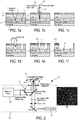
- Figure 2 illustrates the optical device 8.
- the optical device 8 comprises stage 33, a microscope 35, an objective 34 of the microscope 35, and a laser 17.
- Stage 33 is a piezoelectric stage 33 located in front of the objective 34.
- the process embodiment according to the invention then comprises the steps of:
- the sample 2 is imaged by fluorescence microscopy (using a microscope lamp 15 of microscope 35) and the emitters 1 are observed on the camera 16 of microscope 35 in an area of about 90 x 60 ⁇ m 2 .
- An area with an appropriate density of emitters 1 is chosen, and at the edges of this area, alignments marks comprising three 2D lattices 18 of holes 21 are burnt with the laser 17 focused by the microscope objective 34 (optical lithography).
- each hole 21 of the lattices 18 was burned by exposing the sample 2 to the focused beam of laser 17 (4.5 to 5 mW, continuous wave, 405 nm laser) for 3 seconds.
- the size of the imaged area depends on the field of view of the CCD camera 16 and the imaging optics.
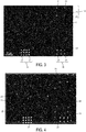
- Figure 3 is a fluorescence image of the emitters 1 and the lattices of the burnt holes 21.
- the sample 2 is imaged with a 100x objective 34.
- the 1392x1040 pixels on the image of CCD camera 16 corresponded to a real size of 92.17x68.86 ⁇ m 2 . From this is deduced the length of 1 pixel on the CCD camera image as 66.21 nm.
- the process embodiment according to the invention then comprises the step of imaging or determining, in a referential of the optical device 8, a position of each structure 1 and positions of markers 21 integral with the sample 2.
- Imaging or determining the position of each structure 1 in the referential of the optical device 8 comprises a step of acquiring an image imaging the markers 21 and a fluorescence radiation 14 from each structure 1.
- One corner hole 21 from each lattice 18 serves as an alignment marker for a upcoming electron beam lithography.
- the number of holes 21 in each lattice 18 is different, which makes them distinguishable: this allows designating a position to each fluorescing emitter 1 in the CCD (charged coupled device) camera image and helps in orienting the sample 2 throughout the protocol.
- the process embodiment according to the invention then comprises (before the steps of exposing to an electron beam the upper layer 4 of resist and removing all the thickness of the upper layer 4 of resist above the position of each selected structure 1), a step of selecting at least one selected structure 1 to be exposed to the e-beam lithography, this selection being based on detected light 14 emitted by the selected structure 1.
- the step of selecting the at least one selected structure 1 is based:
- an electron beam exposure pattern is created using a compatible software.
- the image dimensions are calibrated and its center is treated as the origin.
- the nanocrystals 1 to be exposed are assigned the coordinates accordingly.
- the shape to be exposed region is drawn.
- Figure 4 shows the electron beam writing exposure pattern drawn on the fluorescence image.
- the process embodiment according to the invention then comprises the step of putting the sample 2 in an electron-beam microscopy device (not illustrated).
- the process embodiment according to the invention comprises the step of, thanks to the electron-beam device, imaging or determining the position of each marker 21 in a referential of the electron-beam device.
- the sample 2 is scanned rapidly with scanning electron microscopy and the alignment lattices 18 are observed.
- the scanning should be quick and very optimized because a slow scan or multiple scans on the same area, especially at a high voltage, can expose the scanned PMMA and render the area useless for lithography.
- the marker positioning is confirmed, thus making the scanning electron microscopy output correspond with the fluorescence image via the electron beam lithography software.
- the electron beam is cut temporarily.
- the process embodiment according to the invention thus comprises, thanks to:
- the process embodiment according to the invention then comprises the step of, thanks to the electron-beam device, exposing to an electron beam the upper layer 4 of resist above the position of each selected structure 1.
- the upper resist 4 of thickness t RU is an electron resist.
- the lower resist 3 of thickness t RL protects the structure 1 of concern from destruction due to electrons.
- the amount of electron dose is chosen to be at least that is required to expose the upper resist 4.
- the thickness and type of the lower resist 3 is chosen to be such that the structure on which the electron-beam lithography is being performed is not completely destroyed by the electrons of the electron beam.
- the process embodiment according to the invention then comprises the step of, thanks to a solvent or a chemical solution, removing all the part of the at least two layers of resist 3, 4 previously submitted to the electron beam, i.e. a step of removing all the thickness of the upper layer 4 of resist above the position of each selected structure 1 but no part or only a non-complete part of the thickness of the lower layer 3 of resist above the position of each selected structure 1: after the electron beam exposure, the sample 2 is taken out of the electron-beam microscopy device, and immersed inversely and shaken in a bath of MIBK (methyl isobutyl ketone) and isopropanol (mixed in a ratio of 1:3) for 45s at 20 to 21°C.
- MIBK methyl isobutyl ketone
- the process embodiment according to the invention then comprises the step of, thanks to another solvent or chemical solution different from the previous solvent or chemical solution, removing part or all the remaining thickness of the lower layer 3 of resist above the position of each selected structure 1.
- Layer 3 (LOR®5A) beneath the etched holes 22, 23, 24 in PMMA is removed by immersing the sample 2 (inverted) in a bath of Microposit® MF®319 (a commercial developer manufactured by Shipley Co.) for 3 to 5s. This removes layer 3 (LOR®5A) from beneath the etched layer 4 (PMMA) and creates above each selected emitter 1 a hole 10 in layer 3 and an undercut 12 in the layer 4 (PMMA) as shown in step of Figure 1(d) .
- the image of Figure 6 is a fluorescence microscopy image of the working area after the development of layer 3 (LOR®5A).
- Material of layer 3 (LOR®5A) is a luminescent material. Therefore, its removal from some regions makes them appear darker in the image.
- Figure 6 shows several selected emitters 1 (white spots) inside developed holes 22, 23, 24.
- the process embodiment according to the invention then comprises the step of deposing a metallic layer 11 (or "patch" 11) in contact with the sample 2 and above the position of each selected structure 1, where all the thickness of the first 3 layer of resist and of the second 4 layer of resist have been removed.
- the plasmonic metal patch 11 and film 111 is deposited by physical vapor deposition.
- sample 2 is then immersed inverted and shaken in a bath of MF®319 for about 50s to perform the liftoff.
- This procedure removes layer 3 (LOR®5A), layer 4 (PMMA) and plasmonic metal film 111 from the vicinity of the plasmonic metal patch 11 located above each selected emitter 1, thus resulting in a plasmonic metal patch antenna.
- Figure 7 illustrates the measurement of the lifetime of a selected structure 1 (CdSe/CdS quantum dot) before the electron-beam lithography (line 19) and after the electron-beam lithography (line 20). In both the cases, the lifetime was noted to be 11 ns, which shows that the invention, due to its electron exposure prevention strategy, does not damage or change the emitter 1. Lifetime estimation is done by time resolved fluorescence measurement.
- the process according to the invention includes electron-beam lithography
- the emitters 1 above which the lithography is carried out are protected from direct and destructive electron exposure. Therefore, this technique can be used even on emitters 1 that are damaged by direct electron exposure.
- electron-beam lithography can be used to deterministically fabricate single emitter structures without exposing the emitter 1 directly and destructively to the electrons of the writing beam, and this is possible because the imaging of emitters 1 is not done using the conventional methods of scanning electron microscopy (which involves direct interaction of electrons with the emitters, both scanning electron microscopy and electron-beam lithography being carried out in the same machine) but with optical excitation and detection.
- the optical fluorescent image is used as an electron-beam writing pattern and the selected areas are exposed to pre-configured electron doses, which expose the resist 4 without damaging the emitters 1 beneath as they are protected by the lower thick layer 3 of the resist.
- the process according to the invention achieve the objective of realizing plasmonic (or photonic) nanostructures in which nanoemitters 1 are deterministically placed exactly at the position for which the resonant electromagnetic field is maximum, and thus the interaction between the emitters 1 and the field is as well maximum.
- Deterministic positioning of emitters 1 inside nanostructures means that the specific selected nanoemitters 1 with desirable properties (like emission wavelength, lifetime, polarization, etc.) can be chosen and included inside the fabricated nanostructure with control over the lateral and vertical positioning of the nanoemitter.
- the lithographic size attainable by the invention is limited by the resolution of electron-beam lithography (which is has a higher resolution than photolithography).
- the invention can be used at room temperature or at ultra low temperatures.
- the invention allows selecting any emitter(s) 1 [fragile or robust, single or aggregates] from randomly distributed emitters 1 and perform lithography above them. Though in the figures 1(a) to 1(f) the emitters 1 seem to aligned, but these emitters can be randomly oriented as well.
- the invention works at room temperature.
- the invention works also at low temperature.
- the invention is not limited to the fabrication of the antenna of figure 1(f) .
- the invention can be used to fabricate a variety of photonic structures that use single or multiple fluorescent structures 1 like quantum dots, nitrogen vacancy centers in nanodiamonds, etc.
- Examples of such photonic structures are single structure plasmonic patch antennas, metallo-dielectric antennas, Tamm structures, etc.
- the precision of the technique can be mainly improved by better calibration of distances on the fluorescence microscopy image (by using more appropriate optics, sub-pixel resolution) and more precise electron microscopy scanning of optical markers.
Landscapes
- Physics & Mathematics (AREA)
- General Physics & Mathematics (AREA)
- Chemical & Material Sciences (AREA)
- Analytical Chemistry (AREA)
- Engineering & Computer Science (AREA)
- Health & Medical Sciences (AREA)
- Nanotechnology (AREA)
- Pathology (AREA)
- General Health & Medical Sciences (AREA)
- Immunology (AREA)
- Biochemistry (AREA)
- Life Sciences & Earth Sciences (AREA)
- Nuclear Medicine, Radiotherapy & Molecular Imaging (AREA)
- Optics & Photonics (AREA)
- Condensed Matter Physics & Semiconductors (AREA)
- Manufacturing & Machinery (AREA)
- Crystallography & Structural Chemistry (AREA)
- Investigating, Analyzing Materials By Fluorescence Or Luminescence (AREA)
- Exposure And Positioning Against Photoresist Photosensitive Materials (AREA)
- Electron Beam Exposure (AREA)
Priority Applications (7)
| Application Number | Priority Date | Filing Date | Title |
|---|---|---|---|
| EP17305169.9A EP3364248A1 (de) | 2017-02-15 | 2017-02-15 | Elektronenstrahllithografieverfahren für eine probe mit mindestens einer zerbrechlichen nanostruktur |
| CN201880011977.XA CN110546571B (zh) | 2017-02-15 | 2018-02-12 | 适用于包含至少一个脆弱纳米结构体的样品的电子束光刻过程 |
| CA3048774A CA3048774C (en) | 2017-02-15 | 2018-02-12 | Electron-beam lithography process adapted for a sample comprising at least one fragile nanostructure |
| EP18707637.7A EP3583468B1 (de) | 2017-02-15 | 2018-02-12 | Elektronenstrahllithografieverfahren für eine probe mit mindestens einer zerbrechlichen nanostruktur |
| US16/486,061 US11127565B2 (en) | 2017-02-15 | 2018-02-12 | Electron-beam lithography process adapted for a sample comprising at least one fragile nanostructure |
| PCT/EP2018/053398 WO2018149777A1 (en) | 2017-02-15 | 2018-02-12 | Electron-beam lithography process adapted for a sample comprising at least one fragile nanostructure |
| JP2019545285A JP7050079B2 (ja) | 2017-02-15 | 2018-02-12 | 少なくとも1つの脆弱なナノ構造を含むサンプルに適した電子ビームリソグラフィプロセス |
Applications Claiming Priority (1)
| Application Number | Priority Date | Filing Date | Title |
|---|---|---|---|
| EP17305169.9A EP3364248A1 (de) | 2017-02-15 | 2017-02-15 | Elektronenstrahllithografieverfahren für eine probe mit mindestens einer zerbrechlichen nanostruktur |
Publications (1)
| Publication Number | Publication Date |
|---|---|
| EP3364248A1 true EP3364248A1 (de) | 2018-08-22 |
Family
ID=58709895
Family Applications (2)
| Application Number | Title | Priority Date | Filing Date |
|---|---|---|---|
| EP17305169.9A Withdrawn EP3364248A1 (de) | 2017-02-15 | 2017-02-15 | Elektronenstrahllithografieverfahren für eine probe mit mindestens einer zerbrechlichen nanostruktur |
| EP18707637.7A Active EP3583468B1 (de) | 2017-02-15 | 2018-02-12 | Elektronenstrahllithografieverfahren für eine probe mit mindestens einer zerbrechlichen nanostruktur |
Family Applications After (1)
| Application Number | Title | Priority Date | Filing Date |
|---|---|---|---|
| EP18707637.7A Active EP3583468B1 (de) | 2017-02-15 | 2018-02-12 | Elektronenstrahllithografieverfahren für eine probe mit mindestens einer zerbrechlichen nanostruktur |
Country Status (5)
| Country | Link |
|---|---|
| US (1) | US11127565B2 (de) |
| EP (2) | EP3364248A1 (de) |
| JP (1) | JP7050079B2 (de) |
| CN (1) | CN110546571B (de) |
| WO (1) | WO2018149777A1 (de) |
Families Citing this family (2)
| Publication number | Priority date | Publication date | Assignee | Title |
|---|---|---|---|---|
| US11791328B2 (en) * | 2021-12-20 | 2023-10-17 | Nanya Technology Corporation | Method for fabricating semiconductor device with integrated decoupling and alignment features |
| US20240234206A1 (en) * | 2022-08-19 | 2024-07-11 | California Institute Of Technology | Insulating self-developing resist for electronic devices and quantum point contacts |
Citations (8)
| Publication number | Priority date | Publication date | Assignee | Title |
|---|---|---|---|---|
| US20060098188A1 (en) * | 2004-11-09 | 2006-05-11 | Fei Company | Method of localizing fluorescent markers |
| US20080157404A1 (en) * | 2007-01-02 | 2008-07-03 | David Michael Fried | Trench structure and method for co-alignment of mixed optical and electron beam lithographic fabrication levels |
| US20130200262A1 (en) * | 2010-07-14 | 2013-08-08 | Delmic B.V. | Inspection apparatus and replaceable door for a vacuum chamber of such an inspection apparatus and a method for operating an inspection apparatus |
| US20130270596A1 (en) * | 2010-09-30 | 2013-10-17 | Universite Claude Bernard-Lyon 1 | Light sensors and sources comprising at least one microcavity with a localized tamm plasmon mode |
| EP2738607A1 (de) * | 2011-07-26 | 2014-06-04 | Institute Of Physics Chinese Academy Of Sciences | Nanographisches und ultrabreitbandige elektromagnetisches kennzeichenmesssystem |
| US20140302442A1 (en) * | 2013-04-04 | 2014-10-09 | Andreas Schell | Methods and fabrication tools for fabricating optical devices |
| CN104678716A (zh) * | 2015-02-09 | 2015-06-03 | 中国科学院半导体研究所 | 一种结合单量子点定位功能的激光直写光刻系统及其方法 |
| WO2016013930A1 (en) * | 2014-07-25 | 2016-01-28 | Delmic B.V. | Method for inspecting a sample using an assembly comprising a scanning electron microscope and a light microscope |
Family Cites Families (7)
| Publication number | Priority date | Publication date | Assignee | Title |
|---|---|---|---|---|
| JPS51147264A (en) * | 1975-06-13 | 1976-12-17 | Fujitsu Ltd | High-precision positioning system |
| US7160654B2 (en) * | 2003-12-02 | 2007-01-09 | Taiwan Semiconductor Manufacturing Co., Ltd. | Method of the adjustable matching map system in lithography |
| JP2005175166A (ja) | 2003-12-10 | 2005-06-30 | Sony Corp | 露光方法および露光システム |
| US7696057B2 (en) * | 2007-01-02 | 2010-04-13 | International Business Machines Corporation | Method for co-alignment of mixed optical and electron beam lithographic fabrication levels |
| NL2004531A (nl) * | 2009-05-29 | 2010-11-30 | Asml Netherlands Bv | Apparatus and method for providing resist alignment marks in a double patterning lithographic process. |
| EP3175495B1 (de) | 2014-08-01 | 2020-01-01 | Orthogonal Inc. | Potolithografische strukturierung von vorrichtungen |
| EP3364249A1 (de) * | 2017-02-15 | 2018-08-22 | Centre National De La Recherche Scientifique | Adaptiertes optisches lithografieverfahren für eine probe mit mindestens einem zerbrechlichen lichtemitter |
-
2017
- 2017-02-15 EP EP17305169.9A patent/EP3364248A1/de not_active Withdrawn
-
2018
- 2018-02-12 JP JP2019545285A patent/JP7050079B2/ja active Active
- 2018-02-12 US US16/486,061 patent/US11127565B2/en active Active
- 2018-02-12 EP EP18707637.7A patent/EP3583468B1/de active Active
- 2018-02-12 CN CN201880011977.XA patent/CN110546571B/zh active Active
- 2018-02-12 WO PCT/EP2018/053398 patent/WO2018149777A1/en not_active Ceased
Patent Citations (8)
| Publication number | Priority date | Publication date | Assignee | Title |
|---|---|---|---|---|
| US20060098188A1 (en) * | 2004-11-09 | 2006-05-11 | Fei Company | Method of localizing fluorescent markers |
| US20080157404A1 (en) * | 2007-01-02 | 2008-07-03 | David Michael Fried | Trench structure and method for co-alignment of mixed optical and electron beam lithographic fabrication levels |
| US20130200262A1 (en) * | 2010-07-14 | 2013-08-08 | Delmic B.V. | Inspection apparatus and replaceable door for a vacuum chamber of such an inspection apparatus and a method for operating an inspection apparatus |
| US20130270596A1 (en) * | 2010-09-30 | 2013-10-17 | Universite Claude Bernard-Lyon 1 | Light sensors and sources comprising at least one microcavity with a localized tamm plasmon mode |
| EP2738607A1 (de) * | 2011-07-26 | 2014-06-04 | Institute Of Physics Chinese Academy Of Sciences | Nanographisches und ultrabreitbandige elektromagnetisches kennzeichenmesssystem |
| US20140302442A1 (en) * | 2013-04-04 | 2014-10-09 | Andreas Schell | Methods and fabrication tools for fabricating optical devices |
| WO2016013930A1 (en) * | 2014-07-25 | 2016-01-28 | Delmic B.V. | Method for inspecting a sample using an assembly comprising a scanning electron microscope and a light microscope |
| CN104678716A (zh) * | 2015-02-09 | 2015-06-03 | 中国科学院半导体研究所 | 一种结合单量子点定位功能的激光直写光刻系统及其方法 |
Non-Patent Citations (1)
| Title |
|---|
| DATABASE EPODOC EUROPEAN PATENT OFFICE, THE HAGUE, NL; 3 June 2015 (2015-06-03), "Laser direct writing photolithographic system combined with single quantum dot locating function and method thereof", XP002772422 * |
Also Published As
| Publication number | Publication date |
|---|---|
| CA3048774A1 (en) | 2018-08-23 |
| EP3583468A1 (de) | 2019-12-25 |
| CN110546571B (zh) | 2021-10-22 |
| US11127565B2 (en) | 2021-09-21 |
| CN110546571A (zh) | 2019-12-06 |
| JP2020508578A (ja) | 2020-03-19 |
| EP3583468B1 (de) | 2021-04-07 |
| WO2018149777A1 (en) | 2018-08-23 |
| JP7050079B2 (ja) | 2022-04-07 |
| US20200006037A1 (en) | 2020-01-02 |
Similar Documents
| Publication | Publication Date | Title |
|---|---|---|
| Liu et al. | Nanoscale positioning approaches for integrating single solid‐state quantum emitters with photonic nanostructures | |
| US7476787B2 (en) | Addressable field enhancement microscopy | |
| US20180080885A1 (en) | Cathodoluminescence-activated nanoscale imaging | |
| EP3583468B1 (de) | Elektronenstrahllithografieverfahren für eine probe mit mindestens einer zerbrechlichen nanostruktur | |
| Fleischer et al. | Tailoring gold nanostructures for near-field optical applications | |
| CA3048774C (en) | Electron-beam lithography process adapted for a sample comprising at least one fragile nanostructure | |
| EP3583469B1 (de) | Adaptiertes optisches lithografieverfahren für eine probe mit mindestens einem zerbrechlichen lichtemitter | |
| Humbert et al. | Large-scale controlled coupling of single-photon emitters to high-index dielectric nanoantennas by AFM nanoxerography | |
| US7351374B2 (en) | Surface plasmon enhanced illumination apparatus having non-periodic resonance configurations | |
| JP4887494B2 (ja) | 蛍光目盛り基盤、蛍光目盛り付き顕微鏡基盤及び蛍光目盛り付き顕微鏡用試料容器 | |
| US12476436B2 (en) | Systems and methods for microdisk and multiplet laser particles | |
| JP2020508578A5 (de) | ||
| US20110186756A1 (en) | Method of fabricating a single photon source | |
| Liu et al. | Nanoscale positioning approaches for integrating single epitaxial quantum emitters with photonic nanostructures | |
| JP2004117267A (ja) | 蛍光顕微鏡用解像度評価チャート、およびその製造方法 | |
| Meldrum et al. | Two-dimensionally-patterned silicon nanocrystal arrays | |
| RU204747U1 (ru) | Источник одиночных фотонов на основе двумерного полупроводника с излучением в нанофотонный волновод | |
| Stomeo et al. | Rapid prototyping of two-dimensional photonic crystal devices by a dual beam focused ion beam system | |
| Wai | Elucidating dynamics in soft materials using low-dose electron and cathodoluminescence microscopy | |
| Bollani et al. | Photoluminescence emission from a nanofabricated scanning probe tip made of epitaxial germanium | |
| Peter et al. | Fabrication and characterization of active plasmonic antennas | |
| WO2007011876A1 (en) | Surface plasmon enhanced illumination apparatus having non-periodic resonance configurations | |
| Poujet et al. | Enhanced transmission of light through coaxial nano-structures in a silver film: theory and first experimental results | |
| Jiang et al. | Cavity-Free, Matrix-Addressable Quantum Dot Architecture for On-Chip Optical Switching | |
| JP2001296231A (ja) | 近接場光学装置評価用試料およびその作成法 |
Legal Events
| Date | Code | Title | Description |
|---|---|---|---|
| PUAI | Public reference made under article 153(3) epc to a published international application that has entered the european phase |
Free format text: ORIGINAL CODE: 0009012 |
|
| STAA | Information on the status of an ep patent application or granted ep patent |
Free format text: STATUS: THE APPLICATION HAS BEEN PUBLISHED |
|
| AK | Designated contracting states |
Kind code of ref document: A1 Designated state(s): AL AT BE BG CH CY CZ DE DK EE ES FI FR GB GR HR HU IE IS IT LI LT LU LV MC MK MT NL NO PL PT RO RS SE SI SK SM TR |
|
| AX | Request for extension of the european patent |
Extension state: BA ME |
|
| STAA | Information on the status of an ep patent application or granted ep patent |
Free format text: STATUS: REQUEST FOR EXAMINATION WAS MADE |
|
| 17P | Request for examination filed |
Effective date: 20190122 |
|
| RBV | Designated contracting states (corrected) |
Designated state(s): AL AT BE BG CH CY CZ DE DK EE ES FI FR GB GR HR HU IE IS IT LI LT LU LV MC MK MT NL NO PL PT RO RS SE SI SK SM TR |
|
| GRAP | Despatch of communication of intention to grant a patent |
Free format text: ORIGINAL CODE: EPIDOSNIGR1 |
|
| STAA | Information on the status of an ep patent application or granted ep patent |
Free format text: STATUS: GRANT OF PATENT IS INTENDED |
|
| INTG | Intention to grant announced |
Effective date: 20190409 |
|
| RIN1 | Information on inventor provided before grant (corrected) |
Inventor name: SENELLART, PASCALE Inventor name: BELACEL, CHERIF Inventor name: DHAWAN, AMIT RAJ Inventor name: MAITRE, AGNES |
|
| STAA | Information on the status of an ep patent application or granted ep patent |
Free format text: STATUS: THE APPLICATION IS DEEMED TO BE WITHDRAWN |
|
| 18D | Application deemed to be withdrawn |
Effective date: 20190820 |