EP3364249A1 - Adaptiertes optisches lithografieverfahren für eine probe mit mindestens einem zerbrechlichen lichtemitter - Google Patents
Adaptiertes optisches lithografieverfahren für eine probe mit mindestens einem zerbrechlichen lichtemitter Download PDFInfo
- Publication number
- EP3364249A1 EP3364249A1 EP17305170.7A EP17305170A EP3364249A1 EP 3364249 A1 EP3364249 A1 EP 3364249A1 EP 17305170 A EP17305170 A EP 17305170A EP 3364249 A1 EP3364249 A1 EP 3364249A1
- Authority
- EP
- European Patent Office
- Prior art keywords
- emitter
- layer
- light beam
- process according
- resist
- Prior art date
- Legal status (The legal status is an assumption and is not a legal conclusion. Google has not performed a legal analysis and makes no representation as to the accuracy of the status listed.)
- Withdrawn
Links
Images


Classifications
-
- G—PHYSICS
- G03—PHOTOGRAPHY; CINEMATOGRAPHY; ANALOGOUS TECHNIQUES USING WAVES OTHER THAN OPTICAL WAVES; ELECTROGRAPHY; HOLOGRAPHY
- G03F—PHOTOMECHANICAL PRODUCTION OF TEXTURED OR PATTERNED SURFACES, e.g. FOR PRINTING, FOR PROCESSING OF SEMICONDUCTOR DEVICES; MATERIALS THEREFOR; ORIGINALS THEREFOR; APPARATUS SPECIALLY ADAPTED THEREFOR
- G03F7/00—Photomechanical, e.g. photolithographic, production of textured or patterned surfaces, e.g. printing surfaces; Materials therefor, e.g. comprising photoresists; Apparatus specially adapted therefor
- G03F7/70—Microphotolithographic exposure; Apparatus therefor
- G03F7/70216—Mask projection systems
- G03F7/70283—Mask effects on the imaging process
- G03F7/70291—Addressable masks, e.g. spatial light modulators [SLMs], digital micro-mirror devices [DMDs] or liquid crystal display [LCD] patterning devices
-
- G—PHYSICS
- G03—PHOTOGRAPHY; CINEMATOGRAPHY; ANALOGOUS TECHNIQUES USING WAVES OTHER THAN OPTICAL WAVES; ELECTROGRAPHY; HOLOGRAPHY
- G03F—PHOTOMECHANICAL PRODUCTION OF TEXTURED OR PATTERNED SURFACES, e.g. FOR PRINTING, FOR PROCESSING OF SEMICONDUCTOR DEVICES; MATERIALS THEREFOR; ORIGINALS THEREFOR; APPARATUS SPECIALLY ADAPTED THEREFOR
- G03F7/00—Photomechanical, e.g. photolithographic, production of textured or patterned surfaces, e.g. printing surfaces; Materials therefor, e.g. comprising photoresists; Apparatus specially adapted therefor
- G03F7/70—Microphotolithographic exposure; Apparatus therefor
- G03F7/70058—Mask illumination systems
- G03F7/70133—Measurement of illumination distribution, in pupil plane or field plane
-
- B—PERFORMING OPERATIONS; TRANSPORTING
- B82—NANOTECHNOLOGY
- B82Y—SPECIFIC USES OR APPLICATIONS OF NANOSTRUCTURES; MEASUREMENT OR ANALYSIS OF NANOSTRUCTURES; MANUFACTURE OR TREATMENT OF NANOSTRUCTURES
- B82Y30/00—Nanotechnology for materials or surface science, e.g. nanocomposites
-
- G—PHYSICS
- G02—OPTICS
- G02B—OPTICAL ELEMENTS, SYSTEMS OR APPARATUS
- G02B21/00—Microscopes
- G02B21/0004—Microscopes specially adapted for specific applications
- G02B21/002—Scanning microscopes
-
- G—PHYSICS
- G02—OPTICS
- G02B—OPTICAL ELEMENTS, SYSTEMS OR APPARATUS
- G02B21/00—Microscopes
- G02B21/06—Means for illuminating specimens
-
- G—PHYSICS
- G02—OPTICS
- G02B—OPTICAL ELEMENTS, SYSTEMS OR APPARATUS
- G02B27/00—Optical systems or apparatus not provided for by any of the groups G02B1/00 - G02B26/00, G02B30/00
- G02B27/09—Beam shaping, e.g. changing the cross-sectional area, not otherwise provided for
- G02B27/0938—Using specific optical elements
- G02B27/095—Refractive optical elements
-
- G—PHYSICS
- G03—PHOTOGRAPHY; CINEMATOGRAPHY; ANALOGOUS TECHNIQUES USING WAVES OTHER THAN OPTICAL WAVES; ELECTROGRAPHY; HOLOGRAPHY
- G03F—PHOTOMECHANICAL PRODUCTION OF TEXTURED OR PATTERNED SURFACES, e.g. FOR PRINTING, FOR PROCESSING OF SEMICONDUCTOR DEVICES; MATERIALS THEREFOR; ORIGINALS THEREFOR; APPARATUS SPECIALLY ADAPTED THEREFOR
- G03F7/00—Photomechanical, e.g. photolithographic, production of textured or patterned surfaces, e.g. printing surfaces; Materials therefor, e.g. comprising photoresists; Apparatus specially adapted therefor
- G03F7/70—Microphotolithographic exposure; Apparatus therefor
- G03F7/70383—Direct write, i.e. pattern is written directly without the use of a mask by one or multiple beams
- G03F7/70391—Addressable array sources specially adapted to produce patterns, e.g. addressable LED arrays
-
- G—PHYSICS
- G03—PHOTOGRAPHY; CINEMATOGRAPHY; ANALOGOUS TECHNIQUES USING WAVES OTHER THAN OPTICAL WAVES; ELECTROGRAPHY; HOLOGRAPHY
- G03F—PHOTOMECHANICAL PRODUCTION OF TEXTURED OR PATTERNED SURFACES, e.g. FOR PRINTING, FOR PROCESSING OF SEMICONDUCTOR DEVICES; MATERIALS THEREFOR; ORIGINALS THEREFOR; APPARATUS SPECIALLY ADAPTED THEREFOR
- G03F9/00—Registration or positioning of originals, masks, frames, photographic sheets or textured or patterned surfaces, e.g. automatically
- G03F9/70—Registration or positioning of originals, masks, frames, photographic sheets or textured or patterned surfaces, e.g. automatically for microlithography
- G03F9/7003—Alignment type or strategy, e.g. leveling, global alignment
- G03F9/7007—Alignment other than original with workpiece
- G03F9/7015—Reference, i.e. alignment of original or workpiece with respect to a reference not on the original or workpiece
-
- G—PHYSICS
- G03—PHOTOGRAPHY; CINEMATOGRAPHY; ANALOGOUS TECHNIQUES USING WAVES OTHER THAN OPTICAL WAVES; ELECTROGRAPHY; HOLOGRAPHY
- G03F—PHOTOMECHANICAL PRODUCTION OF TEXTURED OR PATTERNED SURFACES, e.g. FOR PRINTING, FOR PROCESSING OF SEMICONDUCTOR DEVICES; MATERIALS THEREFOR; ORIGINALS THEREFOR; APPARATUS SPECIALLY ADAPTED THEREFOR
- G03F9/00—Registration or positioning of originals, masks, frames, photographic sheets or textured or patterned surfaces, e.g. automatically
- G03F9/70—Registration or positioning of originals, masks, frames, photographic sheets or textured or patterned surfaces, e.g. automatically for microlithography
- G03F9/7073—Alignment marks and their environment
- G03F9/7084—Position of mark on substrate, i.e. position in (x, y, z) of mark, e.g. buried or resist covered mark, mark on rearside, at the substrate edge, in the circuit area, latent image mark, marks in plural levels
-
- G—PHYSICS
- G01—MEASURING; TESTING
- G01N—INVESTIGATING OR ANALYSING MATERIALS BY DETERMINING THEIR CHEMICAL OR PHYSICAL PROPERTIES
- G01N21/00—Investigating or analysing materials by the use of optical means, i.e. using sub-millimetre waves, infrared, visible or ultraviolet light
- G01N21/62—Systems in which the material investigated is excited whereby it emits light or causes a change in wavelength of the incident light
- G01N21/63—Systems in which the material investigated is excited whereby it emits light or causes a change in wavelength of the incident light optically excited
- G01N21/64—Fluorescence; Phosphorescence
- G01N21/6408—Fluorescence; Phosphorescence with measurement of decay time, time resolved fluorescence
-
- G—PHYSICS
- G01—MEASURING; TESTING
- G01N—INVESTIGATING OR ANALYSING MATERIALS BY DETERMINING THEIR CHEMICAL OR PHYSICAL PROPERTIES
- G01N21/00—Investigating or analysing materials by the use of optical means, i.e. using sub-millimetre waves, infrared, visible or ultraviolet light
- G01N21/62—Systems in which the material investigated is excited whereby it emits light or causes a change in wavelength of the incident light
- G01N21/63—Systems in which the material investigated is excited whereby it emits light or causes a change in wavelength of the incident light optically excited
- G01N21/64—Fluorescence; Phosphorescence
- G01N21/6445—Measuring fluorescence polarisation
-
- G—PHYSICS
- G01—MEASURING; TESTING
- G01N—INVESTIGATING OR ANALYSING MATERIALS BY DETERMINING THEIR CHEMICAL OR PHYSICAL PROPERTIES
- G01N21/00—Investigating or analysing materials by the use of optical means, i.e. using sub-millimetre waves, infrared, visible or ultraviolet light
- G01N21/62—Systems in which the material investigated is excited whereby it emits light or causes a change in wavelength of the incident light
- G01N21/63—Systems in which the material investigated is excited whereby it emits light or causes a change in wavelength of the incident light optically excited
- G01N21/64—Fluorescence; Phosphorescence
- G01N21/645—Specially adapted constructive features of fluorimeters
- G01N21/6456—Spatial resolved fluorescence measurements; Imaging
- G01N21/6458—Fluorescence microscopy
-
- G—PHYSICS
- G01—MEASURING; TESTING
- G01N—INVESTIGATING OR ANALYSING MATERIALS BY DETERMINING THEIR CHEMICAL OR PHYSICAL PROPERTIES
- G01N21/00—Investigating or analysing materials by the use of optical means, i.e. using sub-millimetre waves, infrared, visible or ultraviolet light
- G01N21/62—Systems in which the material investigated is excited whereby it emits light or causes a change in wavelength of the incident light
- G01N21/63—Systems in which the material investigated is excited whereby it emits light or causes a change in wavelength of the incident light optically excited
- G01N21/64—Fluorescence; Phosphorescence
- G01N21/6489—Photoluminescence of semiconductors
-
- H—ELECTRICITY
- H10—SEMICONDUCTOR DEVICES; ELECTRIC SOLID-STATE DEVICES NOT OTHERWISE PROVIDED FOR
- H10H—INORGANIC LIGHT-EMITTING SEMICONDUCTOR DEVICES HAVING POTENTIAL BARRIERS
- H10H20/00—Individual inorganic light-emitting semiconductor devices having potential barriers, e.g. light-emitting diodes [LED]
- H10H20/80—Constructional details
- H10H20/81—Bodies
- H10H20/811—Bodies having quantum effect structures or superlattices, e.g. tunnel junctions
- H10H20/812—Bodies having quantum effect structures or superlattices, e.g. tunnel junctions within the light-emitting regions, e.g. having quantum confinement structures
Definitions
- the present invention relates to a lithography process.
- Photonic and plasmonic nanostructures within which individual (or aggregates) fluorescent nanoemitters like quantum dots, nitrogen vacancy centers in nanodiamonds, and fluorescent molecules are placed with nanometric precision find applications in many fields like single photon emission and plasmonics, and these structures serve as an ideal tool for investigating light-matter interactions at a single emitter level.
- the fabrication of such structures requires nanometric lateral and vertical control over placing the nanoemitter inside the structure. For this purpose, lithography has to be performed around nanoemitters, without destroying them. This task becomes very difficult when dealing with individual nanoemitters because an individual emitter is not as robust and bright as an aggregate of emitters.
- An object of this invention is to propose a lithography process that can be performed on fragile emitters (in particular individual or single emitters) with limited risks to photobleach or destroy the emitters compared to prior art.
- An aspect of the invention concerns a lithography process on a sample comprising at least one emitter, said process comprising:
- the intermediate part can be surrounding the selected emitter, and/or the shaped light beam can be centered on the position of the selected emitter.
- the central part can be:
- the light for exciting the selected emitter can come from the same source than the shaped light beam.
- the light for exciting the selected emitter can be the shaped light beam, but not necessarily with the same light power.
- the light for exciting the selected emitter can have a power lower than the power of the shaped light beam used for curing a part of the at least one layer of resist by putting the light beam above the position of the selected emitter.
- the light for exciting the selected emitter can have a power at least 1000 times lower than the power of the shaped light beam used for curing a part of the at least one layer of resist by putting the light beam above the position of the selected emitter.
- the shaped light beam can be a spatially shaped laser mode.
- the shaped light beam can be:
- the intensity of the shaped light beam on the at least one layer of resist can reach a minimum at the central part.
- the process according to the invention can further comprise, before the curing step, a step of selecting the selected emitter based on the detected light emitted by the selected emitter.
- the step of selecting the selected emitter can be based:
- the curing step can create a surrounding burnt above the position of the selected emitter.
- the process according to the invention can comprise, after the curing step, removing the part of the at least one layer of resist located inside the surrounding burnt, the surrounding burnt then becoming a hole located inside the at least one layer of resist and above the position of the selected emitter.
- the process according to the invention can comprise a step of depositing a metallic layer inside the hole (preferably in contact with the sample), above the position of the selected emitter.
- the at least one layer of resist can comprise two layers of two different resists, the two layers comprising a first layer in contact with the sample and a second layer in contact with the first layer.
- the at least one emitter can be comprised in the sample inside an emitter layer.
- the at least one emitter can be comprised in the sample between two layers of the same dielectric material forming the emitter layer.
- One first side of the emitter layer can be in contact with the at least one layer of resist, and/or one second side of the emitter layer can be in contact with a metallic layer or a Bragg mirror.
- Each emitter can be a fluorescent emitter or a photoluminescent emitter.
- Each emitter can be a quantum dot, a nitrogen vacancy center in a nanodiamond, a fluorescent molecule, or a defect in a monolayer two dimensional material (like MoS 2 , WSe 2 ).
- variants of the invention including only a selection of characteristics subsequently described or illustrated, isolated from other described or illustrated characteristics (even if this selection is taken from a sentence containing these other characteristics), if this selection of characteristics is sufficient to give a technical advantage or to distinguish the invention over the state of the art.
- This selection includes at least one characteristic, preferably a functional characteristic without structural details, or with only a part of the structural details if that part is sufficient to give a technical advantage or to distinguish the invention over the state of the art.
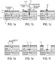
- This lithography process embodiment according to the invention is implemented on a sample 2 comprising at least one emitter 1.
- Each emitter is an individual emitter 1 (i.e. an emitter capable of emitting one single photon at a time) or an aggregate emitter 1 (formed by an assembly of a plurality of individual emitters 1).
- Each emitter 1 is preferably an individual emitter 1.
- Each emitter is a nano-emitter, i.e. an emitter having a volume that can completely enter inside a sphere having a 100nm diameter.
- Each emitter 1 is something that emits light after absorbing photons.
- the absorbed photons can be optical, ultraviolet, infrared, or in general, from any part of the electromagnetic spectrum.
- Each emitter 1 can be a fluorescent emitter or a photoluminescent emitter.
- Each emitter 1 is typically a quantum dot, a nitrogen vacancy center in a nanodiamond, a fluorescent molecule, or a defect in a monolayer two dimensional material like MoS 2 , WSe 2 .
- each emitter 1 is a CdSe/CdS quantum dot, more precisely a CdSe/CdS core/shell colloidal quantum dot.
- the at least one emitter 1 is comprised in the sample 2 inside an emitter layer 7a, 7b.
- the at least one emitter 1 is comprised in the sample between two layers 7a, 7b, preferably two layers 7a, 7b of the same dielectric material forming the emitter layer, typically PMMA (polymethyl methacrylate).
- PMMA polymethyl methacrylate
- the sample 2 comprises an intermediate layer 6 comprised between a substrate 5 (typically a silicon wafer) and the emitter layer 7a, 7b.
- the intermediate layer 6 is a metallic layer 6.
- gold (Au) was chosen as the plasmonic metal.
- the sample 2 is prepared as follow:
- the process embodiment according to the invention comprises the step of putting at least one layer 3, 4 of resist above the sample 2.
- the at least one layer 3, 4 of resist comprises two layers of two different resists, the two layers comprising a first layer 3 (LOR) in contact with the sample 2 and a second (or top) layer 4 (PMMA) above (preferably in contact with) the first layer 3.
- LOR first layer 3
- PMMA second (or top) layer 4
- LOR®5A is a commercial lithography liftoff resist manufactured by MicroChem Corp.
- a 50 nm thick layer 4 of PMMA (polymethyl methacrylate) is spincoated and baked.
- One first side of the emitter layer 7a, 7b is in contact with the at least one layer 3, 4 of resist.
- One second side of the emitter layer 7a, 7b is in contact with the metallic layer 6.
- Figure 3 illustrates a device or optical setup 8 for implementing some steps of the process embodiment according to the invention.
- Beam profiles which are circularly symmetric (or lasers with cavities that are cylindrically symmetric) are often best solved using the Laguerre-Gaussian modal decomposition LG l, p .
- These functions are written in cylindrical coordinates using Laguerre polynomials.
- Each transverse mode LG l, p is again labelled using two integers, in this case the radial index p ⁇ 0 and the azimuthal index I which can be positive or negative or zero.
- FIG 2a illustrates the part 21 of the optical setup 8 used to modulate the phase of an incident laser beam 30 and generate other modes, such as LG and Bessel beams.
- the incident laser beam 30 of a 473 nm continuous wave diode laser 19 is sent through a polarizing beam splitter (PBS) cube 22, which selects only the s-polarization part of the laser.
- PBS polarizing beam splitter
- a diode laser is generally polarized and by letting it pass through a PBS 22, we enhance the polarization purity of the transmitted laser light.
- the beam 30 is spatially filtered by a diaphragm 23 and transmitted through a half-wave plate 24 (or retarder).
- This halfwave plate 24 and a following PBS 25 allow us to control the power of the laser beam incident on a spatial light modulator (SLM) screen 26.
- SLM spatial light modulator
- the beam 30 After passing through another diaphragm 27, the beam 30 passes through an assembly of two lenses 28, 29, which acts as a beam expander.
- lenses 28, 29 of focal lengths f1 and f2, respectively we attain a beam expansion of f2/f1 (we use a 5x beam expander).
- the goal of beam expansion is to cover the entire screen of the SLM 26; it eases the alignment of the centers of the phase mask 26 and the incident laser beam 30 (which results in better modulation) and reduces the incident laser beam intensity on the SLM screen 26 (thus preventing damage to the liquid crystals).
- the expanded laser beam 30 passes through the PBS 25, through which only the s-polarization is transmitted.
- the transmitted light beam 30 is incident on the phase-only reflective SLM screen 26, which is connected to a computer and an LG l, p explicit phase mask (with an included binary blazed grating) is displayed on it.
- the direction of the optic axis of the SLM screen is almost parallel to the polarization of the incident beam.
- the resulting consists of the phase-modulated diffracted light (which includes several orders of the diffraction) and the zero-order or undiffracted light.
- the blazed grating separates the zero-order spot from the first order of the diffracted LG mode, and the diaphragm 43 spatially filters only the first order of diffraction.
- the selected first diffraction order 13, 15 can be propagated and aligned as required.
- the sample 2 is put on a motorized (piezoelectric) stage 33 in front of an objective 34 of a microscope 35.
- the process embodiment according to the invention then comprises exciting steps comprising exciting one after the other a plurality of emitters 1 including one selected emitter 1, with light 13 through the at least one layer of resist 3,4.
- This excitation light 13 is the previously described selected first diffraction order.
- Light 13 is also called excitation beam 13.
- Light 13 is a spatially shaped laser mode.
- the process embodiment according to the invention also comprises detecting steps comprising detecting one after the other the light 14 emitted each excited emitter 1 including the selected emitter 1, and determining a position of each excited emitter 1 including the selected emitter 1.
- the detected light 14 is fluorescence light.
- the detected light 14 is collected, detected and analyzed thanks to a Hanbury Brown and Twiss setup 36.
- the process embodiment according to the invention then comprises (before the following curing step), a step of selecting the selected emitter 1 among all the excited emitters 1, this selection being based on the detected light 14 emitted by the selected emitter 1.
- the step of selecting the selected emitter 1 is based:
- the exciting steps and detecting steps are part of a scanning step.
- Sample 2 is scanned by confocal microscopy and the selected emitter 1 is selected as previously explained.
- the selected emitter 1 is scanned using the previously described donut Laguerre-Gaussian mode (170 nW and 473 nm continuous wave laser).
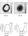
- Figure 3 shows the optical setup 8 and a confocal scan image 31 of the selected emitter 1 made using the LG l,p laser mode.
- the donut shape is not perfectly circular mainly due to the large angle of reflection of the SLM screen, and then the mirrors used for guiding the LG mode into the microscope are not exactly at 45° to the incident light.
- each imaged pixel of the scan image 31 corresponds to a specific relative position between the sample 2 and the excitation beam 13.
- the position of the selected emitter 1 is determined as being the relative position between the sample 2 and the beam 13, 15 obtained for imaging the pixel (in image 31) at the center of the donut or closed loop shape of beam 13, 15.
- the process embodiment according to the invention then comprises curing with a light beam 15 a part of the at least one layer 3, 4 of resist by putting the light beam 15 above the position of the selected emitter 1.
- Beam 15 is also called the curing beam 15.
- This light beam 15 is the previously described selected first diffraction order.
- the light beam 15 is shaped by the spatial light modulator 26.
- the light beam 15 is a shaped light beam 15, and a cross section of this light beam 15 (in a plane perpendicular to the optical axis of objective 34 or perpendicular to an average direction of propagation of this beam 15 onto the at least one layer 3, 4 and/or onto the selected emitter 1), imaged (and focused) on the emitter 1, has:
- the intensity of the curing shaped light beam 15 on the at least one layer 3, 4 of resist reaches a maximum (compared to the central part 16 and the border part 18) at the intermediate part 17, and is even maximum (compared to the central part 16 and the border part 18) over all the intermediate part 17.
- the intermediate part 17 is surrounding the selected emitter 1.
- the curing shaped light beam 15 is centered or substantially centered on the position of the selected emitter 1 (i.e. the central part 16 is right above the selected emitter 1).
- the curing shaped light beam 15 is a spatially shaped laser mode.
- the intensity of the curing shaped light beam 15 on the at least one layer 3, 4 of resist reach a minimum (compared to the intermediate part 17 and the border part 18) at the central part 16, this minimum intensity having a value at least one hundred times inferior to the value of the maximum intensity of the intermediate part 17.
- This minimum is preferably a zero intensity or a substantially zero intensity.
- the light 13 for exciting the selected emitter 1 comes from the same source 19 than the curing shaped light beam 15.
- the excitation beam 13 for exciting the selected emitter 1 is the same beam than the curing shaped light beam 15 (i.e. beams 13 and 15 have the same laser mode(s), the same shape, the same size(s)), except that preferably the excitation beam 13 and the curing light beam 15 do not have the same light power.
- the light 13 for exciting the selected emitter 1 has a power lower than the power of the shaped light beam 15 used for curing a part of the at least one layer 3, 4 of resist by putting the light beam 15 above the position of the selected emitter 1.
- the light 13 for exciting the selected emitter 1 has a power at least 1000 times (preferably at least 10000 times) lower than the power of the shaped light beam 15 used for curing a part of the at least one layer 3, 4 of resist by putting the light beam 15 above the position of the selected emitter 1.
- the selected emitter 1 is located with a low power laser 13 and the resist 3, 4 on top of it is burned with a high power laser 15.
- the 473 nm laser is blocked from entering into the microscope 35. After setting the power of the first order of the donut Laguerre- Gaussian mode to 7 mW, it is let into the microscope 35 for a duration of 90s. In this time resist bi-layer 3, 4 above the selected emitter 1 is burned.
- the invention circumvents the problem of emitter bleaching and performs optical lithography centered over a single or aggregates of fluorescent emitters 1 without causing any harm to the emitter 1. This is because the light intensity at the center of a donut laser mode is ideally zero, and during the lithography process embodiment according to the invention, the emitter 1 is placed at the center of the donut laser mode. The optical lithography is performed on the resist 3, 4 above the emitter 1.
- the lateral accuracy of positioning the emitter 1 inside the nanostructure is decided by the imaging optics ( ⁇ 50 nm easily possible), and the vertical accuracy depends on the deposition method ( ⁇ 3 nm can be achieved if spin-coating or physical vapor deposition techniques are used).
- the optical lithography process according to the invention can be carried out on an optical table, using widely available optical microscopes, lasers, and spatial light modulators.
- the curing step creates a surrounding burnt 20 above the position of the selected emitter 1.
- the surrounding burnt 20 from the front view of the sample 2 from the side of the at least one layer 3, 4 of resist, surrounds the selected emitter 1.
- the surrounding burnt can have a shape of ring, circle, ellipse, or any closed curve surrounding the selected emitter.
- the process embodiment according to the invention comprises, after the curing step, removing all the part of the at least one layer 3, 4 of resist located inside the surrounding burnt 20, the surrounding burnt 20 then becoming a hole 10 located inside the at least one layer 3, 4 of resist and above the position of the selected emitter 1.
- the sample 2 is immersed in a bath of Micorposit® MF®-319 solvent (this is a commercial developer made by Shipley Co.) for 3 to 5s. MF-319 solvent, without attacking PMMA, develops LOR. It develops LOR®5A and creates an undercut 12 in the PMMA layer 4 above it.
- Figure 4(b) is an atomic force microscopy image of the hole 10 corresponding to the step of figure 1(d) ; the corresponding height profile is given in Figure 4(d) ;
- the process embodiment according to the invention then comprises a step of depositing a metallic layer 11 (or "patch” 11) inside the hole 10, in contact with the sample 2 and above the position of the selected emitter 1.
- the plasmonic metal (gold) for the patch 11 and film 111 is deposited by physical vapor deposition.
- the typical thickness of patch 11 is comprised between 5 nm and 50 nm.
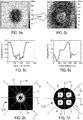
- Figure 5(b) is a zoom of figure 5(a) ; the corresponding height profile is given in Figure 5(d) .
- the invention allows selecting any emitter(s) 1 [fragile or robust, single or aggregates] from randomly distributed emitters 1 and perform lithography above them. Though in the figures 1(a) to 1(f) the emitters 1 seem to aligned, but these emitters can be randomly oriented as well.
- the invention works at room temperature.
- the invention works also at low temperature.
- the invention is not limited to the fabrication of the antenna of figure 1(f) .
- the invention can be used to fabricate a variety of photonic structures that use single or multiple fluorescent emitters 1 like quantum dots, nitrogen vacancy centers in nanodiamonds, etc.
- photonic structures are single emitter plasmonic patch antennas, metallo-dielectric antennas, Tamm structures, etc.
- the precision of the technique can be mainly improved by the generation of better quality Laguerre-Gaussian modes (by better calibration of the SLM 26) and by using more optimized optics (higher numerical aperture microscope objective 34 and better sample motion stage 33).
Landscapes
- Physics & Mathematics (AREA)
- General Physics & Mathematics (AREA)
- Chemical & Material Sciences (AREA)
- Optics & Photonics (AREA)
- Engineering & Computer Science (AREA)
- Nanotechnology (AREA)
- Analytical Chemistry (AREA)
- Composite Materials (AREA)
- Materials Engineering (AREA)
- Crystallography & Structural Chemistry (AREA)
- Condensed Matter Physics & Semiconductors (AREA)
- Investigating, Analyzing Materials By Fluorescence Or Luminescence (AREA)
- Microscoopes, Condenser (AREA)
- Exposure And Positioning Against Photoresist Photosensitive Materials (AREA)
Priority Applications (7)
| Application Number | Priority Date | Filing Date | Title |
|---|---|---|---|
| EP17305170.7A EP3364249A1 (de) | 2017-02-15 | 2017-02-15 | Adaptiertes optisches lithografieverfahren für eine probe mit mindestens einem zerbrechlichen lichtemitter |
| CA3048954A CA3048954C (en) | 2017-02-15 | 2018-02-12 | Optical lithography process adapted for a sample comprising at least one fragile light emitter |
| JP2019545284A JP7050078B2 (ja) | 2017-02-15 | 2018-02-12 | 少なくとも1つの脆弱な光エミッタを含むサンプルに適した光リソグラフィプロセス |
| CN201880009701.8A CN110573965B (zh) | 2017-02-15 | 2018-02-12 | 适于包括至少一个易碎光发射器的样品的光学光刻方法 |
| EP18707638.5A EP3583469B1 (de) | 2017-02-15 | 2018-02-12 | Adaptiertes optisches lithografieverfahren für eine probe mit mindestens einem zerbrechlichen lichtemitter |
| US16/483,492 US10775702B2 (en) | 2017-02-15 | 2018-02-12 | Optical lithography process adapted for a sample comprising at least one fragile light emitter |
| PCT/EP2018/053401 WO2018149779A1 (en) | 2017-02-15 | 2018-02-12 | Optical lithography process adapted for a sample comprising at least one fragile light emitter |
Applications Claiming Priority (1)
| Application Number | Priority Date | Filing Date | Title |
|---|---|---|---|
| EP17305170.7A EP3364249A1 (de) | 2017-02-15 | 2017-02-15 | Adaptiertes optisches lithografieverfahren für eine probe mit mindestens einem zerbrechlichen lichtemitter |
Publications (1)
| Publication Number | Publication Date |
|---|---|
| EP3364249A1 true EP3364249A1 (de) | 2018-08-22 |
Family
ID=58709896
Family Applications (2)
| Application Number | Title | Priority Date | Filing Date |
|---|---|---|---|
| EP17305170.7A Withdrawn EP3364249A1 (de) | 2017-02-15 | 2017-02-15 | Adaptiertes optisches lithografieverfahren für eine probe mit mindestens einem zerbrechlichen lichtemitter |
| EP18707638.5A Active EP3583469B1 (de) | 2017-02-15 | 2018-02-12 | Adaptiertes optisches lithografieverfahren für eine probe mit mindestens einem zerbrechlichen lichtemitter |
Family Applications After (1)
| Application Number | Title | Priority Date | Filing Date |
|---|---|---|---|
| EP18707638.5A Active EP3583469B1 (de) | 2017-02-15 | 2018-02-12 | Adaptiertes optisches lithografieverfahren für eine probe mit mindestens einem zerbrechlichen lichtemitter |
Country Status (5)
| Country | Link |
|---|---|
| US (1) | US10775702B2 (de) |
| EP (2) | EP3364249A1 (de) |
| JP (1) | JP7050078B2 (de) |
| CN (1) | CN110573965B (de) |
| WO (1) | WO2018149779A1 (de) |
Cited By (1)
| Publication number | Priority date | Publication date | Assignee | Title |
|---|---|---|---|---|
| CN109765206A (zh) * | 2019-01-31 | 2019-05-17 | 清华大学 | 表征二维材料缺陷的方法及其应用 |
Families Citing this family (1)
| Publication number | Priority date | Publication date | Assignee | Title |
|---|---|---|---|---|
| EP3364248A1 (de) * | 2017-02-15 | 2018-08-22 | Centre National De La Recherche Scientifique | Elektronenstrahllithografieverfahren für eine probe mit mindestens einer zerbrechlichen nanostruktur |
Citations (3)
| Publication number | Priority date | Publication date | Assignee | Title |
|---|---|---|---|---|
| US20130270596A1 (en) * | 2010-09-30 | 2013-10-17 | Universite Claude Bernard-Lyon 1 | Light sensors and sources comprising at least one microcavity with a localized tamm plasmon mode |
| US20140302442A1 (en) * | 2013-04-04 | 2014-10-09 | Andreas Schell | Methods and fabrication tools for fabricating optical devices |
| CN104678716A (zh) * | 2015-02-09 | 2015-06-03 | 中国科学院半导体研究所 | 一种结合单量子点定位功能的激光直写光刻系统及其方法 |
Family Cites Families (7)
| Publication number | Priority date | Publication date | Assignee | Title |
|---|---|---|---|---|
| JPS51147264A (en) * | 1975-06-13 | 1976-12-17 | Fujitsu Ltd | High-precision positioning system |
| JPH0252724A (ja) * | 1988-08-18 | 1990-02-22 | Osaka Prefecture | 光学的造形法 |
| JP2000114148A (ja) | 1998-10-06 | 2000-04-21 | Hitachi Ltd | 半導体装置の製造方法 |
| NL2004365A (en) | 2009-04-10 | 2010-10-12 | Asml Holding Nv | Method and system for increasing alignment target contrast. |
| CN102097296B (zh) * | 2010-10-09 | 2012-10-10 | 北京大学 | 一种半导体纳米圆环的制备方法 |
| WO2013010111A2 (en) * | 2011-07-13 | 2013-01-17 | University Of Utah Research Foundation | Nanoimprint lithography |
| US10503065B2 (en) | 2014-08-01 | 2019-12-10 | Orthogonal, Inc. | Photolithographic patterning of devices |
-
2017
- 2017-02-15 EP EP17305170.7A patent/EP3364249A1/de not_active Withdrawn
-
2018
- 2018-02-12 EP EP18707638.5A patent/EP3583469B1/de active Active
- 2018-02-12 US US16/483,492 patent/US10775702B2/en active Active
- 2018-02-12 WO PCT/EP2018/053401 patent/WO2018149779A1/en not_active Ceased
- 2018-02-12 JP JP2019545284A patent/JP7050078B2/ja active Active
- 2018-02-12 CN CN201880009701.8A patent/CN110573965B/zh active Active
Patent Citations (3)
| Publication number | Priority date | Publication date | Assignee | Title |
|---|---|---|---|---|
| US20130270596A1 (en) * | 2010-09-30 | 2013-10-17 | Universite Claude Bernard-Lyon 1 | Light sensors and sources comprising at least one microcavity with a localized tamm plasmon mode |
| US20140302442A1 (en) * | 2013-04-04 | 2014-10-09 | Andreas Schell | Methods and fabrication tools for fabricating optical devices |
| CN104678716A (zh) * | 2015-02-09 | 2015-06-03 | 中国科学院半导体研究所 | 一种结合单量子点定位功能的激光直写光刻系统及其方法 |
Non-Patent Citations (2)
| Title |
|---|
| DATABASE EPODOC EUROPEAN PATENT OFFICE, THE HAGUE, NL; 3 June 2015 (2015-06-03), "Laser direct writing photolithographic system combined with single quantum dot locating function and method thereof", XP002772422 * |
| DOUSSE A ET AL: "Controlled light-matter coupling for a single quantum dot embedded in a pillar microcavity using far-field optical lithography", PHYSICAL REVIEW LETTERS, AMERICAN PHYSICAL SOCIETY, US, vol. 101, no. 26, 31 December 2008 (2008-12-31), pages 267404-1 - 267404-4, XP002599443, ISSN: 0031-9007, DOI: 10.1103/PHYSREVLETT.101.267404 * |
Cited By (2)
| Publication number | Priority date | Publication date | Assignee | Title |
|---|---|---|---|---|
| CN109765206A (zh) * | 2019-01-31 | 2019-05-17 | 清华大学 | 表征二维材料缺陷的方法及其应用 |
| CN109765206B (zh) * | 2019-01-31 | 2020-11-24 | 清华大学 | 表征二维材料缺陷的方法及其应用 |
Also Published As
| Publication number | Publication date |
|---|---|
| US20190369500A1 (en) | 2019-12-05 |
| WO2018149779A1 (en) | 2018-08-23 |
| CA3048954A1 (en) | 2018-08-23 |
| CN110573965B (zh) | 2021-08-13 |
| EP3583469A1 (de) | 2019-12-25 |
| CN110573965A (zh) | 2019-12-13 |
| JP2020509409A (ja) | 2020-03-26 |
| US10775702B2 (en) | 2020-09-15 |
| EP3583469B1 (de) | 2021-01-27 |
| JP7050078B2 (ja) | 2022-04-07 |
Similar Documents
| Publication | Publication Date | Title |
|---|---|---|
| Liu et al. | Nanoscale positioning approaches for integrating single solid‐state quantum emitters with photonic nanostructures | |
| Kang et al. | Submicrometer-scale pattern generation via maskless digital photolithography | |
| Nonahal et al. | Engineering quantum nanophotonic components from hexagonal boron nitride | |
| Liu et al. | Engraving depth‐controlled nanohole arrays on fused silica by direct short‐pulse laser ablation | |
| JP2020519897A (ja) | 周波数変換装置および方法 | |
| EP3583469B1 (de) | Adaptiertes optisches lithografieverfahren für eine probe mit mindestens einem zerbrechlichen lichtemitter | |
| Jaworski et al. | Xenon plasma-focused ion beam milling for fabrication of high-purity, bright single-photon sources operating in the C-band | |
| US11487098B2 (en) | Device for improving performance in STED and RESOLFT microscopy using a single phase mask | |
| CA3048954C (en) | Optical lithography process adapted for a sample comprising at least one fragile light emitter | |
| US11127565B2 (en) | Electron-beam lithography process adapted for a sample comprising at least one fragile nanostructure | |
| Ha et al. | Lasing action in active dielectric nanoantenna arrays | |
| CA3048774C (en) | Electron-beam lithography process adapted for a sample comprising at least one fragile nanostructure | |
| Ahn et al. | Single-defect photonic crystal cavity laser fabricated by a combination of laser holography and focused ion beam lithography | |
| Fikouras | Semiconductor nanolasers in living cells | |
| Lam | Generation and Applications of “Collective Photonic Nanojets” | |
| Liu et al. | Nanoscale positioning approaches for integrating single epitaxial quantum emitters with photonic nanostructures | |
| Al-Sumaidae | Building blocks for cavity quantum electrodynamics in on-chip buckled dome microcavities | |
| Xie et al. | Guided Mode Resonant Gratings for Broadband Reflection | |
| Kan et al. | Spinning single photons | |
| Fang et al. | Silicon-on-sapphire metasurfaces generate arrays of dark and bright traps for neutral atoms | |
| Sediq | The optical properties of photonic-crystal nanocavities containing plasmonic nanoparticles | |
| Jaworski et al. | Xenon plasma-focused ion beam milling as a method to deterministically fabricate bright and high-purity single-photon sources operating at C-band | |
| Chizhik et al. | Controlling the optical properties of single molecules by optical confinement in a tunable microcavity | |
| Poujet et al. | Enhanced transmission of light through coaxial nano-structures in a silver film: theory and first experimental results | |
| Taimoor | Multilayer Thin-film Structures with Distributed Cavity for Optical Filter and Laser Applications |
Legal Events
| Date | Code | Title | Description |
|---|---|---|---|
| PUAI | Public reference made under article 153(3) epc to a published international application that has entered the european phase |
Free format text: ORIGINAL CODE: 0009012 |
|
| STAA | Information on the status of an ep patent application or granted ep patent |
Free format text: STATUS: THE APPLICATION HAS BEEN PUBLISHED |
|
| AK | Designated contracting states |
Kind code of ref document: A1 Designated state(s): AL AT BE BG CH CY CZ DE DK EE ES FI FR GB GR HR HU IE IS IT LI LT LU LV MC MK MT NL NO PL PT RO RS SE SI SK SM TR |
|
| AX | Request for extension of the european patent |
Extension state: BA ME |
|
| STAA | Information on the status of an ep patent application or granted ep patent |
Free format text: STATUS: REQUEST FOR EXAMINATION WAS MADE |
|
| 17P | Request for examination filed |
Effective date: 20190122 |
|
| RBV | Designated contracting states (corrected) |
Designated state(s): AL AT BE BG CH CY CZ DE DK EE ES FI FR GB GR HR HU IE IS IT LI LT LU LV MC MK MT NL NO PL PT RO RS SE SI SK SM TR |
|
| GRAP | Despatch of communication of intention to grant a patent |
Free format text: ORIGINAL CODE: EPIDOSNIGR1 |
|
| STAA | Information on the status of an ep patent application or granted ep patent |
Free format text: STATUS: GRANT OF PATENT IS INTENDED |
|
| INTG | Intention to grant announced |
Effective date: 20190409 |
|
| RIN1 | Information on inventor provided before grant (corrected) |
Inventor name: DHAWAN, AMIT RAJ Inventor name: BELACEL, CHERIF Inventor name: SENELLART, PASCALE Inventor name: MAITRE, AGNES |
|
| STAA | Information on the status of an ep patent application or granted ep patent |
Free format text: STATUS: THE APPLICATION IS DEEMED TO BE WITHDRAWN |
|
| 18D | Application deemed to be withdrawn |
Effective date: 20190820 |