EP3421955B1 - Verfahren zur herstellung eines elektrischen sensors, formteil sowie elektrischer sensor mit formteil - Google Patents
Verfahren zur herstellung eines elektrischen sensors, formteil sowie elektrischer sensor mit formteil Download PDFInfo
- Publication number
- EP3421955B1 EP3421955B1 EP17179042.1A EP17179042A EP3421955B1 EP 3421955 B1 EP3421955 B1 EP 3421955B1 EP 17179042 A EP17179042 A EP 17179042A EP 3421955 B1 EP3421955 B1 EP 3421955B1
- Authority
- EP
- European Patent Office
- Prior art keywords
- molded part
- carrier element
- measuring resistor
- electrical
- recess
- Prior art date
- Legal status (The legal status is an assumption and is not a legal conclusion. Google has not performed a legal analysis and makes no representation as to the accuracy of the status listed.)
- Active
Links
Images



Classifications
-
- G—PHYSICS
- G01—MEASURING; TESTING
- G01K—MEASURING TEMPERATURE; MEASURING QUANTITY OF HEAT; THERMALLY-SENSITIVE ELEMENTS NOT OTHERWISE PROVIDED FOR
- G01K7/00—Measuring temperature based on the use of electric or magnetic elements directly sensitive to heat ; Power supply therefor, e.g. using thermoelectric elements
- G01K7/16—Measuring temperature based on the use of electric or magnetic elements directly sensitive to heat ; Power supply therefor, e.g. using thermoelectric elements using resistive elements
-
- G—PHYSICS
- G01—MEASURING; TESTING
- G01K—MEASURING TEMPERATURE; MEASURING QUANTITY OF HEAT; THERMALLY-SENSITIVE ELEMENTS NOT OTHERWISE PROVIDED FOR
- G01K1/00—Details of thermometers not specially adapted for particular types of thermometer
- G01K1/14—Supports; Fastening devices; Arrangements for mounting thermometers in particular locations
Definitions
- the invention relates to a method for producing an electrical sensor, in particular a temperature sensor, having the features of the preamble of claim 1.
- the invention also relates to an electrical sensor with a molded part.
- the molded part is therefore a sensor component.
- an electrical sensor in particular a temperature sensor, which has a simple structure and should be able to be produced in a largely automated manner. It includes a circuit board made of an electrically insulating substrate based on temperature-resistant materials such as epoxy, triazine, polyimide (PI) or fluoride (PTFE). A component in the form of an SMD chip is arranged on the front side of the printed circuit board, which is electrically connected to connection fields on the printed circuit board by means of its contacts. The electrical connection is made by a fusion connection, preferably by soldering.
- connection contact fields which are used for the electrical connection of the printed circuit board to the connection conductors serve as a connection cable.
- the electrical connection is preferably produced by a fusion connection, in particular by soldering.
- the conductor track arranged on the back is electrically connected to the associated connection field on the front side of the printed circuit board via a contact bushing in the area of the SMD chip.
- a printed circuit board with at least one component as a measuring resistor, heating resistor or measuring electrode arrangement and a method for their production are known.
- the printed circuit board can be used in particular in a temperature sensor.
- Temperature sensors also go out of the EP 1 568 978 A1 as well as the EP 0 547 750 A1 out.
- the object of the present invention is to simplify the production of an electrical sensor, in particular a temperature sensor.
- a high degree of automation should also be achieved during production.
- a method is to be specified that enables the production of miniaturized electrical sensors, in particular temperature sensors.
- the carrier element equipped with the measuring resistor is connected to a molded part made of plastic, so that the measuring resistor is partially covered and held by the molded part and the electrical outer surfaces of the measuring resistor are at least partially exposed.
- the measuring resistor is then electrically connected to connecting wires via the electrical connecting surfaces which are exposed at least in certain areas.
- the molded part is used for guiding and/or positioning the connection wires and the guiding is effected via guide channels formed in the molded part.
- the required electrical connection of the measuring resistor is therefore established using connecting wires in the method according to the invention. These are brought up to the measuring resistor and are electrically connected to the measuring resistor in the area of exposed electrical connection surfaces of the measuring resistor. This means that there is no need for a printed circuit board with conductor tracks for contacting the measuring resistor. Furthermore, connection or connection contact fields according to the prior art mentioned at the outset can be omitted.
- the carrier element, which is to be fitted with the measuring resistor can therefore be of comparatively simple design. At the same time, the number of electrical connections or contact points to be produced is reduced. Consequently, the production of an electrical sensor, in particular a temperature sensor, can be simplified by using the method according to the invention.
- connecting wire also includes a connecting strand which consists of several individual wires.
- connection wire which is to be contacted with an electrical connection surface.
- the connecting wire or the connecting strand can have an insulating sheathing which—at least in the area of the contact to be made—may have to be removed beforehand. This process step is optional and therefore not mentioned separately.
- a wireless measuring resistor in the form of an SMD component is used, so that the production of the electrical sensor can be further simplified.
- an SMD component usually has external electrical connection surfaces that are easily accessible and therefore easy to contact.
- the SMD component is arranged or oriented on the carrier element in such a way that the electrical connection surfaces come to lie on the side of the measuring resistor which is remote from the carrier element.
- the connecting wires can then be connected via or placed on the electrical connection surfaces of the measuring resistor and electrically connected to them, preferably soldered and/or clamped.
- An SMD component produced using thin-film technology is preferably used as the wireless measuring resistor. Such SMD components are particularly small and robust.
- a platinum measuring resistor is preferably used to produce a temperature sensor.
- a platinum chip temperature sensor in SMD design according to DIN EN 60751 can be used.
- this can have the shape of a flat cuboid, which simplifies the assembly of the carrier element with the SMD component.
- the carrier element equipped with the measuring resistor is connected to a molded part made of plastic in such a way that the measuring resistor is covered by the molded part, but only partially.
- the measuring resistor can be covered by the molded part, so that the measuring resistor is protected against external influences. Due to the fact that the measuring resistor is partially or partially covered by the molded part, the measuring resistor is also held on the carrier element.
- the molded part also has a holding function or the function of a component holder. The measuring resistor preferably comes to rest between the carrier element and the molded part.
- the position of the measuring resistor on the carrier element is fixed at the same time by the molded part.
- the position of the measuring resistor on the carrier element or the position of the electrical connection surfaces is precisely specified by the positional fixation, so that the approach of the connecting wires to the electrical connection surfaces is simplified. In particular, it can Leading up and positioning of the connecting wires can be automated.
- strain relief is provided for the electrical connections that are made.
- the molded part is advantageously connected to the carrier element in a non-positive and/or positive manner.
- the non-positive and/or positive connection can be produced, for example, by a plug-in, press, clamp and/or snap-in connection. Such connections can be made easily and quickly. This applies in particular if the non-positive and/or positive connection is to be produced in an automated process.
- a form-fitting connection of the molded part to the carrier element is considered to be particularly advantageous, since the form-fitting connection secures the position of the molded part in relation to the carrier element.
- the positive connection is therefore particularly robust and facilitates the handling of the connected components. For example, a form fit can be realized by a simple plug-in connection.
- the measuring resistor is preferably inserted into a recess of the carrier element when the carrier element is fitted.
- the recess specifies the position of the measuring resistor in relation to the carrier element. At the same time, it prevents an unwanted displacement of the measuring resistor in relation to the carrier element.
- the shape of the recess is preferably adapted to the shape of the measuring resistor. A particularly simple shape of the measuring resistor, for example a flat cuboid shape, is advantageous in this case.
- the measuring resistor is preferably inserted flush into the recess of the carrier element, so that a flat contact surface is created for the molded part.
- the molded part has at least one further function in addition to the functions already mentioned. Because - as shown below - the production of a electrical sensor, in particular the temperature sensor, can be further simplified, in particular the degree of automation can be further increased.
- the molded part is used when carrying out the method according to the invention for guiding and/or positioning the connecting wires.
- Guidance is effected via guide channels formed in the molded part. These are preferably arranged at a distance from one another and/or running parallel, so that the connection wires are at the same time electrically insulated by the molded part.
- the molded part has an insulating function. In order to be able to assume the function of an insulating component, the molded part is preferably made from an electrically insulating or electrically non-conductive plastic.
- the guiding function of the molded part makes it easier to bring the connection wires to the electrical connection surfaces of the measuring resistor.
- the molded part is preferably used at the same time as a positioning aid. Thanks to these additional functions of the molded part, the positioning of the connecting wires can be largely automated.
- the molded part preferably has an elongate shape, with the guide channels for guiding the connecting wires running essentially parallel to the longitudinal extension of the molded part. In this way, maximum guide lengths can be achieved.
- the carrier element preferably also has an elongate shape, the molded part and the carrier element being aligned in such a way that the guide channels formed in the molded part run essentially parallel to the longitudinal extension of the molded part and parallel to the longitudinal extension of the carrier element. In at least one direction transverse to the longitudinal extension of the molded part or of the carrier element, the dimensions can be minimized, so that a particularly small-volume electrical sensor is created.
- connection wires are electrically connected to the electrical connection surfaces of the measuring resistor in the region of at least one recess penetrating the molded part.
- the at least one recess is designed in such a way that it forms a type of window via which the electrical connection of at least one connecting wire to an electrical connecting surface can be established.
- a recess or window is preferably provided for each connecting wire.
- the size and/or the position of the at least one recess is or are predetermined by the position of the electrical connection surfaces of the measuring resistor. This is because, in order to establish an electrical connection between a connecting wire and an electrical connection surface, the at least one recess formed in the molded part must be brought into overlap with at least one electrical connection surface of the measuring resistor. Furthermore, the connecting wire must be positioned in such a way that one end of the connecting wire comes to rest in the area of the recess above or on the electrical connection surface. The electrical connection can then be established. The exact position of the electrical connection can thus be specified via the at least one recess formed in the molded part, so that this process can also be automated.
- the guide channels formed in the molded part for guiding the connection wires end in a recess.
- Each guide channel preferably ends in a recess assigned to it.
- the respective end position of a connecting wire is then specified via a wall surface which delimits the recess and is opposite the guide channel.
- the molded part is penetrated by a plurality of recesses, preferably by two recesses, these are preferably arranged at a distance from one another and/or offset from one another.
- the distance between the recesses is preferably measured in the longitudinal direction of the connection wires or the guide channels formed in the molded part. This means that the guide channels are designed with different lengths. In this way, a spatial equalization of the electrical connection points is effected. Furthermore, the risk of an electrical short circuit is eliminated or at least minimized. By offsetting the recesses relative to one another, a distance between the guide channels can be taken into account.
- connection wires be electrically connected to the electrical connection surfaces of the measuring resistor by soldering and/or clamping.
- the molded part can be used as a "soldering template".
- the solder for producing the soldered connection is introduced in the area of a recess penetrating the molded part. The exact position of the soldered connection is thus predetermined by the recess, so that this method step can also be automated.
- the electrical connection can be made by clamping.
- At least one pressure piece is preferably used for this purpose, which is inserted into a recess of the molded part and connected to the molded part in a non-positive and/or positive manner, so that at least one connecting wire is pressed against an electrical connecting surface of the measuring resistor.
- the required compressive or clamping force can be applied via the non-positive and/or positive connection of the pressure piece to the molded part.
- the pressure piece can already be connected to the molded part, for example via a hinge or joint. In this case, the pressure piece only has to be pivoted for insertion into the recess of the molded part. If several pressure pieces are provided, they can be connected to one another so that they can be inserted into the molded part as a unit. The connection can be effected, for example, via a type of bracket, which at the same time simplifies the handling of the unit comprising a plurality of pressure pieces.
- the non-positive and/or positive connection of the at least one pressure piece to the molded part can be produced in a simple manner via a plug-in, press, clamp and/or snap-in connection.
- clamping and/or latching means can be provided in the area of a recess for receiving a pressure piece, with the latching means preferably gripping behind or around the pressure piece, so that a positive fit is achieved. If latching means are provided which grip behind or around the pressure piece on two opposite sides, this can be used to generate a compressive force which ensures that a connecting wire is evenly pressed onto an electrical connecting surface.
- each recess preferably has latching means which are arranged on opposite sides and engage behind or around the pressure piece inserted into the recess.
- the latching means can each be designed in the manner of a spring arm which has a certain resilience in order to enable the pressure piece to be inserted into the recess. After insertion, the latching means assumes its original shape/position and latches behind the pressure piece.
- the carrier element, the measuring resistor and/or the molded part are overmoulded with a plastic at least in regions.
- this forms a protective cover that protects the measuring resistor from external influences.
- a seal can be achieved.
- An electrical sensor produced in this way is therefore particularly robust and can therefore be used in a variety of ways. If the electrical sensor is a temperature sensor, a thermally conductive plastic is preferably used for the encapsulation. In this way, the temperature sensor remains able to respond quickly.
- the carrier element, the measuring resistor and the molded part can be inserted into a housing.
- the robustness of the sensor in relation to mechanical impairments and/or in relation to aggressive media can be increased by means of a housing.
- the method according to the invention is advantageously carried out automatically in individual steps or in all of its steps. Manufacturing costs can be reduced by a high degree of automation.
- the method according to the invention is preferably carried out in an automatic placement machine.
- the molded part used when carrying out the method can assume the function of a component holder, a guide element, a positioning aid, an insulating component and/or a soldering jig.
- a carrier element and/or a molded part made of an electrically insulating and thermally conductive plastic is or are preferably used. This applies in particular if the Method of manufacturing a temperature sensor is used.
- the use of a thermally conductive plastic ensures that the temperature sensor responds quickly and is highly accurate.
- the molded part thus has all the equipment features that allow the molded part to be used in the method according to the invention described above.
- the molded part is connected via the connecting means to a carrier element which has previously been equipped with a measuring resistor, preferably in the form of an SMD component.
- the molded part is then used as a component holder.
- a connection wire is fed to the measuring resistor via the at least one guide channel formed in the molded part and then electrically connected, in particular soldered and/or clamped, to the electrical connection surface of the measuring resistor in the region of the recess.
- the molded part can also be used as a guide element, positioning aid and/or as a soldering gauge.
- the molded part can also be produced easily and inexpensively.
- the molded part can also be used as an insulating component.
- the connecting means for connecting the molded part to the carrier element preferably comprise at least two pin-shaped connecting means which can be inserted into correspondingly designed recesses in the carrier element. Via the pin-shaped connecting means engaging in the recesses, a positive connection can be effected, which prevents displacement of the molded part relative to the carrier element.
- the fact that at least two pin-shaped connecting means are provided means that the molded part is secured against rotation at the same time.
- the connecting means are preferably arranged on a support surface of the molded part, via which the molded part can be supported on the carrier element. By supporting the molded part on the carrier element, the measuring resistor can be fixed in position on the carrier element at the same time.
- the molded part preferably has at least two recesses which pass through the molded part.
- the recesses ensure that after the molded part has been connected to the carrier element, the electrical connection surfaces of a measuring resistor arranged on the carrier element are exposed at least in regions.
- the recesses are preferably arranged at a distance from one another and/or offset from one another.
- Each recess can thus be assigned to an electrical connection surface of the measuring resistor or a connection wire.
- an electrical connection of a connection wire to an electrical connection surface of the measuring resistor can be established in the area of a recess.
- the molded part has an elongate shape.
- the elongated shape favors the formation of a distance between the recesses passing through the molded part.
- the molded part has a flat design, wherein the recesses pass through the molded part in the direction of its smallest extension. The recesses thus form windows that ensure the accessibility of the electrical connection surfaces of the measuring resistor in order to be able to establish the required electrical connection.
- At least two guide channels are preferably provided, which are arranged at a distance from one another and/or running parallel.
- Each routing channel can be used to route and/or position a lead wire.
- electrical insulation of the connecting wires can be effected via the spacing of the guide channels from one another.
- each guide channel ends in a recess penetrating the molded part.
- the end position of a connecting wire can thus be predetermined via the recess. This ensures that the end of a connecting wire comes to rest exactly above or on an electrical connecting surface of the measuring resistor in order to produce the required electrical connection.
- the guide channels preferably run parallel to the longitudinal extent of the molded part, so that long guide lengths are achieved.
- the recesses penetrating the molded part, in which the guide channels end, are preferably guided perpendicular thereto.
- the recesses are preferably arranged at a distance from one another or one behind the other in the longitudinal direction of the guide channels, so that the guide channels ending in these recesses are of different lengths. In this way, a spatial equalization of the electrical connection points is achieved.
- the electrical connection or the electrical connection can be produced in particular by soldering and/or clamping.
- the ones to jam required clamping force can be applied via at least one pressure piece, which is preferably used in a recess of the molded part and non-positively and / or positively connected to the molded part.
- the molded part has connection means for the non-positive and/or positive connection with at least one pressure piece.
- the number of pressure pieces preferably corresponds to the number of connecting wires, so that each connecting wire (or each connecting strand) can be clamped separately.
- the connecting means provided for the non-positive and/or positive connection with the pressure piece are preferably arranged in the region of at least one recess penetrating the molded part. When inserted into the recess, the pressure piece can then be connected to the molded part in a non-positive and/or positive manner when inserted into the recess.
- a plug, press, clamp and/or snap-in connection is preferably made via the connecting means.
- the connecting means preferably have latching means which engage behind or around the pressure piece inserted into the recess. This ensures that a pressure or clamping force applied to a connection wire via the pressure piece is permanently maintained.
- a pressure piece that can be used for clamping can also be already connected to the molded part, for example via a hinge or joint.
- the hinge or joint allows the pressure piece to be pivoted relative to the molded part in order to insert it into a recess in the molded part.
- the pressure piece must then be secured in its position in order to apply the required clamping force.
- the position can be secured by means of a non-positive and/or positive connection of the pressure piece with the molded part.
- pressure pieces which are not already connected to the molded part, they can be connected to one another.
- bracket that can also be used as a grip element and makes it easier to insert the pressure pieces into the recesses.
- the molded part is non-positively and/or positively connected to a carrier element made of plastic, which is equipped with a measuring resistor, preferably in the form of an SMD component.
- the molded part has the function of holding the measuring resistor or the SMD component in position.
- the molded part therefore serves as a component holder.
- the proposed electrical sensor in particular a temperature sensor, has preferably been produced using the method according to the invention described above.
- Production according to the method according to the invention and/or the use of a molded part according to the invention in production enable a high degree of automation, so that the production costs can be reduced.
- a connecting wire (or a connecting strand) is inserted in the at least one guide channel of the molded part and is electrically connected, preferably soldered and/or clamped, to an electrical connecting surface of the measuring resistor in the region of the recess.
- the molded part can be used as a guide element, positioning aid and/or soldering gauge.
- the molded part can be used as an insulating component for the electrical insulation of the connecting wire (or the connecting strand) from at least one further connecting wire (or one further connecting strand) if this is inserted into a further guide channel, which is preferably arranged at a distance and/or running parallel to the first guide channel.
- the carrier element and/or the molded part is/are made of an electrically insulating and thermally conductive plastic.
- the carrier element, the measuring resistor and/or the molded part be overmoulded with a plastic at least in some areas and/or be surrounded by a housing.
- the measures contribute - individually or in combination - to the fact that the measuring resistor is optimally protected against external influences, in particular a seal can be achieved.
- the robustness of the electrical sensor which can therefore be used in a variety of ways, increases accordingly.
- the carrier element, the measuring resistor and/or the molded part are preferably encapsulated with a thermally conductive plastic, at least in certain areas.
- the thermally conductive plastic helps ensure that the sensor responds quickly and is highly accurate.
- the Indian 1 The electrical sensor 1 shown comprises an elongate carrier element 2 with a semicircular cross section, which is equipped with a measuring resistor 3 .
- the measuring resistor 3 is an SMD component that does not have any connecting wires, but instead has electrical connecting surfaces 5 , 6 .
- the SMD component is inserted flush into a recess 9 of the carrier element 2 (see 3 ).
- a molded part 4 with recesses 10 , 11 is placed on the carrier element 2 , so that the recesses 10 , 11 come to rest in the area of the electrical connection surfaces 5 , 6 of the measuring resistor 3 .
- the window-like recesses 10, 11 are used to expose the electrical connection surfaces 5, 6 in order to be able to connect them electrically to connection wires 7, 8, which are accommodated in guide channels 13, 14 of the molded part 4 are.
- the electrical connection can be made, for example, by soldering.
- the plug-in connection of the molded part 4 with the carrier element 2 is established via pin-shaped connecting means 15 which are formed on a support surface 16 of the molded part 4 facing the carrier element 2 and engage in corresponding recesses 17 of the carrier element 2 .
- the guide channels 13, 14 extend in the longitudinal direction of the molded part 4 and are guided parallel to one another at a distance.
- the guide channel 13 accommodating the connecting wire 7 is longer than the guide channel 14 accommodating the connecting wire 8, since the measuring resistor 3 is oriented in such a way that the electrical connecting surfaces 5, 6 come to lie one behind the other in the longitudinal direction of the molded part 4. This results in a spatial equalization of the electrical connection points, so that the risk of a short circuit is eliminated.
- the two window-like recesses 10, 11 of the molded part 4 are arranged at a distance from one another.
- the recesses 10, 11 are offset from one another in the transverse direction of the molded part 4, which takes into account the fact that the guide channels 13, 14 for electrical insulation of the connection wires 7, 8 accommodated therein run parallel to one another at a distance.
- connection wires 7 , 8 accommodated in the guide channels 13 , 14 come to lie over the electrical connection surfaces 5 , 6 of the measuring resistor 3 .
- the carrier element 2 shows that the carrier element 2 can be made significantly longer than the molded part.
- the carrier element 2 has guide webs 18 between which the connection wires 7, 8 are inserted.
- connection wires 7, 8 proves to be an advantage in particular in the production of the sensor 1. This is because the connecting wires 7, 8 can be shot in due to the guidance, so that the production of the sensor 1 can be automated, at least to a large extent.
- the measuring resistor 3 is preferably first inserted into the recess 9 of the carrier element 2 , and then the molded part 4 is pushed onto the carrier element 2 . Thereafter, the connecting wires 7, 8 are shot in, with the molded part 4 serving as a guide element and positioning aid. Because of the guide channels 13, 14 and the window-like recesses 10, 11, the respective position, in particular end position, of the connecting wires 7, 8 is precisely specified. The ends of the connection wires 7, 8 come to lie exactly over the electrical connection surfaces 5, 6 of the measuring resistor 3, so that the electrical connection can be made by soldering via the window-like recesses 10, 11. The molded part 4 serves as a soldering gauge. The production of the sensor can thus be fully automated.
- the sensor 1 can be encapsulated or partially encapsulated with plastic 12 , which is preferably an electrically insulating and thermally conductive plastic 12 .
- plastic 12 is preferably an electrically insulating and thermally conductive plastic 12 .
- the sensor 1 of 1 with a corresponding partial molding of plastic 12 is an example in 4 shown.
- the plastic 12 is molded onto the carrier element 2 in such a way that the molded part 4 is completely surrounded by plastic 12 . In this way, an optimal seal is achieved.
- the sensor 1 Due to the partial encapsulation of plastic 12, the sensor 1 has a circular cross section. This facilitates the insertion of the sensor 1 into a housing 31 if desired.
- a housing 31 is optional and can be provided as an alternative or in addition to encapsulation with plastic 12 .
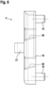
- the Figures 5 to 7 are a plan view and various views of the molding 4 of the in the Figures 1 to 4 Sensor 1 shown can be found.
- the top view of figure 5 in conjunction with the side view of 6 and/or the 7 shows that the molded part 4 essentially has the shape of a flat, elongated cuboid.
- the corners are rounded on the upper side, that is to say on the side which faces away from the support surface 16 .
- On the upper side there is also a web 21 which is arranged approximately in the middle and runs in the transverse direction and which serves as a gripping element.
- the molded part 4 can be gripped and displaced at the web 21 in order to connect it to a carrier element 2, for example.
- the molded part 4 On the underside, that is to say on the support surface 16, the molded part 4 has two pin-shaped connecting means 15 for positive connection with the carrier element 2.
- the molded part 4 also has two window-like recesses 10, 11, which are arranged in the longitudinal direction of the molded part 4 at a distance a from one another.
- the two recesses 10, 11 are offset from one another. The offset in the transverse direction ensures that each guide channel 13, 14 ends in a recess 10, 11 for receiving a connecting wire 7, 8. This is because the offset of the recesses 10, 11 in the transverse direction essentially corresponds to the distance between the two parallel guide channels 13, 14 (see also 7 ).
- the guide channel 13 ends in the recess 10 and the guide channel 14 in the recess 11.
- the distance between the guide channels 13, 14 formed in the molded part 4 can also ensure electrical insulation of the connecting wires 7, 8 be achieved if the molded part 4 is made of an electrically insulating material, in particular plastic.
- the recesses 10, 11 provided in the molded part 4 allow the molded part 4 to be used as a soldering template if an electrical connection between a connecting wire 7, 8 inserted in a guide channel 13, 14 and an electrical connecting surface 5, 6 of a measuring resistor 3 is to be produced by soldering.
- the recesses 10, 11 can each have at least one delimiting flank 26, 27, which runs obliquely in relation to the support surface 16.
- the recesses 10, 11 form a kind of funnel, which simplifies the production of the soldered connection between a connecting wire 7, 8 and an electrical connecting surface 5, 6.
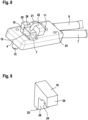
- FIG. 8 and 9 a further preferred embodiment of a molded part 4 according to the invention for the production of an electrical sensor 1 is shown.
- the molded part 4 is characterized by connecting means 20 which are each arranged on two opposite sides of a recess 10, 11 in order to positively connect a pressure piece 19 received in the recess 10, 11 to the molded part 4.
- the pressure piece 19 in turn is used to produce the electrical connection of a connecting wire 7, 8 with an electrical connection surface 5, 6 of the measuring resistor 3 by clamping.
- connecting means 20 for the form-fitting connection of the pressure piece 19 to the molded part 4 is shown in order to keep the drawing clear.
- another connecting means 20 is mirrored on the opposite side of the recess 10 Arrangement provided so that each end of the connecting means 20 arranged latching lugs 28 engage behind the pressure piece 19 and hold it down. In this way, the clamping force required to clamp the connecting wires 7, 8 can be applied.
- a bracket 22 is also indicated, via which the pressure piece 19 is connected or can be connected to a further pressure piece 19 (not shown).
- the bracket 22 facilitates the insertion of the pressure pieces 19 in the recesses 10, 11, since both pressure pieces 19 can be mounted at the same time.
- the bracket 22 can serve as a gripping element in order to lift and move the pressing pieces 19 .
- the molded part 4 of 8 several inflow bores 23, which also pass through the molded part 4.
- the plastic melt can thus get between the molded part 4 and the carrier element 2 . If this is not desired, the inflow bores 23 can also be omitted.
- the 9 is the pressure piece 19 of 8 in a single representation.
- the pressure piece 19 is essentially L-shaped, so that a leg 29 is formed with a support surface 25 on the end face, via which the pressure piece 19 can be supported on the carrier element 2 .
- the other leg 30 of the pressure piece 19 has a guide 24 on its side facing the carrier element 2, in which the connecting wire 7 comes to rest when the pressure piece 19 is inserted into the recess 10 and connected to the molded part 4 via the connecting means 20. In this way it is ensured that the connection wire 7 comes into contact with and thus in electrically conductive contact with the electrical connection surface 5 of the measuring resistor 3 .
- the invention is not limited to the Figures 1 to 9 illustrated preferred embodiments, but also includes modifications within the scope of the claims. These can relate in particular to the specific configuration of the molded part 4 in relation to its connecting means 15 and/or the position, shape and/or size of the recesses 10, 11. Furthermore, the carrier element 2 of a sensor 1 according to the invention can deviate from the representations of Figures 1 to 4 be designed.
Landscapes
- Physics & Mathematics (AREA)
- General Physics & Mathematics (AREA)
- Measuring Temperature Or Quantity Of Heat (AREA)
- Measuring Fluid Pressure (AREA)
- Transmission And Conversion Of Sensor Element Output (AREA)
- Manufacture Of Switches (AREA)
- Push-Button Switches (AREA)
Description
- Die Erfindung betrifft ein Verfahren zur Herstellung eines elektrischen Sensors, insbesondere eines Temperatursensors, mit den Merkmalen des Oberbegriffs des Anspruchs 1. Darüber hinaus betrifft die Erfindung einen elektrischen Sensor mit einem Formteil. Bei dem Formteil handelt es sich demnach um ein Sensorbauteil.
- Aus der
EP 0 905 493 A1 ist ein elektrischer Sensor, insbesondere Temperatursensor bekannt, der einfach aufgebaut ist und weitgehend automatisiert herstellbar sein soll. Er umfasst eine Leiterplatte aus einem elektrisch isolierenden Substrat auf der Basis von temperaturbeständigen Materialien, wie beispielsweise Epoxid, Triazinen, Polyimiden (PI) oder Fluoriden (PTFE). Auf der Vorderseite der Leiterplatte ist ein Bauelement in Form eines SMD-Chips angeordnet, der mittels seiner Kontakte mit Anschlussfeldern der Leiterplatte elektrisch verbunden ist. Die elektrische Verbindung ist durch eine Schmelzverbindung, vorzugsweise durch Verlöten, hergestellt. Von den Anschlussfeldern führen auf der Vorderseite und auf der Rückseite der Leiterplatte angeordnete Leiterbahnen zu Anschlusskontaktfeldern, die der elektrischen Verbindung der Leiterplatte mit den Anschlussleitern eines Anschlusskabels dienen. Die elektrische Verbindung ist auch hier bevorzugt durch eine Schmelzverbindung, insbesondere durch Verlöten, hergestellt. Über eine Kontaktdurchführung im Bereich des SMD-Chips ist die rückseitig angeordnete Leiterbahn mit dem zugehörigen Anschlussfeld auf der Vorderseite der Leiterplatte elektrisch verbunden. - Aus der
EP 0 833 550 A2 sind eine Leiterplatte mit wenigstens einem Bauelement als Messwiderstand, Heizwiderstand oder Messelektroden-Anordnung sowie ein Verfahren zu deren Herstellung bekannt. Verwendung kann die Leiterplatte insbesondere in einem Temperatursensor finden. - Temperatursensoren gehen zudem aus der
EP 1 568 978 A1 sowie derEP 0 547 750 A1 hervor. - Ausgehend von dem vorstehend genannten Stand der Technik liegt der vorliegenden Erfindung die Aufgabe zugrunde, die Herstellung eines elektrischen Sensors, insbesondere eines Temperatursensors, zu vereinfachen. Bei der Herstellung soll zudem ein hoher Automatisierungsgrad erreicht werden. Darüber hinaus soll ein Verfahren angegeben werden, das die Herstellung miniaturisierter elektrischer Sensoren, insbesondere Temperatursensoren, ermöglicht.
- Zur Lösung der Aufgabe werden das Verfahren mit den Merkmalen des Anspruchs 1, sowie der elektrische Sensor mit den Merkmalen des Anspruchs 11 vorgeschlagen. Vorteilhafte Weiterbildungen der Erfindung sind den jeweiligen Unteransprüchen zu entnehmen.
- Bei dem vorgeschlagenen Verfahren zur Herstellung eines elektrischen Sensors, insbesondere eines Temperatursensors, wird ein Trägerelement aus Kunststoff mit einem drahtlosen Messwiderstand in Form eines SMD-Bauteils bestückt, das außenliegende elektrische Anschlussflächen aufweist, wobei das SMD-Bauteil derart auf dem Trägerelement angeordnet und orientiert wird, das die elektrischen Anschlussflächen auf der dem Trägerelement abgewandtem Seite zu liegen kommen. Erfindungsgemäß wird das mit dem Messwiderstand bestückte Trägerelement mit einem Formteil aus Kunststoff verbunden, so dass der Messwiderstand durch das Formteil bereichsweise abgedeckt und gehalten wird und die elektrischen Außenflächen des Messwiderstands zumindest bereichsweise frei liegen. Anschließend wird der Messwiderstand übe die zumindest bereichsweise frei liegenden elektrischen Anschlussflächen mit Anschlussdrähten elektrisch verbunden. Dabei wird das Formteil zur Führung und/oder Positionierung der Anschlussdrähte verwendet und die Führung über im Formteil ausgebildete Führungskanäle bewirkt.
- Der erforderliche elektrische Anschluss des Messwiderstands wird demnach bei dem erfindungsgemäßen Verfahren über Anschlussdrähte hergestellt. Diese werden bis an den Messwiderstand herangeführt und im Bereich frei liegender elektrischer Anschlussflächen des Messwiderstands mit diesem elektrisch verbunden. Das heißt, dass es keiner Leiterplatte mit Leiterbahnen zur Kontaktierung des Messwiderstands bedarf. Ferner können Anschluss- bzw. Anschlusskontaktfelder gemäß dem eingangs genannten Stand der Technik entfallen. Das Trägerelement, das es mit dem Messwiderstand zu bestücken gilt, kann demnach vergleichsweise einfach ausgeführt sein. Zugleich reduziert sich die Anzahl der herzustellenden elektrischen Verbindungen bzw. Kontaktstellen. Folglich kann durch Anwendung des erfindungsgemäßen Verfahrens die Herstellung eines elektrischen Sensors, insbesondere Temperatursensors, vereinfacht werden.
- Der Begriff "Anschlussdraht" umfasst vorliegend auch eine Anschlusslitze, welche aus mehreren Einzeldrähten besteht. Der Einfachheit halber wird nachfolgend jedoch durchgehend von einem "Anschlussdraht" gesprochen, den es mit einer elektrischen Anschlussfläche zu kontaktieren gilt. Ferner kann der Anschlussdraht bzw. die Anschlusslitze eine isolierende Ummantelung aufweisen, die - zumindest im Bereich der herzustellenden Kontaktierung - ggf. zuvor entfernt werden muss. Dieser Verfahrensschritt ist optional und daher nicht gesondert erwähnt.
- Erfindungsgemäß wird bei der Durchführung des erfindungsgemäßen Verfahrens ein drahtloser Messwiderstand in Form eines SMD-Bauteils verwendet, so dass die Herstellung des elektrischen Sensors weiter vereinfacht werden kann. Denn ein SMD-Bauteil weist in der Regel außenliegende elektrische Anschlussflächen auf, die leicht zugänglich und somit einfach zu kontaktieren sind. Das SMD-Bauteil wird hierzu derart auf dem Trägerelement angeordnet bzw. orientiert, dass die elektrischen Anschlussflächen auf der dem Trägerelement abgewandten Seite des Messwiderstands zu liegen kommen. Die Anschlussdrähte können dann über oder auf die elektrischen Anschlussflächen des Messwiderstands gelegt und mit diesen elektrisch verbunden, vorzugsweise verlötet und/oder verklemmt werden. Bevorzugt wird ein in einer Dünnschichttechnologie hergestelltes SMD-Bauteil als drahtloser Messwiderstand verwendet. Derartige SMD-Bauteile sind besonders klein und robust. Zur Herstellung eines Temperatursensors wird bevorzugt ein Platin-Messwiderstand verwendet. Beispielsweise kann ein Platin-Chip-Temperatursensor in SMD-Bauform nach DIN EN 60751 verwendet werden. Dieser kann insbesondere die Form eines flachen Quaders aufweisen, was die Bestückung des Trägerelements mit dem SMD-Bauteil vereinfacht.
- Bei dem erfindungsgemäßen Verfahren wird das mit dem Messwiderstand bestückte Trägerelement mit einem Formteil aus Kunststoff verbunden, und zwar in der Weise, dass der Messwiderstand durch das Formteil abgedeckt wird, aber nur partiell. Denn die elektrischen Anschlussflächen des Messwiderstands müssen zur Herstellung der elektrischen Verbindung mit den Anschlussdrähten - zumindest bereichsweise - frei bleiben. Im Übrigen kann der Messwiderstand durch das Formteil abgedeckt werden, so dass ein Schutz des Messwiderstands vor äußeren Einwirkungen erreicht wird. Dadurch, dass der Messwiderstand durch das Formteil bereichsweise bzw. partiell abgedeckt wird, wird zudem der Messwiderstand auf dem Trägerelement gehalten. Das Formteil weist somit neben der Schutzfunktion ferner eine Haltefunktion bzw. die Funktion eines Bauteilhalters auf. Der Messwiderstand kommt dabei bevorzugt zwischen dem Trägerelement und dem Formteil zu liegen.
- Des Weiteren wird durch das Formteil zugleich eine Lagefixierung des Messwiderstands auf dem Trägerelement erreicht. Durch die Lagefixierung ist die Position des Messwiderstands auf dem Trägerelement bzw. die Lage der elektrischen Anschlussflächen genau vorgegeben, so dass das Heranführen der Anschlussdrähte an die elektrischen Anschlussflächen vereinfacht wird. Insbesondere kann das Heranführen und Positionieren der Anschlussdrähte automatisiert werden. Ferner wird durch die Lagefixierung des Messwiderstands auf dem Trägerelement eine Zugentlastung der hergestellten elektrischen Verbindungen bewirkt.
- Vorteilhafterweise wird das Formteil kraft- und/oder formschlüssig mit dem Trägerelement verbunden. Die kraft- und/oder formschlüssige Verbindung kann beispielsweise durch eine Steck-, Press-, Klemm- und/oder Rastverbindung hergestellt werden. Derartige Verbindungen sind einfach und schnell herstellbar. Dies gilt insbesondere, wenn die kraft- und/oder formschlüssige Verbindung in einem automatisierten Verfahren hergestellt werden soll. Als besonders vorteilhaft wird eine formschlüssige Verbindung des Formteils mit dem Trägerelement angesehen, da der Formschluss die Lage des Formteils in Bezug auf das Trägerelement sichert. Die formschlüssige Verbindung ist somit besonders robust und erleichtert das Handling der verbundenen Bauteile. Beispielsweise kann ein Formschluss durch eine einfache Steckverbindung realisiert werden.
- Ferner bevorzugt wird der Messwiderstand beim Bestücken des Trägerelements in eine Ausnehmung des Trägerelements eingesetzt. Die Ausnehmung gibt die Position des Messwiderstands in Bezug auf das Trägerelement vor. Zugleich verhindert sie eine ungewollte Verschiebung des Messwiderstands gegenüber dem Trägerelement. Die Form der Ausnehmung ist hierzu bevorzugt an die Form des Messwiderstands angepasst. Eine besonders einfache Form des Messwiderstands, beispielsweise eine flache Quaderform, wirkt sich in diesem Fall als Vorteil aus. Vorzugsweise wird der Messwiderstand flächenbündig in die Ausnehmung des Trägerelements eingesetzt, so dass eine ebene Anlagefläche für das Formteil geschaffen wird.
- In Weiterbildung der Erfindung wird vorgeschlagen, dass das Formteil neben den bereits genannten Funktionen mindestens eine weitere Funktion aufweist. Denn - wie nachfolgend aufgezeigt - kann durch Funktionsintegration die Herstellung eines elektrischen Sensors, insbesondere Temperatursensors weiter vereinfacht werden, insbesondere kann der Automatisierungsgrad weiter erhöht werden.
- Des Weiteren wird das Formteil bei der Durchführung des erfindungsgemäßen Verfahrens zur Führung und/oder Positionierung der Anschlussdrähte verwendet. Die Führung wird über im Formteil ausgebildete Führungskanäle bewirkt. Diese sind vorzugsweise in einem Abstand zueinander und/oder parallel verlaufend angeordnet, so dass die Anschlussdrähte durch das Formteil zugleich elektrisch isoliert werden. Hinzu kommt dann noch eine Isolierfunktion des Formteils. Um die Funktion eines Isolierbauteils übernehmen zu können, ist das Formteil bevorzugt aus einem elektrisch isolierenden bzw. elektrisch nichtleitenden Kunststoff hergestellt.
- Die Führungsfunktion des Formteils erleichtert das Heranführen der Anschlussdrähte an die elektrischen Anschlussflächen des Messwiderstands. Um sicherzustellen, dass die Enden der Anschlussdrähte exakt über oder auf den elektrischen Anschlussflächen zu liegen kommen, so dass die erforderliche elektrische Verbindung hergestellt werden kann, wird vorzugsweise das Formteil zugleich als Positionierhilfe eingesetzt. Dank dieser Zusatzfunktionen des Formteils kann die Positionierung der Anschlussdrähte weitgehend automatisiert werden.
- Bevorzugt weist das Formteil eine längliche Bauform auf, wobei die Führungskanäle zur Führung der Anschlussdrähte im Wesentlichen parallel zur Längserstreckung des Formteils verlaufen. Auf diese Weise können maximale Führungslängen erreicht werden. Des Weiteren bevorzugt weist auch das Trägerelement eine längliche Bauform auf, wobei das Formteil und das Trägerelement derart ausgerichtet werden, dass die im Formteil ausgebildeten Führungskanäle im Wesentlichen parallel zur Längserstreckung des Formteils sowie parallel zur Längserstreckung des Trägerelements verlaufen. In mindestens einer Querrichtung zur Längserstreckung des Formteils bzw. des Trägerelements können die Abmessungen minimiert werden, so dass ein besonders kleinvolumiger elektrischer Sensor geschaffen wird.
- In Weiterbildung des erfindungsgemäßen Verfahrens wird ferner vorgeschlagen, dass die Anschlussdrähte im Bereich mindestens einer das Formteil durchsetzenden Ausnehmung mit den elektrischen Anschlussflächen des Messwiderstands elektrisch verbunden werden. Die mindestens eine Ausnehmung ist derart beschaffen, dass sie eine Art Fenster bildet, über welches die elektrische Verbindung mindestens eines Anschlussdrahts mit einer elektrischen Anschlussfläche herstellbar ist. Vorzugsweise ist für jeden Anschlussdraht jeweils eine Ausnehmung bzw. ein Fenster vorgesehen.
- Die Größe und/oder die Lage der mindestens einen Ausnehmung ist bzw. sind durch die Lage der elektrischen Anschlussflächen des Messwiderstands vorgegeben. Denn zur Herstellung einer elektrischen Verbindung eines Anschlussdrahts mit einer elektrischen Anschlussfläche muss die mindestens eine im Formteil ausgebildete Ausnehmung in Überdeckung mit mindestens einer elektrischen Anschlussfläche des Messwiderstands gebracht werden. Ferner muss der Anschlussdraht in der Weise positioniert werden, dass ein Ende des Anschlussdrahts im Bereich der Ausnehmung über oder auf der elektrischen Anschlussfläche zu liegen kommt. Anschließend kann die elektrische Verbindung hergestellt werden. Über die mindestens eine im Formteil ausgebildete Ausnehmung kann somit die exakte Lage der elektrischen Verbindung vorgegeben werden, so dass auch dieser Vorgang automatisiert werden kann.
- Um sicherzustellen, dass die Enden der Anschlussdrähte im Bereich mindestens einer Ausnehmung über oder auf den elektrischen Anschlussflächen zu liegen kommen, wird vorgeschlagen, dass die im Formteil ausgebildeten Führungskanäle zur Führung der Anschlussdrähte in einer Ausnehmung enden. Vorzugsweise endet jeder Führungskanal in einer ihm zugeordneten Ausnehmung. Über eine die Ausnehmung begrenzende und dem Führungskanal gegenüber liegende Wandfläche ist dann die jeweilige Endlage eines Anschlussdrahts vorgegeben.
- Wird das Formteil von mehreren Ausnehmungen, vorzugsweise von zwei Ausnehmungen, durchsetzt, sind diese bevorzugt in einem Abstand zueinander und/oder versetzt zueinander angeordnet. Der Abstand der Ausnehmungen zueinander wird vorzugsweise in Längsrichtung der Anschlussdrähte bzw. der im Formteil ausgebildeten Führungskanäle gemessen. Das heißt, dass die Führungskanäle unterschiedlich lang ausgebildet sind. Auf diese Weise wird eine räumliche Entzerrung der elektrischen Anschlussstellen bewirkt. Ferner wird die Gefahr eines elektrischen Kurzschlusses beseitigt oder zumindest minimiert. Über einen Versatz der Ausnehmungen zueinander kann einem Abstand der Führungskanäle zueinander Rechnung getragen werden.
- In Weiterbildung des erfindungsgemäßen Verfahrens wird ferner vorgeschlagen, dass die Anschlussdrähte durch Verlöten und/oder Verklemmen mit den elektrischen Anschlussflächen des Messwiderstands elektrisch verbunden werden.
- Soll die elektrische Verbindung durch Verlöten hergestellt werden, kann das Formteil als "Lötlehre" verwendet werden. Das Lot zur Herstellung der Lötverbindung wird hierzu im Bereich einer das Formteil durchsetzenden Ausnehmung eingebracht. Durch die Ausnehmung ist somit die exakte Lage der Lötverbindung vorgegeben, so dass auch dieser Verfahrensschritt automatisiert werden kann.
- Alternativ oder ergänzend kann die elektrische Verbindung durch Verklemmen hergestellt werden. Bevorzugt wird hierzu mindestens ein Druckstück verwendet, das in eine Ausnehmung des Formteils eingesetzt und mit dem Formteil kraft- und/oder formschlüssig verbunden wird, so dass mindestens ein Anschlussdraht gegen eine elektrische Anschlussfläche des Messwiderstands gedrückt wird. Über die kraft- und/oder formschlüssige Verbindung des Druckstücks mit dem Formteil kann die erforderliche Druck- bzw. Klemmkraft aufgebracht werden.
- Das Druckstück kann bereits mit dem Formteil verbunden sein, beispielsweise über ein Scharnier oder Gelenk. In diesem Fall muss das Druckstück zum Einsetzen in die Ausnehmung des Formteils nur noch verschwenkt werden. Sofern mehrere Druckstücke vorgesehen sind, können diese untereinander verbunden sein, so dass sie als Einheit in das Formteil einsetzbar sind. Die Verbindung kann beispielsweise über eine Art Bügel bewirkt werden, welcher zugleich das Handling der mehrere Druckstücke umfassenden Einheit vereinfacht.
- Die kraft- und/oder formschlüssige Verbindung des mindestens einen Druckstücks mit dem Formteil kann in einfacher Weise über eine Steck-, Press-, Klemm- und/oder Rastverbindung hergestellt werden. Beispielsweise können im Bereich einer Ausnehmung zur Aufnahme eines Druckstücks Klemm- und/oder Rastmittel vorgesehen sein, wobei vorzugsweise die Rastmittel das Druckstück hinter- oder umgreifen, so dass ein Formschluss erreicht wird. Sind Rastmittel vorgesehen, die das Druckstück an zwei sich gegenüberliegenden Seiten hinter- bzw. umgreifen, kann hierüber eine Druckkraft erzeugt werden, die ein gleichmäßiges Andrücken eines Anschlussdrahts an eine elektrische Anschlussfläche gewährleistet.
- Bevorzugt sind für jeden Anschlussdraht eine das Formteil durchsetzende Ausnehmung sowie ein in die Ausnehmung einsetzbares Druckstück vorgesehen. Ferner bevorzugt verfügt zudem jede Ausnehmung über Rastmittel, die an sich gegenüberliegenden Seiten angeordnet sind und das in die Ausnehmung eingesetzte Druckstück hinter- oder umgreifen. Die Rastmittel können hierzu jeweils nach Art eines Federarms ausgebildet sein, der eine gewisse Nachgiebigkeit besitzt, um das Einsetzen des Druckstücks in die Ausnehmung zu ermöglichen. Nach dem Einsetzen nimmt das Rastmittel seine ursprüngliche Form/Position ein und verrastet hinter dem Druckstück.
- In Weiterbildung des erfindungsgemäßen Verfahrens wird darüber hinaus vorgeschlagen, dass nach dem elektrischen Verbinden der Anschlussdrähte mit den elektrischen Anschlussflächen des Messwiderstands das Trägerelement, der Messwiderstand und/oder das Formteil zumindest bereichsweise mit einem Kunststoff umspritzt werden. In Abhängigkeit von der konkreten Ausgestaltung der Kunststoff-Umspritzung bildet diese eine Schutzhülle aus, welche den Messwiderstand vor äußeren Einwirkungen schützt. Zugleich kann eine Abdichtung erreicht werden. Ein derart hergestellter elektrischer Sensor ist demnach besonders robust und somit vielseitig einsetzbar. Sofern es sich bei dem elektrischen Sensor um einen Temperatursensor handelt, wird vorzugsweise ein thermisch leitfähiger Kunststoff zum Umspritzen verwendet. Auf diese Weise bleibt eine schnelle Ansprechbarkeit des Temperatursensors erhalten.
- Alternativ oder ergänzend zu einer Umspritzung mit Kunststoff können das Trägerelement, der Messwiderstand und das Formteil in ein Gehäuse eingesetzt werden. Durch ein Gehäuse kann insbesondere die Robustheit des Sensors gegenüber mechanischen Beeinträchtigungen und/oder gegenüber aggressiven Medien erhöht werden.
- Vorteilhafterweise wird das erfindungsgemäße Verfahren in einzelnen oder in allen seinen Schritten automatisiert durchgeführt. Über einen hohen Grad der Automatisierung können die Herstellungskosten gesenkt werden. Bevorzugt wird das erfindungsgemäße Verfahren in einem Bestückungsautomaten durchgeführt. Das bei der Durchführung des Verfahrens eingesetzte Formteil kann dabei die Funktion eines Bauteilhalters, eines Führungselements, einer Positionierhilfe, eines Isolierbauteils und/oder einer Lötlehre übernehmen.
- Bei dem erfindungsgemäßen Verfahren wird bzw. werden bevorzugt ein Trägerelement und/oder ein Formteil aus einem elektrisch isolierenden und thermisch leitfähigen Kunststoff verwendet. Dies gilt im Besonderen, wenn das Verfahren der Herstellung eines Temperatursensors dient. Die Verwendung eines thermisch leitfähigen Kunststoffs gewährleistet eine schnelle Ansprechbarkeit und eine hohe Messgenauigkeit des Temperatursensors.
- Zur Lösung der eingangs genannten Aufgabe wird ferner ein elektrischer Sensor, insbesondere Temperatursensor, mit einem Formteil vorgeschlagen. Das Formteil zeichnet sich dadurch aus, dass es
- aus Kunststoff, insbesondere aus einem elektrisch isolierenden und thermisch leitfähigen Kunststoff, hergestellt ist,
- von mindestens einer Ausnehmung durchsetzt ist,
- mindestens einen Führungskanal aufweist, der vorzugsweise in einer das Formteil durchsetzenden Ausnehmung endet,
- und Verbindungsmittel zur kraft- und/oder formschlüssigen Verbindung mit einem Trägerelement aufweist, und in dem mindestens einen Führungskanal des Formteils ein Anschlussdraht eingelegt ist, der im Bereich der Ausnehmung mit einer elektrischen Anschlussfläche des Messwiderstands elektrisch verbunden, vorzugsweise verlötet und/oder verklemmt, ist.
- Das Formteil weist somit alle Ausstattungsmerkmale auf, die den Einsatz des Formteils in dem zuvor beschriebenen erfindungsgemäßen Verfahren ermöglichen. Erfindungsgemäß ist das Formteil über die Verbindungmittel mit einem Trägerelement verbunden, das zuvor mit einem Messwiderstand, vorzugsweise in Form eines SMD-Bauteils, bestückt worden ist. Das Formteil kommt dann als Bauteilhalter zum Einsatz. Über den mindestens einen im Formteil ausgebildeten Führungskanal wird ein Anschlussdraht an den Messwiderstand herangeführt und anschließend im Bereich der Ausnehmung mit der elektrischen Anschlussfläche des Messwiderstands elektrisch verbunden, insbesondere verlötet und/oder verklemmt. Das Formteil kann demnach ferner als Führungselement, Positionierhilfe und/oder als Lötlehre verwendet werden.
- In der Ausführung als Kunststoffteil ist das Formteil zudem einfach und kostengünstig herstellbar. Bei Verwendung eines elektrisch isolierenden und thermisch leitfähigen Kunststoffs kann das Formteil zugleich als Isolierbauteil eingesetzt werden.
- Die Verbindungsmittel zur Verbindung des Formteils mit dem Trägerelement umfassen vorzugsweise mindestens zwei stiftförmig ausgeführte Verbindungsmittel, die in korrespondierend hierzu ausgebildete Ausnehmungen des Trägerelements einsetzbar sind. Über die in die Ausnehmungen eingreifenden stiftförmigen Verbindungsmittel ist ein Formschluss bewirkbar, der eine Verschiebung des Formteils gegenüber dem Trägerelement verhindert. Dadurch, dass mindestens zwei stiftförmige Verbindungsmittel vorgesehen sind, wird zugleich eine Verdrehsicherung des Formteils bewirkt. Weiterhin bevorzugt sind die Verbindungsmittel an einer Stützfläche des Formteils angeordnet, über die das Formteil am Trägerelement abstützbar ist. Über die Abstützung des Formteils am Trägerelement kann zugleich eine Lagefixierung des Messwiderstands auf dem Trägerelement erreicht werden.
- Weiterhin bevorzugt weist das Formteil mindestens zwei Ausnehmungen auf, die das Formteil durchsetzen. Die Ausnehmungen stellen sicher, dass nach dem Verbinden des Formteils mit dem Trägerelement, die elektrischen Anschlussflächen eines auf dem Trägerelement angeordneten Messwiderstands zumindest bereichsweise freigelegt sind. Die Ausnehmungen sind hierzu bevorzugt in einem Abstand zueinander und/oder versetzt zueinander angeordnet. Jede Ausnehmung kann somit einer elektrischen Anschlussfläche des Messwiderstands bzw. einem Anschlussdraht zugeordnet werden. Ferner kann im Bereich einer Ausnehmung eine elektrische Verbindung eines Anschlussdrahts mit einer elektrischen Anschlussfläche des Messwiderstands hergestellt werden.
- Vorteilhafterweise besitzt das Formteil eine längliche Form. Die längliche Form begünstigt die Ausbildung eines Abstands zwischen den das Formteil durchsetzenden Ausnehmungen. Ferner bevorzugt weist das Formteil eine flache Bauform auf, wobei die Ausnehmungen das Formteil in Richtung seiner geringsten Ausdehnung durchsetzen. Die Ausnehmungen bilden somit Fenster aus, welche die Zugänglichkeit der elektrischen Anschlussflächen des Messwiderstands gewährleisten, um den erforderlichen elektrischen Anschluss herstellen zu können.
- Des Weiteren bevorzugt sind mindestens zwei Führungskanäle vorgesehen, die in einem Abstand zueinander und/oder parallel verlaufend angeordnet sind. Jeder Führungskanal kann zur Führung und/oder Positionierung eines Anschlussdrahts verwendet werden. Über den Abstand der Führungskanäle zueinander kann zugleich eine elektrische Isolierung der Anschlussdrähte bewirkt werden.
- Ferner wird vorgeschlagen, dass jeder Führungskanal in einer das Formteil durchsetzenden Ausnehmung endet. Über die Ausnehmung ist somit die Endlage eines Anschlussdrahts vorgebbar. Dadurch ist sichergestellt, dass das Ende eines Anschlussdrahts exakt über oder auf einer elektrischen Anschlussfläche des Messwiderstands zu liegen kommt, um die erforderliche elektrische Verbindung herzustellen.
- Die Führungskanäle verlaufen bevorzugt parallel zur Längserstreckung des Formteils, so dass große Führungslängen erzielt werden. Die das Formteil durchsetzenden Ausnehmungen, in denen die Führungskanäle enden, sind vorzugsweise senkrecht hierzu geführt. Weiterhin vorzugsweise sind die Ausnehmungen in einem Abstand zueinander bzw. in Längsrichtung der Führungskanäle hintereinander liegend angeordnet, so dass die in diesen Ausnehmungen endenden Führungskanäle unterschiedlich lang ausgeführt sind. Auf diese Weise wird eine räumliche Entzerrung der elektrischen Anschlussstellen erreicht.
- Der elektrische Anschluss bzw. die elektrische Verbindung kann insbesondere durch Verlöten und/oder Verklemmen hergestellt werden. Die zum Verklemmen erforderliche Klemmkraft kann dabei über mindestens ein Druckstück aufgebracht werden, das vorzugsweise in eine Ausnehmung des Formteils eingesetzt und mit dem Formteil kraft- und/oder formschlüssig verbunden wird.
- In Weiterbildung der Erfindung wird daher vorgeschlagen, dass das Formteil Verbindungsmittel zur kraft- und/oder formschlüssigen Verbindung mit mindestens einem Druckstück aufweist. Vorzugsweise entspricht die Anzahl der Druckstücke der Anzahl der Anschlussdrähte, so dass jeder Anschlussdraht (bzw. jede Anschlusslitze) separat verklemmbar ist. Weiterhin vorzugsweise sind die zur kraft- und/oder formschlüssigen Verbindung mit dem Druckstück vorgesehenen Verbindungsmittel im Bereich mindestens einer das Formteil durchsetzenden Ausnehmung angeordnet. Das Druckstück kann dann in die Ausnehmung eingesetzt beim Einsetzen in die Ausnehmung mit dem Formteil kraft- und/oder formschlüssig verbunden werden. Vorzugsweise wird über die Verbindungsmittel eine Steck-, Press-, Klemm- und/oder Rastverbindung. Zur Realisierung einer Rastverbindung weisen die Verbindungsmittel bevorzugt Rastmittel auf, die das in die Ausnehmung eingesetzte Druckstück hinter- oder umgreifen. Dadurch ist sichergestellt, dass eine über das Druckstück auf einen Anschlussdraht aufgebrachte Druck- bzw. Klemmkraft dauerhaft erhalten bleibt.
- Ein zum Verklemmen einsetzbares Druckstück kann auch bereites mit dem Formteil verbunden sein, beispielsweise über ein Scharnier oder Gelenk. Das Scharnier oder Gelenk erlaubt ein Verschwenken des Druckstücks gegenüber dem Formteil, um es in eine Ausnehmung des Formteils einzusetzen. Anschließend muss das Druckstück in seiner Lage gesichert werden, um die erforderliche Klemmkraft aufzubringen. Die Lagesicherung kann mittels einer kraft- und/oder formschlüssigen Verbindung des Druckstücks mit dem Formteil erreicht werden.
- Sofern mehrere Druckstücke vorgesehen sind, die nicht bereits mit dem Formteil verbunden sind, können diese untereinander verbunden werden. Beispielsweise über eine Art Bügel, der zugleich als Griffelement nutzbar ist und das Einsetzen der Druckstücke in die Ausnehmungen erleichtert.
- Erfindungsgemäß ist das Formteil kraft- und/oder formschlüssig mit einem Trägerelement aus Kunststoff verbunden, das mit einem Messwiderstand, vorzugsweise in Form eines SMD-Bauteils, bestückt ist. Das Formteil besitzt die Funktion, den Messwiderstand bzw. das SMD-Bauteil in Position zu halten. Das Formteil dient demnach als Bauteilhalter.
- Der vorgeschlagene elektrische Sensor, insbesondere Temperatursensor, ist vorzugsweise nach dem zuvor beschriebenen erfindungsgemäßen Verfahren hergestellt worden. Die Herstellung nach dem erfindungsgemäßen Verfahren und/oder die Verwendung eines erfindungsgemäßen Formteils bei der Herstellung ermöglichen einen hohen Automatisierungsgrad, so dass die Herstellungskosten gesenkt werden können.
- Erfindungsgemäß ist in dem mindestens einen Führungskanal des Formteils ein Anschlussdraht (bzw. eine Anschlusslitze) eingelegt, der im Bereich der Ausnehmung mit einer elektrischen Anschlussfläche des Messwiderstands elektrisch verbunden, vorzugsweise verlötet und/oder verklemmt, ist. In dieser Ausgestaltung eines elektrischen Sensors kommen gleich mehrere Funktionen des Formteils bei der Herstellung des Sensors zum Tragen. Insbesondere kann das Formteil als Führungselement, Positionierhilfe und/oder Lötlehre eingesetzt werden.
- Des Weiteren kann das Formteil als Isolierbauteil zur elektrischen Isolierung des Anschlussdrahts (bzw. der Anschlusslitze) von mindestens einem weiteren Anschlussdraht (bzw. einer weiteren Anschlusslitze) eingesetzt werden, wenn dieser in einen weiteren Führungskanal eingelegt ist, der vorzugsweise in einem Abstand und/oder parallel verlaufend zum ersten Führungskanal angeordnet ist.
- Idealerweise ist bzw. sind daher das Trägerelement und/oder das Formteil aus einem elektrisch isolierenden und thermisch leitfähigen Kunststoff hergestellt.
- Zum Schutz des erfindungsgemäßen elektrischen Sensors vor äußeren Einwirkungen wird vorgeschlagen, dass das Trägerelement, der Messwiderstand und/oder das Formteil zumindest bereichsweise mit einem Kunststoff umspritzt und/oder von einem Gehäuse umgeben sind. Die Maßnahmen tragen - einzeln oder in Kombination - dazu bei, dass der Messwiderstand optimal vor äußeren Einwirkungen geschützt ist, insbesondere kann eine Abdichtung erreicht werden. Entsprechend steigt die Robustheit des elektrischen Sensors, der somit vielseitig einsetzbar ist.
- Handelt es sich bei dem elektrischen Sensor um einen Temperatursensor, sind vorzugsweise das Trägerelement, der Messwiderstand und/oder das Formteil zumindest bereichsweise mit einem thermisch leitfähigem, Kunststoff umspritzt. Der thermisch leitfähige Kunststoff trägt dazu bei, dass der Sensor eine schnelle Ansprechbarkeit und eine hohe Messgenauigkeit aufweist.
- Die Erfindung wird nachfolgend anhand der beigefügten Zeichnungen näher erläutert. Die Zeichnungen zeigen:
- Fig. 1
- eine Draufsicht auf einen elektrischen Sensor gemäß einer bevorzugten Ausführungsform der Erfindung vor dem Umspritzen mit Kunststoff,
- Fig. 2
- eine perspektivische Darstellung des elektrischen Sensors der
Fig. 1 , - Fig.3
- einen Querschnitt durch den elektrischen Sensor der
Fig. 1 , - Fig. 4
- eine Seitenansicht auf den elektrischen Sensor der
Fig. 1 nach dem Umspritzen mit Kunststoff, - Fig. 5
- eine Draufsicht auf das Formteil des elektrischen Sensors der
Fig. 1 , - Fig. 6
- eine Seitenansicht des Formteils des elektrischen Sensors der
Fig. 1 , - Fig. 7
- eine Seitenansicht des Formteils des elektrischen Sensors der
Fig. 1 um 90° gedreht, - Fig. 8
- eine perspektivische Darstellung eines abgewandelten erfindungsgemäßen Formteils mit Druckstück zum Verklemmen eines Anschlussdrahts und
- Fig. 9
- eine perspektivische Darstellung des Druckstücks der
Fig. 8 . - Der in der
Fig. 1 dargestellte elektrische Sensor 1 umfasst ein längliches, im Querschnitt halbkreisförmiges Trägerelement 2, das mit einem Messwiderstand 3 bestückt ist. Bei dem Messwiderstand 3 handelt es sich um ein SMD-Bauteil, das keine Anschlussdrähte, sondern elektrische Anschlussflächen 5, 6 aufweist. Das SMD-Bauteil ist in eine Ausnehmung 9 des Trägerelements 2 flächenbündig eingesetzt (sieheFig. 3 ). - Zur weiteren Lagefixierung des SMD-Bauteils ist auf das Trägerelement 2 ein Formteil 4 mit Ausnehmungen 10, 11 aufgesteckt, so dass die Ausnehmungen 10, 11 im Bereich der elektrischen Anschlussflächen 5, 6 des Messwiderstands 3 zu liegen kommen. Die fensterartigen Ausnehmungen 10, 11 dienen der Freilegung der elektrischen Anschlussflächen 5, 6, um diese mit Anschlussdrähten 7, 8 elektrisch verbinden zu können, die in Führungskanälen 13, 14 des Formteils 4 aufgenommen sind. Die elektrische Verbindung kann beispielsweise durch Verlöten hergestellt werden. Die Steckverbindung des Formteils 4 mit dem Trägerelement 2 ist über stiftförmige Verbindungsmittel 15 hergestellt, die auf einer dem Trägerelement 2 zugewandten Stützfläche 16 des Formteils 4 ausgebildet sind und in entsprechende Ausnehmungen 17 des Trägerelements 2 eingreifen.
- Die Führungskanäle 13, 14 erstrecken sich in Längsrichtung des Formteils 4 und sind in einem Abstand parallel zueinander geführt. Der den Anschlussdraht 7 aufnehmende Führungskanal 13 ist länger als der den Anschlussdraht 8 aufnehmende Führungskanal 14 ausgeführt, da der Messwiderstand 3 in der Weise orientiert ist, dass die die elektrischen Anschlussflächen 5, 6 in Längsrichtung des Formteils 4 hintereinander zu liegen kommen. Dadurch wird eine räumliche Entzerrung der elektrischen Anschlussstellen bewirkt, so dass die Gefahr eines Kurzschlusses beseitigt wird. Entsprechend sind auch die beiden fensterartigen Ausnehmungen 10, 11 des Formteils 4 in einem Abstand zueinander angeordnet. Darüber hinaus sind die Ausnehmungen 10, 11 in Querrichtung des Formteils 4 versetzt zueinander angeordnet, was dem Umstand Rechnung trägt, dass die Führungskanäle 13, 14 zur elektrischen Isolierung der hierin aufgenommenen Anschlussdrähte 7, 8 in einem Abstand zueinander parallel verlaufen.
- Wie insbesondere der
Fig. 3 zu entnehmen ist, kommen die in den Führungskanälen 13, 14 aufgenommenen Anschlussdrähte 7, 8 über den elektrischen Anschlussflächen 5, 6 des Messwiderstands 3 zu liegen. Das heißt, dass ein gewisser Spalt zur Herstellung der elektrischen Verbindung mittels Verlöten verbleibt. Nach dem Verlöten wird der Spalt von dem Lot (nicht dargestellt) ausgefüllt. -
Fig. 2 zeigt, dass das Trägerelement 2 deutlich länger als das Formteil ausgeführt sein kann. Im Bereich der Verlängerung weist das Trägerelement 2 vorliegend Führungsstege 18 auf, zwischen denen die Anschlussdrähte 7, 8 eingelegt sind. - Somit wird eine zusätzliche Führung der Anschlussdrähte 7, 8 über das Trägerelement 2 erreicht.
- Die Führung der Anschlussdrähte 7, 8 erweist sich insbesondere bei der Herstellung des Sensors 1 als Vorteil. Denn aufgrund der Führung können die Anschlussdrähte 7, 8 eingeschossen werden, so dass die Herstellung des Sensors 1 zumindest weitgehend automatisiert werden kann.
- Vorzugsweise wird bei der Herstellung des Sensors 1 erst der Messwiderstand 3 in die Ausnehmung 9 des Trägerelements 2 eingesetzt, anschließend das Formteil 4 auf das Trägerelement 2 aufgesteckt. Danach werden die Anschlussdrähte 7, 8 eingeschossen, wobei das Formteil 4 als Führungselement und Positionierhilfe dient. Denn über die Führungskanäle 13, 14 und die fensterartigen Ausnehmungen 10, 11 ist die jeweilige Lage, insbesondere Endposition, der Anschlussdrähte 7, 8 genau vorgegeben. Die Enden der Anschlussdrähte 7, 8 kommen genau über den elektrischen Anschlussflächen 5, 6 des Messwiderstands 3 zu liegen, so dass über die fensterartigen Ausnehmungen 10, 11 die elektrische Verbindung durch Verlöten hergestellt werden kann. Das Formteil 4 dient dabei als Lötlehre. Die Herstellung des Sensors kann somit vollständig automatisiert werden.
- Abschließend kann der Sensor 1 mit Kunststoff 12 umspritzt bzw. teilumspritzt werden, wobei es sich vorzugsweise um einen elektrisch isolierenden und thermisch leitfähigen Kunststoff 12 handelt. Der Sensor 1 der
Fig. 1 mit einer entsprechenden Teilumspritzung aus Kunststoff 12 ist beispielhaft in derFig. 4 dargestellt. Der Kunststoff 12 ist derart an das Trägerelement 2 angespritzt, dass das Formteil 4 vollständig von Kunststoff 12 umgeben ist. Auf diese Weise wird eine optimale Abdichtung erreicht. Durch die Teilumspritzung aus Kunststoff 12 weist der Sensor 1 einen kreisförmigen Querschnitt auf. Dies erleichtert das Einsetzen des Sensors 1 in ein Gehäuse 31, sofern erwünscht. Ein Gehäuse 31 ist optional und kann alternativ oder ergänzend zu einer Umspritzung mit Kunststoff 12 vorgesehen sein. - Den
Figuren 5 bis 7 sind eine Draufsicht und verschiedene Ansichten des Formteils 4 des in denFiguren 1 bis 4 dargestellten Sensors 1 zu entnehmen. - Die Draufsicht der
Fig. 5 in Verbindung mit der Seitenansicht derFig. 6 und/oder derFig. 7 zeigt, dass das Formteil 4 im Wesentlichen die Form eines flachen länglichen Quaders besitzt. Oberseitig, das heißt auf der Seite, die der Stützfläche 16 abgewandt ist, sind die Ecken abgerundet. Auf der Oberseite ist zudem ein in etwa mittig angeordneter und in Querrichtung verlaufender Steg 21 angeordnet, der als Griffelement dient. An dem Steg 21 kann das Formteil 4 gegriffen und versetzt werden, um es beispielweise mit einem Trägerelement 2 zu verbinden. Unterseitig, das heißt an der Stützfläche 16, weist das Formteil 4 zwei stiftförmige Verbindungsmittel 15 zur formschlüssigen Verbindung mit dem Trägerelement 2 auf. - Wie insbesondere der
Fig. 5 zu entnehmen ist, besitzt das Formteil 4 ferner zwei fensterartige Ausnehmungen 10, 11, die in Längsrichtung des Formteils 4 in einem Abstand a zueinander angeordnet sind. In Querrichtung des Formteils 4 sind die beiden Ausnehmungen 10, 11 versetzt zueinander angeordnet. Durch den Versatz in Querrichtung ist sichergestellt, dass jeder Führungskanal 13, 14 zur Aufnahme eines Anschlussdrahts 7, 8 in einer Ausnehmung 10, 11 endet. Denn der Versatz der Ausnehmungen 10, 11 in Querrichtung entspricht im Wesentlichen dem Abstand der beiden parallel geführten Führungskanäle 13, 14 zueinander (siehe auchFig. 7 ). - Vorliegend endet der Führungskanal 13 in der Ausnehmung 10 und der Führungskanal 14 in der Ausnehmung 11.
- Da das Formteil 4 aus einem elektrisch nicht leitenden Kunststoff hergestellt ist, kann über den Abstand der im Formteil 4 ausgebildeten Führungskanäle 13, 14 zugleich eine elektrische Isolierung der hierin eingelegten Anschlussdrähte 7, 8 erreicht werden, sofern das Formteil 4 aus einem elektrisch isolierenden Werkstoff, insbesondere Kunststoff hergestellt ist.
- Die im Formteil 4 vorgesehenen Ausnehmungen 10, 11 ermöglichen eine Verwendung des Formteils 4 als Lötlehre, wenn durch Verlöten eine elektrische Verbindung eines in einen Führungskanal 13, 14 eingelegten Anschlussdrahts 7, 8 mit einer elektrischen Anschlussfläche 5, 6 eines Messwiderstands 3 hergestellt werden soll. Wie in den
Figuren 5 bis 7 dargestellt können die Ausnehmungen 10, 11 jeweils mindestens eine begrenzende Flanke 26, 27 aufweisen, die schräg in Bezug auf die Stützfläche 16 verläuft. Dadurch bilden die Ausnehmungen 10, 11 eine Art Trichter aus, der das Herstellen der Lötverbindung zwischen einem Anschlussdraht 7, 8 und einer elektrischen Anschlussfläche 5, 6 vereinfacht. - In den
Figuren 8 und 9 ist eine weitere bevorzugte Ausführungsform eines erfindungsgemäßen Formteils 4 zur Herstellung eines elektrischen Sensors 1 dargestellt. Das Formteil 4 zeichnet sich durch Verbindungsmittel 20 aus, die jeweils an zwei sich gegenüberliegenden Seiten einer Ausnehmung 10, 11 angeordnet sind, um ein in der Ausnehmung 10, 11 aufgenommenes Druckstück 19 mit dem Formteil 4 formschlüssig zu verbinden. Das Drückstück 19 wiederum dient der Herstellung der elektrischen Verbindung eines Anschlussdrahts 7, 8 mit einer elektrischen Anschlussfläche 5, 6 des Messwiderstands 3 durch Verklemmen. - Der Einfachheit halber ist in der
Fig. 8 nur ein Druckstück 19 dargestellt, das in die Ausnehmung 10 eingesetzt ist. Analog ist vorzugsweise ein weiteres Druckstück 19 in die Ausnehmung 11 eingesetzt (nicht dargestellt). - Ferner ist im Bereich der Ausnehmung 10 nur ein Verbindungsmittel 20 zur formschlüssigen Verbindung des Druckstücks 19 mit dem Formteil 4 dargestellt, um die Zeichnung übersichtlich zu halten. Vorzugsweise ist auf der gegenüberliegenden Seite der Ausnehmung 10 ein weiteres Verbindungsmittel 20 in gespiegelter Anordnung vorgesehen, so dass jeweils endseitig an den Verbindungsmitteln 20 angeordnete Rastnasen 28 das Druckstück 19 hintergreifen und niederhalten. Auf diese Weise kann die zum Verklemmen der Anschlussdrähte 7, 8 erforderliche Klemmkraft aufgebracht werden.
- In der
Fig. 8 ist ferner ein Bügel 22 angedeutet, über den das Druckstück 19 mit einem weiteren Druckstück 19 (nicht dargestellt) verbunden bzw. verbindbar ist. Der Bügel 22 erleichtert das Einsetzen der Druckstücke 19 in die Ausnehmungen 10, 11, da beide Druckstücke 19 gleichzeitig montiert werden können. Der Bügel 22 kann dabei als Griffelement dienen, um die Drückstücke 19 anzuheben und zu versetzen. - Neben den Ausnehmungen 10, 11 weist das Formteil 4 der
Fig. 8 mehrere Zuflussbohrungen 23 auf, die das Formteil 4 ebenfalls durchsetzen. Beim Umspritzen mit Kunststoff kann somit die Kunststoffschmelze zwischen das Formteil 4 und das Trägerelement 2 gelangen. Ist dies nicht erwünscht, können die Zuflussbohrungen 23 auch entfallen. - Der
Fig. 9 ist das Druckstück 19 derFig. 8 in einer Einzeldarstellung zu entnehmen. Das Druckstück 19 ist vorliegend im Wesentlichen L-förmig ausgeführt, so dass ein Schenkel 29 mit einer stirnseitigen Stützfläche 25 ausgebildet wird, über welche das Druckstück 19 an dem Trägerelement 2 abstützbar ist. Denn das Druckstück 19 wird vorzugsweise erst in die Ausnehmung 10 eingesetzt, nachdem das Formteil 4 mit dem Trägerelement 2 verbunden worden ist. Der andere Schenkel 30 des Druckstücks 19 weist auf seiner dem Trägerelement 2 zugewandten Seite eine Führung 24 auf, in welcher der Anschlussdraht 7 zu liegen kommt, wenn das Druckstück 19 in die Ausnehmung 10 eingesetzt und über die Verbindungsmittel 20 mit dem Formteil 4 verbunden wird. Auf diese Weise ist sichergestellt, dass der Anschlussdraht 7 zur Anlage und damit in elektrisch leitendem Kontakt mit der elektrischen Anschlussfläche 5 des Messwiderstands 3 gelangt. - Die Erfindung ist nicht auf die in den
Figuren 1 bis 9 dargestellten bevorzugten Ausführungsformen beschränkt, sondern schließt im Umfang der Ansprüche auch Abwandlungen mit ein. Diese können insbesondere die konkrete Ausgestaltung des Formteils 4 in Bezug auf seine Verbindungsmittel 15 und/oder die Lage, Form und/oder die Größe der Ausnehmungen 10, 11 betreffen. Ferner kann das Trägerelement 2 eines erfindungsgemäßen Sensors 1 abweichend von den Darstellungen derFig. 1 bis 4 gestaltet sein. -
- 1
- Sensor
- 2
- Trägerelement
- 3
- Messwiderstand
- 4
- Formteil
- 5
- Anschlussfläche
- 6
- Anschlussfläche
- 7
- Anschlussdraht
- 8
- Anschlussdraht
- 9
- Ausnehmung
- 10
- Ausnehmung
- 11
- Ausnehmung
- 12
- Kunststoff, Kunststoff-Umspritzung
- 13
- Führungskanal
- 14
- Führungskanal
- 15
- Verbindungsmittel
- 16
- Stützfläche
- 17
- Ausnehmung
- 18
- Führungssteg
- 19
- Druckstück
- 20
- Verbindungsmittel
- 21
- Steg, Griffelement
- 22
- Bügel, Griffelement
- 23
- Zuflussbohrung
- 24
- Führung
- 25
- Stützfläche
- 26
- Flanke
- 27
- Flanke
- 28
- Rastnase
- 29
- Schenkel
- 30
- Schenkel
- 31
- Gehäuse
Claims (17)
- Verfahren zur Herstellung eines elektrischen Sensors (1), insbesondere eines Temperatursensors, bei dem ein Trägerelement (2) aus Kunststoff mit einem drahtlosen Messwiderstand (3) in Form eines SMD-Bauteils bestückt wird, das außenliegende elektrische Anschlussflächen (5,6) aufweist, wobei das SMD-Bauteil derart auf dem Trägerelement (2) angeordnet und orientiert wird, dass die elektrischen Anschlussflächen (5, 6) auf der dem Trägerelement (2) abgewandten Seite zu liegen kommen,
wobei
das mit dem Messwiderstand (3) bestückte Trägerelement (2) mit einem Formteil (4) aus Kunststoff verbunden wird, so dass der Messwiderstand (3) durch das Formteil (4) bereichsweise abgedeckt und gehalten wird und die elektrischen Anschlussflächen (5, 6) des Messwiderstands (3) zumindest bereichsweise frei liegen, anschließend der Messwiderstand (3) über die zumindest bereichsweise frei liegenden elektrischen Anschlussflächen (5, 6) mit Anschlussdrähten (7, 8) elektrisch verbunden wird, wobei das Formteil (4) zur Führung und/oder Positionierung der Anschlussdrähte (7, 8) verwendet wird und die Führung über im Formteil (4) ausgebildete Führungskanäle (13, 14) bewirkt wird. - Verfahren nach Anspruch 1,
wobei
das Formteil (4) kraft- und/oder formschlüssig mit dem Trägerelement (2) verbunden wird, beispielsweise durch eine Steck-, Press-, Klemm- und/oder Rastverbindung. - Verfahren nach Anspruch 1 oder 2,
wobei
der Messwiderstand (3) beim Bestücken des Trägerelements (2), vorzugsweise flächenbündig, in eine Ausnehmung (9) des Trägerelements (2) eingesetzt wird. - Verfahren nach einem der vorhergehenden Ansprüche, sz
wobei
die im Formteil (4) ausgebildeten Führungskanäle (13, 14) in einem Abstand zueinander und/oder parallel verlaufend angeordnet sind, so dass die Anschlussdrähte (7, 8) durch das Formteil (4) elektrisch isoliert werden. - Verfahren nach einem der vorhergehenden Ansprüche,
wobei
die Anschlussdrähte (7, 8) im Bereich mindestens einer das Formteil (4) durchsetzenden Ausnehmung (10, 11) mit den elektrischen Anschlussflächen (5, 6) des Messwiderstands (3) elektrisch verbunden werden. - Verfahren nach einem der vorhergehenden Ansprüche,
wobei
die Anschlussdrähte (7, 8) durch Verlöten und/oder Verklemmen mit den elektrischen Anschlussflächen (5, 6) des Messwiderstands (3) elektrisch verbunden werden. - Verfahren nach einem der vorhergehenden Ansprüche,
wobei
zur Herstellung einer elektrischen Verbindung durch Verklemmen ein Druckstück (19) verwendet wird, wobei vorzugsweise das Druckstück (19) in eine das Formteil (4) durchsetzende Ausnehmung (10, 11) eingesetzt wird, so dass mindestens ein Anschlussdraht (7, 8) gegen eine elektrische Anschlussfläche (5, 6) des Messwiderstands (3) gedrückt wird. - Verfahren nach einem der vorhergehenden Ansprüche,
wobei
nach dem elektrischen Verbinden der Anschlussdrähte (7, 8) mit den elektrischen Anschlussflächen (5, 6) des Messwiderstands (3) das Trägerelement (2), der Messwiderstand (3) und/oder das Formteil (4) zumindest bereichsweise mit einem Kunststoff (12), vorzugsweise mit einem thermisch leitfähigen Kunststoff, umspritzt und/oder in ein Gehäuse (31) eingesetzt werden. - Verfahren nach einem der vorhergehenden Ansprüche,
wobei
das Verfahren in einzelnen oder allen seinen Schritten automatisiert, vorzugsweise in einem Bestückungsautomaten, durchgeführt wird. - Verfahren nach einem der vorhergehenden Ansprüche,
wobei
ein Trägerelement (2) und/oder ein Formteil (4) aus einem elektrisch isolierenden und thermisch leitfähigen Kunststoff verwendet wird bzw. werden. - Elektrischer Sensor (1), insbesondere Temperatursensor, mit einem Trägerelement (2) aus Kunststoff, das mit einem Messwiderstand (3), vorzugsweise in Form eines SMD-Bauteils, bestückt ist, und mit einem Formteil (4), das kraft- und/oder formschlüssig mit dem Trägerelement (2) verbunden ist, wobei das Formteil (4)- aus Kunststoff, insbesondere aus einem elektrisch isolierenden und thermisch leitfähigen Kunststoff, hergestellt ist,- von mindestens einer Ausnehmung (10, 11) durchsetzt ist,- mindestens einen Führungskanal (13, 14) aufweist, der in einer das Formteil (4) durchsetzenden Ausnehmung (10, 11) endet,- und Verbindungsmittel (15) zur kraft- und/oder formschlüssigen Verbindung mit dem Trägerelement (2) aufweist,und wobei in dem mindestens einen Führungskanal (13, 14) des Formteils (4) ein Anschlussdraht (7, 8) eingelegt ist, der im Bereich der Ausnehmung (10, 11) mit einer elektrischen Anschlussfläche (5, 6) des Messwiderstands (3) elektrisch verbunden, vorzugsweise verlötet und/oder verklemmt, ist.
- Elektrischer Sensor (1) nach Anspruch 11, wobei die Verbindungsmittel (15) zur Verbindung des Formteils (4) mit dem Trägerelement (2) mindestens zwei stiftförmig ausgeführte Verbindungsmittel (15) umfassen und/oder an einer Stützfläche (16) des Formteils (4) angeordnet sind, über die das Formteil (4) am Trägerelement (2) abstützbar ist.
- Elektrischer Sensor (1) nach Anspruch 11 oder 12,
wobei
mindestens zwei das Formteil (4) durchsetzende Ausnehmungen (10, 11) vorgesehen sind, die vorzugsweise in einem Abstand zueinander und/oder versetzt zueinander angeordnet sind. - Elektrischer Sensor (1) nach einem der Ansprüche 11 bis 13,
wobei
mindestens zwei Führungskanäle (13, 14) vorgesehen sind, die in einem Abstand zueinander und/oder parallel verlaufend angeordnet sind, wobei vorzugsweise jeder Führungskanal (13, 14) in einer das Formteil (4) durchsetzenden Ausnehmung (10, 11) endet. - Elektrischer Sensor (1) nach einem der Ansprüche 11 bis 14,
wobei
das Formteil (4) Verbindungsmittel (20) zur kraft- und/oder formschlüssigen Verbindung mit einem Druckstück (19) aufweist, wobei vorzugsweise die Verbindungsmittel (20) im Bereich mindestens einer das Formteil (4) durchsetzenden Ausnehmung (10, 11) zur Aufnahme des Druckstücks (19) angeordnet sind. - Elektrischer Sensor (1) nach einem der Ansprüche 11 bis 15,
wobei
das Trägerelement (2) und/oder das Formteil (4) aus einem elektrisch isolierenden und thermisch leitfähigen Kunststoff hergestellt ist bzw. sind. - Elektrischer Sensor (1) nach einem der Ansprüche 11 bis 16,
wobei
das Trägerelement (2), der Messwiderstand (3) und/oder das Formteil (4) zumindest bereichsweise mit einem Kunststoff (12), vorzugsweise mit einem thermisch leitfähigen Kunststoff, umspritzt und/oder von einem Gehäuse (31) umgeben sind.
Priority Applications (6)
| Application Number | Priority Date | Filing Date | Title |
|---|---|---|---|
| FIEP17179042.1T FI3421955T3 (fi) | 2017-06-30 | 2017-06-30 | Menetelmä sähköisen anturin valmistamiseksi, muotokappale sekä sähköinen anturi muotokappaleen kera |
| EP17179042.1A EP3421955B1 (de) | 2017-06-30 | 2017-06-30 | Verfahren zur herstellung eines elektrischen sensors, formteil sowie elektrischer sensor mit formteil |
| PL17179042.1T PL3421955T3 (pl) | 2017-06-30 | 2017-06-30 | Sposób wytwarzania czujnika elektrycznego, kształtka i czujnik elektryczny z kształtką |
| ES17179042T ES2948869T3 (es) | 2017-06-30 | 2017-06-30 | Procedimiento para la fabricación de un sensor eléctrico, pieza moldeada y sensor eléctrico con pieza moldeada |
| DK17179042.1T DK3421955T3 (da) | 2017-06-30 | 2017-06-30 | Fremgangsmåde til fremstilling af en elektrisk sensor, formdel samt elektrisk sensor med formdel |
| PT171790421T PT3421955T (pt) | 2017-06-30 | 2017-06-30 | Procedimento para fabrico de um sensor eléctrico, peça moldada, assim como sensor eléctrico com peça moldada |
Applications Claiming Priority (1)
| Application Number | Priority Date | Filing Date | Title |
|---|---|---|---|
| EP17179042.1A EP3421955B1 (de) | 2017-06-30 | 2017-06-30 | Verfahren zur herstellung eines elektrischen sensors, formteil sowie elektrischer sensor mit formteil |
Publications (2)
| Publication Number | Publication Date |
|---|---|
| EP3421955A1 EP3421955A1 (de) | 2019-01-02 |
| EP3421955B1 true EP3421955B1 (de) | 2023-04-05 |
Family
ID=59276553
Family Applications (1)
| Application Number | Title | Priority Date | Filing Date |
|---|---|---|---|
| EP17179042.1A Active EP3421955B1 (de) | 2017-06-30 | 2017-06-30 | Verfahren zur herstellung eines elektrischen sensors, formteil sowie elektrischer sensor mit formteil |
Country Status (6)
| Country | Link |
|---|---|
| EP (1) | EP3421955B1 (de) |
| DK (1) | DK3421955T3 (de) |
| ES (1) | ES2948869T3 (de) |
| FI (1) | FI3421955T3 (de) |
| PL (1) | PL3421955T3 (de) |
| PT (1) | PT3421955T (de) |
Cited By (1)
| Publication number | Priority date | Publication date | Assignee | Title |
|---|---|---|---|---|
| WO2025247592A1 (de) * | 2024-05-31 | 2025-12-04 | Robert Bosch Gmbh | Temperatursensor, wasserstofftankventil sowie endstopfen |
Family Cites Families (4)
| Publication number | Priority date | Publication date | Assignee | Title |
|---|---|---|---|---|
| US5372427A (en) * | 1991-12-19 | 1994-12-13 | Texas Instruments Incorporated | Temperature sensor |
| DE19640058C2 (de) * | 1996-09-30 | 1999-06-10 | Heraeus Sensor Nite Gmbh | Leiterplatte mit Zugentlastung für Anschluß-Kabel, Verfahren zu deren Herstellung und Verbindung sowie deren Verwendung |
| DE19742236C2 (de) | 1997-09-25 | 2000-10-05 | Heraeus Electro Nite Int | Elektrischer Sensor, insbesondere Temperatur-Sensor, mit Leiterplatte |
| EP1568978B1 (de) * | 2004-02-24 | 2014-06-04 | Siemens Aktiengesellschaft | Temperatursensor |
-
2017
- 2017-06-30 EP EP17179042.1A patent/EP3421955B1/de active Active
- 2017-06-30 PL PL17179042.1T patent/PL3421955T3/pl unknown
- 2017-06-30 PT PT171790421T patent/PT3421955T/pt unknown
- 2017-06-30 FI FIEP17179042.1T patent/FI3421955T3/fi active
- 2017-06-30 DK DK17179042.1T patent/DK3421955T3/da active
- 2017-06-30 ES ES17179042T patent/ES2948869T3/es active Active
Cited By (1)
| Publication number | Priority date | Publication date | Assignee | Title |
|---|---|---|---|---|
| WO2025247592A1 (de) * | 2024-05-31 | 2025-12-04 | Robert Bosch Gmbh | Temperatursensor, wasserstofftankventil sowie endstopfen |
Also Published As
| Publication number | Publication date |
|---|---|
| PL3421955T3 (pl) | 2023-10-02 |
| EP3421955A1 (de) | 2019-01-02 |
| DK3421955T3 (da) | 2023-07-03 |
| FI3421955T3 (fi) | 2023-06-29 |
| PT3421955T (pt) | 2023-06-29 |
| ES2948869T3 (es) | 2023-09-20 |
Similar Documents
| Publication | Publication Date | Title |
|---|---|---|
| EP3025396B1 (de) | Terminal zur kontaktierung eines elektrischen leiters | |
| DE19640058C2 (de) | Leiterplatte mit Zugentlastung für Anschluß-Kabel, Verfahren zu deren Herstellung und Verbindung sowie deren Verwendung | |
| EP1718937B1 (de) | Sensorhalter und verfahren zu dessen herstellung | |
| EP1233232A2 (de) | Beleuchtungseinrichtung | |
| EP2517305B1 (de) | Vorrichtung zur kontaktierenden aufnahme einer kabelader | |
| DE2849419C2 (de) | ||
| DE60003742T2 (de) | Kabelstecker in welchem zwei Kontakte einen Drahtkern eines Kabels zwischen sich befestigen | |
| DE102009020984A1 (de) | Toleranzausgleichender elektrischer Verbinder, insbesondere für Kraftfahrzeugsteuergeräte | |
| EP3552463B1 (de) | Leiterplattenverbund und verfahren zu dessen herstellung | |
| WO2014060174A1 (de) | Anschlusselement für eine antriebsanordnung sowie eine antriebsanordnung mit einem anschlussteil | |
| EP1446643A1 (de) | Messfühler und messfühleranordnung | |
| EP3685476B1 (de) | Modularer anschlussblock | |
| DE102010030958B4 (de) | Anordnung, insbesondere Stecker und Verfahren zur Herstellung | |
| EP1170110A1 (de) | Verfahren zum Herstellen einer kunststoffumspritzten Leiterstruktur einer elektrischen Schaltungseinheit sowie eine elektrische Schaltungseinheit mit einer kunststoffumspritzten Leiterstruktur | |
| EP3076188A1 (de) | Test-contactor, verfahren und verwendung | |
| DE102016012370B4 (de) | Gehäuse zum Anschließen wenigstens einer Kabellitze eines Kabels | |
| DE10107630B4 (de) | Stiftleiste und Sensorsystem für Kraftfahrzeuge mit derartiger Stiftleiste | |
| DE102004001899A1 (de) | Sperrkreisanordnung | |
| EP3421955A1 (de) | Verfahren zur herstellung eines elektrischen sensors, formteil sowie elektrischer sensor mit formteil | |
| EP1939987B1 (de) | Kontaktvorrichtung | |
| DE4431198C2 (de) | Schneidklemm-Kontaktelement zum elektrischen Kontaktieren von Leiterplatten | |
| WO1987004866A1 (fr) | Connecteur electrique | |
| DE102014209282A1 (de) | Elektrische Schaltungsanordnung mit Positionierungshilfe für Kabellitzen | |
| DE102014226062A1 (de) | Positioniervorrichtung sowie Bauteil mit derselben | |
| EP0905818A2 (de) | HF-Steckverbindungssystem und Verfahren zur Montage des HF-Steckverbindungssystems |
Legal Events
| Date | Code | Title | Description |
|---|---|---|---|
| PUAI | Public reference made under article 153(3) epc to a published international application that has entered the european phase |
Free format text: ORIGINAL CODE: 0009012 |
|
| STAA | Information on the status of an ep patent application or granted ep patent |
Free format text: STATUS: THE APPLICATION HAS BEEN PUBLISHED |
|
| AK | Designated contracting states |
Kind code of ref document: A1 Designated state(s): AL AT BE BG CH CY CZ DE DK EE ES FI FR GB GR HR HU IE IS IT LI LT LU LV MC MK MT NL NO PL PT RO RS SE SI SK SM TR |
|
| AX | Request for extension of the european patent |
Extension state: BA ME |
|
| STAA | Information on the status of an ep patent application or granted ep patent |
Free format text: STATUS: REQUEST FOR EXAMINATION WAS MADE |
|
| 17P | Request for examination filed |
Effective date: 20190702 |
|
| RBV | Designated contracting states (corrected) |
Designated state(s): AL AT BE BG CH CY CZ DE DK EE ES FI FR GB GR HR HU IE IS IT LI LT LU LV MC MK MT NL NO PL PT RO RS SE SI SK SM TR |
|
| STAA | Information on the status of an ep patent application or granted ep patent |
Free format text: STATUS: EXAMINATION IS IN PROGRESS |
|
| 17Q | First examination report despatched |
Effective date: 20201214 |
|
| REG | Reference to a national code |
Ref country code: DE Ref legal event code: R079 Ref document number: 502017014586 Country of ref document: DE Free format text: PREVIOUS MAIN CLASS: G01K0001000000 Ipc: G01K0001140000 |
|
| GRAP | Despatch of communication of intention to grant a patent |
Free format text: ORIGINAL CODE: EPIDOSNIGR1 |
|
| STAA | Information on the status of an ep patent application or granted ep patent |
Free format text: STATUS: GRANT OF PATENT IS INTENDED |
|
| RIC1 | Information provided on ipc code assigned before grant |
Ipc: G01K 7/16 20060101ALI20220920BHEP Ipc: G01K 1/14 20060101AFI20220920BHEP |
|
| INTG | Intention to grant announced |
Effective date: 20221018 |
|
| GRAS | Grant fee paid |
Free format text: ORIGINAL CODE: EPIDOSNIGR3 |
|
| GRAA | (expected) grant |
Free format text: ORIGINAL CODE: 0009210 |
|
| STAA | Information on the status of an ep patent application or granted ep patent |
Free format text: STATUS: THE PATENT HAS BEEN GRANTED |
|
| AK | Designated contracting states |
Kind code of ref document: B1 Designated state(s): AL AT BE BG CH CY CZ DE DK EE ES FI FR GB GR HR HU IE IS IT LI LT LU LV MC MK MT NL NO PL PT RO RS SE SI SK SM TR |
|
| REG | Reference to a national code |
Ref country code: GB Ref legal event code: FG4D Free format text: NOT ENGLISH |
|
| REG | Reference to a national code |
Ref country code: CH Ref legal event code: EP |
|
| REG | Reference to a national code |
Ref country code: AT Ref legal event code: REF Ref document number: 1558558 Country of ref document: AT Kind code of ref document: T Effective date: 20230415 |
|
| REG | Reference to a national code |
Ref country code: DE Ref legal event code: R096 Ref document number: 502017014586 Country of ref document: DE |
|
| REG | Reference to a national code |
Ref country code: IE Ref legal event code: FG4D Free format text: LANGUAGE OF EP DOCUMENT: GERMAN |
|
| P01 | Opt-out of the competence of the unified patent court (upc) registered |
Effective date: 20230512 |
|
| REG | Reference to a national code |
Ref country code: PT Ref legal event code: SC4A Ref document number: 3421955 Country of ref document: PT Date of ref document: 20230629 Kind code of ref document: T Free format text: AVAILABILITY OF NATIONAL TRANSLATION Effective date: 20230626 Ref country code: FI Ref legal event code: FGE |
|
| REG | Reference to a national code |
Ref country code: DK Ref legal event code: T3 Effective date: 20230629 |
|
| REG | Reference to a national code |
Ref country code: NL Ref legal event code: FP |
|
| REG | Reference to a national code |
Ref country code: SE Ref legal event code: TRGR Ref country code: LT Ref legal event code: MG9D |
|
| REG | Reference to a national code |
Ref country code: NO Ref legal event code: T2 Effective date: 20230405 |
|
| REG | Reference to a national code |
Ref country code: ES Ref legal event code: FG2A Ref document number: 2948869 Country of ref document: ES Kind code of ref document: T3 Effective date: 20230920 |
|
| PG25 | Lapsed in a contracting state [announced via postgrant information from national office to epo] |
Ref country code: RS Free format text: LAPSE BECAUSE OF FAILURE TO SUBMIT A TRANSLATION OF THE DESCRIPTION OR TO PAY THE FEE WITHIN THE PRESCRIBED TIME-LIMIT Effective date: 20230405 Ref country code: LV Free format text: LAPSE BECAUSE OF FAILURE TO SUBMIT A TRANSLATION OF THE DESCRIPTION OR TO PAY THE FEE WITHIN THE PRESCRIBED TIME-LIMIT Effective date: 20230405 Ref country code: LT Free format text: LAPSE BECAUSE OF FAILURE TO SUBMIT A TRANSLATION OF THE DESCRIPTION OR TO PAY THE FEE WITHIN THE PRESCRIBED TIME-LIMIT Effective date: 20230405 Ref country code: IS Free format text: LAPSE BECAUSE OF FAILURE TO SUBMIT A TRANSLATION OF THE DESCRIPTION OR TO PAY THE FEE WITHIN THE PRESCRIBED TIME-LIMIT Effective date: 20230805 Ref country code: HR Free format text: LAPSE BECAUSE OF FAILURE TO SUBMIT A TRANSLATION OF THE DESCRIPTION OR TO PAY THE FEE WITHIN THE PRESCRIBED TIME-LIMIT Effective date: 20230405 Ref country code: GR Free format text: LAPSE BECAUSE OF FAILURE TO SUBMIT A TRANSLATION OF THE DESCRIPTION OR TO PAY THE FEE WITHIN THE PRESCRIBED TIME-LIMIT Effective date: 20230706 |
|
| REG | Reference to a national code |
Ref country code: DE Ref legal event code: R097 Ref document number: 502017014586 Country of ref document: DE |
|
| PG25 | Lapsed in a contracting state [announced via postgrant information from national office to epo] |
Ref country code: SK Free format text: LAPSE BECAUSE OF FAILURE TO SUBMIT A TRANSLATION OF THE DESCRIPTION OR TO PAY THE FEE WITHIN THE PRESCRIBED TIME-LIMIT Effective date: 20230405 |
|
| PG25 | Lapsed in a contracting state [announced via postgrant information from national office to epo] |
Ref country code: MC Free format text: LAPSE BECAUSE OF FAILURE TO SUBMIT A TRANSLATION OF THE DESCRIPTION OR TO PAY THE FEE WITHIN THE PRESCRIBED TIME-LIMIT Effective date: 20230405 |
|
| PG25 | Lapsed in a contracting state [announced via postgrant information from national office to epo] |
Ref country code: SM Free format text: LAPSE BECAUSE OF FAILURE TO SUBMIT A TRANSLATION OF THE DESCRIPTION OR TO PAY THE FEE WITHIN THE PRESCRIBED TIME-LIMIT Effective date: 20230405 Ref country code: SK Free format text: LAPSE BECAUSE OF FAILURE TO SUBMIT A TRANSLATION OF THE DESCRIPTION OR TO PAY THE FEE WITHIN THE PRESCRIBED TIME-LIMIT Effective date: 20230405 Ref country code: RO Free format text: LAPSE BECAUSE OF FAILURE TO SUBMIT A TRANSLATION OF THE DESCRIPTION OR TO PAY THE FEE WITHIN THE PRESCRIBED TIME-LIMIT Effective date: 20230405 Ref country code: MC Free format text: LAPSE BECAUSE OF FAILURE TO SUBMIT A TRANSLATION OF THE DESCRIPTION OR TO PAY THE FEE WITHIN THE PRESCRIBED TIME-LIMIT Effective date: 20230405 Ref country code: EE Free format text: LAPSE BECAUSE OF FAILURE TO SUBMIT A TRANSLATION OF THE DESCRIPTION OR TO PAY THE FEE WITHIN THE PRESCRIBED TIME-LIMIT Effective date: 20230405 Ref country code: CZ Free format text: LAPSE BECAUSE OF FAILURE TO SUBMIT A TRANSLATION OF THE DESCRIPTION OR TO PAY THE FEE WITHIN THE PRESCRIBED TIME-LIMIT Effective date: 20230405 |
|
| PLBE | No opposition filed within time limit |
Free format text: ORIGINAL CODE: 0009261 |
|
| STAA | Information on the status of an ep patent application or granted ep patent |
Free format text: STATUS: NO OPPOSITION FILED WITHIN TIME LIMIT |
|
| PG25 | Lapsed in a contracting state [announced via postgrant information from national office to epo] |
Ref country code: AL Free format text: LAPSE BECAUSE OF FAILURE TO SUBMIT A TRANSLATION OF THE DESCRIPTION OR TO PAY THE FEE WITHIN THE PRESCRIBED TIME-LIMIT Effective date: 20230405 |
|
| PG25 | Lapsed in a contracting state [announced via postgrant information from national office to epo] |
Ref country code: LU Free format text: LAPSE BECAUSE OF NON-PAYMENT OF DUE FEES Effective date: 20230630 |
|
| 26N | No opposition filed |
Effective date: 20240108 |
|
| REG | Reference to a national code |
Ref country code: IE Ref legal event code: MM4A |
|
| PG25 | Lapsed in a contracting state [announced via postgrant information from national office to epo] |
Ref country code: LU Free format text: LAPSE BECAUSE OF NON-PAYMENT OF DUE FEES Effective date: 20230630 |
|
| PG25 | Lapsed in a contracting state [announced via postgrant information from national office to epo] |
Ref country code: IE Free format text: LAPSE BECAUSE OF NON-PAYMENT OF DUE FEES Effective date: 20230630 |
|
| PG25 | Lapsed in a contracting state [announced via postgrant information from national office to epo] |
Ref country code: IE Free format text: LAPSE BECAUSE OF NON-PAYMENT OF DUE FEES Effective date: 20230630 |
|
| PG25 | Lapsed in a contracting state [announced via postgrant information from national office to epo] |
Ref country code: SI Free format text: LAPSE BECAUSE OF FAILURE TO SUBMIT A TRANSLATION OF THE DESCRIPTION OR TO PAY THE FEE WITHIN THE PRESCRIBED TIME-LIMIT Effective date: 20230405 |
|
| PG25 | Lapsed in a contracting state [announced via postgrant information from national office to epo] |
Ref country code: SI Free format text: LAPSE BECAUSE OF FAILURE TO SUBMIT A TRANSLATION OF THE DESCRIPTION OR TO PAY THE FEE WITHIN THE PRESCRIBED TIME-LIMIT Effective date: 20230405 |
|
| PG25 | Lapsed in a contracting state [announced via postgrant information from national office to epo] |
Ref country code: BG Free format text: LAPSE BECAUSE OF FAILURE TO SUBMIT A TRANSLATION OF THE DESCRIPTION OR TO PAY THE FEE WITHIN THE PRESCRIBED TIME-LIMIT Effective date: 20230405 |
|
| PG25 | Lapsed in a contracting state [announced via postgrant information from national office to epo] |
Ref country code: BG Free format text: LAPSE BECAUSE OF FAILURE TO SUBMIT A TRANSLATION OF THE DESCRIPTION OR TO PAY THE FEE WITHIN THE PRESCRIBED TIME-LIMIT Effective date: 20230405 |
|
| PGFP | Annual fee paid to national office [announced via postgrant information from national office to epo] |
Ref country code: PL Payment date: 20250624 Year of fee payment: 9 |
|
| PG25 | Lapsed in a contracting state [announced via postgrant information from national office to epo] |
Ref country code: CY Free format text: LAPSE BECAUSE OF FAILURE TO SUBMIT A TRANSLATION OF THE DESCRIPTION OR TO PAY THE FEE WITHIN THE PRESCRIBED TIME-LIMIT; INVALID AB INITIO Effective date: 20170630 |
|
| PGFP | Annual fee paid to national office [announced via postgrant information from national office to epo] |
Ref country code: SE Payment date: 20250626 Year of fee payment: 9 |
|
| PG25 | Lapsed in a contracting state [announced via postgrant information from national office to epo] |
Ref country code: HU Free format text: LAPSE BECAUSE OF FAILURE TO SUBMIT A TRANSLATION OF THE DESCRIPTION OR TO PAY THE FEE WITHIN THE PRESCRIBED TIME-LIMIT; INVALID AB INITIO Effective date: 20170630 |
|
| PGFP | Annual fee paid to national office [announced via postgrant information from national office to epo] |
Ref country code: ES Payment date: 20250718 Year of fee payment: 9 |
|
| PGFP | Annual fee paid to national office [announced via postgrant information from national office to epo] |
Ref country code: IT Payment date: 20250626 Year of fee payment: 9 |
|
| PGFP | Annual fee paid to national office [announced via postgrant information from national office to epo] |
Ref country code: CH Payment date: 20250724 Year of fee payment: 9 |
|
| PG25 | Lapsed in a contracting state [announced via postgrant information from national office to epo] |
Ref country code: TR Free format text: LAPSE BECAUSE OF FAILURE TO SUBMIT A TRANSLATION OF THE DESCRIPTION OR TO PAY THE FEE WITHIN THE PRESCRIBED TIME-LIMIT Effective date: 20230405 |
|
| REG | Reference to a national code |
Ref country code: CH Ref legal event code: U11 Free format text: ST27 STATUS EVENT CODE: U-0-0-U10-U11 (AS PROVIDED BY THE NATIONAL OFFICE) Effective date: 20260701 |
|
| PGFP | Annual fee paid to national office [announced via postgrant information from national office to epo] |
Ref country code: GB Payment date: 20260623 Year of fee payment: 10 Ref country code: DK Payment date: 20260622 Year of fee payment: 10 |
|
| PGFP | Annual fee paid to national office [announced via postgrant information from national office to epo] |
Ref country code: DE Payment date: 20260629 Year of fee payment: 10 |
|
| PGFP | Annual fee paid to national office [announced via postgrant information from national office to epo] |
Ref country code: NO Payment date: 20260619 Year of fee payment: 10 |
|
| PGFP | Annual fee paid to national office [announced via postgrant information from national office to epo] |
Ref country code: FI Payment date: 20260622 Year of fee payment: 10 Ref country code: AT Payment date: 20260618 Year of fee payment: 10 |
|
| PGFP | Annual fee paid to national office [announced via postgrant information from national office to epo] |
Ref country code: BE Payment date: 20260622 Year of fee payment: 10 |
|
| PGFP | Annual fee paid to national office [announced via postgrant information from national office to epo] |
Ref country code: PT Payment date: 20260617 Year of fee payment: 10 |
|
| PGFP | Annual fee paid to national office [announced via postgrant information from national office to epo] |
Ref country code: NL Payment date: 20260622 Year of fee payment: 10 |
|
| PGFP | Annual fee paid to national office [announced via postgrant information from national office to epo] |
Ref country code: FR Payment date: 20260622 Year of fee payment: 10 |