EP3435545A1 - Système et procédé de test et de configuration d'un réseau fpga - Google Patents
Système et procédé de test et de configuration d'un réseau fpga Download PDFInfo
- Publication number
- EP3435545A1 EP3435545A1 EP18192294.9A EP18192294A EP3435545A1 EP 3435545 A1 EP3435545 A1 EP 3435545A1 EP 18192294 A EP18192294 A EP 18192294A EP 3435545 A1 EP3435545 A1 EP 3435545A1
- Authority
- EP
- European Patent Office
- Prior art keywords
- shift register
- configuration
- programming
- programming shift
- lut
- Prior art date
- Legal status (The legal status is an assumption and is not a legal conclusion. Google has not performed a legal analysis and makes no representation as to the accuracy of the status listed.)
- Granted
Links
Images


Classifications
-
- G—PHYSICS
- G01—MEASURING; TESTING
- G01R—MEASURING ELECTRIC VARIABLES; MEASURING MAGNETIC VARIABLES
- G01R31/00—Arrangements for testing electric properties; Arrangements for locating electric faults; Arrangements for electrical testing characterised by what is being tested not provided for elsewhere
- G01R31/28—Testing of electronic circuits, e.g. by signal tracer
- G01R31/317—Testing of digital circuits
- G01R31/3177—Testing of logic operation, e.g. by logic analysers
-
- G—PHYSICS
- G01—MEASURING; TESTING
- G01R—MEASURING ELECTRIC VARIABLES; MEASURING MAGNETIC VARIABLES
- G01R31/00—Arrangements for testing electric properties; Arrangements for locating electric faults; Arrangements for electrical testing characterised by what is being tested not provided for elsewhere
- G01R31/28—Testing of electronic circuits, e.g. by signal tracer
-
- G—PHYSICS
- G01—MEASURING; TESTING
- G01R—MEASURING ELECTRIC VARIABLES; MEASURING MAGNETIC VARIABLES
- G01R31/00—Arrangements for testing electric properties; Arrangements for locating electric faults; Arrangements for electrical testing characterised by what is being tested not provided for elsewhere
- G01R31/28—Testing of electronic circuits, e.g. by signal tracer
- G01R31/317—Testing of digital circuits
- G01R31/31701—Arrangements for setting the Unit Under Test [UUT] in a test mode
-
- G—PHYSICS
- G01—MEASURING; TESTING
- G01R—MEASURING ELECTRIC VARIABLES; MEASURING MAGNETIC VARIABLES
- G01R31/00—Arrangements for testing electric properties; Arrangements for locating electric faults; Arrangements for electrical testing characterised by what is being tested not provided for elsewhere
- G01R31/28—Testing of electronic circuits, e.g. by signal tracer
- G01R31/317—Testing of digital circuits
- G01R31/31727—Clock circuits aspects, e.g. test clock circuit details, timing aspects for signal generation, circuits for testing clocks
-
- G—PHYSICS
- G01—MEASURING; TESTING
- G01R—MEASURING ELECTRIC VARIABLES; MEASURING MAGNETIC VARIABLES
- G01R31/00—Arrangements for testing electric properties; Arrangements for locating electric faults; Arrangements for electrical testing characterised by what is being tested not provided for elsewhere
- G01R31/28—Testing of electronic circuits, e.g. by signal tracer
- G01R31/317—Testing of digital circuits
- G01R31/3181—Functional testing
- G01R31/3185—Reconfiguring for testing, e.g. LSSD, partitioning
- G01R31/318516—Test of programmable logic devices [PLDs]
- G01R31/318519—Test of field programmable gate arrays [FPGA]
-
- G—PHYSICS
- G11—INFORMATION STORAGE
- G11C—STATIC STORES
- G11C19/00—Digital stores in which the information is moved stepwise, e.g. shift registers
- G11C19/28—Digital stores in which the information is moved stepwise, e.g. shift registers using semiconductor elements
-
- H—ELECTRICITY
- H03—ELECTRONIC CIRCUITRY
- H03K—PULSE TECHNIQUE
- H03K19/00—Logic circuits, i.e. having at least two inputs acting on one output; Inverting circuits
- H03K19/02—Logic circuits, i.e. having at least two inputs acting on one output; Inverting circuits using specified components
- H03K19/173—Logic circuits, i.e. having at least two inputs acting on one output; Inverting circuits using specified components using elementary logic circuits as components
- H03K19/177—Logic circuits, i.e. having at least two inputs acting on one output; Inverting circuits using specified components using elementary logic circuits as components arranged in matrix form
- H03K19/17724—Structural details of logic blocks
- H03K19/17728—Reconfigurable logic blocks, e.g. lookup tables
-
- H—ELECTRICITY
- H03—ELECTRONIC CIRCUITRY
- H03K—PULSE TECHNIQUE
- H03K19/00—Logic circuits, i.e. having at least two inputs acting on one output; Inverting circuits
- H03K19/02—Logic circuits, i.e. having at least two inputs acting on one output; Inverting circuits using specified components
- H03K19/173—Logic circuits, i.e. having at least two inputs acting on one output; Inverting circuits using specified components using elementary logic circuits as components
- H03K19/177—Logic circuits, i.e. having at least two inputs acting on one output; Inverting circuits using specified components using elementary logic circuits as components arranged in matrix form
- H03K19/17736—Structural details of routing resources
- H03K19/1774—Structural details of routing resources for global signals, e.g. clock, reset
-
- H—ELECTRICITY
- H03—ELECTRONIC CIRCUITRY
- H03K—PULSE TECHNIQUE
- H03K19/00—Logic circuits, i.e. having at least two inputs acting on one output; Inverting circuits
- H03K19/02—Logic circuits, i.e. having at least two inputs acting on one output; Inverting circuits using specified components
- H03K19/173—Logic circuits, i.e. having at least two inputs acting on one output; Inverting circuits using specified components using elementary logic circuits as components
- H03K19/177—Logic circuits, i.e. having at least two inputs acting on one output; Inverting circuits using specified components using elementary logic circuits as components arranged in matrix form
- H03K19/17748—Structural details of configuration resources
- H03K19/17764—Structural details of configuration resources for reliability
-
- H—ELECTRICITY
- H03—ELECTRONIC CIRCUITRY
- H03K—PULSE TECHNIQUE
- H03K3/00—Circuits for generating electric pulses; Monostable, bistable or multistable circuits
- H03K3/02—Generators characterised by the type of circuit or by the means used for producing pulses
- H03K3/027—Generators characterised by the type of circuit or by the means used for producing pulses by the use of logic circuits, with internal or external positive feedback
- H03K3/037—Bistable circuits
Definitions
- the present invention relates to programmable logic devices, and more particularly to field programmable gate array devices.
- FPGAs are a type of Programmable Logic Device. They are generally based on a standard programmable Logic Block, a large number of which are arranged together to implement various functions.
- FIG 1 shows schematically an example of an FPGA system as known in the state of the art.
- an FPGA chip 10 comprises a number of Logic Blocks 11, for example as described above.
- the chip also comprises a number of input/output ports 12. Connecting these logic blocks 11 and input/output ports 12 are a number of tracks 14. At junction points of these tracks are provided and number of programmable routing areas 13. In these programmable routing areas there are provided switches which can selectively connect any pair of intersecting tracks, under the control of a logical value stored in a memory cell connected with each switch.
- the switch memory values are set at system start up from a non volatile memory. Accordingly, by setting the values in the switch memories as required, any connections of any Logic Block can be coupled to those of any other Logic Block, or any input/output port 12.
- any desired functionality can be implemented.
- FIG. 2 shows further detail of elements of an FPGA system as known in the state of the art.
- figure 2 constitute a representative example of a partial implementation of parts of the functionality described above with respect to figure 1 .
- the first LUT 21 comprises seven two input multiplexers 211, 212, 213, 214, 215, 216, 217 respectively.
- the second LUT and further LUTs are configured similarly. These multiplexers are arranged in a cascading manner with three rows so as to constitute an 8 input multiplexer, the output of which constitutes the output of the LUT.
- the first row of multiplexers (211, 213, 215 and 217) in each cascade arrangement both have a total of eight inputs. These eight inputs constitute the programming inputs of the first LUT 21.
- the selection inputs of each row are ganged together, to constitute the three data inputs of the LUT.
- the data inputs and data output of the first LUT are connected to a set of tracks 2501, 2502.
- the inputs and outputs of the second and further LUTs are connected correspondingly to a network of further tracks (not shown).
- a LUT with 3 data inputs in this manner is referred to as a "LUT3”.
- Each of the eight programming inputs of the first LUT 21 connected to a respective Static RAM memory device 251, 252, 253, 254, 255, 256, 257, 258.
- Corresponding Static RAM memory devices provide the configuration inputs of the second LUT 22, and the other LUTs provided in the system (not shown).
- each SRAM cell is shown schematically as comprising a latch built of two inverters, each receiving the output of the other, with a transistor switch, switched by a word line 23, provided to enable the selective output of the value on the output of one of the inverters in the latch to a bit line connected to a respective configuration input of the LUT 217, and also to a data line 24 by means of which the value of the latch may be set.
- each memory device 251, 252, 253, 254, 255, 256, 257, 258 is connected to a selection bus 24, and the word line of each memory device 251, 252, 253, 254, 255, 256, 257, 258 is connected to a data bus 23.
- each memory device 251, 252, 253, 254, 255, 256, 257, 258 is addressed in turn, and the desired value set to the latch in question.
- the logical behaviour of the LUT is response to any binary value on its three data inputs can thus be defined as required. This is the underlying basic concept of FPGA technology.
- a single Logic block comprising two LUT3s can implement is limited, however by interconnecting a number of suitably configured LUTs as described above, any arbitrary combinatorial function can be implemented.
- This interconnection is achieved through a programmable interconnection of the data channels 2501, 2502, and further channels (not shown) carrying data from other LUTs.
- channels 2501, 2502 are arranged vertically, there is provided a further channel 2503 intersecting channels 2501, 2502.
- a programmable switching unit 26 At the intersection of respective lines of channels 2501 and 2503 is provided a programmable switching unit 26.
- the switching unit comprises 6 transistor switches, arranged to make or break a connection between any two of these four connections.
- Each of these transistor switches is set to be open or closed by a value received from a respective static memory unit 261, 262, 263, 264, 265, 266.
- static memory unit 261, 262, 263, 264, 265, 266 Further such programmable switching units, with corresponding static memory devices are provided at many or all intersection of tracks (not shown).
- static memory devices 261, 262, 263, 264, 265, 266 are identical to the memory devices 251, 252, 253, 254, 255, 256, 257, 258, and connected to the same address and data busses 23 and 24, so that when during an initiation phase for the circuit, both the LUT memory devices and switch memory devices may be addressed in turn, and the desired value set to the latch in question, so that the behaviour of each LUT, and its connections to any other LUT may be configured as required.
- WO2012/123243 A1 , US7463056 B1 , US6021513 A , US5432441 A , US8091001 B2 , US5675589 A , and US5027355 A describe certain aspects of the foregoing.
- a Field Programmable Gate Array capable of implementing a logic function said Field Programmable Gate Array comprising a plurality of hardware lookup tables, the select lines or outputs of each lookup table being programmably interconnected with select lines or outputs of another said lookup table by means of a plurality of programmable switches
- This Field Programmable Gate Array is characterized by further comprising a plurality of flip flops in a shift register configuration and constituting a programming shift register, each Lookup table having at least one input coupled to an output of a respective said flip flop, and each said programmable switch coupled to an output of a further respective said flip flop; and wherein said Field Programmable Gate Array is arranged to operate in a first mode in which said programming shift register is loaded with predefined test values, and a second mode in which said programming shift register is loaded with values implementing said logic function.
- Programming the FPGA by means of a programming shift register reduces the space of the chip dedicated to addressing memory cells, and improves testability by scan chain techniques, in particular with industrial scale production targets.
- the first flip flop in the programming shift register is coupled to an input multiplexer receiving the predefined test values on a first input and said values implementing said logic function a second input, and responsive to a mode selection signal adapted to feed either the test pattern or the data bitstream to said first flipflop.
- the programming shift register is one of a plurality of such programming shift registers configured to supply different parts of said Field Programmable Gate Array.
- Multiple programming shift registers increase flexibility in testing due to possibility of adopting a modular approach for organization into a scan chain, and reduces power consumption due to fewer flips flops being clocked at any time.
- the plurality of programming shift registers are configured to be loaded with said predefined test values in said first mode or said values implementing said logic function in said second mode in parallel.
- Loading multiple programming shift registers in parallel can reduce initialization time, and constrain total power consumption due to sharing of clock signals.
- the plurality of programming shift registers are configured to be loaded with said predefined test values in said first mode or said values implementing said logic function in said second mode in series.
- Loading the multiple programming shift registers in series can simplify programming, and constrain total power consumption.
- the Field Programmable Gate Array further comprises an addressing system whereby any of said plurality of programming shift registers may be individually or by group addressed in order to be loaded with said predefined test values in said first mode or said values implementing said logic function in said second mode.
- the addressing system comprises a respective addressable clock gate associated with each programming shift register or group, the clock gate being adapted to provide a clock signal to the programming shift register with which it is associated when thus addressed.
- Controlling addressing by means of the clock reduces power consumption by restricting clock propagation.
- the Field Programmable Gate Array is further adapted to implement a third mode of operation in which the values implementing the logic function loaded into the programming shift registers in the second mode of operation are read back out of the programming shift registers for comparison with the values implementing the logic function loaded for the second mode.
- a method of operating an FPGA comprising the steps of instructing a multiplexer having an output coupled to a programming shift register to select an input receiving configuration values implementing a test protocol and instructing a plurality of LUT flip flops to enter a test configuration wherein each said LUT flip flop receives inputs implementing said test protocol, and wherein said LUT flip flops are connected as a shift register.
- the programming shift register is then clocked to load a first set of elements thereof with LUT Configuration values belonging to said configuration values implementing said test protocol and a second set of elements of said shift register with routing switch Configuration belonging to said configuration values implementing said test protocol.
- the plurality of LUT flip flops is then instructed to enter an operational configuration wherein each said LUT flip flop receives inputs from the outputs of a plurality of LUTs respectively, and data inputs are then applied to the plurality of LUTs.
- the LUT flipflops are then clocked to sample the outputs of each said LUT into a respective said flipflop, the outputs being responsive to said test protocol and said data inputs.
- the LUT flip flops are then instructed to enter a test configuration in which the LUT flip flops are connected in a LUT shift register, and connected as a shift register, and clocked to read out the values of said LUT shift register comprising said outputs of said LUTs responsive to said test protocol and said data inputs.
- a method of operating an FPGA comprising the steps of instructing a multiplexer having an output coupled to a programming flip flop to select an input receiving configuration values implementing a logic function, and instructing said plurality of LUT flip flops to enter an operational configuration wherein each said LUT flip flop receives inputs from the outputs of a LUT respectively.
- the method then proceeds to clock the programming shift register to load a first set of elements thereof with LUT Configuration values belonging to said configuration values implementing said logic function, and to load a second set of elements of said shift register with routing switch configuration belonging to said configuration values implementing said logic function.
- the method comprises the further steps of enabling the output of a first programming shift register as said programming shift register, and repeating the steps of clocking and instructing for further said programming shift registers.
- a method of operating an FPGA comprising the steps of clocking a first programming shift register to read out a first set of elements thereof with the LUT Configuration values implementing a logic function, and to read out a second set of elements of said shift register with routing switch Configuration implementing a logic function.
- the method comprises the further steps of enabling the output of a first programming shift register as said programming shift register, and repeating the steps of clocking for further programming shift registers.
- the method comprises the further step of comparing the LUT Configuration implementing a logic function and routing switch Configuration implementing a logic function as read out of the programming shift register with a LUT Configuration implementing a logic function and routing switch Configuration a implementing logic function as originally written into the shift register.
- a computer program adapted to implement the steps of the method of the second or third aspect.
- FIG. 3 shows elements of an FPGA system in accordance with an embodiment of the present invention.
- figure 3 constitute a representative example of a partial implementation of parts of the functionality described above with respect to figure 1 in accordance with an embodiment of the present invention.
- the first LUT 21 comprises seven two input multiplexers 211, 212, 213, 214, 215, 216, 217 (reference signs omitted from figure 3 ) respectively.
- the second LUT and further LUTs are configured similarly. These multiplexers are arranged in a cascading manner with three rows so as to constitute an 8 input multiplexer, the output of which constitutes the output of the LUT.
- the first row of multiplexers (211, 213, 215 and 217) in each cascade arrangement both have a total of eight inputs.
- These eight inputs constitute the programming inputs of the first LUT 21.
- the selection inputs of each row are ganged together, to constitute the three data inputs of the LUT.
- the data inputs and data output of the first LUT are connected to a set of tracks 2501, 2502.
- the inputs and outputs of the second and further LUTs are connected correspondingly to a network of further tracks (not shown).
- a LUT with 3 data inputs in this manner is referred to as a "LUT3".
- each of the eight programming inputs of the first LUT 21 is connected respectively to the Q terminal of a D flip flop 3707, 3708, 3709, 3710, 3711, 3712, 3713, 3714.
- the configuration inputs of the second LUT 22 and other LUTs provided in the system are provided by further D flip flops (not shown).
- These flip flops are arranged with the flip flops 3707, 3708, 3709, 3710, 3711, 3712, 3713, 3714 to constitute a programming shift register 37, by connecting the output Q of each flipflop to the input D of the next, and ganging together the clock inputs of each flip flop in a single clock line 372.
- these memory devices provide a constant predetermined logical value to each of the eight programming inputs of each LUT, in the same way as the SRAM devices described with reference to figure 2
- each transistor switch of the programmable switch unit 26 is set to be open or closed by a value received from a respective flip flop 3701, 3702, 3703, 3704, 3705, 3706 belonging to the programming shift register 37.
- programmable switching units with corresponding flip flops devices are provided at many or all intersection of tracks (not shown). Accordingly, during an initiation phase for the circuit a bitstream corresponding to the desired final value of each flip flop in the programming shift register to implement whatever logic function is required of the FPGA is input to the first flip flop 3701 in the programming shift register bit by bit, and clocked along the programming shift register one bit at a time until the first bit reaches the last flip flop, and the first flip flop receives its final value, thus defining the values of the routing switches and the LUT configuration inputs in one go.
- the system of figure 3 further comprises a multiplexer 38, switching between two inputs 381 and 382.
- one input 381 may receive a setting stream corresponding to the setting values to be loaded into the programming shift register 37 to implement the FPGA program in use, i.e. any arbitrary bit sequence and may be required by a user, whilst the other multiplexer input 382 may receive a setting stream corresponding to the settings required for the different system components in a test configuration.
- a Field Programmable Gate Array capable of implementing a logic function said Field Programmable Gate Array comprising a plurality of hardware lookup tables, the select lines or outputs of each lookup table being programmably interconnected with the select lines or outputs of another said lookup table by means of a plurality of programmable switches, said Field Programmable Gate Array characterized by further comprising:
- a first flip flop in said programming shift register may be coupled to an input multiplexer, said input multiplexer receiving said predefined test values on a first input and said values implementing said logic function a second input, and responsive to a mode selection signal adapted to feed either said test pattern or said data bitstream to said first flipflop.
- figure 3 shows a single programming shift register 37, it will be appreciated that as the proposed mechanism is scaled to incorporate more LUTs and programmable switching units, it may become desirable to implement multiple or multidimensional programming shift registers.
- the programming shift register for example as described with reference to figure 3 may be one of a plurality of such programming shift registers configured to supply different parts of said Field Programmable Gate Array.
- Such a plurality of programming shift registers may be configured to be loaded with the predefined test values in the first mode or said values implementing the logic function in the second mode in parallel or in series.
- each logic block may comprise more than one LUT, and may further comprise additional logic for example to support extended functionality, or to introduce sequential control.
- additional logic for example to support extended functionality, or to introduce sequential control.
- a number of such logic blocks may be arranged together in groups.
- each programming shift register managing the configuration settings for a particular part of the chip.
- the first flip flop in each such programming shift register, or group of programming shift registers can be addressed in a similar manner to the individual memory cells of figure 2 , or otherwise.
- the choice of the length of each programming shift register then becomes a compromise between longer programming shift registers with simpler configuration bit stream distribution on one hand, and shorter programming shift registers with more complex configuration bitstream distribution on the other, which may imply wider busses and or more complex addressing.
- the optimal compromise in any given case will depend on the semiconductor technology in use, and various characteristics of the FPGA circuit itself.
- Figure 4 shows a first configuration for the configuration of FPGA circuitry.
- an operational unit 41 comprising one or more LUTs, possibly with ancillary circuitry and corresponding programmable routing switches, etc.
- this operational unit 41 is provided with configuration values by three programming shift registers 421, 431 and 441, receiving input values from three input connections 422, 432, 442, and each having a respective clock 451, 452, 453.
- the lines 422, 432, 442 each have their own respective input multiplexer 481, 482, 483. Which can be controlled to switch between an operational bitstream or test pattern as described above, for example under software control.
- a plurality of programming shift registers may receive inputs from a single multiplexer.
- the output of the multiplexer may be dispatch to the respective programming shift registers by a suitably controlled demultiplexer, or may be addressed for example as explained in the following embodiments.
- the three programming shift registers have only five flip flops, however it will be appreciated that in working implementations the programming shift registers will generally be significantly longer. Working implementations will also generally comprise more than three programming shift registers.
- the programming shift registers are shown as all comprising the same number of flip flops, however in some cases certain programming shift register may comprise any number of flip flops.
- each programming shift register may be provided with clock management circuit adapted to recognize a particular bit sequence indicating a particular position in the bitstream intended for that shift register, such as the beginning or end of the bitstream. When the clock manager detects this sequence, it disables the clock entry.
- clock management circuit adapted to recognize a particular bit sequence indicating a particular position in the bitstream intended for that shift register, such as the beginning or end of the bitstream. When the clock manager detects this sequence, it disables the clock entry.
- Figure 5 shows a second configuration for the configuration of FPGA circuitry.
- the FPGA is structured around a matrix of logic blocks 511, 512, 513, 514, 515, 516, in a similar way to the FPGA of figure 1 .
- Each row of logic blocks is provided with a respective programming shift register, so that logic blocks 511 and 512 receive configuration values from programming shift register 521, that logic blocks 513 and 514 receive configuration values from programming shift register 531, and logic blocks 515 and 516 receive configuration values from programming shift register 541.
- the three programming shift registers each comprise six flip flops, of which three are coupled to each logic block. All of the flip flops in a respective programming shift register have their clock inputs in common, while each programming shift register has its own respective clock 551, 552, 553.
- the three programming shift registers have only six flip flops, however it will be appreciated that in working implementations the programming shift registers will generally be significantly longer. Working implementations will also generally comprise more than three programming shift registers.
- the programming shift registers are shown as all comprising the same number of flip flops, however in some cases this may be an unacceptable design constraint, in which each programming shift register may comprise any number of flip flops.
- the multiplexing between an operational bitstream and test pattern may be implemented for example as described with regard to the foregoing embodiments.
- the distribution of the operational bitstream or test pattern, and respectively clock signals, may be distributed among programming shift registers for example as described with regard to the foregoing embodiments.
- Figure 6 shows a second configuration for the configuration of FPGA circuitry.
- the FPGA is structured around a matrix of logic blocks 611, 612, 613, 614, 615, 616, in a similar way to the FPGA of figure 5 .
- Each logic block is provided with a respective programming shift register 621, 622, 623, 624, 625, 626.
- the six programming shift registers 621, 622, 623, 624, 625, 626 each comprise three flip flops, providing configuration values for their associated logic block.
- the first flip flop of each programming shift register receives its input on an input line 67, which is coupled in common to the D input of the first flip-flop of each programming shift register.
- a single clock distribution network 66 is coupled to the clock line of each programming shift register by a respective clock gate 631, 632, 633, 634, 635, 636.
- These clock gates as shown each have a row select and a column select input, whereby concurrent logical highs on both inputs close a switch connecting the clock line of the respective programming shift register to the clock distribution network 66 to receive clock pulses.
- each clock gate is connected to a respectively different combination of column select line and row select line, so that by setting a particular column select line and row select line to a logical high, the single clock gate having its row select input and a column select input connected to those two select lines will be activated.
- the column select lines 651, 652 are controlled by a column decoder 65, and the row select lines 641, 642, 643 are controlled by a row decoder 64.
- These decoders receive instructions coordinated with the values on the input line 67 to address the value on the input line 67 to whichever programming shift register it is intended for. As such, during an initialization phase the circuit of figure 6 will receive not only the configuration bitstream on line 67 and the clock on line 66, but also an addressing bitstream at the decoders 64 and 65.
- the three programming shift registers have only three flip flops, however it will be appreciated that in working implementations the programming shift registers will generally be significantly longer. Working implementations will also generally comprise more than six logic blocks and correspondingly more than six programming shift registers.
- the programming shift registers are shown as all comprising the same number of flip flops, however since each programming shift register is clocked independently the approach of figure 6 is equally well suited to arrangements in which each programming shift register may comprise any number of flip flops.
- This addressing functionality may also be implemented by means of standard integrated clock gating cells, or otherwise. Certain embodiments may provide for common enablement of a group of or all programming shift registers together with individual addressing.
- a given FPGA may be subdivided into sections which are programmed independently, and that combinations of various programming shift register architectures for example as described with regard to figures 4, 5 and 6 are possible in the same FPGA with respect to different parts thereof.
- a Field Programmable Gate Array comprising an addressing system whereby any of said plurality of programming shift registers may be individually addressed in order to be loaded with said predefined test values in said first mode or said values implementing said logic function in said second mode.
- this addressing system may comprise a respective addressable clock gate associated with each programming shift register, this clock gate being adapted to provide a clock signal to the programming shift register with which it is associated when thus addressed.
- Figure 7 shows a modification of the structure of figure 4 adapted for configuration readout.
- the same operation unit 41 associated with the same programming shift registers 421, 431, 441 as described with reference to figure 4 .
- the last flip flop in each of the three programming shift registers provides its output not only to components of the FPGA circuitry 41, but also to a multiplexer 48.
- the multiplexer 48 thus receives inputs from the last flip flop of each of the three programming shift registers 421, 431, 441.
- the programming shift registers are clocked via the clock line 46, and the output of each programming shift register sampled by the multiplexer 48 to produce a multiplexed bitstream which ordinarily should be identical to the original configuration bitstream.
- the selection signal 481 to the multiplier may simply cause a round-robin selection of the three inputs at three times the clock frequency on clock line 46, or may comprise a programmed sequence specific to each clock pulse, for example where the programming shift registers are of different lengths.
- figure 7 is easily adaptable to structure of figure 5 .
- Figure 8 shows a modification of the structure of figure 6 adapted for configuration readout.
- the FPGA is structured around the same matrix of logic blocks 611, 612, 613, 614, 615, 616, each logic block is provided with a respective programming shift register 621, 622, 623, 624, 625, 626 and clock gates 631, 632, 633, 634, 635, 636 as described with regard to figure 6 .
- the structure further comprises six AND gates 681, 682, 683, 684, 685, 686, each having one input connected to the output of the last flip flop of a respective one of the six programming shift registers 621, 622, 623, 624, 625, 626.
- each of the six AND gates 681, 682, 683, 684, 685, 686 each connected to the output of the AND gate of the respective clock gate 631, 632, 633, 634, 635, 636.
- the addressable clock enable mechanism can also be used to selectively enable an operation unit for output
- the outputs of the six AND gates are each connected to respective inputs of a six input OR gate 691, the output of which feeds into the D input of an output flip flop 692.
- the enable line is set to logical high, so that the selected AND gate pass the value on the output of the last flip flop of each programming shift register to the OR gate 691.
- the clock gate of whichever programming shift register's values is to be output is enabled via the row decoder 64 and column decoder 65in the same way as for configuration bitstream input described above, and a first clock pulse reaches the selected programming shift register.
- the Field Programmable Gate Array may further be adapted to implement a third mode of operation in which values implementing the logic function loaded into the programming shift registers in the second mode of operation are read back out of said programming shift registers.
- Figure 9 shows further detail of an operational unit in accordance with a further embodiment.
- an operational unit 910 corresponding to the operational units registers for example as described with reference to the foregoing embodiments.
- This operational unit 910 comprises two LUTs 911 and 912.
- the output of each LUT 911, 912 is connected to a respective multiplexer 913, 914.
- the output of these multiplexers 913, 914 is connected to a respective flip flop 915, 616.
- a respective multiplexer 913, 914 and a respective flipflop 915, 916 constitute a respective dual configuration LUT flip flop 921, 922.
- the second input of the multiplexer 913 is connected to a test value input line 917.
- the second input of the multiplexer 914 is connected to the output of the LUT flip flop 916.
- the selection inputs of the two multiplexers 913, 914 are connected in common to a test mode selection line 918.
- the output of each LUT flip flop 915, 916 supply an output line of the operational unit 910.
- the two LUT flip flops 915, 916 are driven by a common clock line 919.
- Each of the LUTs 911, 912 has three data inputs, which together constitute 6 data inputs 920 of the operational unit.
- the programming shift register provides configuration values for the LUTs 911, 912, and a number of programmable routing switches (not shown) substantially as described with reference to the foregoing embodiments.
- a clock 941 is selectively connected to the clock line 942 of the programming shift register 930 by a clock gate 940.
- the clock gates 940 as shown has enable input, whereby a logical high closes a switch connecting the clock line of the programming shift register to the clock 941 to receive clock pulses.
- the clock enable input 943 is also connected to one input of a programming output AND gate 950, the other input of the AND gate 950 being connected to the output of the last flip flop in the programming shift register 930.
- the first flip flop of the programming shift register constitutes the data input 67 of the programming shift register.
- the operational unit may comprise any number of LUTs, that these LUTs may have any number of inputs, and that regardless of the number of inputs, the LUTs may have a plurality of outputs, some or all of which may be associated with LUT flip flops.
- the multiplexer 913 and 914 receives a suitable select input
- the two LUT flips flops 915, 916 (referred to as a test mode) constitute a LUT shift register.
- This shift register may comprise any number of LUT flip flops, including a flip flops in different operational units. Any of the various configurations described with regard to the foregoing embodiments are equally adaptable to the arrangement of figure 9 .
- this arrangement supports a method of testing an FPGA as described with reference to figure 10 .
- Figure 10 shows a method of loading an FPGA in accordance with an embodiment.
- a method of operating an FPGA comprising the following steps.
- the method starts at step 1001 and proceeds to step 1002 of instructing a multiplexer 38 having an output coupled to a programming shift register 930 to select an input 381 receiving configuration values implementing a test protocol.
- step 1003 instructing a plurality of LUT flip flops 921, 922 to enter an test configuration wherein each said LUT flip flop receives inputs implementing said test protocol, and wherein said LUT flip flops are connected as a LUT shift register.
- step 1004 clocking said programming shift register 930 to load a first set of elements thereof with LUT configuration values belonging to said configuration values implementing said test protocol; and clocking said programming shift register to load a second set of elements of said shift register with routing switch Configuration belonging to said configuration values implementing said test protocol.
- first set of shift register elements and second set of shift register elements may be interspersed in the same shift register. Loading values into the shift register will involve clocking the shift register to move the relevant configuration values to their desired final position. In some cases it may be necessary to address the shift register to which values are to be loaded. It may be desirable to load values into a plurality of shift registers in parallel or in series, in which case the method may iterate between a plurality of shift registers before proceeding to the next step.
- step 1005 instructing said plurality of LUT flip flops 921, 922 to enter an operational configuration wherein each said LUT flip flop 921, 922 receives inputs from the outputs of a plurality of LUTs respectively.
- step 1006 applying data values to said plurality of LUTs (on inputs 920).
- step 1007 clocking said LUT flip flops to sample the outputs of each said LUT into a respective said flip flop, said outputs being responsive to said test protocol and said data inputs.
- step 1008 instructing said LUT flip flops to enter a test configuration in which said LUT flip flops are connected in a LUT shift register, and connected as a shift register, and
- step 1009 clocking said LUT flipflops to read out the values of said LUT shift register comprising said outputs of said LUTs responsive to said test protocol and said data inputs, and terminates at step 1010.
- test values are loaded, the behaviour of the FPGA will be assessed to confirm compliance with expectations.
- the details of this test procedure will depend on the nature of the FPGA system itself and are outside the scope of the present invention.
- test mode described above is only used in a factory setting, to ensure that the FPGA is fully functional after manufacture.
- a plurality of test protocols may be defined, in which case the forgoing steps may be iterated a plurality of times, each iteration loading a different test protocol in sequence.
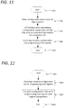
- the arrangement of figure 9 further supports a method of operating an FPGA as described with reference to figure 11 .
- Figure 11 shows a method of operating an FPGA in accordance with an embodiment.
- a method of operating an FPGA comprising the following steps.
- the method starts at step 1101, and proceeds to step 1102 of instructing a multiplexer having an output coupled to a programming flip flop to select an input receiving configuration values implementing a logic function.
- step 1103 instructing a plurality of LUT flip flops to enter an operational configuration wherein each said LUT flip flop receives inputs from the outputs of a plurality of LUTs respectively.
- step 1104 clocking said programming shift register to load a first set of elements thereof with LUT Configuration values belonging to said configuration values implementing said logic function; and clocking said programming shift register to load a second set of elements of said shift register with routing switch configuration belonging to said configuration values implementing said logic function, and terminates at step 1105.
- the method may comprise the additional steps of enabling the output of a first programming shift register from a plurality of programming shift registers, implementing the steps of figure 11 with respect to the first programming shift register, and then repeating these steps for each of said plurality of shift registers.
- the arrangement of figure 9 further supports a method of verifying an FPGA.
- This method may comprise the steps of clocking said first programming shift register to read out a first set of elements thereof with said LUT Configuration values implementing a logic function; and clocking said first programming shift register to read out a second set of elements of said shift register with routing switch Configuration implementing a logic function.
- the method may comprise the additional steps of enabling the output of a first programming shift register from a plurality of programming shift registers, implementing the describe above with respect to the first programming shift register, and then repeating these steps for each of said plurality of shift registers.
- Figure 12 shows a method of verifying an FPGA in accordance with a further embodiment.
- figure 12 is a development of the preceding embodiment.
- a method of operating an FPGA comprising the following steps.
- the method starts at step 1201, and proceeds to step 1202 of clocking said first programming shift register to read out a first set of elements thereof with said LUT Configuration values implementing a logic function and clocking said first programming shift register to read out a second set of elements of said shift register with routing switch Configuration implementing a logic function.
- the method then proceeds to step 1203 of comparing the LUT Configuration implementing a logic function and routing switch Configuration implementing a logic function as read out of said shift register with a LUT Configuration implementing a logic function and routing switch Configuration implementing a logic function as originally read into said shift register, for example in accordance with the method described with reference to figure 11 .
- the method then terminates at step 1204.
- bitstream loaded into the shift register should be identical to that read from the shift register. In a case where the two are found to be identical the operational state of the FPGA, and the corresponding results can be deemed to be verified. In a case where the bitstream loaded into the shift register is not identical to that read from the shift register, some or all of the result must be considered to be unsound.
- the methods and processes described herein may be implemented in whole or part by a computing device. These methods and processes may be implemented by means of computer-application programs or services, an application-programming interface (API), a library, and/or other computer-program product, or any combination of such entities.
- API application-programming interface
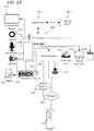
- Figure 13 shows a generic computing system suitable for implementation of embodiments of the invention.
- a system includes a logic device 1301 and a storage device 1302.
- the system may optionally include a display subsystem 1311, input subsystem 1312, 1313, 1315, communication subsystem 1320, and/or other components not shown.
- Logic device 1301 includes one or more physical devices configured to execute instructions.
- the logic device 1301 may be configured to execute instructions that are part of one or more applications, services, programs, routines, libraries, objects, components, data structures, or other logical constructs.
- Such instructions may be implemented to perform a task, implement a data type, transform the state of one or more components, achieve a technical effect, or otherwise arrive at a desired result.
- the logic device 1301 may include one or more processors configured to execute software instructions. Additionally or alternatively, the logic device may include one or more hardware or firmware logic devices configured to execute hardware or firmware instructions. Processors of the logic device may be single-core or multi-core, and the instructions executed thereon may be configured for sequential, parallel, and/or distributed processing. Individual components of the logic device 1301 optionally may be distributed among two or more separate devices, which may be remotely located and/or configured for coordinated processing. Aspects of the logic device 1301 may be virtualized and executed by remotely accessible, networked computing devices configured in a cloud-computing configuration.
- Storage device 1302 includes one or more physical devices configured to hold instructions executable by the logic device to implement the methods and processes described herein. When such methods and processes are implemented, the state of storage 1302 device may be transformed-e.g., to hold different data.
- Storage device 1302 may include removable and/or built-in devices.
- Storage device 1302 may comprise one or more types of storage device including optical memory (e.g., CD, DVD, HD-DVD, Blu-Ray Disc, etc.), semiconductor memory (e.g., RAM, EPROM, EEPROM, etc.), and/or magnetic memory (e.g., hard-disk drive, floppy-disk drive, tape drive, MRAM, etc.), among others.
- Storage device may include volatile, nonvolatile, dynamic, static, read/write, read-only, random-access, sequential-access, location-addressable, file-addressable, and/or content-addressable devices.
- the system may comprise an interface 1303 adapted to support communications between the Logic device 1301 and further system components.
- additional system components may comprise removable and/or built-in extended storage devices.
- Extended storage devices may comprise one or more types of storage device including optical memory 1332 (e.g., CD, DVD, HD-DVD, Blu-Ray Disc, etc.), semiconductor memory 1333 (e.g., RAM, EPROM, EEPROM, FLASH etc.), and/or magnetic memory 1331 (e.g., hard-disk drive, floppy-disk drive, tape drive, MRAM, etc.), among others.
- Such extended storage device may include volatile, nonvolatile, dynamic, static, read/write, read-only, random-access, sequential-access, location-addressable, file-addressable, and/or content-addressable devices.
- storage device includes one or more physical devices, and excludes propagating signals as such.
- aspects of the instructions described herein alternatively may be propagated by a communication medium (e.g., an electromagnetic signal, an optical signal, etc.), as opposed to being stored on a storage device.
- a communication medium e.g., an electromagnetic signal, an optical signal, etc.
- logic device 1301 and storage device 1302 may be integrated together into one or more hardware-logic components.
- Such hardware-logic components may include field-programmable gate arrays (FPGAs), program- and application-specific integrated circuits (PASIC/ASICs), program- and application-specific standard products (PSSP/ASSPs), system-on-a-chip (SOC), and complex programmable logic devices (CPLDs), for example.
- FPGAs field-programmable gate arrays
- PASIC/ASICs program- and application-specific integrated circuits
- PSSP/ASSPs program- and application-specific standard products
- SOC system-on-a-chip
- CPLDs complex programmable logic devices
- program may be used to describe an aspect of computing system implemented to perform a particular function.
- a program may be instantiated via logic device executing machine-readable instructions held by storage device. It will be understood that different modules may be instantiated from the same application, service, code block, object, library, routine, API, function, etc. Likewise, the same program may be instantiated by different applications, services, code blocks, objects, routines, APIs, functions, etc.
- program may encompass individual or groups of executable files, data files, libraries, drivers, scripts, database records, etc.
- system of figure 13 may be used to implement embodiments of the invention.
- a program implementing the steps described with respect to figures 10 , 11 or 12 may be stored in storage device 1302 and executed by logic device 1301.
- the bitstream loaded into the shift register or registers may be generated by the logic device 1301 and/or stored in storage device 1302 or the extended storage devices 1332, 1333 or 1331.
- the bitstream may be loaded into the shift register or registers by the action of the logic device 1301 via the communications interface 1320.
- the bitstream read from the shift register or registers may be retrieved by the action of the logic device 1301 via the communications interface 1320, and/or stored in storage device 1302 or the extended storage devices 1332, 1333 or 1331.
- the Logic device 1301 may retrieve the bitstream loaded to the shift register or registers, and the bitstream read from the shift register or registers in the verification mode, and perform a comparison to determine validity of results.
- the invention may be embodied in the form of a computer program.
- a “service”, as used herein, is an application program executable across multiple user sessions.
- a service may be available to one or more system components, programs, and/or other services.
- a service may run on one or more server-computing devices.
- display subsystem 1311 may be used to present a visual representation of data held by storage device.
- This visual representation may take the form of a graphical user interface (GUI).
- GUI graphical user interface
- the state of display subsystem 1311 may likewise be transformed to visually represent changes in the underlying data.
- Display subsystem 1311 may include one or more display devices utilizing virtually any type of technology. Such display devices may be combined with logic device and/or storage device in a shared enclosure, or such display devices may be peripheral display devices.
- input subsystem may comprise or interface with one or more user-input devices such as a keyboard 1312, mouse 1313, touch screen 1311, or game controller (not shown).
- the input subsystem may comprise or interface with selected natural user input (NUI) componentry.
- NUI natural user input
- Such componentry may be integrated or peripheral, and the transduction and/or processing of input actions may be handled on- or off-board.
- NUI componentry may include a microphone for speech and/or voice recognition; an infrared, color, stereoscopic, and/or depth camera for machine vision and/or gesture recognition; a head tracker, eye tracker, accelerometer, and/or gyroscope for motion detection and/or intent recognition; as well as electric-field sensing componentry for assessing brain activity.
- communication subsystem 1320 may be configured to communicatively couple computing system with one or more other computing devices.
- communication module of may communicatively couple computing device to remote service hosted for example on a remote server 1376 via a network of any size including for example a personal area network, local area network, wide area network, or the internet.
- Communication subsystem may include wired and/or wireless communication devices compatible with one or more different communication protocols.
- the communication subsystem may be configured for communication via a wireless telephone network 1374, or a wired or wireless local- or wide-area network.
- the communication subsystem may allow computing system to send and/or receive messages to and/or from other devices via a network such as the Internet 1375.
- the communications subsystem may additionally support short range inductive communications 1321 with passive devices (NFC, RFID etc).
- configuration values for Lookup tables (LUTs) and programmable routing switches in an FPGA are provided by means of a number of flip flops arranges in a shift register.
- This shift register may receive test values in a factory test mode, and operational configuration values (implementing whatever functionality the client requires of the FPGA) in an operational mode.
- the bitstreams are provided at one end of the shift register, and clocked through until the last flip flop receives its value. Values may also be clocked out at the other end of the shift register to be compared to the initial bitstream in order to identify corruption of stored values e.g. due to radiation exposure.
- a clock gating architecture is proposed for loading data to or reading data from specific selected shift registers.
Landscapes
- Physics & Mathematics (AREA)
- Engineering & Computer Science (AREA)
- General Engineering & Computer Science (AREA)
- Mathematical Physics (AREA)
- General Physics & Mathematics (AREA)
- Computer Hardware Design (AREA)
- Computing Systems (AREA)
- Computer Networks & Wireless Communication (AREA)
- Logic Circuits (AREA)
- Design And Manufacture Of Integrated Circuits (AREA)
- Tests Of Electronic Circuits (AREA)
- Semiconductor Integrated Circuits (AREA)
Priority Applications (1)
| Application Number | Priority Date | Filing Date | Title |
|---|---|---|---|
| EP18192294.9A EP3435545B1 (fr) | 2015-10-15 | 2015-10-15 | Système et procédé de test et de configuration d'un réseau fpga |
Applications Claiming Priority (2)
| Application Number | Priority Date | Filing Date | Title |
|---|---|---|---|
| EP15306641.0A EP3157172B1 (fr) | 2015-10-15 | 2015-10-15 | Système et procédé de test et de configuration d'un réseau fpga |
| EP18192294.9A EP3435545B1 (fr) | 2015-10-15 | 2015-10-15 | Système et procédé de test et de configuration d'un réseau fpga |
Related Parent Applications (2)
| Application Number | Title | Priority Date | Filing Date |
|---|---|---|---|
| EP15306641.0A Division EP3157172B1 (fr) | 2015-10-15 | 2015-10-15 | Système et procédé de test et de configuration d'un réseau fpga |
| EP15306641.0A Division-Into EP3157172B1 (fr) | 2015-10-15 | 2015-10-15 | Système et procédé de test et de configuration d'un réseau fpga |
Publications (3)
| Publication Number | Publication Date |
|---|---|
| EP3435545A1 true EP3435545A1 (fr) | 2019-01-30 |
| EP3435545C0 EP3435545C0 (fr) | 2023-06-07 |
| EP3435545B1 EP3435545B1 (fr) | 2023-06-07 |
Family
ID=54360380
Family Applications (2)
| Application Number | Title | Priority Date | Filing Date |
|---|---|---|---|
| EP15306641.0A Active EP3157172B1 (fr) | 2015-10-15 | 2015-10-15 | Système et procédé de test et de configuration d'un réseau fpga |
| EP18192294.9A Active EP3435545B1 (fr) | 2015-10-15 | 2015-10-15 | Système et procédé de test et de configuration d'un réseau fpga |
Family Applications Before (1)
| Application Number | Title | Priority Date | Filing Date |
|---|---|---|---|
| EP15306641.0A Active EP3157172B1 (fr) | 2015-10-15 | 2015-10-15 | Système et procédé de test et de configuration d'un réseau fpga |
Country Status (11)
| Country | Link |
|---|---|
| US (2) | US10295595B2 (fr) |
| EP (2) | EP3157172B1 (fr) |
| JP (2) | JP2018537871A (fr) |
| KR (1) | KR102564093B1 (fr) |
| CN (3) | CN108028654B (fr) |
| IL (1) | IL253219B (fr) |
| MY (1) | MY184901A (fr) |
| RU (1) | RU2733092C2 (fr) |
| SG (1) | SG11201705319YA (fr) |
| TW (2) | TWI746021B (fr) |
| WO (1) | WO2017063957A1 (fr) |
Cited By (1)
| Publication number | Priority date | Publication date | Assignee | Title |
|---|---|---|---|---|
| CN112580069A (zh) * | 2020-12-05 | 2021-03-30 | 西安翔腾微电子科技有限公司 | 一种主机在线加载配置表权限获取的方法 |
Families Citing this family (53)
| Publication number | Priority date | Publication date | Assignee | Title |
|---|---|---|---|---|
| US11625523B2 (en) | 2016-12-14 | 2023-04-11 | iCometrue Company Ltd. | Logic drive based on standard commodity FPGA IC chips |
| TW202537391A (zh) | 2016-12-14 | 2025-09-16 | 成真股份有限公司 | 標準大宗商品化現場可編程邏輯閘陣列(fpga)積體電路晶片組成之邏輯驅動器 |
| US10963001B1 (en) | 2017-04-18 | 2021-03-30 | Amazon Technologies, Inc. | Client configurable hardware logic and corresponding hardware clock metadata |
| US10447274B2 (en) | 2017-07-11 | 2019-10-15 | iCometrue Company Ltd. | Logic drive based on standard commodity FPGA IC chips using non-volatile memory cells |
| US10957679B2 (en) | 2017-08-08 | 2021-03-23 | iCometrue Company Ltd. | Logic drive based on standardized commodity programmable logic semiconductor IC chips |
| US10630296B2 (en) | 2017-09-12 | 2020-04-21 | iCometrue Company Ltd. | Logic drive with brain-like elasticity and integrality based on standard commodity FPGA IC chips using non-volatile memory cells |
| WO2019129389A1 (fr) * | 2017-12-26 | 2019-07-04 | Silicon Mobility Sas | Unité logique flexible conçue pour une commutation de tâches en temps réel |
| US10608642B2 (en) | 2018-02-01 | 2020-03-31 | iCometrue Company Ltd. | Logic drive using standard commodity programmable logic IC chips comprising non-volatile radom access memory cells |
| US10623000B2 (en) | 2018-02-14 | 2020-04-14 | iCometrue Company Ltd. | Logic drive using standard commodity programmable logic IC chips |
| US10707873B2 (en) * | 2018-03-21 | 2020-07-07 | University Of Southern California | Superconducting magnetic field programmable gate array |
| US10608638B2 (en) | 2018-05-24 | 2020-03-31 | iCometrue Company Ltd. | Logic drive using standard commodity programmable logic IC chips |
| US12476637B2 (en) | 2018-05-24 | 2025-11-18 | iCometrue Company Ltd. | Logic drive using standard commodity programmable logic IC chips |
| US10892011B2 (en) | 2018-09-11 | 2021-01-12 | iCometrue Company Ltd. | Logic drive using standard commodity programmable logic IC chips comprising non-volatile random access memory cells |
| US11309334B2 (en) | 2018-09-11 | 2022-04-19 | iCometrue Company Ltd. | Logic drive using standard commodity programmable logic IC chips comprising non-volatile random access memory cells |
| US10937762B2 (en) | 2018-10-04 | 2021-03-02 | iCometrue Company Ltd. | Logic drive based on multichip package using interconnection bridge |
| US11616046B2 (en) | 2018-11-02 | 2023-03-28 | iCometrue Company Ltd. | Logic drive based on chip scale package comprising standardized commodity programmable logic IC chip and memory IC chip |
| US11211334B2 (en) | 2018-11-18 | 2021-12-28 | iCometrue Company Ltd. | Logic drive based on chip scale package comprising standardized commodity programmable logic IC chip and memory IC chip |
| US10831507B2 (en) | 2018-11-21 | 2020-11-10 | SambaNova Systems, Inc. | Configuration load of a reconfigurable data processor |
| US11188497B2 (en) | 2018-11-21 | 2021-11-30 | SambaNova Systems, Inc. | Configuration unload of a reconfigurable data processor |
| CN109445876B (zh) * | 2018-12-12 | 2023-04-11 | 北京时代奥视科技有限公司 | Lut数据加载的方法及监视器 |
| EP3667529B1 (fr) | 2018-12-14 | 2024-02-28 | Siemens Aktiengesellschaft | Procédé et dispositif d'authentification d'une configuration du réseau prédiffusé programmable par l'utilisateur fpga |
| US10698853B1 (en) | 2019-01-03 | 2020-06-30 | SambaNova Systems, Inc. | Virtualization of a reconfigurable data processor |
| US10768899B2 (en) | 2019-01-29 | 2020-09-08 | SambaNova Systems, Inc. | Matrix normal/transpose read and a reconfigurable data processor including same |
| CN109857024B (zh) * | 2019-02-01 | 2021-11-12 | 京微齐力(北京)科技有限公司 | 人工智能模块的单元性能测试方法和系统芯片 |
| US11386038B2 (en) | 2019-05-09 | 2022-07-12 | SambaNova Systems, Inc. | Control flow barrier and reconfigurable data processor |
| US10985154B2 (en) | 2019-07-02 | 2021-04-20 | iCometrue Company Ltd. | Logic drive based on multichip package comprising standard commodity FPGA IC chip with cryptography circuits |
| US11227838B2 (en) | 2019-07-02 | 2022-01-18 | iCometrue Company Ltd. | Logic drive based on multichip package comprising standard commodity FPGA IC chip with cooperating or supporting circuits |
| US11055141B2 (en) | 2019-07-08 | 2021-07-06 | SambaNova Systems, Inc. | Quiesce reconfigurable data processor |
| US11887930B2 (en) | 2019-08-05 | 2024-01-30 | iCometrue Company Ltd. | Vertical interconnect elevator based on through silicon vias |
| JP7037528B2 (ja) * | 2019-09-12 | 2022-03-16 | 株式会社東芝 | 集積回路およびそのテスト方法ならびに電子機器 |
| US11637056B2 (en) | 2019-09-20 | 2023-04-25 | iCometrue Company Ltd. | 3D chip package based on through-silicon-via interconnection elevator |
| CN111175637B (zh) * | 2020-01-09 | 2022-02-15 | 深圳市正宇兴电子有限公司 | 一种基于功能测试的光学soc芯片测试方法及系统 |
| US11037069B1 (en) * | 2020-01-17 | 2021-06-15 | Tegze P. Haraszti | Method for creating gates and circuits for greatly improved computing apparatus by using symbol transformer |
| US11600526B2 (en) | 2020-01-22 | 2023-03-07 | iCometrue Company Ltd. | Chip package based on through-silicon-via connector and silicon interconnection bridge |
| TWI734420B (zh) * | 2020-03-18 | 2021-07-21 | 國立成功大學 | 具掃描鍊架構與邏輯單元矩陣之測試晶片架構及其診斷方法 |
| US11809908B2 (en) | 2020-07-07 | 2023-11-07 | SambaNova Systems, Inc. | Runtime virtualization of reconfigurable data flow resources |
| US11782729B2 (en) | 2020-08-18 | 2023-10-10 | SambaNova Systems, Inc. | Runtime patching of configuration files |
| CN112147492B (zh) * | 2020-10-13 | 2022-03-22 | 无锡中微亿芯有限公司 | 一种查找表的新型可测试性结构 |
| CN114442736B (zh) * | 2020-11-02 | 2023-09-05 | 芯启源(上海)半导体科技有限公司 | 基于动态配置接口的时钟配置器、fpga系统 |
| TW202240808A (zh) | 2021-01-08 | 2022-10-16 | 成真股份有限公司 | 使用於積體電路晶片封裝結構中的微型熱導管 |
| CN112861455B (zh) * | 2021-03-12 | 2022-05-17 | 上海先基半导体科技有限公司 | Fpga建模验证系统及方法 |
| CN113098597A (zh) * | 2021-03-31 | 2021-07-09 | 北京百度网讯科技有限公司 | 光保护装置以及光功率检测的方法 |
| US12176278B2 (en) | 2021-05-30 | 2024-12-24 | iCometrue Company Ltd. | 3D chip package based on vertical-through-via connector |
| US11556494B1 (en) | 2021-07-16 | 2023-01-17 | SambaNova Systems, Inc. | Defect repair for a reconfigurable data processor for homogeneous subarrays |
| US11327771B1 (en) | 2021-07-16 | 2022-05-10 | SambaNova Systems, Inc. | Defect repair circuits for a reconfigurable data processor |
| US11409540B1 (en) | 2021-07-16 | 2022-08-09 | SambaNova Systems, Inc. | Routing circuits for defect repair for a reconfigurable data processor |
| CN113505096B (zh) * | 2021-08-05 | 2022-10-18 | 北京极光星通科技有限公司 | 星载激光通信终端及其功耗控制方法 |
| US11736107B2 (en) * | 2021-08-19 | 2023-08-22 | Wuxi Esiontech Co., Ltd. | Field-programmable gate array (FPGA) for using configuration shift chain to implement multi-bitstream function |
| US20230187365A1 (en) | 2021-09-24 | 2023-06-15 | iCometrue Company Ltd. | Field Programmable Multichip Package Based on Field-Programmable-Gate-Array (FPGA) Integrated-Circuit (IC) Chip |
| US12268012B2 (en) | 2021-09-24 | 2025-04-01 | iCometrue Company Ltd. | Multi-output look-up table (LUT) for use in coarse-grained field-programmable-gate-array (FPGA) integrated-circuit (IC) chip |
| US11487694B1 (en) | 2021-12-17 | 2022-11-01 | SambaNova Systems, Inc. | Hot-plug events in a pool of reconfigurable data flow resources |
| CN116450425B (zh) * | 2022-11-24 | 2025-04-15 | 北京时代民芯科技有限公司 | 一种抗辐照FPGA内嵌PCIExpress IP核的测试电路和方法 |
| CN120405391B (zh) * | 2025-07-07 | 2025-10-03 | 珠海硅芯科技有限公司 | 基于eFPGA电路的集成电路的测试方法及装置 |
Citations (8)
| Publication number | Priority date | Publication date | Assignee | Title |
|---|---|---|---|---|
| US5027355A (en) | 1989-04-14 | 1991-06-25 | Control Data Corporation | Logic circuit and design method for improved testability |
| US5432441A (en) | 1986-09-19 | 1995-07-11 | Actel Corporation | Testability architecture and techniques for programmable interconnect architecture |
| US5675589A (en) | 1994-04-01 | 1997-10-07 | Xilinx, Inc. | Programmable scan chain testing structure and method |
| US6021513A (en) | 1995-12-12 | 2000-02-01 | International Business Machines Corporation | Testable programmable gate array and associated LSSD/deterministic test methodology |
| US20080133988A1 (en) * | 2006-11-30 | 2008-06-05 | Quicklogic Corporation | FPGA Programming Structure for ATPG Test Coverage |
| US7463056B1 (en) | 2005-12-12 | 2008-12-09 | Xilinx, Inc. | Writeable shift register lookup table in FPGA with SRAM memory cells in lookup table reprogrammed by writing after initial configuration |
| US8040152B1 (en) * | 2010-02-02 | 2011-10-18 | Lattice Semiconductor Corporation | Separate configuration of I/O cells and logic core in a programmable logic device |
| WO2012123243A1 (fr) | 2011-03-11 | 2012-09-20 | S.A.S Adicsys | Systeme mono-puce comprenant un coeur programmable synthetisable et un procede de fabrication d'un tel systeme |
Family Cites Families (40)
| Publication number | Priority date | Publication date | Assignee | Title |
|---|---|---|---|---|
| SU1578715A1 (ru) * | 1988-01-07 | 1990-07-15 | Предприятие П/Я Р-6120 | Тестопригодное цифровое устройство |
| US5212652A (en) * | 1989-08-15 | 1993-05-18 | Advanced Micro Devices, Inc. | Programmable gate array with improved interconnect structure |
| JPH03139863A (ja) * | 1989-10-25 | 1991-06-14 | Hitachi Ltd | 半導体集積回路 |
| JP2564044B2 (ja) * | 1991-02-27 | 1996-12-18 | 株式会社東芝 | プログラマブル論理回路 |
| JPH06148274A (ja) * | 1992-11-02 | 1994-05-27 | Kawasaki Steel Corp | 集積回路 |
| KR0148141B1 (ko) * | 1993-07-31 | 1998-09-15 | 김광호 | 블랭킹레벨조정방법 및 그 장치 |
| US5654650A (en) * | 1995-12-11 | 1997-08-05 | Hewlett-Packard Company | High throughput FPGA control interface |
| US5760602A (en) * | 1996-01-17 | 1998-06-02 | Hewlett-Packard Company | Time multiplexing a plurality of configuration settings of a programmable switch element in a FPGA |
| US5889413A (en) * | 1996-11-22 | 1999-03-30 | Xilinx, Inc. | Lookup tables which double as shift registers |
| US6011406A (en) * | 1997-10-28 | 2000-01-04 | Altera Corporation | Ultra-fast configuration mode for a programmable logic device |
| US6347387B1 (en) * | 1998-10-09 | 2002-02-12 | Agere Systems Guardian Corp. | Test circuits for testing inter-device FPGA links including a shift register configured from FPGA elements to form a shift block through said inter-device FPGA links |
| US6215327B1 (en) * | 1999-09-01 | 2001-04-10 | The United States Of America As Represented By The Secretary Of The Air Force | Molecular field programmable gate array |
| JP2001298357A (ja) * | 2000-04-13 | 2001-10-26 | Seiko Epson Corp | フィールド・プログラマブル・ゲートアレイ |
| US6470485B1 (en) * | 2000-10-18 | 2002-10-22 | Lattice Semiconductor Corporation | Scalable and parallel processing methods and structures for testing configurable interconnect network in FPGA device |
| US6384627B1 (en) * | 2001-02-16 | 2002-05-07 | Xilinx, Inc. | Logic block used as dynamically configurable logic function |
| JP3938308B2 (ja) * | 2001-12-28 | 2007-06-27 | 富士通株式会社 | プログラマブル論理デバイス |
| US7028281B1 (en) * | 2002-07-12 | 2006-04-11 | Lattice Semiconductor Corporation | FPGA with register-intensive architecture |
| US7111214B1 (en) * | 2002-10-09 | 2006-09-19 | Xilinx, Inc. | Circuits and methods for testing programmable logic devices using lookup tables and carry chains |
| DE102005023118B3 (de) * | 2005-05-19 | 2006-12-21 | Infineon Technologies Ag | Schaltungsanordnung zum Zuführen von Konfigurationsdaten in FPGA-Einrichtungen |
| US7804719B1 (en) * | 2005-06-14 | 2010-09-28 | Xilinx, Inc. | Programmable logic block having reduced output delay during RAM write processes when programmed to function in RAM mode |
| US8195103B2 (en) * | 2006-02-15 | 2012-06-05 | Texas Instruments Incorporated | Linearization of a transmit amplifier |
| JP5035239B2 (ja) * | 2006-03-15 | 2012-09-26 | 日本電気株式会社 | 再構成可能デバイスのテストシステム及びその方法並びにそれに用いる再構成可能デバイス |
| US7362135B1 (en) * | 2006-10-04 | 2008-04-22 | Hyun-Taek Chang | Apparatus and method for clock skew adjustment in a programmable logic fabric |
| US7925940B2 (en) * | 2007-10-17 | 2011-04-12 | Synopsys, Inc. | Enhancing speed of simulation of an IC design while testing scan circuitry |
| US7809521B1 (en) * | 2008-02-29 | 2010-10-05 | The United States Of America As Represented By The Administrator Of The National Aeronautics And Space Administration | Precise delay measurement through combinatorial logic |
| US20100124272A1 (en) * | 2008-11-19 | 2010-05-20 | Gene Fein | Coded pulse data transmission using a look-up table |
| CN101510775B (zh) * | 2009-03-20 | 2012-01-18 | 复旦大学 | 可进化数字电路及其进化方法 |
| CN101923440B (zh) * | 2009-06-15 | 2011-12-14 | 杭州中科微电子有限公司 | 一种高速异步数据采集系统 |
| US7859292B1 (en) * | 2009-07-14 | 2010-12-28 | United States Of America As Represented By The Administrator Of The National Aeronautics And Space Administration | Methods and circuitry for reconfigurable SEU/SET tolerance |
| IT1398937B1 (it) * | 2010-02-17 | 2013-03-28 | St Microelectronics Srl | Metodo per eseguire un testing elettrico di dispositivi elettronici |
| KR101681736B1 (ko) * | 2010-05-14 | 2016-12-02 | 삼성전자주식회사 | 입출력 래퍼들을 갖는 반도체 장치 |
| DE112012003335T5 (de) * | 2011-08-12 | 2014-04-30 | Denso Corp. | Integrierte Schaltung |
| KR20130066267A (ko) * | 2011-12-12 | 2013-06-20 | 한국전자통신연구원 | 필드 프로그래머블 게이트 어레이의 스위치 블록 회로 |
| US9121892B2 (en) * | 2012-08-13 | 2015-09-01 | Analog Devices Global | Semiconductor circuit and methodology for in-system scan testing |
| CN103914580B (zh) * | 2012-12-31 | 2017-07-11 | 复旦大学 | 一种用于fpga电路位流仿真的方法 |
| CN103632726B (zh) * | 2013-01-31 | 2017-02-08 | 中国科学院电子学研究所 | 一种基于可编程基本逻辑单元的数据移位寄存电路 |
| CN103236836B (zh) * | 2013-04-10 | 2016-03-16 | 中国科学院微电子研究所 | 具有mux模式的lut结构及与其相配套的eda优化方法 |
| JP6426437B2 (ja) * | 2013-11-22 | 2018-11-21 | 株式会社半導体エネルギー研究所 | 半導体装置 |
| JP6541376B2 (ja) * | 2014-03-13 | 2019-07-10 | 株式会社半導体エネルギー研究所 | プログラマブルロジックデバイスの動作方法 |
| US9576625B1 (en) * | 2015-10-08 | 2017-02-21 | Altera Corporation | Register initialization using multi-pass configuration |
-
2015
- 2015-10-15 EP EP15306641.0A patent/EP3157172B1/fr active Active
- 2015-10-15 EP EP18192294.9A patent/EP3435545B1/fr active Active
-
2016
- 2016-10-07 JP JP2017536024A patent/JP2018537871A/ja active Pending
- 2016-10-07 MY MYPI2017001004A patent/MY184901A/en unknown
- 2016-10-07 CN CN201680007693.4A patent/CN108028654B/zh active Active
- 2016-10-07 WO PCT/EP2016/074076 patent/WO2017063957A1/fr not_active Ceased
- 2016-10-07 RU RU2017129272A patent/RU2733092C2/ru active
- 2016-10-07 CN CN202210218457.4A patent/CN114553215B/zh active Active
- 2016-10-07 SG SG11201705319YA patent/SG11201705319YA/en unknown
- 2016-10-07 US US15/540,997 patent/US10295595B2/en active Active
- 2016-10-07 CN CN202211257072.5A patent/CN115542139A/zh active Pending
- 2016-10-07 KR KR1020177022639A patent/KR102564093B1/ko active Active
- 2016-10-13 TW TW109120881A patent/TWI746021B/zh active
- 2016-10-13 TW TW105133080A patent/TWI717399B/zh active
-
2017
- 2017-06-28 IL IL253219A patent/IL253219B/en unknown
-
2019
- 2019-04-04 US US16/375,339 patent/US10746796B2/en active Active
-
2021
- 2021-04-30 JP JP2021077157A patent/JP7286706B2/ja active Active
Patent Citations (9)
| Publication number | Priority date | Publication date | Assignee | Title |
|---|---|---|---|---|
| US5432441A (en) | 1986-09-19 | 1995-07-11 | Actel Corporation | Testability architecture and techniques for programmable interconnect architecture |
| US5027355A (en) | 1989-04-14 | 1991-06-25 | Control Data Corporation | Logic circuit and design method for improved testability |
| US5675589A (en) | 1994-04-01 | 1997-10-07 | Xilinx, Inc. | Programmable scan chain testing structure and method |
| US6021513A (en) | 1995-12-12 | 2000-02-01 | International Business Machines Corporation | Testable programmable gate array and associated LSSD/deterministic test methodology |
| US7463056B1 (en) | 2005-12-12 | 2008-12-09 | Xilinx, Inc. | Writeable shift register lookup table in FPGA with SRAM memory cells in lookup table reprogrammed by writing after initial configuration |
| US20080133988A1 (en) * | 2006-11-30 | 2008-06-05 | Quicklogic Corporation | FPGA Programming Structure for ATPG Test Coverage |
| US8091001B2 (en) | 2006-11-30 | 2012-01-03 | Quicklogic Corporation | FPGA programming structure for ATPG test coverage |
| US8040152B1 (en) * | 2010-02-02 | 2011-10-18 | Lattice Semiconductor Corporation | Separate configuration of I/O cells and logic core in a programmable logic device |
| WO2012123243A1 (fr) | 2011-03-11 | 2012-09-20 | S.A.S Adicsys | Systeme mono-puce comprenant un coeur programmable synthetisable et un procede de fabrication d'un tel systeme |
Non-Patent Citations (1)
| Title |
|---|
| VICTOR OLUBUNMI AKEN'OVA: "Bridging the Gap between Soft and Hard eFPGA Design" |
Cited By (2)
| Publication number | Priority date | Publication date | Assignee | Title |
|---|---|---|---|---|
| CN112580069A (zh) * | 2020-12-05 | 2021-03-30 | 西安翔腾微电子科技有限公司 | 一种主机在线加载配置表权限获取的方法 |
| CN112580069B (zh) * | 2020-12-05 | 2023-04-07 | 西安翔腾微电子科技有限公司 | 一种主机在线加载配置表权限获取的方法 |
Also Published As
| Publication number | Publication date |
|---|---|
| US20190227120A1 (en) | 2019-07-25 |
| RU2733092C2 (ru) | 2020-09-29 |
| RU2017129272A3 (fr) | 2020-04-21 |
| TW202040941A (zh) | 2020-11-01 |
| CN115542139A (zh) | 2022-12-30 |
| EP3157172A1 (fr) | 2017-04-19 |
| RU2017129272A (ru) | 2019-02-18 |
| TW201729542A (zh) | 2017-08-16 |
| TWI746021B (zh) | 2021-11-11 |
| US10746796B2 (en) | 2020-08-18 |
| EP3435545C0 (fr) | 2023-06-07 |
| MY184901A (en) | 2021-04-30 |
| JP2021145339A (ja) | 2021-09-24 |
| IL253219B (en) | 2022-02-01 |
| US10295595B2 (en) | 2019-05-21 |
| CN114553215A (zh) | 2022-05-27 |
| CN108028654B (zh) | 2023-04-04 |
| US20180275193A1 (en) | 2018-09-27 |
| CN114553215B (zh) | 2026-03-17 |
| SG11201705319YA (en) | 2017-07-28 |
| JP2018537871A (ja) | 2018-12-20 |
| CN108028654A (zh) | 2018-05-11 |
| TWI717399B (zh) | 2021-02-01 |
| CA2973530A1 (fr) | 2017-04-20 |
| EP3435545B1 (fr) | 2023-06-07 |
| EP3157172B1 (fr) | 2018-11-28 |
| JP7286706B2 (ja) | 2023-06-05 |
| WO2017063957A1 (fr) | 2017-04-20 |
| KR20180068895A (ko) | 2018-06-22 |
| KR102564093B1 (ko) | 2023-08-04 |
| IL253219A0 (en) | 2017-08-31 |
Similar Documents
| Publication | Publication Date | Title |
|---|---|---|
| US10746796B2 (en) | System and method for testing and configuration of an FPGA | |
| US9739833B2 (en) | Scan chain for memory sequential test | |
| US9495492B1 (en) | Implementing synchronous triggers for waveform capture in an FPGA prototyping system | |
| US20080272805A1 (en) | Method and apparatus for boundary scan programming of memory devices | |
| EP3355196A1 (fr) | Fpga et procédé de fonctionnement | |
| US7739093B2 (en) | Method of visualization in processor based emulation system | |
| CN107145465B (zh) | 串行外设接口spi的传输控制方法、装置及系统 | |
| JP6257044B2 (ja) | システムオンチップ内のメモリ回路および論理回路のレイアウト | |
| US6059836A (en) | Logic circuit emulator | |
| CA2973530C (fr) | Systeme et procede d'essai et de configuration d'un reseau prediffuse programmable par l'utilisateur | |
| US7395197B2 (en) | Verification method and system for logic circuit | |
| HK40003241A (en) | System and method for testing and configuration of an fpga | |
| HK1236287A (en) | System and method for testing and configuration of an fpga | |
| HK1236287A1 (en) | System and method for testing and configuration of an fpga | |
| HK1236287B (en) | System and method for testing and configuration of an fpga | |
| EP3376669A1 (fr) | Fpga et procédé de programmation fpga | |
| HK40079336A (en) | System and method for testing and configuration of an fpga | |
| US7827023B2 (en) | Method and apparatus for increasing the efficiency of an emulation engine | |
| US20250061958A1 (en) | Logic device and system and methods for definition and configuration of a logic device | |
| US9627017B1 (en) | RAM at speed flexible timing and setup control | |
| Radoslaw Rybaniec | FPGA FIRMWARE FRAMEWORK FOR MTCA. 4 AMC MODULES |
Legal Events
| Date | Code | Title | Description |
|---|---|---|---|
| PUAI | Public reference made under article 153(3) epc to a published international application that has entered the european phase |
Free format text: ORIGINAL CODE: 0009012 |
|
| STAA | Information on the status of an ep patent application or granted ep patent |
Free format text: STATUS: THE APPLICATION HAS BEEN PUBLISHED |
|
| AC | Divisional application: reference to earlier application |
Ref document number: 3157172 Country of ref document: EP Kind code of ref document: P |
|
| AK | Designated contracting states |
Kind code of ref document: A1 Designated state(s): AL AT BE BG CH CY CZ DE DK EE ES FI FR GB GR HR HU IE IS IT LI LT LU LV MC MK MT NL NO PL PT RO RS SE SI SK SM TR |
|
| STAA | Information on the status of an ep patent application or granted ep patent |
Free format text: STATUS: REQUEST FOR EXAMINATION WAS MADE |
|
| 17P | Request for examination filed |
Effective date: 20190723 |
|
| RBV | Designated contracting states (corrected) |
Designated state(s): AL AT BE BG CH CY CZ DE DK EE ES FI FR GB GR HR HU IE IS IT LI LT LU LV MC MK MT NL NO PL PT RO RS SE SI SK SM TR |
|
| REG | Reference to a national code |
Ref country code: HK Ref legal event code: DE Ref document number: 40003241 Country of ref document: HK |
|
| STAA | Information on the status of an ep patent application or granted ep patent |
Free format text: STATUS: EXAMINATION IS IN PROGRESS |
|
| 17Q | First examination report despatched |
Effective date: 20210507 |
|
| GRAP | Despatch of communication of intention to grant a patent |
Free format text: ORIGINAL CODE: EPIDOSNIGR1 |
|
| STAA | Information on the status of an ep patent application or granted ep patent |
Free format text: STATUS: GRANT OF PATENT IS INTENDED |
|
| INTG | Intention to grant announced |
Effective date: 20221206 |
|
| GRAS | Grant fee paid |
Free format text: ORIGINAL CODE: EPIDOSNIGR3 |
|
| GRAA | (expected) grant |
Free format text: ORIGINAL CODE: 0009210 |
|
| STAA | Information on the status of an ep patent application or granted ep patent |
Free format text: STATUS: THE PATENT HAS BEEN GRANTED |
|
| AC | Divisional application: reference to earlier application |
Ref document number: 3157172 Country of ref document: EP Kind code of ref document: P |
|
| AK | Designated contracting states |
Kind code of ref document: B1 Designated state(s): AL AT BE BG CH CY CZ DE DK EE ES FI FR GB GR HR HU IE IS IT LI LT LU LV MC MK MT NL NO PL PT RO RS SE SI SK SM TR |
|
| REG | Reference to a national code |
Ref country code: GB Ref legal event code: FG4D |
|
| REG | Reference to a national code |
Ref country code: CH Ref legal event code: EP Ref country code: AT Ref legal event code: REF Ref document number: 1577888 Country of ref document: AT Kind code of ref document: T Effective date: 20230615 |
|
| REG | Reference to a national code |
Ref country code: DE Ref legal event code: R096 Ref document number: 602015084089 Country of ref document: DE |
|
| U01 | Request for unitary effect filed |
Effective date: 20230623 |
|
| RAP4 | Party data changed (patent owner data changed or rights of a patent transferred) |
Owner name: MENTA |
|
| U07 | Unitary effect registered |
Designated state(s): AT BE BG DE DK EE FI FR IT LT LU LV MT NL PT SE SI Effective date: 20230717 |
|
| REG | Reference to a national code |
Ref country code: LT Ref legal event code: MG9D |
|
| U20 | Renewal fee for the european patent with unitary effect paid |
Year of fee payment: 9 Effective date: 20230921 |
|
| PG25 | Lapsed in a contracting state [announced via postgrant information from national office to epo] |
Ref country code: NO Free format text: LAPSE BECAUSE OF FAILURE TO SUBMIT A TRANSLATION OF THE DESCRIPTION OR TO PAY THE FEE WITHIN THE PRESCRIBED TIME-LIMIT Effective date: 20230907 Ref country code: ES Free format text: LAPSE BECAUSE OF FAILURE TO SUBMIT A TRANSLATION OF THE DESCRIPTION OR TO PAY THE FEE WITHIN THE PRESCRIBED TIME-LIMIT Effective date: 20230607 |
|
| PG25 | Lapsed in a contracting state [announced via postgrant information from national office to epo] |
Ref country code: RS Free format text: LAPSE BECAUSE OF FAILURE TO SUBMIT A TRANSLATION OF THE DESCRIPTION OR TO PAY THE FEE WITHIN THE PRESCRIBED TIME-LIMIT Effective date: 20230607 Ref country code: HR Free format text: LAPSE BECAUSE OF FAILURE TO SUBMIT A TRANSLATION OF THE DESCRIPTION OR TO PAY THE FEE WITHIN THE PRESCRIBED TIME-LIMIT Effective date: 20230607 Ref country code: GR Free format text: LAPSE BECAUSE OF FAILURE TO SUBMIT A TRANSLATION OF THE DESCRIPTION OR TO PAY THE FEE WITHIN THE PRESCRIBED TIME-LIMIT Effective date: 20230908 |
|
| PG25 | Lapsed in a contracting state [announced via postgrant information from national office to epo] |
Ref country code: SK Free format text: LAPSE BECAUSE OF FAILURE TO SUBMIT A TRANSLATION OF THE DESCRIPTION OR TO PAY THE FEE WITHIN THE PRESCRIBED TIME-LIMIT Effective date: 20230607 |
|
| PG25 | Lapsed in a contracting state [announced via postgrant information from national office to epo] |
Ref country code: IS Free format text: LAPSE BECAUSE OF FAILURE TO SUBMIT A TRANSLATION OF THE DESCRIPTION OR TO PAY THE FEE WITHIN THE PRESCRIBED TIME-LIMIT Effective date: 20231007 |
|
| PG25 | Lapsed in a contracting state [announced via postgrant information from national office to epo] |
Ref country code: SM Free format text: LAPSE BECAUSE OF FAILURE TO SUBMIT A TRANSLATION OF THE DESCRIPTION OR TO PAY THE FEE WITHIN THE PRESCRIBED TIME-LIMIT Effective date: 20230607 Ref country code: SK Free format text: LAPSE BECAUSE OF FAILURE TO SUBMIT A TRANSLATION OF THE DESCRIPTION OR TO PAY THE FEE WITHIN THE PRESCRIBED TIME-LIMIT Effective date: 20230607 Ref country code: RO Free format text: LAPSE BECAUSE OF FAILURE TO SUBMIT A TRANSLATION OF THE DESCRIPTION OR TO PAY THE FEE WITHIN THE PRESCRIBED TIME-LIMIT Effective date: 20230607 Ref country code: IS Free format text: LAPSE BECAUSE OF FAILURE TO SUBMIT A TRANSLATION OF THE DESCRIPTION OR TO PAY THE FEE WITHIN THE PRESCRIBED TIME-LIMIT Effective date: 20231007 Ref country code: CZ Free format text: LAPSE BECAUSE OF FAILURE TO SUBMIT A TRANSLATION OF THE DESCRIPTION OR TO PAY THE FEE WITHIN THE PRESCRIBED TIME-LIMIT Effective date: 20230607 |
|
| PG25 | Lapsed in a contracting state [announced via postgrant information from national office to epo] |
Ref country code: PL Free format text: LAPSE BECAUSE OF FAILURE TO SUBMIT A TRANSLATION OF THE DESCRIPTION OR TO PAY THE FEE WITHIN THE PRESCRIBED TIME-LIMIT Effective date: 20230607 |
|
| REG | Reference to a national code |
Ref country code: DE Ref legal event code: R097 Ref document number: 602015084089 Country of ref document: DE |
|
| PLBE | No opposition filed within time limit |
Free format text: ORIGINAL CODE: 0009261 |
|
| STAA | Information on the status of an ep patent application or granted ep patent |
Free format text: STATUS: NO OPPOSITION FILED WITHIN TIME LIMIT |
|
| 26N | No opposition filed |
Effective date: 20240308 |
|
| PG25 | Lapsed in a contracting state [announced via postgrant information from national office to epo] |
Ref country code: MC Free format text: LAPSE BECAUSE OF FAILURE TO SUBMIT A TRANSLATION OF THE DESCRIPTION OR TO PAY THE FEE WITHIN THE PRESCRIBED TIME-LIMIT Effective date: 20230607 |
|
| REG | Reference to a national code |
Ref country code: CH Ref legal event code: PL |
|
| PG25 | Lapsed in a contracting state [announced via postgrant information from national office to epo] |
Ref country code: CH Free format text: LAPSE BECAUSE OF NON-PAYMENT OF DUE FEES Effective date: 20231031 |
|
| PG25 | Lapsed in a contracting state [announced via postgrant information from national office to epo] |
Ref country code: CH Free format text: LAPSE BECAUSE OF NON-PAYMENT OF DUE FEES Effective date: 20231031 |
|
| PG25 | Lapsed in a contracting state [announced via postgrant information from national office to epo] |
Ref country code: IE Free format text: LAPSE BECAUSE OF NON-PAYMENT OF DUE FEES Effective date: 20231015 |
|
| U20 | Renewal fee for the european patent with unitary effect paid |
Year of fee payment: 10 Effective date: 20240920 |
|
| PG25 | Lapsed in a contracting state [announced via postgrant information from national office to epo] |
Ref country code: IE Free format text: LAPSE BECAUSE OF NON-PAYMENT OF DUE FEES Effective date: 20231015 |
|
| PG25 | Lapsed in a contracting state [announced via postgrant information from national office to epo] |
Ref country code: CY Free format text: LAPSE BECAUSE OF FAILURE TO SUBMIT A TRANSLATION OF THE DESCRIPTION OR TO PAY THE FEE WITHIN THE PRESCRIBED TIME-LIMIT; INVALID AB INITIO Effective date: 20151015 |
|
| PG25 | Lapsed in a contracting state [announced via postgrant information from national office to epo] |
Ref country code: HU Free format text: LAPSE BECAUSE OF FAILURE TO SUBMIT A TRANSLATION OF THE DESCRIPTION OR TO PAY THE FEE WITHIN THE PRESCRIBED TIME-LIMIT; INVALID AB INITIO Effective date: 20151015 |
|
| PGFP | Annual fee paid to national office [announced via postgrant information from national office to epo] |
Ref country code: GB Payment date: 20250918 Year of fee payment: 11 |
|
| U20 | Renewal fee for the european patent with unitary effect paid |
Year of fee payment: 11 Effective date: 20250922 |
|
| PG25 | Lapsed in a contracting state [announced via postgrant information from national office to epo] |
Ref country code: TR Free format text: LAPSE BECAUSE OF FAILURE TO SUBMIT A TRANSLATION OF THE DESCRIPTION OR TO PAY THE FEE WITHIN THE PRESCRIBED TIME-LIMIT Effective date: 20230607 |