EP3441506A1 - SUBSTRAT DE SiC POLYCRISTALLIN ET PROCÉDÉ POUR SA FABRICATION - Google Patents
SUBSTRAT DE SiC POLYCRISTALLIN ET PROCÉDÉ POUR SA FABRICATION Download PDFInfo
- Publication number
- EP3441506A1 EP3441506A1 EP17779177.9A EP17779177A EP3441506A1 EP 3441506 A1 EP3441506 A1 EP 3441506A1 EP 17779177 A EP17779177 A EP 17779177A EP 3441506 A1 EP3441506 A1 EP 3441506A1
- Authority
- EP
- European Patent Office
- Prior art keywords
- polycrystalline sic
- base material
- substrate
- sic
- polycrystalline
- Prior art date
- Legal status (The legal status is an assumption and is not a legal conclusion. Google has not performed a legal analysis and makes no representation as to the accuracy of the status listed.)
- Pending
Links
Images





Classifications
-
- C—CHEMISTRY; METALLURGY
- C30—CRYSTAL GROWTH
- C30B—SINGLE-CRYSTAL GROWTH; UNIDIRECTIONAL SOLIDIFICATION OF EUTECTIC MATERIAL OR UNIDIRECTIONAL DEMIXING OF EUTECTOID MATERIAL; REFINING BY ZONE-MELTING OF MATERIAL; PRODUCTION OF A HOMOGENEOUS POLYCRYSTALLINE MATERIAL WITH DEFINED STRUCTURE; SINGLE CRYSTALS OR HOMOGENEOUS POLYCRYSTALLINE MATERIAL WITH DEFINED STRUCTURE; AFTER-TREATMENT OF SINGLE CRYSTALS OR A HOMOGENEOUS POLYCRYSTALLINE MATERIAL WITH DEFINED STRUCTURE; APPARATUS THEREFOR
- C30B29/00—Single crystals or homogeneous polycrystalline material with defined structure characterised by the material or by their shape
- C30B29/10—Inorganic compounds or compositions
- C30B29/36—Carbides
-
- C—CHEMISTRY; METALLURGY
- C04—CEMENTS; CONCRETE; ARTIFICIAL STONE; CERAMICS; REFRACTORIES
- C04B—LIME, MAGNESIA; SLAG; CEMENTS; COMPOSITIONS THEREOF, e.g. MORTARS, CONCRETE OR LIKE BUILDING MATERIALS; ARTIFICIAL STONE; CERAMICS; REFRACTORIES; TREATMENT OF NATURAL STONE
- C04B35/00—Shaped ceramic products characterised by their composition; Ceramics compositions; Processing powders of inorganic compounds preparatory to the manufacturing of ceramic products
- C04B35/515—Shaped ceramic products characterised by their composition; Ceramics compositions; Processing powders of inorganic compounds preparatory to the manufacturing of ceramic products based on non-oxide ceramics
- C04B35/56—Shaped ceramic products characterised by their composition; Ceramics compositions; Processing powders of inorganic compounds preparatory to the manufacturing of ceramic products based on non-oxide ceramics based on carbides or oxycarbides
- C04B35/565—Shaped ceramic products characterised by their composition; Ceramics compositions; Processing powders of inorganic compounds preparatory to the manufacturing of ceramic products based on non-oxide ceramics based on carbides or oxycarbides based on silicon carbide
-
- C—CHEMISTRY; METALLURGY
- C04—CEMENTS; CONCRETE; ARTIFICIAL STONE; CERAMICS; REFRACTORIES
- C04B—LIME, MAGNESIA; SLAG; CEMENTS; COMPOSITIONS THEREOF, e.g. MORTARS, CONCRETE OR LIKE BUILDING MATERIALS; ARTIFICIAL STONE; CERAMICS; REFRACTORIES; TREATMENT OF NATURAL STONE
- C04B35/00—Shaped ceramic products characterised by their composition; Ceramics compositions; Processing powders of inorganic compounds preparatory to the manufacturing of ceramic products
- C04B35/515—Shaped ceramic products characterised by their composition; Ceramics compositions; Processing powders of inorganic compounds preparatory to the manufacturing of ceramic products based on non-oxide ceramics
- C04B35/56—Shaped ceramic products characterised by their composition; Ceramics compositions; Processing powders of inorganic compounds preparatory to the manufacturing of ceramic products based on non-oxide ceramics based on carbides or oxycarbides
- C04B35/565—Shaped ceramic products characterised by their composition; Ceramics compositions; Processing powders of inorganic compounds preparatory to the manufacturing of ceramic products based on non-oxide ceramics based on carbides or oxycarbides based on silicon carbide
- C04B35/573—Shaped ceramic products characterised by their composition; Ceramics compositions; Processing powders of inorganic compounds preparatory to the manufacturing of ceramic products based on non-oxide ceramics based on carbides or oxycarbides based on silicon carbide obtained by reaction sintering or recrystallisation
-
- C—CHEMISTRY; METALLURGY
- C23—COATING METALLIC MATERIAL; COATING MATERIAL WITH METALLIC MATERIAL; CHEMICAL SURFACE TREATMENT; DIFFUSION TREATMENT OF METALLIC MATERIAL; COATING BY VACUUM EVAPORATION, BY SPUTTERING, BY ION IMPLANTATION OR BY CHEMICAL VAPOUR DEPOSITION, IN GENERAL; INHIBITING CORROSION OF METALLIC MATERIAL OR INCRUSTATION IN GENERAL
- C23C—COATING METALLIC MATERIAL; COATING MATERIAL WITH METALLIC MATERIAL; SURFACE TREATMENT OF METALLIC MATERIAL BY DIFFUSION INTO THE SURFACE, BY CHEMICAL CONVERSION OR SUBSTITUTION; COATING BY VACUUM EVAPORATION, BY SPUTTERING, BY ION IMPLANTATION OR BY CHEMICAL VAPOUR DEPOSITION, IN GENERAL
- C23C16/00—Chemical coating by decomposition of gaseous compounds, without leaving reaction products of surface material in the coating, i.e. chemical vapour deposition [CVD] processes
- C23C16/01—Chemical coating by decomposition of gaseous compounds, without leaving reaction products of surface material in the coating, i.e. chemical vapour deposition [CVD] processes on temporary substrates, e.g. substrates subsequently removed by etching
-
- C—CHEMISTRY; METALLURGY
- C23—COATING METALLIC MATERIAL; COATING MATERIAL WITH METALLIC MATERIAL; CHEMICAL SURFACE TREATMENT; DIFFUSION TREATMENT OF METALLIC MATERIAL; COATING BY VACUUM EVAPORATION, BY SPUTTERING, BY ION IMPLANTATION OR BY CHEMICAL VAPOUR DEPOSITION, IN GENERAL; INHIBITING CORROSION OF METALLIC MATERIAL OR INCRUSTATION IN GENERAL
- C23C—COATING METALLIC MATERIAL; COATING MATERIAL WITH METALLIC MATERIAL; SURFACE TREATMENT OF METALLIC MATERIAL BY DIFFUSION INTO THE SURFACE, BY CHEMICAL CONVERSION OR SUBSTITUTION; COATING BY VACUUM EVAPORATION, BY SPUTTERING, BY ION IMPLANTATION OR BY CHEMICAL VAPOUR DEPOSITION, IN GENERAL
- C23C16/00—Chemical coating by decomposition of gaseous compounds, without leaving reaction products of surface material in the coating, i.e. chemical vapour deposition [CVD] processes
- C23C16/02—Pretreatment of the material to be coated
- C23C16/0254—Physical treatment to alter the texture of the surface, e.g. scratching or polishing
-
- C—CHEMISTRY; METALLURGY
- C23—COATING METALLIC MATERIAL; COATING MATERIAL WITH METALLIC MATERIAL; CHEMICAL SURFACE TREATMENT; DIFFUSION TREATMENT OF METALLIC MATERIAL; COATING BY VACUUM EVAPORATION, BY SPUTTERING, BY ION IMPLANTATION OR BY CHEMICAL VAPOUR DEPOSITION, IN GENERAL; INHIBITING CORROSION OF METALLIC MATERIAL OR INCRUSTATION IN GENERAL
- C23C—COATING METALLIC MATERIAL; COATING MATERIAL WITH METALLIC MATERIAL; SURFACE TREATMENT OF METALLIC MATERIAL BY DIFFUSION INTO THE SURFACE, BY CHEMICAL CONVERSION OR SUBSTITUTION; COATING BY VACUUM EVAPORATION, BY SPUTTERING, BY ION IMPLANTATION OR BY CHEMICAL VAPOUR DEPOSITION, IN GENERAL
- C23C16/00—Chemical coating by decomposition of gaseous compounds, without leaving reaction products of surface material in the coating, i.e. chemical vapour deposition [CVD] processes
- C23C16/22—Chemical coating by decomposition of gaseous compounds, without leaving reaction products of surface material in the coating, i.e. chemical vapour deposition [CVD] processes characterised by the deposition of inorganic material, other than metallic material
- C23C16/30—Deposition of compounds, mixtures or solid solutions, e.g. borides, carbides, nitrides
- C23C16/32—Carbides
- C23C16/325—Silicon carbide
-
- C—CHEMISTRY; METALLURGY
- C30—CRYSTAL GROWTH
- C30B—SINGLE-CRYSTAL GROWTH; UNIDIRECTIONAL SOLIDIFICATION OF EUTECTIC MATERIAL OR UNIDIRECTIONAL DEMIXING OF EUTECTOID MATERIAL; REFINING BY ZONE-MELTING OF MATERIAL; PRODUCTION OF A HOMOGENEOUS POLYCRYSTALLINE MATERIAL WITH DEFINED STRUCTURE; SINGLE CRYSTALS OR HOMOGENEOUS POLYCRYSTALLINE MATERIAL WITH DEFINED STRUCTURE; AFTER-TREATMENT OF SINGLE CRYSTALS OR A HOMOGENEOUS POLYCRYSTALLINE MATERIAL WITH DEFINED STRUCTURE; APPARATUS THEREFOR
- C30B28/00—Production of homogeneous polycrystalline material with defined structure
- C30B28/12—Production of homogeneous polycrystalline material with defined structure directly from the gas state
-
- C—CHEMISTRY; METALLURGY
- C30—CRYSTAL GROWTH
- C30B—SINGLE-CRYSTAL GROWTH; UNIDIRECTIONAL SOLIDIFICATION OF EUTECTIC MATERIAL OR UNIDIRECTIONAL DEMIXING OF EUTECTOID MATERIAL; REFINING BY ZONE-MELTING OF MATERIAL; PRODUCTION OF A HOMOGENEOUS POLYCRYSTALLINE MATERIAL WITH DEFINED STRUCTURE; SINGLE CRYSTALS OR HOMOGENEOUS POLYCRYSTALLINE MATERIAL WITH DEFINED STRUCTURE; AFTER-TREATMENT OF SINGLE CRYSTALS OR A HOMOGENEOUS POLYCRYSTALLINE MATERIAL WITH DEFINED STRUCTURE; APPARATUS THEREFOR
- C30B28/00—Production of homogeneous polycrystalline material with defined structure
- C30B28/12—Production of homogeneous polycrystalline material with defined structure directly from the gas state
- C30B28/14—Production of homogeneous polycrystalline material with defined structure directly from the gas state by chemical reaction of reactive gases
-
- H—ELECTRICITY
- H10—SEMICONDUCTOR DEVICES; ELECTRIC SOLID-STATE DEVICES NOT OTHERWISE PROVIDED FOR
- H10P—GENERIC PROCESSES OR APPARATUS FOR THE MANUFACTURE OR TREATMENT OF DEVICES COVERED BY CLASS H10
- H10P10/00—Bonding of wafers, substrates or parts of devices
- H10P10/12—Bonding of semiconductor wafers or semiconductor substrates to semiconductor wafers or semiconductor substrates
-
- H—ELECTRICITY
- H10—SEMICONDUCTOR DEVICES; ELECTRIC SOLID-STATE DEVICES NOT OTHERWISE PROVIDED FOR
- H10P—GENERIC PROCESSES OR APPARATUS FOR THE MANUFACTURE OR TREATMENT OF DEVICES COVERED BY CLASS H10
- H10P14/00—Formation of materials, e.g. in the shape of layers or pillars
- H10P14/20—Formation of materials, e.g. in the shape of layers or pillars of semiconductor materials
- H10P14/24—Formation of materials, e.g. in the shape of layers or pillars of semiconductor materials using chemical vapour deposition [CVD]
-
- H—ELECTRICITY
- H10—SEMICONDUCTOR DEVICES; ELECTRIC SOLID-STATE DEVICES NOT OTHERWISE PROVIDED FOR
- H10P—GENERIC PROCESSES OR APPARATUS FOR THE MANUFACTURE OR TREATMENT OF DEVICES COVERED BY CLASS H10
- H10P14/00—Formation of materials, e.g. in the shape of layers or pillars
- H10P14/20—Formation of materials, e.g. in the shape of layers or pillars of semiconductor materials
- H10P14/29—Formation of materials, e.g. in the shape of layers or pillars of semiconductor materials characterised by the substrates
- H10P14/2901—Materials
- H10P14/2902—Materials being Group IVA materials
- H10P14/2904—Silicon carbide
-
- H—ELECTRICITY
- H10—SEMICONDUCTOR DEVICES; ELECTRIC SOLID-STATE DEVICES NOT OTHERWISE PROVIDED FOR
- H10P—GENERIC PROCESSES OR APPARATUS FOR THE MANUFACTURE OR TREATMENT OF DEVICES COVERED BY CLASS H10
- H10P14/00—Formation of materials, e.g. in the shape of layers or pillars
- H10P14/20—Formation of materials, e.g. in the shape of layers or pillars of semiconductor materials
- H10P14/34—Deposited materials, e.g. layers
- H10P14/3402—Deposited materials, e.g. layers characterised by the chemical composition
- H10P14/3404—Deposited materials, e.g. layers characterised by the chemical composition being Group IVA materials
- H10P14/3408—Silicon carbide
-
- H—ELECTRICITY
- H10—SEMICONDUCTOR DEVICES; ELECTRIC SOLID-STATE DEVICES NOT OTHERWISE PROVIDED FOR
- H10P—GENERIC PROCESSES OR APPARATUS FOR THE MANUFACTURE OR TREATMENT OF DEVICES COVERED BY CLASS H10
- H10P90/00—Preparation of wafers not covered by a single main group of this subclass, e.g. wafer reinforcement
-
- H—ELECTRICITY
- H10—SEMICONDUCTOR DEVICES; ELECTRIC SOLID-STATE DEVICES NOT OTHERWISE PROVIDED FOR
- H10P—GENERIC PROCESSES OR APPARATUS FOR THE MANUFACTURE OR TREATMENT OF DEVICES COVERED BY CLASS H10
- H10P90/00—Preparation of wafers not covered by a single main group of this subclass, e.g. wafer reinforcement
- H10P90/19—Preparing inhomogeneous wafers
- H10P90/1904—Preparing vertically inhomogeneous wafers
-
- C—CHEMISTRY; METALLURGY
- C04—CEMENTS; CONCRETE; ARTIFICIAL STONE; CERAMICS; REFRACTORIES
- C04B—LIME, MAGNESIA; SLAG; CEMENTS; COMPOSITIONS THEREOF, e.g. MORTARS, CONCRETE OR LIKE BUILDING MATERIALS; ARTIFICIAL STONE; CERAMICS; REFRACTORIES; TREATMENT OF NATURAL STONE
- C04B2235/00—Aspects relating to ceramic starting mixtures or sintered ceramic products
- C04B2235/70—Aspects relating to sintered or melt-casted ceramic products
- C04B2235/74—Physical characteristics
- C04B2235/78—Grain sizes and shapes, product microstructures, e.g. acicular grains, equiaxed grains, platelet-structures
- C04B2235/782—Grain size distributions
-
- C—CHEMISTRY; METALLURGY
- C04—CEMENTS; CONCRETE; ARTIFICIAL STONE; CERAMICS; REFRACTORIES
- C04B—LIME, MAGNESIA; SLAG; CEMENTS; COMPOSITIONS THEREOF, e.g. MORTARS, CONCRETE OR LIKE BUILDING MATERIALS; ARTIFICIAL STONE; CERAMICS; REFRACTORIES; TREATMENT OF NATURAL STONE
- C04B2235/00—Aspects relating to ceramic starting mixtures or sintered ceramic products
- C04B2235/70—Aspects relating to sintered or melt-casted ceramic products
- C04B2235/74—Physical characteristics
- C04B2235/78—Grain sizes and shapes, product microstructures, e.g. acicular grains, equiaxed grains, platelet-structures
- C04B2235/782—Grain size distributions
- C04B2235/784—Monomodal
-
- C—CHEMISTRY; METALLURGY
- C04—CEMENTS; CONCRETE; ARTIFICIAL STONE; CERAMICS; REFRACTORIES
- C04B—LIME, MAGNESIA; SLAG; CEMENTS; COMPOSITIONS THEREOF, e.g. MORTARS, CONCRETE OR LIKE BUILDING MATERIALS; ARTIFICIAL STONE; CERAMICS; REFRACTORIES; TREATMENT OF NATURAL STONE
- C04B2235/00—Aspects relating to ceramic starting mixtures or sintered ceramic products
- C04B2235/70—Aspects relating to sintered or melt-casted ceramic products
- C04B2235/74—Physical characteristics
- C04B2235/78—Grain sizes and shapes, product microstructures, e.g. acicular grains, equiaxed grains, platelet-structures
- C04B2235/786—Micrometer sized grains, i.e. from 1 to 100 micron
-
- C—CHEMISTRY; METALLURGY
- C04—CEMENTS; CONCRETE; ARTIFICIAL STONE; CERAMICS; REFRACTORIES
- C04B—LIME, MAGNESIA; SLAG; CEMENTS; COMPOSITIONS THEREOF, e.g. MORTARS, CONCRETE OR LIKE BUILDING MATERIALS; ARTIFICIAL STONE; CERAMICS; REFRACTORIES; TREATMENT OF NATURAL STONE
- C04B2235/00—Aspects relating to ceramic starting mixtures or sintered ceramic products
- C04B2235/70—Aspects relating to sintered or melt-casted ceramic products
- C04B2235/94—Products characterised by their shape
-
- C—CHEMISTRY; METALLURGY
- C04—CEMENTS; CONCRETE; ARTIFICIAL STONE; CERAMICS; REFRACTORIES
- C04B—LIME, MAGNESIA; SLAG; CEMENTS; COMPOSITIONS THEREOF, e.g. MORTARS, CONCRETE OR LIKE BUILDING MATERIALS; ARTIFICIAL STONE; CERAMICS; REFRACTORIES; TREATMENT OF NATURAL STONE
- C04B2235/00—Aspects relating to ceramic starting mixtures or sintered ceramic products
- C04B2235/70—Aspects relating to sintered or melt-casted ceramic products
- C04B2235/96—Properties of ceramic products, e.g. mechanical properties such as strength, toughness, wear resistance
- C04B2235/963—Surface properties, e.g. surface roughness
-
- C—CHEMISTRY; METALLURGY
- C04—CEMENTS; CONCRETE; ARTIFICIAL STONE; CERAMICS; REFRACTORIES
- C04B—LIME, MAGNESIA; SLAG; CEMENTS; COMPOSITIONS THEREOF, e.g. MORTARS, CONCRETE OR LIKE BUILDING MATERIALS; ARTIFICIAL STONE; CERAMICS; REFRACTORIES; TREATMENT OF NATURAL STONE
- C04B2235/00—Aspects relating to ceramic starting mixtures or sintered ceramic products
- C04B2235/70—Aspects relating to sintered or melt-casted ceramic products
- C04B2235/96—Properties of ceramic products, e.g. mechanical properties such as strength, toughness, wear resistance
- C04B2235/963—Surface properties, e.g. surface roughness
- C04B2235/9638—Tolerance; Dimensional accuracy
-
- H—ELECTRICITY
- H10—SEMICONDUCTOR DEVICES; ELECTRIC SOLID-STATE DEVICES NOT OTHERWISE PROVIDED FOR
- H10D—INORGANIC ELECTRIC SEMICONDUCTOR DEVICES
- H10D62/00—Semiconductor bodies, or regions thereof, of devices having potential barriers
- H10D62/80—Semiconductor bodies, or regions thereof, of devices having potential barriers characterised by the materials
- H10D62/83—Semiconductor bodies, or regions thereof, of devices having potential barriers characterised by the materials being Group IV materials, e.g. B-doped Si or undoped Ge
- H10D62/832—Semiconductor bodies, or regions thereof, of devices having potential barriers characterised by the materials being Group IV materials, e.g. B-doped Si or undoped Ge being Group IV materials comprising two or more elements, e.g. SiGe
- H10D62/8325—Silicon carbide
-
- H—ELECTRICITY
- H10—SEMICONDUCTOR DEVICES; ELECTRIC SOLID-STATE DEVICES NOT OTHERWISE PROVIDED FOR
- H10P—GENERIC PROCESSES OR APPARATUS FOR THE MANUFACTURE OR TREATMENT OF DEVICES COVERED BY CLASS H10
- H10P14/00—Formation of materials, e.g. in the shape of layers or pillars
- H10P14/20—Formation of materials, e.g. in the shape of layers or pillars of semiconductor materials
- H10P14/34—Deposited materials, e.g. layers
- H10P14/3451—Structure
- H10P14/3452—Microstructure
- H10P14/3456—Polycrystalline
Definitions
- the present disclosure relates to a polycrystalline SiC substrate formed of polycrystalline SiC.
- SiC Silicon carbide
- SiC is a wide bandgap semiconductor having a wide forbidden band width of 2.2 to 3.3 eV. Because of its excellent physical and chemical properties, SiC has been researched and developed as an environment-resistant semiconductor material. Particularly in recent years, SiC has been attracting attention as a material for high-voltage/high-power electronic devices, high-frequency electronic devices, and optical devices for short wavelength light from blue to ultraviolet, and research and development has been actively carried out. However, it is difficult to manufacture good-quality large-diameter single crystal of SiC, whereby practical application of SiC devices has been hindered so far.
- an improved Rayleigh method has been developed in which sublimation recrystallization is performed using an SiC single crystal substrate as a seed crystal.
- Such an improved Rayleigh method makes it possible to grow SiC single crystal while controlling crystal polytype (4H-SiC, 6H-SiC, 15R-SiC, and so on), shape, carrier type, and concentration of the SiC single crystal.
- the crystal defect density decreases remarkably, and it has become possible to form electronic devices such as a Schottky diode (SBD) and a field effect transistor (MOSFET) on the substrate.
- SBD Schottky diode
- MOSFET field effect transistor
- the crystal growth rate of the single crystal SiC is low, and processing cost for processing an SiC single crystal ingot into a wafer shape through steps consisting mainly of cutting and grinding is high, resulting in high manufacturing cost of the single crystal SiC substrate.
- Such high manufacturing cost is also a factor hindering practical application of SiC devices.
- a technique of manufacturing a semiconductor substrate realizing both low cost (a support substrate portion) and high quality (a SiC portion) by using good-quality single crystal SiC only in a device forming layer portion is provided under such circumstances.
- a support substrate portion material having strength, heat resistance, and cleanliness that can withstand device manufacturing steps: e.g., polycrystalline SiC
- a bonding method not involving formation of an oxide film at a bonding interface is fixed to a support substrate (material having strength, heat resistance, and cleanliness that can withstand device manufacturing steps: e.g., polycrystalline SiC) by a bonding method not involving formation of an oxide film at a bonding interface.
- warpage of a substrate is a very important element to consider in device preparation steps. This is because, in the case of the substrate with large warpage, a part of the substrate surface deviates from the focal point in the exposure process (lithographic process), resulting in failure to form a clear mask image. Such a phenomenon of defocusing exerts a larger influence as the circuit is finer.
- the electrical resistance of the element is proportional to the length across the substrate; thus, reduction of the substrate thickness is eagerly desired for the substrate for the high-voltage/high-power electronic element.
- the substrate is made thinner, warpage of the substrate becomes larger due to unignorable influence of the residual stress within the substrate, and disadvantage of easy occurrence of breakage is caused.
- Patent Document 1 Japanese Unexamined Patent Application Publication No. 2015-15401
- Polycrystalline SiC substrates are formed by a method in which SiC is grown on a base material formed of, for example, carbon or the like by chemical vapor deposition (CVD) and then the base material is removed, or by a method in which SiC microcrystalline powder is compression-molded using a sintering aid or the like and then the compression-molded article is heated to a temperature not higher than the sublimation temperature of SiC to cause the microcrystals adhere to each other.
- the former is a dense substrate with a remarkably low impurity concentration and free of voids; whereas the latter contains remaining voids. Therefore, the former is preferred as a polycrystalline SiC substrate used for a bonded substrate for semiconductors.
- the present disclosure is to reduce warpage of a polycrystalline SiC substrate.
- One aspect of the present disclosure is a polycrystalline SiC substrate formed of polycrystalline SiC, wherein, assuming that one of two sides of the polycrystalline SiC substrate is a first side and that another side is a second side, a substrate grain size change rate, which is a value obtained by dividing a difference between an average value of crystal grain sizes of the polycrystalline SiC on the first side and an average value of crystal grain sizes of the polycrystalline SiC on the second side by a thickness of the polycrystalline SiC substrate, is 0.43% or less, and wherein a radius of curvature of warpage of the polycrystalline SiC substrate is 142 m or more.
- the polycrystalline SiC may contain components other than carbon and silicon.
- nitrogen, phosphorus, and so on may be contained as impurities.
- the thus-configured polycrystalline SiC substrate of the present disclosure makes it possible to reduce the influence of the residual stress within the polycrystalline SiC substrate owing to the decreased crystal grain size change rate within the substrate, and the warpage of the polycrystalline SiC substrate can thereby be reduced.
- a degree of surface roughness represented by an arithmetic average roughness may be 1 nm or less.
- all recesses formed on the surface each may be such that a distance between the surface and a point in the recess farthest from the surface is 3 nm or less.
- the thus-configured polycrystalline SiC substrate of the present disclosure owing to the surface of the polycrystalline SiC substrate being less uneven, makes it possible, in manufacturing a bonded substrate in which a semiconductor layer formed of single crystal SiC is bonded onto the polycrystalline SiC substrate, to increase the bonding strength in a bonded interface between the semiconductor layer formed of the single crystal SiC and the polycrystalline SiC substrate. Consequently, fabrication yields of the bonded substrate can be improved.
- the polycrystalline SiC may be grown by chemical vapor deposition, or the polycrystalline SiC may be grown by a sublimation method.
- a method for manufacturing a polycrystalline SiC substrate comprises a base material preparation step, a growth step, and a separation step, and a base material grain size change rate, which is a value obtained by dividing a difference between an average value of crystal grain sizes of polycrystalline SiC on one of two sides of a second base material and an average value of crystal grain sizes of polycrystalline SiC on another side by a thickness of the second base material, is 0.43% or less.
- the polycrystalline SiC is grown on a first base material under a first growth condition set in advance, and then the polycrystalline SiC grown on the first base material is cut out, to thereby prepare the second base material formed of the polycrystalline SiC.
- the growth step polycrystalline SiC is grown on the second base material under a second growth condition set in advance.
- the separation step at least a part of the polycrystalline SiC grown on the second base material is separated from the second base material to use a separated polycrystalline SiC as the polycrystalline SiC substrate.
- the first growth condition and the second growth condition each refer to a condition for growing SiC on the base material.
- the first growth condition and the second growth condition may include, for example, a growing method for growing SiC, and a growth temperature and source gas for growing SiC by this growing method.
- the thus-configured method for manufacturing a polycrystalline SiC substrate of the present disclosure is a method for manufacturing the polycrystalline SiC substrate of the present disclosure; thus, effects similar to those of the polycrystalline SiC substrate of the present disclosure can be obtained.
- a bonded substrate 1 of the present embodiment comprises a support substrate 2 and a semiconductor layer 3 bonded to a surface of the support substrate 2.
- the support substrate 2 is formed, of polycrystalline SiC, in a disc-like shape with a thickness of, for example, approximately 350 ⁇ m.
- the polycrystalline SiC of the support substrate 2 comprises any of a 4H-SiC crystal, a 6H-SiC crystal, and a 3C-SiC crystal, or a mixture thereof.
- the semiconductor layer 3 is formed, of single crystal SiC, in a disc-like shape with a thickness of, for example, approximately 1 ⁇ m.
- the single crystal SiC of the semiconductor layer 3 comprises any of a 4H-SiC crystal, a 6H-SiC crystal, and a 3C-SiC crystal, or a mixture thereof.
- a base material preparation step is first performed in S10.
- a base material of the present embodiment refers to a material to become a base for growth of the polycrystalline SiC.
- a polycrystalline SiC 22 with a thickness of, for example, 2 mm is first grown, using chemical vapor deposition (CVD), on a surface of a carbon base material 21 formed of carbon in a disc-like shape.
- source gas of Si may include tetrachlorosilane, trichlorosilane, and dichlorosilane.
- source gas of C may include ethane, propane, and acetylene.
- a single gas such as tetramethylsilane, may be used as source gas.
- a growth temperature in this chemical vapor deposition is, for example, 1400°C.
- an outer periphery of a disc-like material having the polycrystalline SiC 22 formed on the surface of the carbon base material 21 is ground.
- this disc-like material is heated in an air atmosphere at 1000°C.
- the carbon base material 21 burns in the air atmosphere, and the carbon base material 21 is removed from the polycrystalline SiC 22.
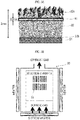
- an uppermost growing surface 22a of the polycrystalline SiC 22 is ground by, for example, 0.2 mm to flat it, and then, a carbon base material-side surface 22b of the polycrystalline SiC 22 is ground by, for example, 1.45 mm. In this way, a base material 11 with a thickness of 0.35 mm is obtained (see the base material 11 in FIG. 2B ).
- an SiC growth step is performed in S20.
- the base material 11 is first loaded into a growth furnace 30.
- a polycrystalline SiC 12 with a thickness of, for example, 400 ⁇ m is grown by chemical vapor deposition. Since this is a chemical vapor deposition using a growth furnace, as shown in FIG. 2B , the polycrystalline SiC 12 grows on a front side and a back side of the base material 11.
- source gas of Si may include tetrachlorosilane, trichlorosilane, and dichlorosilane.
- source gas of C may include ethane, propane, and acetylene.
- a single gas, such as tetramethylsilane, may be used as source gas.
- a growth temperature in this chemical vapor deposition is, for example, 1400°C.
- the base material 11 is formed of polycrystalline SiC.
- the polycrystalline SiC 12 growing from the surface of the base material 11 inherits the crystal structure of the base material 11.
- crystal grains are already large and enlargement of grain size has almost reached its limit; thus, grain size change at the time of growing on the base material 11 is small.
- This makes it possible to achieve a polycrystalline SiC grown homogeneously in a depth direction of the substrate, and a stress generated inside the substrate can thereby be reduced. As a result, it is possible to reduce warpage of the support substrate 2 formed of the polycrystalline SiC 12.
- a separating step is performed in S30.
- a position at a depth of, for example, 400 ⁇ m from a surface of the polycrystalline SiC 12 is irradiated with laser light LS (wavelength: 532 nm), to thereby sublimate SiC.
- a two-dimensional scanning is performed with the laser light LS along a plane parallel to a contact interface where the polycrystalline SiC 12 contacts the base material 11. This results in formation of a cutting plane at a position of 400 ⁇ m from the surface, and the polycrystalline SiC 12 is separated from the base material 11.
- a surface polishing step is performed in S40.
- an amorphous layer formed on the surface of the polycrystalline SiC 12 is removed and the surface of the polycrystalline SiC 12 is smoothed first by high-precision grinding and then by CMP polishing.
- the polycrystalline SiC 12 obtained after the surface polishing step is used as the support substrate 2.
- an amorphous layer formed on the surface of the base material 11 is removed by hydrogen gas supplied in the process of raising the temperature in the growth furnace 30. That is, a second base material 11 can be reused for manufacturing the support substrate 2.
- a bonding step is performed in S50.
- hydrogen ions having implantation energy set in advance according to a thickness of the semiconductor layer 3 are implanted from a front side of a single crystal SiC substrate prepared in advance, toward a surface of the single crystal SiC substrate.
- an ion-implanted layer is formed at a specified depth from the surface of the single crystal SiC substrate according to the implantation energy.
- the surface of the single crystal SiC substrate is bonded to the surface of the polycrystalline SiC 12 manufactured in S40 by a surface activation technique. Then, the polycrystalline SiC 12 and the single crystal SiC substrate bonded together are heated.
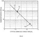
- FIG. 5 is a graph showing a correlation between a radius of curvature of warpage of the support substrate and a crystal grain size change rate of the support substrate.
- a radius of curvature of warpage of a substrate is a radius of a circle, which best approximates the degree of curvature caused by warping of the substrate.
- a crystal grain size change rate of a substrate is a value obtained by dividing a difference between the average value of crystal grain sizes on the front side of the substrate and the average value of crystal grain sizes on the back side of the substrate by a thickness of the substrate.
- the crystal grain size was calculated as an area equivalent circle diameter, which is a diameter converted based on a circle having the same area as each crystal grain.
- Distribution of crystal grains on the front side and the back side of the support substrate is obtained by measuring a crystalline orientation and so on on the front side and the back side of the support substrate using a well-known electron backscatter diffraction (EBSD) analysis.
- EBSD electron backscatter diffraction
- the radius of curvature of the warpage when the crystal grain size change rate is 0.57% is 69 ⁇ m.
- the radius of curvature of the warpage when the crystal grain size change rate is 1.14% is 3 ⁇ m.
- the crystal grain size change rate of 0.43% or less enables the radius of curvature of the warpage to be 142 m or more.
- FIG. 6A is a picture showing distribution of crystal grains on a front side of a support substrate having a crystal grain size change rate of 0.57%.
- FIG. 6B is a histogram showing distribution of crystal grain sizes on the front side of the support substrate having the crystal grain size change rate of 0.57%.
- the average value of the crystal grain sizes on the front side of the support substrate is 12 ⁇ m.
- FIG. 6C is a picture showing distribution of crystal grains on a back side of the support substrate having the crystal grain size change rate of 0.57%.
- FIG. 6D is a histogram showing distribution of crystal grain sizes on the back side of the support substrate having the crystal grain size change rate of 0.57%.
- the average value of the crystal grain sizes on the back side of the support substrate is 10 ⁇ m.
- FIG. 7A is a picture showing distribution of crystal grains on a front side of a support substrate having a crystal grain size change rate of 1.14%.
- FIG. 7B is a histogram showing distribution of crystal grain sizes on the front side of the support substrate having the crystal grain size change rate of 1.14%.
- the average value of the crystal grain sizes on the front side of the support substrate is 11 ⁇ m.
- FIG. 7C is a picture showing distribution of crystal grains on a back side of the support substrate having the crystal grain size change rate of 1.14%.
- FIG. 7D is a histogram showing distribution of crystal grain sizes on the back side of the support substrate having the crystal grain size change rate of 1.14%. The average value of the crystal grain sizes on the back side of the support substrate is 7 ⁇ m.
- the polycrystalline SiC 12 growing from the surface of the base material 11 inherits the crystal structure of the base material 11.
- the thus-configured support substrate 2 which is a polycrystalline SiC substrate formed of polycrystalline SiC, has the crystal grain size change rate of 0.43% or less, and the radius of curvature of the warpage of the polycrystalline SiC substrate is 142 m or more.
- the thus-configured support substrate 2 makes it possible to reduce the influence of the residual stress within the polycrystalline SiC substrate owing to the decreased substrate grain size change rate, and the warpage of the polycrystalline SiC substrate can thereby be reduced.
- the method for manufacturing the support substrate 2 comprises the base material preparation step, the SiC growth step, and the separating step, and the crystal grain size change rate of the base material 11 is 0.43% or less.
- the polycrystalline SiC 22 is grown on the carbon base material 21 formed of carbon under a first growth condition set in advance (chemical vapor deposition at the growth temperature of 1400°C, in the present embodiment), and then the polycrystalline SiC 22 grown on the carbon base material 21 is cut out, to thereby prepare the base material 11 formed of polycrystalline SiC (S10).
- the polycrystalline SiC 12 is grown on the base material 11 under a second growth condition set in advance (chemical vapor deposition at the growth temperature of 1400°C, in the present embodiment) (S20).
- the separating step the polycrystalline SiC 12 grown on the base material 11 is separated from the second base material by irradiation with the laser light LS, and the separated polycrystalline SiC 12 is used as the support substrate 2 (S30).
- the polycrystalline SiC is grown on the base material 11 formed of the polycrystalline SiC. That is, the material of the base material 11 is the same as SiC to be grown thereon.
- the SiC growth step it is possible to achieve the growth of SiC that has inherited the crystal grain size and the crystalline orientation of the surface of the base material 11.
- use of the base material 11 having the crystal grain size change rate of 0.43% or less makes it possible to grow the polycrystalline SiC having the crystal grain size change rate of 0.43% or less on the base material 11. This enables reduction of warpage of the polycrystalline SiC substrate.
- the method for manufacturing the support substrate 2 makes it unnecessary to cut out a portion whose crystal grain size is uniform in the SiC in order to manufacture the polycrystalline SiC substrate.
- the method for manufacturing the support substrate 2 it is unnecessary to grow SiC not to be used as the polycrystalline SiC substrate on the base material.
- the method for manufacturing the support substrate 2 need not include the step of growing, on the base material, redundant SiC not to be used as the polycrystalline SiC substrate or the step of cutting out the portion whose crystal grain size is uniform in the SiC. This can significantly simplify the manufacturing steps.
- the support substrate 2 corresponds to a polycrystalline SiC substrate of the present disclosure
- the front side of the support substrate 2 corresponds to a first side of the present disclosure
- the back side of the support substrate 2 corresponds to a second side of the present disclosure
- the crystal grain size change rate of the support substrate 2 corresponds to a substrate grain size change rate of the present disclosure
- the step of S10 corresponds to a base material preparation step of the present disclosure
- the step of S20 corresponds to an SiC growth step of the present disclosure
- the step of S30 corresponds to a separation step of the present disclosure.
- the carbon base material 21 corresponds to a first base material of the present disclosure
- the base material 11 corresponds to a second base material of the present disclosure
- the crystal grain size change rate of the base material 11 corresponds to a base material grain size change rate of the present disclosure.
- the polycrystalline SiC 12 is separated from the base material 11 by irradiation with the laser light.
- the polycrystalline SiC 12 may be separated by a wire electric discharge machining technique or a wire saw cutting technique, which are well known.
- the base material 11 may be colored by introducing impurities into the polycrystalline SiC 22. This makes it possible to irradiate an interface between the base material 11 and the polycrystalline SiC 12 with the laser light with high accuracy. Consequently, the surface of the base material 11 after the polycrystalline SiC 12 is separated from the base material 11 in the separating step is flatter. Thus, the base material 11 can be reused without performing a process of grinding the surface of the base material 11, whereby the process for reuse of the base material 11 can be simplified.
- the resistivity of the polycrystalline SiC 12 has to be lowered in order to use it for a bonded SiC substrate for use in a high-voltage/high-power electronic element.
- impurities such as, for example, nitrogen and phosphorus are introduced into the polycrystalline SiC 12, and the polycrystalline SiC 12 is colored by such introduction of the impurities.
- the laser light does not reach the interface between the base material 11 and the polycrystalline SiC 12; thus, separating at the interface between the base material 11 and the polycrystalline SiC 12 is difficult.
- a form may be employed in which the polycrystalline SiC 12 on a back side is first separated from the base material 11 using another technique and then the back side of the base material 11 is irradiated with the laser light LS to thereby separate the polycrystalline SiC 12 from the base material 11.
- a form may be employed in which the polycrystalline SiC 12 is grown only on the front side of the base material 11 by forming a protective material on the back side of the base material 11 in advance or by arranging the base material 11 in the growth furnace 30 with the back side of the base material 11 unexposed, and then the back side of the base material 11 is irradiated with the laser light LS to thereby separate the polycrystalline SiC 12 from the base material 11.
- the form in which the polycrystalline SiC 12 is grown by chemical vapor deposition in the SiC growth step is the form in which the polycrystalline SiC 12 is grown by chemical vapor deposition in the SiC growth step.
- a form may be employed in which impurities that generate carriers are introduced to achieve uniform diffusion of, for example, nitrogen or phosphorus within the polycrystalline SiC 12.
- the method for manufacturing the bonded substrate 1 formed of the support substrate 2 and the semiconductor layer 3 bonded together is the method for manufacturing the bonded substrate 1 formed of the support substrate 2 and the semiconductor layer 3 bonded together.
- the degree of surface roughness represented by an arithmetic average roughness be 1 nm or less on at least one of the front side or the back side of the support substrate 2.
- all recesses formed on the front side and the back side be each such that the distance between the front side or the back side and a point in the recess farthest from the front side or the back side, respectively, is 3 nm or less.
- the thus-configured support substrate 2 owing to the surface thereof being less uneven, makes it possible, in manufacturing the bonded substrate 1 in which the semiconductor layer 3 formed of the single crystal SiC is bonded onto the support substrate 2, to increase the bonding strength in the bonded surface between the semiconductor layer 3 and the support substrate 2. Consequently, yields of the bonded substrate 1 can be improved.
- the polycrystalline SiC is grown by chemical vapor deposition in the base material preparation step of S10 and in the SiC growth step of S20.
- the polycrystalline SiC may be grown using a sublimation method in which an SiC raw material is sublimated and then crystallized.
Landscapes
- Chemical & Material Sciences (AREA)
- Engineering & Computer Science (AREA)
- Organic Chemistry (AREA)
- Materials Engineering (AREA)
- Metallurgy (AREA)
- Crystallography & Structural Chemistry (AREA)
- Chemical Kinetics & Catalysis (AREA)
- Inorganic Chemistry (AREA)
- General Chemical & Material Sciences (AREA)
- Ceramic Engineering (AREA)
- Mechanical Engineering (AREA)
- Manufacturing & Machinery (AREA)
- Structural Engineering (AREA)
- Crystals, And After-Treatments Of Crystals (AREA)
Applications Claiming Priority (2)
| Application Number | Priority Date | Filing Date | Title |
|---|---|---|---|
| JP2016075920 | 2016-04-05 | ||
| PCT/JP2017/014248 WO2017175799A1 (fr) | 2016-04-05 | 2017-04-05 | SUBSTRAT DE SiC POLYCRISTALLIN ET PROCÉDÉ POUR SA FABRICATION |
Publications (2)
| Publication Number | Publication Date |
|---|---|
| EP3441506A1 true EP3441506A1 (fr) | 2019-02-13 |
| EP3441506A4 EP3441506A4 (fr) | 2019-12-11 |
Family
ID=60000403
Family Applications (1)
| Application Number | Title | Priority Date | Filing Date |
|---|---|---|---|
| EP17779177.9A Pending EP3441506A4 (fr) | 2016-04-05 | 2017-04-05 | SUBSTRAT DE SiC POLYCRISTALLIN ET PROCÉDÉ POUR SA FABRICATION |
Country Status (6)
| Country | Link |
|---|---|
| US (1) | US10934634B2 (fr) |
| EP (1) | EP3441506A4 (fr) |
| JP (1) | JP6619874B2 (fr) |
| KR (1) | KR102109292B1 (fr) |
| CN (1) | CN108884593B (fr) |
| WO (1) | WO2017175799A1 (fr) |
Cited By (5)
| Publication number | Priority date | Publication date | Assignee | Title |
|---|---|---|---|---|
| FR3127842A1 (fr) | 2021-10-05 | 2023-04-07 | Soitec | Structure composite comprenant une couche utile en sic monocristallin sur un substrat support en sic poly-cristallin et procede de fabrication de ladite structure |
| FR3139413A1 (fr) * | 2022-09-05 | 2024-03-08 | Soitec | Procédé de traitement d’une plaquette de carbure de silicium polycristallin |
| EP4439630A1 (fr) * | 2023-03-31 | 2024-10-02 | STMicroelectronics International N.V. | Substrat de carbure de silicium polycristallin et son procédé de fabrication |
| EP4439629A1 (fr) * | 2023-03-31 | 2024-10-02 | STMicroelectronics International N.V. | Substrat ou tranche polycristallin a faible resistivite |
| EP4528787A1 (fr) * | 2023-09-25 | 2025-03-26 | STMicroelectronics International N.V. | Substrat de carbure de silicium (sic) polycristallin à résistivité élevée et son procédé de fabrication |
Families Citing this family (19)
| Publication number | Priority date | Publication date | Assignee | Title |
|---|---|---|---|---|
| CN107190322B (zh) * | 2017-04-01 | 2019-06-11 | 中国科学院上海硅酸盐研究所 | 一种大尺寸电阻率可调的碳化硅多晶陶瓷的生长方法 |
| DE102019111377B4 (de) * | 2018-05-28 | 2025-10-09 | Infineon Technologies Ag | Verfahren zum Verarbeiten eines Siliziumkarbid-Wafers |
| JP7235456B2 (ja) * | 2018-08-14 | 2023-03-08 | 株式会社ディスコ | 半導体基板の加工方法 |
| JP7322371B2 (ja) * | 2018-09-27 | 2023-08-08 | 住友金属鉱山株式会社 | 炭化珪素多結晶基板の製造方法 |
| WO2021020574A1 (fr) * | 2019-08-01 | 2021-02-04 | ローム株式会社 | Substrat semi-conducteur , dispositif à semi-conducteur et leurs procédés de production |
| EP4206366A4 (fr) * | 2020-08-28 | 2024-11-06 | Kyocera Corporation | Procédé de fabrication de polycristal de sic |
| JP7298940B2 (ja) | 2020-09-22 | 2023-06-27 | セニック・インコーポレイテッド | 炭化珪素ウエハ及びその製造方法 |
| FR3127330B1 (fr) | 2021-09-22 | 2023-09-22 | Soitec Silicon On Insulator | Procede de fabrication d’un substrat support en carbure de silicium poly-cristallin |
| JP2023061509A (ja) * | 2021-10-20 | 2023-05-02 | 株式会社サイコックス | 多結晶炭化珪素基板の製造方法 |
| FR3130296B1 (fr) * | 2021-12-14 | 2023-11-03 | Soitec Silicon On Insulator | Procede de fabrication d’une structure semi-conductrice comprenant un substrat de carbure de silicium polycristallin et une couche active de carbure de silicium monocristallin |
| FR3134228B1 (fr) | 2022-03-30 | 2025-05-02 | Mersen France Gennevilliers | Procede de fabrication de carbure de silicium polycristallin utilisable pour la fabrication de substrats de circuits integres, et carbure de silicium ainsi obtenu |
| FR3134234B1 (fr) | 2022-03-30 | 2024-02-23 | Soitec Silicon On Insulator | Structure composite comprenant une couche mince monocristalline sur un substrat support en carbure de silicium poly-cristallin et procede de fabrication associe |
| FR3142829B1 (fr) * | 2022-12-05 | 2026-01-02 | Soitec Silicon On Insulator | Procédé de fabrication d’un substrat pour un dispositif électronique de puissance ou radiofréquence |
| FR3146236B1 (fr) | 2023-02-24 | 2025-01-17 | Soitec Silicon On Insulator | Structure composite comprenant une couche mince monocristalline sur un substrat support en carbure de silicium poly-cristallin et procede de fabrication associe |
| FR3146237A1 (fr) | 2023-02-24 | 2024-08-30 | Mersen France Gennevilliers | Plaque en SiC polycristallin dopé à planéité et conductivité électrique améliorées, et procédé de fabrication d’une telle plaque |
| US20240332366A1 (en) * | 2023-03-31 | 2024-10-03 | Stmicroelectronics International N.V. | Polycrystalline silicon carbide substrate with density gradient and method of manufacturing the same |
| FR3153463B1 (fr) * | 2023-09-26 | 2025-10-17 | Soitec Silicon On Insulator | ProcÉdÉ de transfert d’un couche de SiC monocristallin sur un support en SiC polycristallin utilisant un substrat temporaire de SiC monocristallin |
| EP4632118A1 (fr) * | 2024-04-09 | 2025-10-15 | SiCrystal GmbH | Substrat stratifié, procédé de fabrication d'un substrat stratifié et procédé de croissance d'une couche épitaxiale avec le substrat stratifié |
| EP4632116A1 (fr) * | 2024-04-09 | 2025-10-15 | SiCrystal GmbH | Germe stratifié, procédé de fabrication d'un germe stratifié et procédé de croissance d'un monocristal volumique à l'aide du germe stratifié |
Family Cites Families (19)
| Publication number | Priority date | Publication date | Assignee | Title |
|---|---|---|---|---|
| JPH08188468A (ja) | 1994-12-29 | 1996-07-23 | Toyo Tanso Kk | 化学蒸着法による炭化ケイ素成形体及びその製造方法 |
| JPH08188408A (ja) * | 1994-12-29 | 1996-07-23 | Toyo Tanso Kk | 化学蒸着法による炭化ケイ素成形体及びその製造方法 |
| JP3524679B2 (ja) * | 1996-06-21 | 2004-05-10 | 東芝セラミックス株式会社 | 高純度CVD−SiC質の半導体熱処理用部材及びその製造方法 |
| JPH1179846A (ja) * | 1997-09-01 | 1999-03-23 | Tokai Carbon Co Ltd | 炭化珪素成形体 |
| JP3648112B2 (ja) * | 1999-11-26 | 2005-05-18 | 東芝セラミックス株式会社 | CVD−SiC自立膜構造体、及びその製造方法 |
| US20100297350A1 (en) * | 2003-12-05 | 2010-11-25 | David Thomas Forrest | Free-standing silicon carbide articles formed by chemical vapor deposition and methods for their manufacture |
| JP4974986B2 (ja) | 2007-09-28 | 2012-07-11 | 富士フイルム株式会社 | 太陽電池用基板および太陽電池 |
| WO2012086239A1 (fr) | 2010-12-24 | 2012-06-28 | 東洋炭素株式会社 | Substance de base pour croissance épitaxiale du carbure de silicium monocristallin, et procédé de croissance épitaxiale du carbure de silicium monocristallin |
| EP2657374A4 (fr) * | 2010-12-24 | 2014-05-07 | Toyo Tanso Co | Unité pour croissance épitaxiale en phase liquide du carbure de silicium monocristallin, et procédé de croissance épitaxiale en phase liquide du carbure de silicium monocristallin |
| JP5840366B2 (ja) * | 2011-01-06 | 2016-01-06 | 株式会社デンソー | 炭化珪素半導体基板の製造方法および炭化珪素半導体装置の製造方法 |
| JP2013067522A (ja) * | 2011-09-21 | 2013-04-18 | Sumitomo Electric Ind Ltd | 炭化珪素結晶の製造方法 |
| JP6061251B2 (ja) | 2013-07-05 | 2017-01-18 | 株式会社豊田自動織機 | 半導体基板の製造方法 |
| JP6195426B2 (ja) * | 2014-04-18 | 2017-09-13 | 国立研究開発法人産業技術総合研究所 | 炭化珪素エピタキシャルウエハおよびその製造方法 |
| WO2016113924A1 (fr) * | 2015-01-13 | 2016-07-21 | 住友電気工業株式会社 | Stratifié semi-conducteur |
| JP6544166B2 (ja) * | 2015-09-14 | 2019-07-17 | 信越化学工業株式会社 | SiC複合基板の製造方法 |
| JP6582779B2 (ja) * | 2015-09-15 | 2019-10-02 | 信越化学工業株式会社 | SiC複合基板の製造方法 |
| JP6515757B2 (ja) * | 2015-09-15 | 2019-05-22 | 信越化学工業株式会社 | SiC複合基板の製造方法 |
| JP6481582B2 (ja) * | 2015-10-13 | 2019-03-13 | 住友電気工業株式会社 | 炭化珪素エピタキシャル基板および炭化珪素半導体装置の製造方法 |
| FR3048306B1 (fr) * | 2016-02-26 | 2018-03-16 | Soitec | Support pour une structure semi-conductrice |
-
2017
- 2017-04-05 JP JP2018510638A patent/JP6619874B2/ja active Active
- 2017-04-05 EP EP17779177.9A patent/EP3441506A4/fr active Pending
- 2017-04-05 CN CN201780022271.9A patent/CN108884593B/zh active Active
- 2017-04-05 US US16/091,459 patent/US10934634B2/en active Active
- 2017-04-05 KR KR1020187031205A patent/KR102109292B1/ko active Active
- 2017-04-05 WO PCT/JP2017/014248 patent/WO2017175799A1/fr not_active Ceased
Cited By (7)
| Publication number | Priority date | Publication date | Assignee | Title |
|---|---|---|---|---|
| FR3127842A1 (fr) | 2021-10-05 | 2023-04-07 | Soitec | Structure composite comprenant une couche utile en sic monocristallin sur un substrat support en sic poly-cristallin et procede de fabrication de ladite structure |
| WO2023057699A1 (fr) | 2021-10-05 | 2023-04-13 | Soitec | Structure composite comprenant une couche utile en sic monocristallin sur un substrat support en sic poly-cristallin et procede de fabrication de ladite structure |
| FR3139413A1 (fr) * | 2022-09-05 | 2024-03-08 | Soitec | Procédé de traitement d’une plaquette de carbure de silicium polycristallin |
| WO2024052615A1 (fr) * | 2022-09-05 | 2024-03-14 | Soitec | Procede de traitement d'une plaquette de carbure de silicium polycristallin |
| EP4439630A1 (fr) * | 2023-03-31 | 2024-10-02 | STMicroelectronics International N.V. | Substrat de carbure de silicium polycristallin et son procédé de fabrication |
| EP4439629A1 (fr) * | 2023-03-31 | 2024-10-02 | STMicroelectronics International N.V. | Substrat ou tranche polycristallin a faible resistivite |
| EP4528787A1 (fr) * | 2023-09-25 | 2025-03-26 | STMicroelectronics International N.V. | Substrat de carbure de silicium (sic) polycristallin à résistivité élevée et son procédé de fabrication |
Also Published As
| Publication number | Publication date |
|---|---|
| JP6619874B2 (ja) | 2019-12-11 |
| KR102109292B1 (ko) | 2020-05-11 |
| CN108884593A (zh) | 2018-11-23 |
| US20190153616A1 (en) | 2019-05-23 |
| CN108884593B (zh) | 2021-03-12 |
| KR20180126566A (ko) | 2018-11-27 |
| JPWO2017175799A1 (ja) | 2018-11-08 |
| EP3441506A4 (fr) | 2019-12-11 |
| WO2017175799A1 (fr) | 2017-10-12 |
| US10934634B2 (en) | 2021-03-02 |
Similar Documents
| Publication | Publication Date | Title |
|---|---|---|
| US10934634B2 (en) | Polycrystalline SiC substrate and method for manufacturing same | |
| JP2026048816A (ja) | 大口径炭化ケイ素ウェハ | |
| JP5304713B2 (ja) | 炭化珪素単結晶基板、炭化珪素エピタキシャルウェハ、及び薄膜エピタキシャルウェハ | |
| TWI330206B (en) | Seventy five millimeter silicon carbide wafer with low warp, bow, and ttv | |
| JP4964672B2 (ja) | 低抵抗率炭化珪素単結晶基板 | |
| JP5569112B2 (ja) | 炭化珪素単結晶ウェハの製造方法及びこの方法で得られた炭化珪素単結晶ウェハ | |
| CN105579626A (zh) | 碳化硅半导体衬底及其制造方法 | |
| US11795576B2 (en) | Production method of silicon carbide wafer, production method of semiconductor substrate, and production method of silicon carbide semiconductor device | |
| JPWO2015182474A1 (ja) | 炭化珪素インゴットの製造方法、炭化珪素種基板、炭化珪素基板、半導体装置および半導体装置の製造方法 | |
| US8642153B2 (en) | Single crystal silicon carbide substrate and method of manufacturing the same | |
| US11948794B2 (en) | Method of manufacturing silicon carbide epitaxial wafer | |
| CN103828027A (zh) | 制造碳化硅衬底的方法和碳化硅衬底 | |
| US8729676B2 (en) | Silicon epitaxial wafer and method for manufacturing the same | |
| JP6748613B2 (ja) | 炭化珪素単結晶基板 | |
| JP7143769B2 (ja) | 炭化珪素半導体基板の製造方法及び炭化珪素半導体装置の製造方法 | |
| JP7816659B1 (ja) | SiC接合基板及び半導体デバイス | |
| CN115398047A (zh) | 氮化铝衬底的制造方法、氮化铝衬底以及抑制位错向氮化铝生长层引入的方法 | |
| JP2021070617A (ja) | 炭化珪素エピ基板の製造方法及び半導体装置の製造方法 | |
| JP7782766B1 (ja) | SiC多結晶基板、SiC貼り合わせ基板、及び、SiC多結晶基板の製造方法 | |
| TW202435283A (zh) | 碳化矽半導體裝置用基板、碳化矽接合基板、碳化矽多結晶基板及碳化矽多結晶基板之製造方法 | |
| CN119545874A (zh) | SiC基板及SiC外延晶片 | |
| TW202513910A (zh) | SiC半導體裝置用基板,SiC接合基板,SiC多結晶基板及SiC多結晶基板的製造方法 | |
| CN120113032A (zh) | 异质外延基板的制造方法 |
Legal Events
| Date | Code | Title | Description |
|---|---|---|---|
| STAA | Information on the status of an ep patent application or granted ep patent |
Free format text: STATUS: THE INTERNATIONAL PUBLICATION HAS BEEN MADE |
|
| PUAI | Public reference made under article 153(3) epc to a published international application that has entered the european phase |
Free format text: ORIGINAL CODE: 0009012 |
|
| STAA | Information on the status of an ep patent application or granted ep patent |
Free format text: STATUS: REQUEST FOR EXAMINATION WAS MADE |
|
| 17P | Request for examination filed |
Effective date: 20181019 |
|
| AK | Designated contracting states |
Kind code of ref document: A1 Designated state(s): AL AT BE BG CH CY CZ DE DK EE ES FI FR GB GR HR HU IE IS IT LI LT LU LV MC MK MT NL NO PL PT RO RS SE SI SK SM TR |
|
| AX | Request for extension of the european patent |
Extension state: BA ME |
|
| DAV | Request for validation of the european patent (deleted) | ||
| DAX | Request for extension of the european patent (deleted) | ||
| A4 | Supplementary search report drawn up and despatched |
Effective date: 20191111 |
|
| RIC1 | Information provided on ipc code assigned before grant |
Ipc: C30B 29/36 20060101AFI20191105BHEP Ipc: C30B 28/12 20060101ALI20191105BHEP Ipc: H01L 21/02 20060101ALI20191105BHEP |
|
| TPAC | Observations filed by third parties |
Free format text: ORIGINAL CODE: EPIDOSNTIPA |
|
| STAA | Information on the status of an ep patent application or granted ep patent |
Free format text: STATUS: EXAMINATION IS IN PROGRESS |
|
| 17Q | First examination report despatched |
Effective date: 20220825 |
|
| RIN1 | Information on inventor provided before grant (corrected) |
Inventor name: KOBAYASHI, MOTOKI Inventor name: YAGI, KUNIAKI |
|
| REG | Reference to a national code |
Ref country code: DE Ref legal event code: R003 |
|
| STAA | Information on the status of an ep patent application or granted ep patent |
Free format text: STATUS: THE APPLICATION HAS BEEN REFUSED |