EP3444953B1 - Appareil et procédé de correspondance de fréquence radio pour terminal de communication portable - Google Patents
Appareil et procédé de correspondance de fréquence radio pour terminal de communication portable Download PDFInfo
- Publication number
- EP3444953B1 EP3444953B1 EP18199367.6A EP18199367A EP3444953B1 EP 3444953 B1 EP3444953 B1 EP 3444953B1 EP 18199367 A EP18199367 A EP 18199367A EP 3444953 B1 EP3444953 B1 EP 3444953B1
- Authority
- EP
- European Patent Office
- Prior art keywords
- matching
- communication terminal
- portable communication
- control apparatus
- matching control
- Prior art date
- Legal status (The legal status is an assumption and is not a legal conclusion. Google has not performed a legal analysis and makes no representation as to the accuracy of the status listed.)
- Active
Links
Images

Classifications
-
- H—ELECTRICITY
- H04—ELECTRIC COMMUNICATION TECHNIQUE
- H04B—TRANSMISSION
- H04B1/00—Details of transmission systems, not covered by a single one of groups H04B3/00 - H04B13/00; Details of transmission systems not characterised by the medium used for transmission
- H04B1/06—Receivers
- H04B1/16—Circuits
- H04B1/18—Input circuits, e.g. for coupling to an antenna or a transmission line
-
- H—ELECTRICITY
- H04—ELECTRIC COMMUNICATION TECHNIQUE
- H04B—TRANSMISSION
- H04B1/00—Details of transmission systems, not covered by a single one of groups H04B3/00 - H04B13/00; Details of transmission systems not characterised by the medium used for transmission
- H04B1/02—Transmitters
- H04B1/04—Circuits
- H04B1/0458—Arrangements for matching and coupling between power amplifier and antenna or between amplifying stages
-
- H—ELECTRICITY
- H04—ELECTRIC COMMUNICATION TECHNIQUE
- H04B—TRANSMISSION
- H04B1/00—Details of transmission systems, not covered by a single one of groups H04B3/00 - H04B13/00; Details of transmission systems not characterised by the medium used for transmission
- H04B1/38—Transceivers, i.e. devices in which transmitter and receiver form a structural unit and in which at least one part is used for functions of transmitting and receiving
- H04B1/40—Circuits
Definitions
- the present invention relates to a portable communication terminal and, in particular, to a Radio Frequency (RF) matching control apparatus and method for a portable communication terminal.
- RF Radio Frequency
- a portable communication terminal is implemented so as to optimize a radiation characteristic.
- the portable communication terminal inevitably suffers from degradations in reception sensitivity and transmission power due to the radiation characteristic variation in accordance with the change of channel environment.
- each RF matching circuit should be implemented with resistors, inductors, and capacitors, having preset resistances, inductances, and capacitances, respectively. That is, the values of the elements constituting each RF matching circuit are fixed in the manufacturing stage and each RF matching circuit operates independently.
- the conventional multiple RF matching circuits-based portable communication terminal is disadvantageous in that the increase in the number of the RF matching circuits requires additional space, resulting in difficulty of compact design.
- the limited number of the RF matching circuits causes limitation of RF tuning performance of the portable communication terminal.
- WO 2005/112280 discloses position sensors which detect the position of a user's hand position on a mobile communication device.
- a controller dynamically adjusts the source impedance of a transmitter and/or receiver in the mobile communication device based on the user's hand position to compensate for variations in the load impedance caused by the user's hand position.
- US 2003/096583 discloses that, in a mobile radio apparatus, a matching circuit is selected to meet the detected condition detected by a switching control unit. Matching of the antenna to the RF circuit can be optimized and the antenna gain deterioration can be prevented.
- WO 96/39727 discloses an automatic antenna tuner which conjugately matches the impedance of an electrically small antenna to the impedance of a transmit amplifier output stage by using a pi-type impedance matching network with adjustable capacitive circuit components which are preferably implemented using a low-cost escapement mechanism.
- the present invention has been made in an effort to solve the above problems, and it is an object of the present invention to provide an RF matching control apparatus and method for a portable communication terminal that are capable of optimizing a reception sensitivity and a transmission power.
- a Radio Frequency (RF) matching control apparatus for a portable communication terminal according to claim 1 and a Radio Frequency (RF) matching control method according to claim 15.
- the RF matching circuitry includes at least one unit cell.
- the unit cell includes at least two matching circuits including resistors, inductors, and capacitors of different values.
- the RF matching circuitry includes 2 stepwise unit cells and each unit cell includes 8 matching circuits.
- the quantity of the unit cells and of the matching circuits per unit cell can be changed.
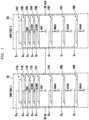
- an RF matching circuitry includes first and second unit cells 10 and 20 connected in series between a radio frequency input terminal (RF in) connected to an antenna (not shown) and a radio frequency output terminal (RF out), for matching a radio frequency signal received through the radio frequency input terminal (RF in) and transferring the matched radio frequency signal to the radio frequency output terminal (RF out).
- RF in radio frequency input terminal
- RF out radio frequency output terminal
- First and second unit cells 10 and 20 each include devices such as resistors, inductors, and capacitors connected in series or parallel with each other.
- First unit cell 10 includes matching circuits 108, 109, 110, 111, 112, 113, 114, and 115 interposed in parallel between the radio frequency input terminal (RF in) and the second unit cell 20, and the second unit cell 20 includes matching circuits 100, 101, 102, 103, 104, 105, 106, and 107 interposed in parallel between the first unit cell 10 and the radio frequency output terminal (RF out).
- Matching circuit 108 includes a grounded 64nH inductor
- Matching circuit 109 includes a grounded 47nH inductor
- tenth matching circuit 110 includes a grounded 30nh inductor.
- Matching circuit 111 includes a grounded 4pF capacitor
- matching circuit 112 includes a 4.7nH inductor connected in series
- matching circuit 113 includes a 2.7nH inductor connected in series
- matching circuit 114 includes a 4pF capacitor connected in series
- matching circuit 115 includes a resistors connected in series.
- Matching circuit 100 includes a grounded 64nH inductor, matching circuit 101 includes a grounded 47nH inductor, and matching circuit 102 includes a grounded 30nH inductor.
- Matching circuit 103 includes a grounded 4pF capacitor
- matching circuit 104 includes a 4.7nH inductor connected in series
- matching circuit 105 includes a 2.7nH inductor connected in series
- matching circuit 106 includes a 4pF capacitor connected in series
- matching circuit 107 includes a resistor connected in series.
- each matching circuit includes at least one matching device 202 connected between a pair of switches 201 and 203 that are connected to an input terminal and an output terminal of matching device 202, respectively.
- Matching device 202 can be a resistor, an inductor, or a capacitor. Switches 201 and 203 of each matching circuit are connected to a decoding unit (see FIG. 3 ).
- decoding unit 5 includes a decoder 30 and a buffer 40.
- Decoder 30 generates the control signals for controlling switches 201 and 203 connected to the input and output terminals, respectively, of matching device 202.
- the decoder is preferably implemented as a 4*16 decoder in consideration of the RF matching circuitry of FIG. 1 .
- RF matching circuitry includes two unit cells 10 and 20, each unit cell including 8 matching circuits, such that decoder 30 generates control signals for selecting one matching circuit from each of first and second unit cells 10 and 20.
- decoding unit 5 includes a decoder 30 that generates condition values for selecting matching circuits according to an environment of the portable communication terminal, and a buffer 40 for temporarily storing the condition values generated by decoder 30.
- the condition values stored in buffer 40 are updated by a signal input through a strobe terminal.
- matching circuits 100 to 115 are connected to buffer 40 of decoding unit 5 through respective signal lines, and each of switches 201 and 203 installed at the input and output terminals of each matching device 202 is either on or off simultaneously according to the state of buffer 40.
- the RF matching circuitry of the present invention operates according to the condition values determined by the environment of the portable communication terminal, it is possible to optimize the RF matching adaptively to the environment.
- the portable communication terminal initializes buffer 40.
- the initial value is '0000' and the strobe is in a deactivated state by a pull-up resistance.
- the number of cases of 4 condition values is 16 and can be represented as in Table 1. If a 4 bit-value is input to decoding unit 5, 16 unique status values are output such that the switches are turned on and off according to the corresponding status values.
- condition values are determined according to variations in the environment of the portable communication terminal. For example, when a folder of the portable communication terminal is opened or closed (or a slide body is moved up or down) the portable communication terminal retrieves values corresponding to the status of the folder or the slide body from a condition value table.
- the condition values are predetermined as shown in Table 2.
- Buffer 40 of the decoding unit 5 is updated by an of the portable communication terminal transmitting a strobe value from 'high' to 'low'.
- the condition value is automatically selected in a software supported manner and the strobe is activated such that the RF matching is controlled according to the condition value, resulting in optimization of the reception sensitivity and transmission power.
- the RF matching circuitry and method of the present invention can be implemented in the form of a universal integrated chip (IC) and can operate adaptively with respect to the environment of a portable communication terminal, whereby it is possible to improve transmission and reception characteristics and prevent the reception sensitivity from degradation by influence of a human body in a weak electric field.
- IC universal integrated chip
- the RF matching circuitry of the present invention can be tuned to operate such that the reception sensitivity is developed relative to the transmission power in a weak receive electric field and the transmission power increases relative to the reception sensitivity in a weak transmit electric field.
- the RF matching circuitry of the present invention can effectively manage the transmission power adaptively to the utilization environment of the portable communication terminal, resulting in an increase of battery life.
- the RF matching circuitry of the present invention can tune the RF matching characteristics in a software-supported manner, whereby it is possible to reduce the time and labor for developing a matching circuit for obtaining a specific radiation characteristic.
Landscapes
- Engineering & Computer Science (AREA)
- Computer Networks & Wireless Communication (AREA)
- Signal Processing (AREA)
- Transceivers (AREA)
- Transmitters (AREA)
- Telephone Function (AREA)
- Mobile Radio Communication Systems (AREA)
Claims (15)
- Appareil de commande d'adaptation radiofréquence (RF) pour un terminal de communication portable, comprenant :une circuiterie d'adaptation permettant d'effectuer une adaptation RF sur une entrée de signal RF par l'intermédiaire d'une antenne et de délivrer entrée un signal RF adapté ; etune unité de décodage (5) permettant de fournir à la circuiterie d'adaptation des signaux de commande d'adaptation selon un environnement du terminal de communication portable,ledit terminal de communication portable comprenant une table de valeurs de condition comportant une pluralité de valeurs de condition, chaque valeur de condition étant déterminée par un état du terminal de communication portable, ledit état du terminal de communication portable étant lié à l'ouverture ou à la fermeture d'un dossier du terminal de communication portable et à une puissance d'un signal Tx ou d'un signal Rx ; etladite unité de décodage (5) étant configurée pour :sélectionner une valeur de condition dans la table de valeurs de condition selon l'environnement et l'état du terminal de communication portable etdéterminer les signaux de commande d'adaptation correspondant à la valeur de condition sélectionnée ;stocker les signaux de commande d'adaptation déterminés ; etfournir les signaux de commande d'adaptation stockés à la circuiterie d'adaptation pour sélectionner au moins un circuit d'adaptation parmi une pluralité de circuits d'adaptation (100-115) constituant la circuiterie d'adaptation selon la valeur de condition sélectionnée.
- Appareil de commande d'adaptation RF selon la revendication 1, ladite circuiterie d'adaptation étant connectée à ladite unité de décodage (5) par l'intermédiaire d'une pluralité de lignes de signaux parallèles (S0-S15).
- Appareil de commande d'adaptation RF selon la revendication 1, ladite circuiterie d'adaptation comprenant une première unité d'adaptation (10) et une seconde unité d'adaptation (20) connectées en série, lesdites première et seconde unités d'adaptation (10, 20) étant connectées à ladite unité de décodage (5) par l'intermédiaire d'une pluralité de lignes de signaux (S0-S15).
- Appareil de commande d'adaptation RF selon la revendication 3, lesdites première et seconde unités d'adaptation (10, 20) comprenant chacune ladite pluralité de circuits d'adaptation (100-115), et au moins un circuit d'adaptation de ladite pluralité de circuits d'adaptation (100-115) étant connecté à ladite unité de décodage (5).
- Appareil de commande d'adaptation RF selon la revendication 4, chaque circuit d'adaptation (100-115) comprenant un dispositif d'adaptation (202), ainsi qu'un commutateur (201) agencé au niveau d'une ligne d'entrée et un commutateur (203) agencé au niveau d'une ligne de sortie dudit dispositif d'adaptation (202).
- Appareil de commande d'adaptation RF selon la revendication 5, lesdits commutateurs (201, 203) étant chacun passants ou non passants selon les signaux de commande d'adaptation fournis.
- Appareil de commande d'adaptation RF selon la revendication 4, chacune desdites première et seconde unités d'adaptation (10, 20) étant capable de connecter au moins deux circuits d'adaptation (100-115) ou plus en parallèle.
- Appareil de commande d'adaptation RF selon la revendication 3, lesdites première et seconde unités d'adaptation (10, 20) comprenant chacune 8 circuits d'adaptation (100-115), et au moins un des circuits d'adaptation (100-115) étant connecté à ladite unité de décodage (5).
- Appareil de commande d'adaptation RF selon la revendication 8, chaque circuit d'adaptation (100-115) comprenant un dispositif d'adaptation (202), ainsi qu'un commutateur (201) agencé au niveau d'une ligne d'entrée et un commutateur (203) agencé au niveau d'une ligne de sortie dudit dispositif d'adaptation (202).
- Appareil de commande d'adaptation RF selon la revendication 9, lesdits commutateurs (201, 203) étant chacun passants ou non passants selon les signaux de commande d'adaptation fournis.
- Appareil de commande d'adaptation RF selon la revendication 3, lesdites première et seconde unités d'adaptation (10, 20) comprenant chacune au moins deux circuits d'adaptation (100-115).
- Appareil de commande d'adaptation RF selon la revendication 11, chaque circuit d'adaptation (100-115) comprenant un dispositif d'adaptation (202) et un ou plusieurs commutateurs (201, 203) permettant de commuter le dispositif d'adaptation (202) dans la circuiterie d'adaptation (100-115).
- Appareil de commande d'adaptation RF selon la revendication 1, ladite unité de décodage (5) étant configurée pour fournir lesdits signaux de commande d'adaptation stockés à ladite circuiterie d'adaptation pour sélectionner et connecter deux circuits d'adaptation (100-115) ou plus constituant ladite circuiterie d'adaptation selon lesdits signaux de commande d'adaptation fournis.
- Appareil de commande d'adaptation RF selon la revendication 1, ladite unité de décodage (5) étant configurée pour entrer un signal stroboscopique permettant de mettre à jour les signaux de commande d'adaptation stockés.
- Procédé de commande d'adaptation radiofréquence (RF) d'un terminal de communication portable comportant une circuiterie d'adaptation RF permettant d'effectuer une adaptation RF sur un signal RF reçu par l'intermédiaire d'une ligne d'entrée connectée à une antenne et de délivrer en sortie un signal RF adapté par l'intermédiaire d'une ligne de sortie, le procédé comprenant :la réception d'un signal RF ;la sélection d'une valeur de condition dans une table de valeurs de condition selon l'environnement et l'état du terminal de communication portable, la table de valeurs de condition comportant une pluralité de valeurs de condition, chaque valeur de condition étant déterminée par un état du terminal de communication portable, l'état du terminal de communication portable étant lié à l'ouverture ou à la fermeture d'un dossier du terminal de communication portable et à une puissance d'un signal Tx ou d'un signal Rx ;la détermination de signaux de commande d'adaptation correspondant à la valeur de condition sélectionnée ;le stockage des signaux de commande d'adaptation déterminés ;la sélection d'au moins un circuit d'adaptation parmi une pluralité de circuits d'adaptation (100-115) constituant la circuiterie d'adaptation RF selon les signaux de commande d'adaptation stockés ; etla réalisation d'une adaptation sur le signal RF reçu, au moyen du circuit d'adaptation (100-115) sélectionné.
Priority Applications (1)
| Application Number | Priority Date | Filing Date | Title |
|---|---|---|---|
| EP25179235.4A EP4604404A3 (fr) | 2006-08-07 | 2007-04-16 | Appareil et procédé de commande d'adaptation de fréquence radio pour terminal de communication portable |
Applications Claiming Priority (2)
| Application Number | Priority Date | Filing Date | Title |
|---|---|---|---|
| KR1020060074205A KR100726260B1 (ko) | 2006-08-07 | 2006-08-07 | 통신 장치의 정합 제어 장치 및 방법 |
| EP07007678.1A EP1887705B1 (fr) | 2006-08-07 | 2007-04-16 | Appareil de contrôle de la correspondance de fréquences radio et procédé pour un terminal de communications portable |
Related Parent Applications (1)
| Application Number | Title | Priority Date | Filing Date |
|---|---|---|---|
| EP07007678.1A Division EP1887705B1 (fr) | 2006-08-07 | 2007-04-16 | Appareil de contrôle de la correspondance de fréquences radio et procédé pour un terminal de communications portable |
Related Child Applications (1)
| Application Number | Title | Priority Date | Filing Date |
|---|---|---|---|
| EP25179235.4A Division EP4604404A3 (fr) | 2006-08-07 | 2007-04-16 | Appareil et procédé de commande d'adaptation de fréquence radio pour terminal de communication portable |
Publications (2)
| Publication Number | Publication Date |
|---|---|
| EP3444953A1 EP3444953A1 (fr) | 2019-02-20 |
| EP3444953B1 true EP3444953B1 (fr) | 2025-05-28 |
Family
ID=38358763
Family Applications (3)
| Application Number | Title | Priority Date | Filing Date |
|---|---|---|---|
| EP25179235.4A Pending EP4604404A3 (fr) | 2006-08-07 | 2007-04-16 | Appareil et procédé de commande d'adaptation de fréquence radio pour terminal de communication portable |
| EP07007678.1A Ceased EP1887705B1 (fr) | 2006-08-07 | 2007-04-16 | Appareil de contrôle de la correspondance de fréquences radio et procédé pour un terminal de communications portable |
| EP18199367.6A Active EP3444953B1 (fr) | 2006-08-07 | 2007-04-16 | Appareil et procédé de correspondance de fréquence radio pour terminal de communication portable |
Family Applications Before (2)
| Application Number | Title | Priority Date | Filing Date |
|---|---|---|---|
| EP25179235.4A Pending EP4604404A3 (fr) | 2006-08-07 | 2007-04-16 | Appareil et procédé de commande d'adaptation de fréquence radio pour terminal de communication portable |
| EP07007678.1A Ceased EP1887705B1 (fr) | 2006-08-07 | 2007-04-16 | Appareil de contrôle de la correspondance de fréquences radio et procédé pour un terminal de communications portable |
Country Status (4)
| Country | Link |
|---|---|
| US (1) | US7761064B2 (fr) |
| EP (3) | EP4604404A3 (fr) |
| KR (1) | KR100726260B1 (fr) |
| CN (2) | CN103138784B (fr) |
Families Citing this family (5)
| Publication number | Priority date | Publication date | Assignee | Title |
|---|---|---|---|---|
| CN103430457B (zh) | 2011-03-24 | 2015-05-13 | 株式会社村田制作所 | 高频模块 |
| US8975981B2 (en) | 2011-09-13 | 2015-03-10 | Qualcomm Incorporated | Impedance matching circuits with multiple configurations |
| US9054756B2 (en) * | 2011-09-19 | 2015-06-09 | Qualcomm Incorporated | Adaptive tuning of an impedance matching circuit in a wireless device |
| US9306603B2 (en) | 2014-01-24 | 2016-04-05 | Qualcomm Incorporated | Tunable radio frequency (RF) front-end architecture using filter having adjustable inductance and capacitance |
| GB2546188B (en) * | 2015-09-02 | 2019-07-03 | Skyworks Solutions Inc | Contour tuning circuit |
Citations (1)
| Publication number | Priority date | Publication date | Assignee | Title |
|---|---|---|---|---|
| US6862432B1 (en) * | 1999-07-27 | 2005-03-01 | Lg Electronics Inc. | Antenna impedance matching device and method for a portable radio telephone |
Family Cites Families (18)
| Publication number | Priority date | Publication date | Assignee | Title |
|---|---|---|---|---|
| US4201960A (en) * | 1978-05-24 | 1980-05-06 | Motorola, Inc. | Method for automatically matching a radio frequency transmitter to an antenna |
| GB2289989B (en) * | 1994-05-25 | 1999-01-06 | Nokia Mobile Phones Ltd | Adaptive antenna matching |
| US5589844A (en) * | 1995-06-06 | 1996-12-31 | Flash Comm, Inc. | Automatic antenna tuner for low-cost mobile radio |
| JPH10276093A (ja) | 1997-03-28 | 1998-10-13 | Sony Corp | D/a変換器 |
| US6236866B1 (en) * | 1998-05-15 | 2001-05-22 | Raytheon Company | Adaptive antenna pattern control for a multiple access communication system |
| US6232841B1 (en) * | 1999-07-01 | 2001-05-15 | Rockwell Science Center, Llc | Integrated tunable high efficiency power amplifier |
| US6570462B2 (en) * | 2000-11-08 | 2003-05-27 | Research In Motion Limited | Adaptive tuning device and method utilizing a surface acoustic wave device for tuning a wireless communication device |
| JP2003158468A (ja) * | 2001-11-20 | 2003-05-30 | Toshiba Corp | 携帯無線装置 |
| EP1514285B1 (fr) | 2002-06-05 | 2011-08-10 | Nxp B.V. | Dispositif electronique et procede d'adaptation de l'impedance de ce dernier |
| US6992543B2 (en) * | 2002-11-22 | 2006-01-31 | Raytheon Company | Mems-tuned high power, high efficiency, wide bandwidth power amplifier |
| EP1605589A4 (fr) * | 2003-03-14 | 2007-03-21 | Ntt Docomo Inc | Circuit d'adaptation |
| KR100531879B1 (ko) | 2003-07-09 | 2005-11-29 | 엘지전자 주식회사 | 휴대폰의 고주파 수신회로 |
| KR100548411B1 (ko) * | 2003-10-08 | 2006-02-02 | 엘지전자 주식회사 | 이동 통신 단말기의 정합 특성 개선 장치 및 방법 |
| KR20050094695A (ko) * | 2004-03-24 | 2005-09-28 | 엘지전자 주식회사 | 이동 통신 단말기의 안테나 매칭 회로 및 방법 |
| US20050245204A1 (en) * | 2004-05-03 | 2005-11-03 | Vance Scott L | Impedance matching circuit for a mobile communication device |
| KR20060042483A (ko) * | 2004-11-09 | 2006-05-15 | 엘지전자 주식회사 | 가변 안테나 정합 회로 |
| US8111111B2 (en) * | 2004-11-19 | 2012-02-07 | Epcos Ag | Device comprising a controlled matching stage |
| KR100773929B1 (ko) * | 2004-12-27 | 2007-11-07 | 엘지전자 주식회사 | 단말기의 스위칭 안테나 정합 장치 및 그 방법 |
-
2006
- 2006-08-07 KR KR1020060074205A patent/KR100726260B1/ko not_active Expired - Fee Related
-
2007
- 2007-04-05 US US11/784,031 patent/US7761064B2/en active Active
- 2007-04-16 EP EP25179235.4A patent/EP4604404A3/fr active Pending
- 2007-04-16 EP EP07007678.1A patent/EP1887705B1/fr not_active Ceased
- 2007-04-16 EP EP18199367.6A patent/EP3444953B1/fr active Active
- 2007-04-28 CN CN201310096351.2A patent/CN103138784B/zh active Active
- 2007-04-28 CN CNA2007101009200A patent/CN101123446A/zh active Pending
Patent Citations (1)
| Publication number | Priority date | Publication date | Assignee | Title |
|---|---|---|---|---|
| US6862432B1 (en) * | 1999-07-27 | 2005-03-01 | Lg Electronics Inc. | Antenna impedance matching device and method for a portable radio telephone |
Also Published As
| Publication number | Publication date |
|---|---|
| US7761064B2 (en) | 2010-07-20 |
| EP1887705A2 (fr) | 2008-02-13 |
| CN103138784B (zh) | 2015-07-22 |
| CN101123446A (zh) | 2008-02-13 |
| EP3444953A1 (fr) | 2019-02-20 |
| EP1887705A3 (fr) | 2011-09-14 |
| US20080032635A1 (en) | 2008-02-07 |
| KR100726260B1 (ko) | 2007-06-08 |
| EP4604404A2 (fr) | 2025-08-20 |
| EP1887705B1 (fr) | 2018-10-10 |
| CN103138784A (zh) | 2013-06-05 |
| EP4604404A3 (fr) | 2025-10-29 |
Similar Documents
| Publication | Publication Date | Title |
|---|---|---|
| US9083389B1 (en) | Communication circuit | |
| US9438196B2 (en) | Integrated tunable filter architecture | |
| US7864133B2 (en) | Method and system for software defined antenna control | |
| US8818309B2 (en) | Providing multiple inductors for a radio tuner | |
| US7328041B2 (en) | High-frequency switch module | |
| US20170063413A1 (en) | Contour tuning circuit | |
| EP3444953B1 (fr) | Appareil et procédé de correspondance de fréquence radio pour terminal de communication portable | |
| US20110298685A1 (en) | Impedance Adjustment Circuit for Adjusting Planar Antennas | |
| EP2316164A1 (fr) | Amplificateur pilote équipé d'un circuit de réglage d'impédance de sortie programmable | |
| KR20170093208A (ko) | 조정 가능한 rf 커플러 | |
| KR20070063410A (ko) | 휴대단말기의 안테나주파수 자동매칭 장치 | |
| US9325062B2 (en) | High speed tunable matching network for antenna systems | |
| TW201528607A (zh) | 無線通訊裝置及調整天線匹配的方法 | |
| TWI659628B (zh) | 無線通訊裝置 | |
| EP3361644B1 (fr) | Module frontal comprenant un circuit ebd, dispositif de télécommunication comprenant le module frontal et leur procédé d'utilisation | |
| US10511336B2 (en) | Method and system for multi-band transceiver front-end architecture with reduced switch insertion loss | |
| KR20130063504A (ko) | 적응성 안테나 모듈 | |
| JP2003188783A (ja) | 携帯電話機のアンテナ回路装置 | |
| KR20230039531A (ko) | 이득 조정들 및 입력 정합을 갖는 증폭기 회로부 | |
| CN114665907A (zh) | 射频系统及通信设备 | |
| US20240339972A1 (en) | Radio frequency circuit | |
| US20110076980A1 (en) | Optimizing Bias Points For A Semiconductor Device |
Legal Events
| Date | Code | Title | Description |
|---|---|---|---|
| PUAI | Public reference made under article 153(3) epc to a published international application that has entered the european phase |
Free format text: ORIGINAL CODE: 0009012 |
|
| STAA | Information on the status of an ep patent application or granted ep patent |
Free format text: STATUS: THE APPLICATION HAS BEEN PUBLISHED |
|
| AC | Divisional application: reference to earlier application |
Ref document number: 1887705 Country of ref document: EP Kind code of ref document: P |
|
| AK | Designated contracting states |
Kind code of ref document: A1 Designated state(s): DE FR GB |
|
| STAA | Information on the status of an ep patent application or granted ep patent |
Free format text: STATUS: REQUEST FOR EXAMINATION WAS MADE |
|
| 17P | Request for examination filed |
Effective date: 20190814 |
|
| RBV | Designated contracting states (corrected) |
Designated state(s): DE FR GB |
|
| STAA | Information on the status of an ep patent application or granted ep patent |
Free format text: STATUS: EXAMINATION IS IN PROGRESS |
|
| 17Q | First examination report despatched |
Effective date: 20200316 |
|
| GRAP | Despatch of communication of intention to grant a patent |
Free format text: ORIGINAL CODE: EPIDOSNIGR1 |
|
| STAA | Information on the status of an ep patent application or granted ep patent |
Free format text: STATUS: GRANT OF PATENT IS INTENDED |
|
| INTG | Intention to grant announced |
Effective date: 20241209 |
|
| GRAS | Grant fee paid |
Free format text: ORIGINAL CODE: EPIDOSNIGR3 |
|
| GRAA | (expected) grant |
Free format text: ORIGINAL CODE: 0009210 |
|
| STAA | Information on the status of an ep patent application or granted ep patent |
Free format text: STATUS: THE PATENT HAS BEEN GRANTED |
|
| AC | Divisional application: reference to earlier application |
Ref document number: 1887705 Country of ref document: EP Kind code of ref document: P |
|
| AK | Designated contracting states |
Kind code of ref document: B1 Designated state(s): DE FR GB |
|
| REG | Reference to a national code |
Ref country code: GB Ref legal event code: FG4D |
|
| REG | Reference to a national code |
Ref country code: DE Ref legal event code: R096 Ref document number: 602007061986 Country of ref document: DE |
|
| U01 | Request for unitary effect filed |
Effective date: 20250613 |
|
| U04 | Request for unitary effect rejected |
Effective date: 20251031 |
|
| REG | Reference to a national code |
Ref country code: DE Ref legal event code: R097 Ref document number: 602007061986 Country of ref document: DE |
|
| PLBE | No opposition filed within time limit |
Free format text: ORIGINAL CODE: 0009261 |
|
| STAA | Information on the status of an ep patent application or granted ep patent |
Free format text: STATUS: NO OPPOSITION FILED WITHIN TIME LIMIT |
|
| PGFP | Annual fee paid to national office [announced via postgrant information from national office to epo] |
Ref country code: GB Payment date: 20260324 Year of fee payment: 20 |
|
| PGFP | Annual fee paid to national office [announced via postgrant information from national office to epo] |
Ref country code: FR Payment date: 20260323 Year of fee payment: 20 |