EP3449490B1 - Composant électronique destiné à la limitation d'un courant de mise sous tension et utilisation d'un composant électronique - Google Patents
Composant électronique destiné à la limitation d'un courant de mise sous tension et utilisation d'un composant électronique Download PDFInfo
- Publication number
- EP3449490B1 EP3449490B1 EP17721065.5A EP17721065A EP3449490B1 EP 3449490 B1 EP3449490 B1 EP 3449490B1 EP 17721065 A EP17721065 A EP 17721065A EP 3449490 B1 EP3449490 B1 EP 3449490B1
- Authority
- EP
- European Patent Office
- Prior art keywords
- ntc
- electronic component
- elements
- contact
- ntc element
- Prior art date
- Legal status (The legal status is an assumption and is not a legal conclusion. Google has not performed a legal analysis and makes no representation as to the accuracy of the status listed.)
- Active
Links
Images



Classifications
-
- H—ELECTRICITY
- H01—ELECTRIC ELEMENTS
- H01C—RESISTORS
- H01C1/00—Details
- H01C1/14—Terminals or tapping points specially adapted for resistors; Arrangements of terminals or tapping points on resistors
- H01C1/1413—Terminals or electrodes formed on resistive elements having negative temperature coefficient
-
- H—ELECTRICITY
- H01—ELECTRIC ELEMENTS
- H01C—RESISTORS
- H01C17/00—Apparatus or processes specially adapted for manufacturing resistors
- H01C17/28—Apparatus or processes specially adapted for manufacturing resistors adapted for applying terminals
- H01C17/281—Apparatus or processes specially adapted for manufacturing resistors adapted for applying terminals by thick film techniques
-
- H—ELECTRICITY
- H01—ELECTRIC ELEMENTS
- H01C—RESISTORS
- H01C7/00—Non-adjustable resistors formed as one or more layers or coatings; Non-adjustable resistors made from powdered conducting material or powdered semi-conducting material with or without insulating material
- H01C7/001—Mass resistors
-
- H—ELECTRICITY
- H01—ELECTRIC ELEMENTS
- H01C—RESISTORS
- H01C7/00—Non-adjustable resistors formed as one or more layers or coatings; Non-adjustable resistors made from powdered conducting material or powdered semi-conducting material with or without insulating material
- H01C7/04—Non-adjustable resistors formed as one or more layers or coatings; Non-adjustable resistors made from powdered conducting material or powdered semi-conducting material with or without insulating material having negative temperature coefficient
-
- H—ELECTRICITY
- H01—ELECTRIC ELEMENTS
- H01C—RESISTORS
- H01C7/00—Non-adjustable resistors formed as one or more layers or coatings; Non-adjustable resistors made from powdered conducting material or powdered semi-conducting material with or without insulating material
- H01C7/04—Non-adjustable resistors formed as one or more layers or coatings; Non-adjustable resistors made from powdered conducting material or powdered semi-conducting material with or without insulating material having negative temperature coefficient
- H01C7/041—Non-adjustable resistors formed as one or more layers or coatings; Non-adjustable resistors made from powdered conducting material or powdered semi-conducting material with or without insulating material having negative temperature coefficient formed with two or more layers
-
- H—ELECTRICITY
- H01—ELECTRIC ELEMENTS
- H01C—RESISTORS
- H01C7/00—Non-adjustable resistors formed as one or more layers or coatings; Non-adjustable resistors made from powdered conducting material or powdered semi-conducting material with or without insulating material
- H01C7/04—Non-adjustable resistors formed as one or more layers or coatings; Non-adjustable resistors made from powdered conducting material or powdered semi-conducting material with or without insulating material having negative temperature coefficient
- H01C7/042—Non-adjustable resistors formed as one or more layers or coatings; Non-adjustable resistors made from powdered conducting material or powdered semi-conducting material with or without insulating material having negative temperature coefficient mainly consisting of inorganic non-metallic substances
-
- H—ELECTRICITY
- H01—ELECTRIC ELEMENTS
- H01C—RESISTORS
- H01C7/00—Non-adjustable resistors formed as one or more layers or coatings; Non-adjustable resistors made from powdered conducting material or powdered semi-conducting material with or without insulating material
- H01C7/04—Non-adjustable resistors formed as one or more layers or coatings; Non-adjustable resistors made from powdered conducting material or powdered semi-conducting material with or without insulating material having negative temperature coefficient
- H01C7/042—Non-adjustable resistors formed as one or more layers or coatings; Non-adjustable resistors made from powdered conducting material or powdered semi-conducting material with or without insulating material having negative temperature coefficient mainly consisting of inorganic non-metallic substances
- H01C7/043—Oxides or oxidic compounds
-
- H—ELECTRICITY
- H01—ELECTRIC ELEMENTS
- H01C—RESISTORS
- H01C7/00—Non-adjustable resistors formed as one or more layers or coatings; Non-adjustable resistors made from powdered conducting material or powdered semi-conducting material with or without insulating material
- H01C7/06—Non-adjustable resistors formed as one or more layers or coatings; Non-adjustable resistors made from powdered conducting material or powdered semi-conducting material with or without insulating material including means to minimise changes in resistance with changes in temperature
-
- H—ELECTRICITY
- H01—ELECTRIC ELEMENTS
- H01C—RESISTORS
- H01C7/00—Non-adjustable resistors formed as one or more layers or coatings; Non-adjustable resistors made from powdered conducting material or powdered semi-conducting material with or without insulating material
- H01C7/18—Non-adjustable resistors formed as one or more layers or coatings; Non-adjustable resistors made from powdered conducting material or powdered semi-conducting material with or without insulating material comprising a plurality of layers stacked between terminals
Definitions
- a thermally controlled inrush current limiter can be used for starting an internal combustion engine.
- ICL thermally controlled inrush current limiter
- the starter motor's current draw briefly places a load of up to 1000 A on the 12 V vehicle electrical system. This additional power places such a heavy load on conventional 12 V batteries that the mains voltage drops by several volts. This drop can lead to the failure of other consumers in the vehicle electrical system. To avoid this, the voltage drop must be avoided or reduced.
- An NTC (Negative Temperature Coefficient) component for example, can be used to reduce the voltage drop.
- the NTC component With the expected dimensions of more than 1 cm 2 cross-section and less than 1 mm length of the NTC component, a surface contact with a low electrical Resistance is required. Furthermore, the component is exposed to significant temperature fluctuations during operation, with the thermal expansion coefficient of the ICL ceramic being significantly lower than that of good electrical conductors (e.g., copper). The resulting thermal mechanical stresses can lead to component destruction.
- good electrical conductors e.g., copper
- DE 198 48 823 A1 describes an NTC thermistor in which a thermistor element is elastically arranged between a pair of elongated metal terminals within a resin case and electrodes of the thermistor element are connected to contact portions of the metal terminals.
- a temperature sensor in which a ceramic sensor element is provided with connecting conductors whose diameter is between 0.5 ⁇ m and 5 ⁇ m.
- One problem to be solved is to provide an improved electronic component for inrush current limitation and the use of an improved electronic component.
- an electronic component or component for short, is specified.
- the electronic component is designed to be used in an inrush current limiter or to act as an inrush current limiter.
- the component has at least one NTC element.
- the NTC element serves as a functional element or functional layer of the component.
- the NTC element has an NTC ceramic.
- the component can have a plurality of NTC elements, for example two, three, five, or ten NTC elements.
- the NTC element can be disk- or plate-shaped (round). However, the NTC element can also have a rectangular or annular surface.
- a metallization is arranged on the NTC element, preferably on a top side and on a bottom side of the NTC element.
- the metallization preferably comprises silver.
- the metallization can also comprise copper or gold.
- the NTC element can be a monolithic component.
- the NTC ceramic is manufactured using compression molding technology and then lapped (finely ground on both sides) to the desired shape or thickness (thick-film monolith).
- the NTC element can also be designed as a multilayer monolith. In this case, ceramic foils are stacked on top of each other and pressed to create the NTC element.
- the component has at least two electrically conductive contact elements or electrodes.
- the contact elements are flat.
- the contact elements are formed and arranged for electrically conductive and thermal connection with the NTC element.
- the component can have a plurality of contact elements, for example, five, ten, or 15 contact elements, whereby the individual NTC elements must be well thermally coupled.
- the NTC element is electrically connected to the respective contact element via a connecting material.
- the NTC element is also thermally connected to the respective contact element via the connecting material.
- the connecting material creates a stable, highly electrically conductive, and mechanically durable connection between the NTC element and the contact elements.
- the thermal expansion coefficient of the respective contact element is adapted to the thermal expansion coefficient of the NTC element.
- the thermal expansion coefficients of the NTC element and the contact elements are approximately the same.
- the NTC element has a thermal expansion coefficient between 7 ppm/K and 10 ppm/K.
- the respective contact element has a corresponding expansion coefficient.
- the thermal expansion coefficient of the respective contact element is preferably in the range between 5 ppm/K and 10 ppm/K.
- CTE material-related thermal expansion
- the NTC element has a top side and a bottom side.
- the top side and bottom side are opposite each other and are each bounded by the end faces of the NTC element.
- the top side and bottom side are each at least partially electrically contacted by the respective contact element.
- a small edge layer or a small edge area of the top side or bottom side may remain uncontacted.
- top and bottom surfaces can also be electrically connected over their entire surface by the respective contact element.
- the NTC element is embedded between the two contact elements, so that the top and bottom surfaces are each partially or completely covered by a contact element. This allows for particularly reliable contact between the NTC element and a particularly stable connection between the NTC element and the contact elements.
- the contact element comprises a material composite.
- the contact element is composed of several materials.
- the respective contact element preferably comprises copper. Copper is characterized by its very high electrical conductivity and very high thermal conductivity.
- the contact element preferably comprises Invar and/or Kovar and/or molybdenum. These materials are characterized by their low thermal expansion coefficient.
- the Each contact element comprises a rolled copper-Invar sheet with a layered structure of copper-Invar-copper. By appropriately selecting the thickness ratio of the copper and Invar/Kovar or molybdenum layers of the respective contact element, the expansion coefficient can be adapted to the expansion coefficient of the NTC element. This results in a very stable and durable component.
- the contact element has a layer structure of copper - Invar - copper with a thickness ratio of 10% ⁇ copper ⁇ 30% - 50% ⁇ Invar / Kovar / Molybdenum ⁇ 80% - 10% ⁇ copper ⁇ 30%.
- a first layer preferably comprises copper.
- the first layer has a thickness or vertical extent that is between 1/10 and 3/10 of the total thickness of the contact element.
- a second layer preferably comprises Kovar and/or Invar and/or molybdenum.
- the second layer has a thickness that is between 5/10 and 8/10 of the total thickness of the contact element.
- the third layer has a thickness that is between 1/10 and 3/10 of the total thickness of the contact element.
- the layer of the contact element containing Invar/Kovar/molybdenum is thicker than the layer containing copper. This allows the contact element's coefficient of expansion to be reduced or adapted to the coefficient of expansion of the NTC element.
- the preferred thickness ratio is copper - Invar - copper 20% - 60% - 20%.
- Other thickness ratios and layer sequences and numbers of layers, as well as the addition of Kovar or molybdenum, are also possible. conceivable to achieve the desired expansion coefficient.
- the connecting material comprises sintered silver.
- Sintered silver exhibits high electrical and thermal conductivity. Furthermore, sintered silver can withstand high temperatures of up to 400°C, for example, 300°C, as well as rapid and frequent temperature changes.
- the hot state refers to a state at a temperature that is higher than that of the NTC element in its ground state.
- the temperature range between the ground state and the hot state can, for example, span any temperature range between -55°C and +300°C or extend beyond this range.
- the temperature range between the ground state and the hot state can extend from -40°C to +300°C.
- the bonding material preferably comprises ⁇ Ag.
- ⁇ Ag is particularly characterized by its sufficient porosity.
- the NTC element has two, three, five, ten, or more segments.
- the segments of the NTC element preferably represent rectangular subregions of the NTC element that are spaced apart from one another.
- the distance between the segments is 0.05 mm to 0.2 mm, for example, 0.1 mm. In other words, there are gaps (expansion joints) between the individual segments.
- the NTC element has a nominal resistance R 25 ⁇ 1 ⁇ at a temperature of 25°C (room temperature).
- Room temperature is understood to be the temperature typically prevailing in occupied rooms.
- the electrical resistance preferably describes the electrical resistance of the unloaded NTC element between external contacts at an ambient temperature of 25°C.
- the low electrical resistance makes it possible, in particular, to ensure that a sufficiently high inrush current is provided for an electrical consumer, which is connected in series with the electronic component in a corresponding application, but is limited to such an extent that, for example, the electrical voltage during the switch-on process is still sufficiently high to supply power to other important electrical components.
- the voltage drop during the start-up process of the consumer in the Compared to a consumer without the electronic component it is preferably reduced by approximately 1 V.
- the specific electrical resistance of the NTC element in a ground state of the electronic component is ⁇ 2 ⁇ cm.
- the specific electrical resistance of the NTC element in a ground state of the electronic component is between 0.1 ⁇ cm and 1.0 ⁇ cm, for example, 0.3 ⁇ cm.
- the contact element has a thickness d.
- 0.3 mm ⁇ d ⁇ 0.8 mm applies.
- the thickness d of the respective contact element is less than 0.7 mm, for example, 0.6 mm.
- the NTC element has the composition La (1-x) EA (x) Mn (1-abc) Fe (a) Co (b) Ni (c) O (3 ⁇ ) .
- EA denotes an alkaline earth element.
- the alkaline earth element is magnesium, calcium, strontium, or barium.
- ⁇ denotes the deviation from the stoichiometric oxygen ratio (oxygen excess or oxygen deficit).
- 0.
- This composition provides an NTC element characterized by exceptionally high electrical conductivity and a sufficient B value (thermistor constant).
- the resistance can be further varied and controlled by (a) specific thickness and (a) specific cross-section or area of the NTC element.
- the NTC element has a thickness d. Preferably, 100 ⁇ m ⁇ d ⁇ 600 ⁇ m applies.
- the thickness d of the NTC element is preferably less than 500 ⁇ m, for example 400 ⁇ m.
- the B value B 25/100 is in the range between 1000 K and 4000 K, preferably between 1400 K and 2000 K, for example 1500 K.
- the component comprises a fastening element.
- the fastening element is preferably designed and arranged to establish an electrically conductive connection with battery lines.
- the fastening element is further preferably designed and arranged to establish a mechanical connection with battery lines.
- the fastening element is further preferably designed and arranged to provide an indirect mechanical connection between the contact elements.
- the fastening element can be designed to form a screw connection. However, the fastening element can also be designed to form a clamp connection.
- the fastening element can further comprise a sealing element.
- the sealing element can be insulating or partially insulating.
- the fastening element can comprise at least one nut and one screw and/or at least one clamping element, for example two clamping elements.
- the fastener exhibits an electrical resistance. This electrical resistance is equal to or only slightly higher than the resistance of the NTC element at low operating temperatures. In particular, the electrical resistance of the fastener is equal to or only slightly higher than the resistance of the NTC element at the lowest operating temperature, e.g., -40°C.
- the resistance of the fastening element is not temperature-dependent. This means that even in the event of a fault (e.g., a break in the conductive connection between the NTC element and the contact element), the engine can still be started (depending on the design of the starter system). Voltage drops are also avoided, but the electrical power available for starting is severely limited, which may significantly delay the starting process.
- a fixed resistor or another conductive element with a defined electrical resistance can also be used as a fastening element.
- an electronic component is described.
- the use of the component described above is specified. All features explained in connection with the component also apply to the use, and vice versa.
- the temperature-dependent resistor limits the inrush current during switch-on.
- the NTC element Upon switch-on, the NTC element immediately heats up due to the inrush current (e.g., to 250°C), causing the NTC resistance to quickly decrease to a very small residual resistance (e.g., 0.5 m ⁇ ). Due to the specific properties of the NTC element, this dynamic resistance change reduces the current peak caused by the starter motor, which simultaneously reduces the voltage drop in the battery. This provides an effective component for limiting inrush current in start/stop systems.
- the contact elements and connecting material provided further enable a very low-resistance electrical connection between the NTC element and the contact elements for repeated switching cycles, where the ambient temperature can fluctuate from -40°C to 120°C. During the switching cycle, the temperature can rise to as much as 300°C. This provides a stable, highly electrically conductive component with a mechanically durable, temperature-resistant, and extremely resilient connection between the NTC element and the contact elements for use in start/stop systems in the automotive sector.
- an electronic component in particular the electronic component described above, for currents up to 1000 A at direct voltage in 12 V and 24 V networks is specified.
- the Figure 1 shows an electronic component 1, or component 1 for short.
- the component 1 is designed to be used as an inrush current limiter or in an inrush current limiter for start/stop systems in 12 V and 24 V networks in the automotive sector.
- the component 1 is particularly suitable for use with currents up to 1000 A (at direct voltage in 12 V and 24 V networks).
- Component 1 is suitable for use in typical 12 V starter motors with approximately 1 kW to 3 kW power.
- Component 1 comprises an NTC element 2 or an NTC ceramic.
- NTC element 2 represents a functional layer or a functional element of component 1.
- NTC element 2 is a thermally conductive component with a negative temperature coefficient.
- the NTC element 2 has a material composition which is characterized by high electrical conductivity and low specific resistance.
- the NTC element 2 preferably has the following composition: La (1-x) EA (x) Mn (1-abc) Fe (a) Co (b) Ni (c) O (3 ⁇ ) .
- EA stands for an alkaline earth element, for example Mg, Ca, Sr or Ba.
- ⁇ denotes the deviation from the stoichiometric oxygen ratio (oxygen excess or oxygen deficit).
- 0.
- the NTC ceramic has the composition La 0.95 Sr 0.05 MnO 3 .
- the specific electrical resistance of the NTC element 2 in a ground state of the NTC element 2 is less than or equal to 2 ⁇ cm, preferably ⁇ 1 ⁇ cm, for example, 0.5 ⁇ cm.
- the ground state describes a temperature of the NTC element 2 of 25°C or at room temperature.
- the ground state can be an unloaded state in which, for example, no electrical power is applied to the NTC element 2.
- the NTC element 2 has an electrical resistance (nominal resistance R 25 ) of less than or equal to 1 ⁇ , preferably less than 0.1 ⁇ , for example, 0.05 ⁇ .
- the NTC element 2 therefore has a low electrical resistance at room temperature or at 25°C and thus a high electrical conductivity. This makes the NTC element 2 particularly suitable for use in an inrush current limiter.
- NTC element 2 also has a high B value.
- the B value B 25/100 is in the range between 1000 K and 4000 K, preferably between 1400 K and 2000 K, for example, 1500 K.
- NTC element 2 has a low thermal expansion coefficient. Typically, the thermal expansion coefficient of NTC element 2 is between 7 ppm/K and 10 ppm/K.
- the NTC element 2 is preferably designed as a monolithic component.
- the NTC element 2 is a thick-film monolith.
- the NTC element 2 is manufactured using compression molding technology and then lapped (finely ground on both sides) to the desired thickness.
- the NTC element 2 can also be designed as a multilayer monolith. In this case, ceramic foils are stacked on top of each other and pressed to create the NTC element 2.
- the NTC element 2 shown has a round shape.
- the NTC element 2 is disc-shaped or plate-shaped. However, other shapes are also conceivable for the NTC element 2, for example a rectangular shape or a ring shape.
- the NTC element 2 can be designed in the form of a substrate.
- the NTC element 2 has a Area between 25 mm 2 and 500 mm 2 , for example 200 mm 2 .
- the diameter of the NTC element 2 is, for example, less than or equal to 14 mm, e.g. 13.75 mm.
- the NTC element 2 has a thickness d between 100 ⁇ m and 600 ⁇ m, for example 400 ⁇ m. By varying the thickness d and/or cross-section or area of the NTC element 2, the resistance of the NTC element 2 can be varied and controlled.
- the NTC element 2 has a metallization (not explicitly shown).
- the metallization is preferably arranged on a top side and a bottom side of the NTC element 2.
- the metallization preferably comprises baked-on silver.
- the component 1 further comprises two contacts 3 or contact elements 3 (plus contact and minus contact element 12b, 12a, see Figure 3 ).
- the contact elements 3 serve to make electrical contact with the NTC element 2.
- the contact elements 3 lie fully on the top and bottom of the NTC element 2.
- a narrow edge area of the top and bottom can also remain free of the respective contact element 3.
- the contact elements 3 are each electrically connected to the top and bottom of the NTC element 2.
- the NTC element 2 and the contact elements 3 are sintered.
- the component 1 has a connecting material 7. Between the top of the NTC element 2 and the first contact element 3 as well as between the bottom of the NTC element 2 and the second contact element 7 a layer of connecting material 7 is formed.
- the layer thickness of the connecting material 7 is preferably in the range between 15 ⁇ m and 80 ⁇ m, for example 20 ⁇ m.
- the connecting material 7 is characterized by high electrical and thermal conductivity.
- the connecting material 7 is also preferably characterized by high porosity.
- the connecting material 7 is further characterized by its ability to withstand high temperatures of up to 400°C, e.g., 300°C, as well as the numerous and rapid temperature changes that can occur during operation or when the component 1 is hot.
- the hot state refers to a state of the component 1 at a temperature that is greater than that of the component 1 in the ground state.
- the temperature range between the ground state and the hot state can, for example, span any temperature range between -55°C and +300°C or extend beyond this range.
- the temperature range between the ground state and the hot state can extend beyond the range from -40°C to +300°C.
- the connecting material 7 comprises sintered silver Ag or ⁇ Ag.
- Sintered silver has the advantage of having sufficient porosity.
- the connecting material 7 creates a stable, highly electrically conductive, and mechanically durable connection between the NTC element 2 and the contact elements 3.
- the respective contact element 3 has a high thermal and electrical conductivity.
- the respective contact element 3 is further designed so that thermal stresses between the NTC element 2 and the contact element 3.
- the respective contact element 3 is designed to reduce or minimize the differences in material-related thermal expansion (CTE).
- the respective contact element 3 preferably comprises a material composite.
- the respective contact element can, for example, be designed as a composite sheet.
- the material composite can comprise copper-Invar-copper (CIC).
- CIC copper-Invar-copper
- Kovar or molybdenum can also be used instead of Invar.
- Invar, Kovar, or molybdenum has a low thermal expansion coefficient.
- the thermal expansion coefficient of these materials is ⁇ 10 ppm/K, for example, 7 ppm/K.
- the expansion coefficient of Kovar/Invar/molybdenum is very similar to the expansion coefficient of the NTC element 2.
- the expansion coefficient of the contact element 3 can be closely matched to the expansion coefficient of the NTC element 2. Thermal stresses can be reduced or avoided.
- the respective contact element 3 is a rolled copper-Invar sheet with a layer structure of copper-Invar-copper of 20%-60%-20%.
- a layer structure of copper-Invar-copper 20%-60%-20%.
- other ratios of copper to Invar or Kovar to molybdenum are also conceivable.
- other layer sequences and layer thicknesses can also be used.
- the contact elements 3 enclose the NTC element 2 in a pincer-like manner.
- a first partial region 3a of the respective contact element 3 rests on the top or bottom of the NTC element 2 and runs parallel to the top or bottom of the NTC element 2 or to a longitudinal axis L of the component 1.
- a length or horizontal extent of the NTC element 2 is preferably less than or equal to the length or horizontal extent of the first partial region 3a.
- a second partial region 3b of the respective contact element 3 encloses an angle with the longitudinal axis L.
- the second partial region 3b preferably adjoins the first partial region 3a at an angle of ⁇ 20°, for example 15°, to the longitudinal axis L of the component 1.
- the angle between the second partial region 3b of the first contact element 3 and the second partial region 3b of the second contact element is preferably less than or equal to 40°, for example 30°.
- a third partial region 3c of the respective contact element 3 adjoins the second partial region 3b and runs parallel to the longitudinal axis L.
- the respective subregions 3a, 3b, 3c preferably have the same length.
- the subregions 3a, 3b, 3c each have a length of 10 mm to 15 mm.
- the respective subregions 3a, 3b, 3c preferably have the same thickness d.
- the sub-areas 3a, 3b, and 3c merge into one another.
- the sub-areas 3a, 3b, and 3c are not designed as separate areas or components, but rather represent subsections of the respective contact element 3.
- the respective contact element 3, in particular the third partial area 3c, has a recess 8.
- the third partial area 3c has a larger horizontal extent or a larger area than the first and second partial areas 3a, 3b (see, for example, Figure 3 ).
- the recess 8 is preferably circular.
- the recess 8 has, for example, a diameter of 8 mm.
- the recess 8 completely penetrates the contact element 3.
- the recess 8 serves to connect the component 1 to battery leads by means of a fastening element, for example in connection with Figure 2 is explained in more detail.
- the Figure 2 shows a possible contacting of the component 1 according to the Figure 1 with the battery cables via cable lugs.
- the component 1 has a fastening element for establishing electrical contact with the component 1 and, in particular, for mechanically fastening battery leads to the component 1.
- the fastening element can be designed to provide a screw connection as described below. Alternatively, the fastening element can also be designed and arranged to establish a clamp connection.
- a spacer 9 is arranged between the first and second contact elements 3.
- the spacer 9 is arranged between a bottom side of the third partial area 3c of the first or upper contact element 3 and the top side of the third partial area 3c of the second or lower contact element 3.
- the spacer 9 is cylindrical.
- the spacer 9 is designed to be insulating.
- the spacer 9 serves to provide electrical insulation between the two contact elements 3 (positive contact element 12b and negative contact element 12a, see Figure 3 ).
- the spacer 9 comprises, for example, polytetrafluoroethylene (PTFE).
- PTFE polytetrafluoroethylene
- PTFE has the advantage of being consistently insulating up to a temperature of approximately 250°C.
- the spacer 9 has a recess (not explicitly shown) that completely penetrates the spacer 9 in the vertical direction.
- the recess serves to accommodate a connecting element, e.g., a threaded rod 11, for example, a screw.
- a nut 10 is arranged on the top side of the first contact element 3 and the bottom side of the second contact element 3, respectively. Threaded rod 11 and nuts 10 serve to screw the contact elements 3 and to electrically and mechanically connect the component 1 to the battery lines (not explicitly shown).
- clamping elements for example, can be provided for clamping the contact elements 3 and/or for electrically and mechanically connecting the component 1 to the battery lines (not explicitly shown).
- Cable lugs 5 to which a copper cable (not shown) is attached, are arranged between the battery cables (not shown) and the contact elements 3.
- the cable lugs 5 are electrically connected to the contact elements 3.
- the threaded rod 11 is guided through the nuts 10, the recess 8 in the respective contact element 3, and the recess in the spacer 9.
- the screw connection on an axis avoids additional mechanical stress on the connection between the NTC element 2 and the contact elements 3.
- the screw connection or fastening must either have a higher resistance than the NTC element 2 or must be designed to be insulating (see for example Figures 12 and 13 ).
- the screw connection or fastening can also be made directly to a ground contact on the vehicle or the starter motor.
- the temperature-dependent resistance of component 1 limits the inrush current during power-on.
- NTC element 2 Upon power-on, NTC element 2 immediately heats up due to the inrush current (e.g., to 250°C), causing the NTC resistance to rapidly decrease to a very small residual resistance (e.g., 0.5 m ⁇ ).
- This dynamic resistance change reduces the current peak caused by the starter motor, which simultaneously reduces the voltage drop in the battery. This provides a stable, durable, and efficient component for inrush current limitation.
- Component 1 can also be equipped with a so-called "fail-safe" function.
- the Figure 2 shown screw connection so designed so that their electrical resistance is equal to or only slightly higher than the resistance of NTC element 2 at the lowest operating temperature, e.g., -40°C.
- the resistance of this screw connection is not temperature-dependent. This means that even in the event of a fault (e.g., a break in the conductive connection between NTC element 2 and contact element 3), the engine can still be started (depending on the design of the starter system).
- the voltage drop is also avoided, but the electrical power available for starting is severely limited, which may significantly delay the starting process.
- a fixed resistor or another conductive element with a defined electrical resistance can be used.
- the Figure 3 shows a perspective view of an electronic component according to a further embodiment.
- Component 1 has according to Figure 3 several NTC elements 2 and several contact elements 3.
- the component 1 can have up to ten NTC elements 2.
- the NTC elements 2 are each round or disc-shaped (see explanations on Figure 1 ).
- the NTC elements 2 are electrically connected in parallel.
- Contact elements 3 are arranged between NTC elements 2.
- Component 1 preferably has a layer sequence of alternating NTC elements 2 and contact elements 3 (positive contact elements 12b and negative contact elements 12a).
- the flat, "stacked" sequence of contact element 3 / NTC element 2 / contact element 3 / NTC element 2, etc., achieves a good thermal connection between the individual NTC elements 2. This good thermal connection enables uniform heating of NTC elements 2.
- the diameter of the NTC elements 2 can be smaller than the diameter of the Figure 1 NTC element 2 shown. This means that several smaller elements are connected. The stresses decrease with the component size of NTC element 2.
- the fastening to, preferably the screw connection to, the battery terminals is preferably carried out on a common insulating body (for example a spacer 9) in order to avoid additional mechanical stresses on the connection between the NTC elements 2 and the contact elements 3.
- a common insulating body for example a spacer 9
- component 1 according to the Figure 3 , in particular material, structure and functioning of NTC elements 2 and contact elements 3 as well as their connection via the connecting material 7 and the functioning of the Component 1 corresponds to the requirements associated with the Figure 1 described characteristics.
- the Figure 4 shows a schematic sectional view of an electronic component according to a further embodiment.
- each contact element 3 is double-sided.
- each contact element 3 has three sub-areas 3a, 3b, and 3c, with the second sub-area 3b and the third sub-area 3c being similar but oriented in the opposite direction to the first sub-area 3a.
- the first partial region 3a rests on the top or bottom of the NTC element 2 and runs parallel to the top or bottom of the NTC element 2 or to the longitudinal axis L.
- the length or horizontal extent of the NTC element 2 is less than or equal to the length or horizontal extent of the first partial region 3a.
- the length of the first partial region 3a in this embodiment is greater than the length of the first partial region 3a according to the Figure 1 shown embodiment.
- the length of the first partial region 3a is, for example, 18 mm.
- the diameter of the NTC element 2 is, for example, less than or equal to 14 mm, e.g., 13.75 mm.
- the second and third subregions 3b, 3c each adjoin a side region or edge region of the first subregion 3a.
- the second subregion 3b and the third subregion 3c are formed to the left and right of the first subregion 3a, respectively.
- the second partial region 3b and the third partial region 3c each enclose an angle with the longitudinal axis L.
- the second and third partial regions 3b, 3c preferably each enclose an angle of ⁇ 90°, for example 60°, with the longitudinal axis L.
- Both the second partial region 3a and the third partial region 3c extend away from the longitudinal axis L.
- a vertical distance from an end region 13 of the third partial region 3c or the second partial region 3b to the NTC element 2 is, for example, less than or equal to 18 mm, for example 15 mm.
- the component 1 is designed to be mirror-symmetrical about the axis L.
- the respective contact element 3 is also designed to be mirror-symmetrical about a vertical axis V.
- the design described above allows, for example, the electrical and thermal resistance of the contact elements 3 to be halved while using the same contact material.
- a further advantage of this design is the avoidance of different temperatures in the NTC element 2 by "one-sided" heat dissipation via the contact elements 3, as in the design according to Figure 1 .
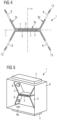
- the Figure 5 shows a perspective view of a possible contacting of the electronic component according to Figure 4 .
- the component 1 is placed in a housing 6.
- the housing 6 is frame-shaped.
- the component 1 is contacted (screwed, clamped, or similar) through the housing 6 by means of an insulated, flexible copper cable (not explicitly shown).
- the contacting is carried out as in connection with the Figure 2 described via the nuts 10, the threaded rod 11, which is inserted into the recess 8 of the respective contact element 3, as well as the electrically conductive connection of the contact elements 3 with cable lugs into which the copper cables are inserted.
- the copper cables are inserted into the housing 6 via recesses 6a on a top and bottom side of the housing 6.
- the housing 6 has a mechanical strain relief 4 for the copper cables.
- the strain relief 4 can be arranged, for example, on a top side and a bottom side 4 of the housing 6. When mechanical tension is applied to the copper cables, the strain relief 4 ensures that no or only minimal forces act on the component 1 and, in particular, the connecting material 7. The component 1 is therefore preferably held stress-free by the strain relief 4.
- the Figure 6 shows a schematic sectional view of an electronic component according to a further embodiment.
- component 1 corresponds to component 1 from Figure 4
- the contact elements 3 are not arranged mirror-symmetrically to the longitudinal axis L. Rather, the contact elements 3 are offset from each other by 90°. This allows for different installation situations to be accommodated.
- the Figure 7 shows a perspective view of an electronic component according to a further embodiment.
- component 1 corresponds to component 1 from Figure 6
- the component 1 according to Figure 7 several NTC elements 2 and several contact elements 3.
- the component 1 can have up to ten NTC elements 2, each of which is round or disc-shaped and electrically connected in parallel.
- the contact elements 3 are arranged between the NTC elements 2.
- the component 1 thus has, as already described in connection with the Figure 3 described a layer sequence of alternatingly arranged NTC elements 2 and contact elements 3.
- FIG 8 shows a schematic sectional view of an electronic component according to a further embodiment.
- Figure 9 further shows a plan view of a portion of the electronic component according to Figure 8 .
- NTC element 2 In contrast to the embodiment according to the Figure 1 An NTC element 2 is used, which has been divided or segmented into smaller NTC elements or segments 2a by sawing or scoring.
- the NTC element 2 has a plurality of segments 2a.
- the NTC element 2 has, unlike in Figure 1 preferably a rectangular shape.
- the NTC element 2 has a width and a height of less than or equal to 13 mm, for example 12.7 mm.
- the respective segment 2a is also preferably rectangular.
- the respective segment 2a has a length and a width of approximately 2 mm each.
- the contact elements 3 should also be rectangular for this design.
- the respective contact element is Figures 8 and 9 formed from three rectangular sub-areas 3a, 3b, 3c.
- the three sub-areas preferably have the same length, for example 15 mm.
- the expansion joints 15 have a width of 0.05 mm to 0.2 mm, for example, 0.1 mm. These expansion joints 15 reduce thermal stresses in the NTC element 2 during normal operation.
- ceramic multilayer technology is suitable, in which an NTC substrate made of stacked ceramic foils is segmented before or after metallization by so-called "dicing". All other features correspond to those associated with the Figure 1 described characteristics.
- FIG. 10 shows a schematic sectional view of an electronic component according to a further embodiment.
- Figure 11 shows a plan view of a portion of the electronic component according to the Figure 10 .
- This embodiment combines features of the embodiments according to the Figures 4 and 8 and 9.
- the NTC element 2 is - as described in connection with the Figures 8 and 9 described - separated into individual segments 2a. All other characteristics correspond to those described in connection with the Figures 4 , 8 and 9 described characteristics.
- FIG. 12 shows a schematic sectional view of an electronic component according to a further embodiment.
- Figure 13 shows a perspective view of a portion of the electronic component according to Figure 12 .
- the contact elements 3 are as in connection with Figure 4 As described, it is double-sided.
- the NTC element 2 is arranged between the first partial area 3a of the contact elements 3 and is electrically and thermally connected to the contact elements 3 via the connecting material 7.
- the screw connection is in contrast to the screw connection according to Figure 2 insulating
- the NTC element 2 is designed in a ring shape.
- the NTC element 2 has a round, continuous recess.
- the first partial area 3a of the respective contact element 3 also has a recess in this exemplary embodiment.
- the recesses of the contact elements 3 and the NTC element 2 are designed and arranged to enable the insulating screw connection of the contact elements 3.
- the recesses are provided for the introduction of a threaded rod 11 for screwing the contact elements 3.
- a spacer 9 is arranged, which has a recess 9a ( Figure 13 ).
- the respective spacer is, for example, a PTFE disk.
- the respective spacer has, for example, a diameter of 15 mm.
- a spacer 9 is arranged on an upper side of the first partial area 3a of the first or upper contact element 3.
- Another spacer 9 is arranged on an underside of the first partial area 3a of the second or lower contact element 3.
- a nut 10 is arranged on each of the spacers 9. The threaded rod 11 is guided through the nuts 10, the recesses in the spacers 9, the NTC element 2 and the contact elements 3 for screwing the contact elements 3.
- An insulating element 14 is introduced into the recess of the NTC element 2 between the threaded rod 11 and the NTC element 2.
- the insulating element 14 can, for example, comprise AlO x .
- the insulating element 14 is an AlO x tube. This enables an insulating screw connection of component 1.
- the electrical contacting of component 1 is again carried out as in connection with the Figure 2 described via the electrically conductive connection of the contact elements 3 with the battery cables via the cable lugs 5.
- the cable lugs are screwed to the contact elements 3 via the recesses 8 of the contact elements 3.
Landscapes
- Engineering & Computer Science (AREA)
- Microelectronics & Electronic Packaging (AREA)
- Physics & Mathematics (AREA)
- Electromagnetism (AREA)
- Manufacturing & Machinery (AREA)
- Thermistors And Varistors (AREA)
- Details Of Resistors (AREA)
- Emergency Protection Circuit Devices (AREA)
- Powder Metallurgy (AREA)
Claims (17)
- Composant électronique (1) destiné à limiter le courant de mise en circuit, comprenant- au moins un élément CTN (2),- au moins deux éléments de contact (3) électriquement conducteurs,l'élément CTN (2) étant relié de manière électriquement conductrice à l'élément de contact (3) respectif par le biais d'un matériau de liaison (7) et le coefficient de dilatation thermique de l'élément de contact (3) respectif étant adapté au coefficient de dilatation thermique de l'élément CTN (2).caractérisé en ce quel'élément CTN (2) présente la composition La(1-x)EA(x)Mn(1-a-b-c)Fe(a)Co(b)Ni(c)O(3±δ),où 0 ≤ x ≤ 0,5 et 0 ≤ (a+b+c) ≤ 0,5 et où EA désigne un élément alcalino-terreux et δ un écart par rapport à un rapport stœchiométrique d'oxygène, l'élément alcalino-terreux (EA) étant choisi parmi le magnésium, le calcium, le strontium ou le baryum et/ou où |δ| ≤ 0,5.
- Composant électronique (1) selon la revendication 1,
l'élément CTN (2) possédant un côté supérieur et un côté inférieur, et le côté supérieur et le côté inférieur étant en contact électriquement conducteur au moins partiellement par le biais de l'élément de contact (3) respectif. - Composant électronique (1) selon la revendication 1 ou 2,
l'élément de contact (3) présentant un composé de matériau. - Composant électronique (1) selon l'une des revendications précédentes,
l'élément de contact (3) présentant du cuivre et l'élément de contact (3) présentant de l'invar ou du kovar. - Composant électronique (1) selon l'une des revendications précédentes,
l'élément de contact (3) présentant une structure stratifiée en cuivre - invar - cuivre avec un rapport d'épaisseur de 10 % ≤ cuivre 30 % -50 % ≤ invar / kovar ≤ 80 % - 10 % ≤ cuivre ≤ 30 %. - Composant électronique (1) selon l'une des revendications précédentes,
le matériau de liaison (7) présentant de l'argent fritté. - Composant électronique (1) selon l'une des revendications précédentes,
l'élément CTN (2) possédant deux, trois ou plus de segments (2a). - Composant électronique (1) selon l'une des revendications précédentes,
la résistance électrique spécifique de l'élément CTN (2) dans un état de base du composant électronique (1) étant ≤ 2 Ωcm. - Composant électronique (1) selon l'une des revendications précédentes,
l'élément de contact (3) présentant une épaisseur d, et 0,3 mm ≤ d ≤ 0,8 mm. - Composant électronique (1) selon l'une des revendications précédentes,
l'élément CTN (2) présentant une épaisseur d, et 100 µm ≤ d ≤ 600 µm. - Composant électronique (1) selon l'une des revendications précédentes,
possédant une pluralité d'éléments CTN (2) et d'éléments de contact (3), les éléments CTN (2) étant connectés en parallèle les uns avec les autres. - Composant électronique (1) selon la revendication 11,
les éléments CTN (2) étant disposés les uns au-dessus des autres en forme de pile, un élément de contact (3) étant respectivement disposé entre deux éléments CTN (2) voisins et les éléments CTN (2) étant couplés thermiquement les uns aux autres par le biais des éléments de contact (3). - Composant électronique (1) selon l'une des revendications précédentes,
l'élément CTN (2) présentant un coefficient de dilatation thermique compris entre 7 ppm/K et 10 ppm/K. - Composant électronique (1) selon l'une des revendications précédentes,
possédant un élément de fixation (10, 11), l'élément de fixation (10, 11) présentant une résistance électrique qui est égale ou seulement légèrement supérieure à la résistance de l'élément CTN (2) à des températures de fonctionnement basses. - Composant électronique (1) selon l'une des revendications précédentes,
l'élément CTN (2) présentant une résistance nominale R25 ≤ 1 Ω à une température de 25 °C. - Utilisation d'un composant électronique (1) selon l'une des revendications 1 à 15 pour des systèmes de démarrage/arrêt dans le secteur automobile.
- Utilisation d'un composant électronique (1) selon l'une des revendications 1 à 15 pour des courants jusqu'à 1000 A sous tension continue dans des réseaux de 12 V et 24 V.
Priority Applications (1)
| Application Number | Priority Date | Filing Date | Title |
|---|---|---|---|
| EP25169735.5A EP4560654A3 (fr) | 2016-04-28 | 2017-04-18 | Composant électronique pour limiter le courant de démarrage et utilisation d'un composant électronique |
Applications Claiming Priority (2)
| Application Number | Priority Date | Filing Date | Title |
|---|---|---|---|
| DE102016107931.6A DE102016107931B4 (de) | 2016-04-28 | 2016-04-28 | Elektronisches Bauelement zur Einschaltstrombegrenzung und Verwendung eines elektronischen Bauelements |
| PCT/EP2017/059132 WO2017186527A1 (fr) | 2016-04-28 | 2017-04-18 | Composant électronique destiné à la limitation d'un courant de mise sous tension et utilisation d'un composant électronique |
Related Child Applications (2)
| Application Number | Title | Priority Date | Filing Date |
|---|---|---|---|
| EP25169735.5A Division EP4560654A3 (fr) | 2016-04-28 | 2017-04-18 | Composant électronique pour limiter le courant de démarrage et utilisation d'un composant électronique |
| EP25169735.5A Division-Into EP4560654A3 (fr) | 2016-04-28 | 2017-04-18 | Composant électronique pour limiter le courant de démarrage et utilisation d'un composant électronique |
Publications (2)
| Publication Number | Publication Date |
|---|---|
| EP3449490A1 EP3449490A1 (fr) | 2019-03-06 |
| EP3449490B1 true EP3449490B1 (fr) | 2025-06-25 |
Family
ID=58668845
Family Applications (2)
| Application Number | Title | Priority Date | Filing Date |
|---|---|---|---|
| EP25169735.5A Pending EP4560654A3 (fr) | 2016-04-28 | 2017-04-18 | Composant électronique pour limiter le courant de démarrage et utilisation d'un composant électronique |
| EP17721065.5A Active EP3449490B1 (fr) | 2016-04-28 | 2017-04-18 | Composant électronique destiné à la limitation d'un courant de mise sous tension et utilisation d'un composant électronique |
Family Applications Before (1)
| Application Number | Title | Priority Date | Filing Date |
|---|---|---|---|
| EP25169735.5A Pending EP4560654A3 (fr) | 2016-04-28 | 2017-04-18 | Composant électronique pour limiter le courant de démarrage et utilisation d'un composant électronique |
Country Status (7)
| Country | Link |
|---|---|
| US (1) | US11289244B2 (fr) |
| EP (2) | EP4560654A3 (fr) |
| JP (2) | JP2019523980A (fr) |
| KR (1) | KR20180136944A (fr) |
| CN (2) | CN109074923A (fr) |
| DE (1) | DE102016107931B4 (fr) |
| WO (1) | WO2017186527A1 (fr) |
Families Citing this family (4)
| Publication number | Priority date | Publication date | Assignee | Title |
|---|---|---|---|---|
| DE102017215233A1 (de) * | 2017-08-31 | 2019-02-28 | Seg Automotive Germany Gmbh | NTC-Bauteil zum Einbau in den Stromkreis einer elektrischen Baueinheit |
| DE102018104459A1 (de) | 2018-02-27 | 2019-08-29 | Tdk Electronics Ag | Vielschichtbauelement mit externer Kontaktierung |
| CN110698189B (zh) * | 2019-11-15 | 2021-11-02 | 中国科学院新疆理化技术研究所 | 一种镧离子掺杂的深低温热敏电阻材料及制备方法 |
| CN114029493B (zh) * | 2021-09-16 | 2024-01-09 | 清华大学深圳国际研究生院 | 一种与ZnO-V2O5系压敏电阻共烧的纯银内电极及其制备方法与应用 |
Citations (1)
| Publication number | Priority date | Publication date | Assignee | Title |
|---|---|---|---|---|
| WO2015181014A1 (fr) * | 2014-05-27 | 2015-12-03 | Epcos Ag | Composant électronique |
Family Cites Families (36)
| Publication number | Priority date | Publication date | Assignee | Title |
|---|---|---|---|---|
| DE620678C (de) * | 1933-05-23 | 1935-10-26 | Patra Patent Treuhand | Elektrische Widerstandsanordnung aus parallel geschalteten Widerstaenden mit hohem negativem Temperaturkoeffizienten |
| NL77388C (fr) * | 1949-02-08 | 1955-02-15 | ||
| FR1332617A (fr) * | 1962-06-02 | 1963-07-19 | Perfectionnements aux procédés de fabrication de résistances électriques et aux résistances fabriquées selon ces procédés | |
| US3358362A (en) * | 1965-01-21 | 1967-12-19 | Int Resistance Co | Method of making an electrical resistor |
| US3435399A (en) | 1966-04-19 | 1969-03-25 | Gen Electric | Thermistor device and method of producing said device |
| US4447799A (en) * | 1981-01-30 | 1984-05-08 | General Electric Company | High temperature thermistor and method of assembling the same |
| JPS63138705A (ja) * | 1986-12-01 | 1988-06-10 | ティーディーケイ株式会社 | サ−ミスタ素子およびその製造方法 |
| JP2643396B2 (ja) * | 1988-12-15 | 1997-08-20 | 日立電線株式会社 | セラミックコンデンサに半田接合される板状のリード線 |
| JPH0470701U (fr) * | 1990-10-30 | 1992-06-23 | ||
| JPH0729667A (ja) | 1993-07-08 | 1995-01-31 | Mitsubishi Materials Corp | 放電型サージアブソーバ及びその製造方法 |
| JP3346239B2 (ja) * | 1997-09-19 | 2002-11-18 | 株式会社村田製作所 | 電子部品の製造方法 |
| JPH11135304A (ja) * | 1997-10-27 | 1999-05-21 | Murata Mfg Co Ltd | Ntcサーミスタ及び電流制限回路 |
| JPH11340007A (ja) * | 1998-05-22 | 1999-12-10 | Murata Mfg Co Ltd | 負特性サーミスタおよび電子複写機 |
| US6081416A (en) | 1998-05-28 | 2000-06-27 | Trinh; Hung | Lead frames for mounting ceramic electronic parts, particularly ceramic capacitors, where the coefficient of thermal expansion of the lead frame is less than that of the ceramic |
| JP3801872B2 (ja) * | 2001-03-05 | 2006-07-26 | 株式会社日立製作所 | 抵抗体素子および熱式流体測定計 |
| DE10317466A1 (de) * | 2003-04-16 | 2004-12-09 | Robert Bosch Gmbh | Elektromotor |
| JP5059332B2 (ja) * | 2006-02-16 | 2012-10-24 | 日本特殊陶業株式会社 | サーミスタ素子、これを用いた温度センサ、及びサーミスタ素子の製造方法 |
| KR100732878B1 (ko) * | 2006-03-02 | 2007-07-02 | (주)성음하이텍 | 서미스터 온도 감지 회로를 장착한 사운드(보이스) 컵 |
| DE102006053085A1 (de) * | 2006-11-10 | 2008-05-15 | Epcos Ag | Elektrische Baugruppe mit PTC-Widerstandselementen |
| DE102006060387A1 (de) * | 2006-12-20 | 2008-06-26 | Isabellenhütte Heusler Gmbh & Co. Kg | Widerstand, insbesondere SMD-Widerstand, und zugehöriges Herstellungsverfahren |
| CN101765569B (zh) * | 2007-08-22 | 2012-11-28 | 株式会社村田制作所 | 半导体陶瓷材料及ntc热敏电阻 |
| US8228160B2 (en) * | 2008-11-14 | 2012-07-24 | Epcos Ag | Sensor element and process for assembling a sensor element |
| JP5346867B2 (ja) * | 2010-04-09 | 2013-11-20 | 日本特殊陶業株式会社 | サーミスタ素子及び温度センサ |
| JP5304822B2 (ja) * | 2010-04-28 | 2013-10-02 | 株式会社デンソー | 温度センサ |
| KR101471829B1 (ko) * | 2010-06-24 | 2014-12-24 | 티디케이가부시기가이샤 | 칩 서미스터 및 그 제조 방법 |
| DE102010053389A1 (de) * | 2010-12-03 | 2012-06-06 | Vishay Electronic Gmbh | Elektrischer Leistungswiderstand |
| JP5885027B2 (ja) * | 2012-03-16 | 2016-03-15 | 三菱マテリアル株式会社 | サーミスタ素子 |
| DE102012109704A1 (de) * | 2012-10-11 | 2014-04-17 | Epcos Ag | Keramisches Bauelement mit Schutzschicht und Verfahren zu dessen Herstellung |
| CN103066662B (zh) * | 2013-01-07 | 2015-08-05 | 雷星亮 | 应急电源 |
| JP2015111652A (ja) * | 2013-10-31 | 2015-06-18 | 株式会社村田製作所 | 電子部品 |
| DE202013009973U1 (de) * | 2013-11-04 | 2013-11-20 | Isabellenhütte Heusler Gmbh & Co. Kg | Widerstand, insbesondere niederohmiger Strommesswiderstand |
| JP2015160224A (ja) * | 2014-02-27 | 2015-09-07 | 日立金属株式会社 | 接合用材料 |
| KR101646711B1 (ko) * | 2014-04-25 | 2016-08-09 | (주) 래트론 | 온도 센서 소자 및 그 제조 방법 |
| DE102015102866B4 (de) | 2015-02-27 | 2023-02-02 | Tdk Electronics Ag | Keramisches Bauelement, Bauelementanordnung und Verfahren zur Herstellung eines keramischen Bauelements |
| CN105006317A (zh) * | 2015-08-03 | 2015-10-28 | 成都顺康电子有限责任公司 | 一种玻璃封装ptc热敏电阻及其制作方法 |
| DE102015121982A1 (de) | 2015-12-16 | 2017-06-22 | Epcos Ag | NTC-Keramik, elektronisches Bauelement zur Einschaltstrombegrenzung und Verfahren zur Herstellung eines elektronischen Bauelements |
-
2016
- 2016-04-28 DE DE102016107931.6A patent/DE102016107931B4/de active Active
-
2017
- 2017-04-18 US US16/090,805 patent/US11289244B2/en active Active
- 2017-04-18 CN CN201780026076.3A patent/CN109074923A/zh active Pending
- 2017-04-18 EP EP25169735.5A patent/EP4560654A3/fr active Pending
- 2017-04-18 KR KR1020187028851A patent/KR20180136944A/ko not_active Ceased
- 2017-04-18 EP EP17721065.5A patent/EP3449490B1/fr active Active
- 2017-04-18 CN CN202111490705.2A patent/CN114156027B/zh active Active
- 2017-04-18 WO PCT/EP2017/059132 patent/WO2017186527A1/fr not_active Ceased
- 2017-04-18 JP JP2018554544A patent/JP2019523980A/ja active Pending
-
2020
- 2020-09-24 JP JP2020160004A patent/JP7186753B2/ja active Active
Patent Citations (1)
| Publication number | Priority date | Publication date | Assignee | Title |
|---|---|---|---|---|
| WO2015181014A1 (fr) * | 2014-05-27 | 2015-12-03 | Epcos Ag | Composant électronique |
Also Published As
| Publication number | Publication date |
|---|---|
| EP3449490A1 (fr) | 2019-03-06 |
| EP4560654A3 (fr) | 2025-07-30 |
| DE102016107931B4 (de) | 2026-01-22 |
| US11289244B2 (en) | 2022-03-29 |
| JP2021010014A (ja) | 2021-01-28 |
| EP4560654A2 (fr) | 2025-05-28 |
| DE102016107931A1 (de) | 2017-11-02 |
| JP2019523980A (ja) | 2019-08-29 |
| KR20180136944A (ko) | 2018-12-26 |
| WO2017186527A1 (fr) | 2017-11-02 |
| CN114156027A (zh) | 2022-03-08 |
| CN114156027B (zh) | 2024-10-01 |
| CN109074923A (zh) | 2018-12-21 |
| US20200118718A1 (en) | 2020-04-16 |
| JP7186753B2 (ja) | 2022-12-09 |
Similar Documents
| Publication | Publication Date | Title |
|---|---|---|
| EP0576836B1 (fr) | Dispositif limitant le courant | |
| EP3449490B1 (fr) | Composant électronique destiné à la limitation d'un courant de mise sous tension et utilisation d'un composant électronique | |
| DE4142523A1 (de) | Widerstand mit ptc - verhalten | |
| EP2917712B1 (fr) | Capteur de température et procede de production d'un capteur de température | |
| DE102019111384B3 (de) | Piezoelektrische Sende- und/oder Empfangseinrichtung und Vibrationsgrenzstandsensor mit einer solchen | |
| DE102015121982A1 (de) | NTC-Keramik, elektronisches Bauelement zur Einschaltstrombegrenzung und Verfahren zur Herstellung eines elektronischen Bauelements | |
| WO2012025476A1 (fr) | Élément semiconducteur et matériau d'isolation annulaire pour un module thermoélectrique | |
| EP1355327B1 (fr) | Limiteur de surtension et méthode de fabrication d' un tel limiteur de surtension | |
| EP2732452B1 (fr) | Dispositif electrique | |
| DE19814697C1 (de) | Piezoelektrischer Aktor und Verfahren zu seiner Herstellung | |
| EP0057172B1 (fr) | Elément chauffant auto-régulateur | |
| EP1774603B1 (fr) | Dispositif multicouche et procede pour sa production | |
| EP3149748B1 (fr) | Systeme comprenant élément ctn et consommateur électrique connectés en série | |
| EP2529423B1 (fr) | Composant piézoélectrique | |
| EP3033756A1 (fr) | Composant multicouche comportant un élément de mise en contact extérieur et procédé de fabrication d'un composant multicouche comportant un élément de mise en contact extérieur | |
| DE102004004737A1 (de) | Piezoaktor und ein Verfahren zu dessen Herstellung | |
| EP3959752B1 (fr) | Actionneur électromécanique à isolation céramique et son procédé de fabrication | |
| EP3682509B1 (fr) | Interface de contact électrique ayant une résistance de contact électrique faible et stable | |
| DE19951016A1 (de) | Piezoelektrischer Keramikkörper | |
| WO2013098168A1 (fr) | Pile piézo-électrique avec et procédé de passivation d'une pile piézo-électrique | |
| EP4581900A1 (fr) | Élément céramique fonctionnel monolithique et procédé d'établissement d'une connexion par contact pour une céramique fonctionnelle | |
| EP1231613A1 (fr) | Eléments résistifs avec comportement PTC | |
| DE9217269U1 (de) | Elektrischer Leistungswiderstand |
Legal Events
| Date | Code | Title | Description |
|---|---|---|---|
| STAA | Information on the status of an ep patent application or granted ep patent |
Free format text: STATUS: UNKNOWN |
|
| STAA | Information on the status of an ep patent application or granted ep patent |
Free format text: STATUS: THE INTERNATIONAL PUBLICATION HAS BEEN MADE |
|
| PUAI | Public reference made under article 153(3) epc to a published international application that has entered the european phase |
Free format text: ORIGINAL CODE: 0009012 |
|
| STAA | Information on the status of an ep patent application or granted ep patent |
Free format text: STATUS: REQUEST FOR EXAMINATION WAS MADE |
|
| 17P | Request for examination filed |
Effective date: 20180906 |
|
| AK | Designated contracting states |
Kind code of ref document: A1 Designated state(s): AL AT BE BG CH CY CZ DE DK EE ES FI FR GB GR HR HU IE IS IT LI LT LU LV MC MK MT NL NO PL PT RO RS SE SI SK SM TR |
|
| AX | Request for extension of the european patent |
Extension state: BA ME |
|
| DAV | Request for validation of the european patent (deleted) | ||
| DAX | Request for extension of the european patent (deleted) | ||
| RIN1 | Information on inventor provided before grant (corrected) |
Inventor name: HOFRICHTER, ALFRED Inventor name: RINNER, FRANZ Inventor name: WISCHNAT, VOLKER |
|
| STAA | Information on the status of an ep patent application or granted ep patent |
Free format text: STATUS: EXAMINATION IS IN PROGRESS |
|
| 17Q | First examination report despatched |
Effective date: 20210817 |
|
| GRAP | Despatch of communication of intention to grant a patent |
Free format text: ORIGINAL CODE: EPIDOSNIGR1 |
|
| STAA | Information on the status of an ep patent application or granted ep patent |
Free format text: STATUS: GRANT OF PATENT IS INTENDED |
|
| INTG | Intention to grant announced |
Effective date: 20250227 |
|
| GRAS | Grant fee paid |
Free format text: ORIGINAL CODE: EPIDOSNIGR3 |
|
| GRAA | (expected) grant |
Free format text: ORIGINAL CODE: 0009210 |
|
| STAA | Information on the status of an ep patent application or granted ep patent |
Free format text: STATUS: THE PATENT HAS BEEN GRANTED |
|
| AK | Designated contracting states |
Kind code of ref document: B1 Designated state(s): AL AT BE BG CH CY CZ DE DK EE ES FI FR GB GR HR HU IE IS IT LI LT LU LV MC MK MT NL NO PL PT RO RS SE SI SK SM TR |
|
| REG | Reference to a national code |
Ref country code: GB Ref legal event code: FG4D Free format text: NOT ENGLISH |
|
| REG | Reference to a national code |
Ref country code: CH Ref legal event code: EP |
|
| REG | Reference to a national code |
Ref country code: CH Ref legal event code: EP |
|
| REG | Reference to a national code |
Ref country code: IE Ref legal event code: FG4D Free format text: LANGUAGE OF EP DOCUMENT: GERMAN |
|
| REG | Reference to a national code |
Ref country code: DE Ref legal event code: R096 Ref document number: 502017016925 Country of ref document: DE |
|
| PG25 | Lapsed in a contracting state [announced via postgrant information from national office to epo] |
Ref country code: FI Free format text: LAPSE BECAUSE OF FAILURE TO SUBMIT A TRANSLATION OF THE DESCRIPTION OR TO PAY THE FEE WITHIN THE PRESCRIBED TIME-LIMIT Effective date: 20250625 |
|
| REG | Reference to a national code |
Ref country code: LT Ref legal event code: MG9D |
|
| PG25 | Lapsed in a contracting state [announced via postgrant information from national office to epo] |
Ref country code: GR Free format text: LAPSE BECAUSE OF FAILURE TO SUBMIT A TRANSLATION OF THE DESCRIPTION OR TO PAY THE FEE WITHIN THE PRESCRIBED TIME-LIMIT Effective date: 20250926 Ref country code: NO Free format text: LAPSE BECAUSE OF FAILURE TO SUBMIT A TRANSLATION OF THE DESCRIPTION OR TO PAY THE FEE WITHIN THE PRESCRIBED TIME-LIMIT Effective date: 20250925 |
|
| PG25 | Lapsed in a contracting state [announced via postgrant information from national office to epo] |
Ref country code: BG Free format text: LAPSE BECAUSE OF FAILURE TO SUBMIT A TRANSLATION OF THE DESCRIPTION OR TO PAY THE FEE WITHIN THE PRESCRIBED TIME-LIMIT Effective date: 20250625 |
|
| PG25 | Lapsed in a contracting state [announced via postgrant information from national office to epo] |
Ref country code: HR Free format text: LAPSE BECAUSE OF FAILURE TO SUBMIT A TRANSLATION OF THE DESCRIPTION OR TO PAY THE FEE WITHIN THE PRESCRIBED TIME-LIMIT Effective date: 20250625 |
|
| PG25 | Lapsed in a contracting state [announced via postgrant information from national office to epo] |
Ref country code: RS Free format text: LAPSE BECAUSE OF FAILURE TO SUBMIT A TRANSLATION OF THE DESCRIPTION OR TO PAY THE FEE WITHIN THE PRESCRIBED TIME-LIMIT Effective date: 20250925 |
|
| PG25 | Lapsed in a contracting state [announced via postgrant information from national office to epo] |
Ref country code: LV Free format text: LAPSE BECAUSE OF FAILURE TO SUBMIT A TRANSLATION OF THE DESCRIPTION OR TO PAY THE FEE WITHIN THE PRESCRIBED TIME-LIMIT Effective date: 20250625 |
|
| REG | Reference to a national code |
Ref country code: NL Ref legal event code: MP Effective date: 20250625 |
|
| PG25 | Lapsed in a contracting state [announced via postgrant information from national office to epo] |
Ref country code: NL Free format text: LAPSE BECAUSE OF FAILURE TO SUBMIT A TRANSLATION OF THE DESCRIPTION OR TO PAY THE FEE WITHIN THE PRESCRIBED TIME-LIMIT Effective date: 20250625 |
|
| PG25 | Lapsed in a contracting state [announced via postgrant information from national office to epo] |
Ref country code: PT Free format text: LAPSE BECAUSE OF FAILURE TO SUBMIT A TRANSLATION OF THE DESCRIPTION OR TO PAY THE FEE WITHIN THE PRESCRIBED TIME-LIMIT Effective date: 20251027 |
|
| PG25 | Lapsed in a contracting state [announced via postgrant information from national office to epo] |
Ref country code: IS Free format text: LAPSE BECAUSE OF FAILURE TO SUBMIT A TRANSLATION OF THE DESCRIPTION OR TO PAY THE FEE WITHIN THE PRESCRIBED TIME-LIMIT Effective date: 20251025 |
|
| PG25 | Lapsed in a contracting state [announced via postgrant information from national office to epo] |
Ref country code: SM Free format text: LAPSE BECAUSE OF FAILURE TO SUBMIT A TRANSLATION OF THE DESCRIPTION OR TO PAY THE FEE WITHIN THE PRESCRIBED TIME-LIMIT Effective date: 20250625 |
|
| PG25 | Lapsed in a contracting state [announced via postgrant information from national office to epo] |
Ref country code: CZ Free format text: LAPSE BECAUSE OF FAILURE TO SUBMIT A TRANSLATION OF THE DESCRIPTION OR TO PAY THE FEE WITHIN THE PRESCRIBED TIME-LIMIT Effective date: 20250625 |
|
| PG25 | Lapsed in a contracting state [announced via postgrant information from national office to epo] |
Ref country code: PL Free format text: LAPSE BECAUSE OF FAILURE TO SUBMIT A TRANSLATION OF THE DESCRIPTION OR TO PAY THE FEE WITHIN THE PRESCRIBED TIME-LIMIT Effective date: 20250625 |
|
| PG25 | Lapsed in a contracting state [announced via postgrant information from national office to epo] |
Ref country code: EE Free format text: LAPSE BECAUSE OF FAILURE TO SUBMIT A TRANSLATION OF THE DESCRIPTION OR TO PAY THE FEE WITHIN THE PRESCRIBED TIME-LIMIT Effective date: 20250625 |
|
| PG25 | Lapsed in a contracting state [announced via postgrant information from national office to epo] |
Ref country code: SK Free format text: LAPSE BECAUSE OF FAILURE TO SUBMIT A TRANSLATION OF THE DESCRIPTION OR TO PAY THE FEE WITHIN THE PRESCRIBED TIME-LIMIT Effective date: 20250625 Ref country code: RO Free format text: LAPSE BECAUSE OF FAILURE TO SUBMIT A TRANSLATION OF THE DESCRIPTION OR TO PAY THE FEE WITHIN THE PRESCRIBED TIME-LIMIT Effective date: 20250625 |
|
| PG25 | Lapsed in a contracting state [announced via postgrant information from national office to epo] |
Ref country code: ES Free format text: LAPSE BECAUSE OF FAILURE TO SUBMIT A TRANSLATION OF THE DESCRIPTION OR TO PAY THE FEE WITHIN THE PRESCRIBED TIME-LIMIT Effective date: 20250625 |
|
| PG25 | Lapsed in a contracting state [announced via postgrant information from national office to epo] |
Ref country code: DK Free format text: LAPSE BECAUSE OF FAILURE TO SUBMIT A TRANSLATION OF THE DESCRIPTION OR TO PAY THE FEE WITHIN THE PRESCRIBED TIME-LIMIT Effective date: 20250625 |
|
| PG25 | Lapsed in a contracting state [announced via postgrant information from national office to epo] |
Ref country code: IT Free format text: LAPSE BECAUSE OF FAILURE TO SUBMIT A TRANSLATION OF THE DESCRIPTION OR TO PAY THE FEE WITHIN THE PRESCRIBED TIME-LIMIT Effective date: 20250625 |
|
| PLBE | No opposition filed within time limit |
Free format text: ORIGINAL CODE: 0009261 |
|
| STAA | Information on the status of an ep patent application or granted ep patent |
Free format text: STATUS: NO OPPOSITION FILED WITHIN TIME LIMIT |