EP3509089A1 - Procédé de nettoyage de chambre de production de semi-conducteur - Google Patents
Procédé de nettoyage de chambre de production de semi-conducteur Download PDFInfo
- Publication number
- EP3509089A1 EP3509089A1 EP17846451.7A EP17846451A EP3509089A1 EP 3509089 A1 EP3509089 A1 EP 3509089A1 EP 17846451 A EP17846451 A EP 17846451A EP 3509089 A1 EP3509089 A1 EP 3509089A1
- Authority
- EP
- European Patent Office
- Prior art keywords
- chamber
- temperature
- chlorine trifluoride
- exhaust tube
- gas
- Prior art date
- Legal status (The legal status is an assumption and is not a legal conclusion. Google has not performed a legal analysis and makes no representation as to the accuracy of the status listed.)
- Withdrawn
Links
Images
Classifications
-
- H—ELECTRICITY
- H10—SEMICONDUCTOR DEVICES; ELECTRIC SOLID-STATE DEVICES NOT OTHERWISE PROVIDED FOR
- H10P—GENERIC PROCESSES OR APPARATUS FOR THE MANUFACTURE OR TREATMENT OF DEVICES COVERED BY CLASS H10
- H10P70/00—Cleaning of wafers, substrates or parts of devices
-
- C—CHEMISTRY; METALLURGY
- C23—COATING METALLIC MATERIAL; COATING MATERIAL WITH METALLIC MATERIAL; CHEMICAL SURFACE TREATMENT; DIFFUSION TREATMENT OF METALLIC MATERIAL; COATING BY VACUUM EVAPORATION, BY SPUTTERING, BY ION IMPLANTATION OR BY CHEMICAL VAPOUR DEPOSITION, IN GENERAL; INHIBITING CORROSION OF METALLIC MATERIAL OR INCRUSTATION IN GENERAL
- C23C—COATING METALLIC MATERIAL; COATING MATERIAL WITH METALLIC MATERIAL; SURFACE TREATMENT OF METALLIC MATERIAL BY DIFFUSION INTO THE SURFACE, BY CHEMICAL CONVERSION OR SUBSTITUTION; COATING BY VACUUM EVAPORATION, BY SPUTTERING, BY ION IMPLANTATION OR BY CHEMICAL VAPOUR DEPOSITION, IN GENERAL
- C23C16/00—Chemical coating by decomposition of gaseous compounds, without leaving reaction products of surface material in the coating, i.e. chemical vapour deposition [CVD] processes
- C23C16/44—Chemical coating by decomposition of gaseous compounds, without leaving reaction products of surface material in the coating, i.e. chemical vapour deposition [CVD] processes characterised by the method of coating
- C23C16/4401—Means for minimising impurities, e.g. dust, moisture or residual gas, in the reaction chamber
- C23C16/4405—Cleaning of reactor or parts inside the reactor by using reactive gases
-
- B—PERFORMING OPERATIONS; TRANSPORTING
- B08—CLEANING
- B08B—CLEANING IN GENERAL; PREVENTION OF FOULING IN GENERAL
- B08B13/00—Accessories or details of general applicability for machines or apparatus for cleaning
-
- B—PERFORMING OPERATIONS; TRANSPORTING
- B08—CLEANING
- B08B—CLEANING IN GENERAL; PREVENTION OF FOULING IN GENERAL
- B08B5/00—Cleaning by methods involving the use of air flow or gas flow
-
- B—PERFORMING OPERATIONS; TRANSPORTING
- B08—CLEANING
- B08B—CLEANING IN GENERAL; PREVENTION OF FOULING IN GENERAL
- B08B9/00—Cleaning hollow articles by methods or apparatus specially adapted thereto
- B08B9/02—Cleaning pipes or tubes or systems of pipes or tubes
- B08B9/027—Cleaning the internal surfaces; Removal of blockages
- B08B9/032—Cleaning the internal surfaces; Removal of blockages by the mechanical action of a moving fluid, e.g. by flushing
-
- B—PERFORMING OPERATIONS; TRANSPORTING
- B08—CLEANING
- B08B—CLEANING IN GENERAL; PREVENTION OF FOULING IN GENERAL
- B08B9/00—Cleaning hollow articles by methods or apparatus specially adapted thereto
- B08B9/08—Cleaning containers, e.g. tanks
-
- C—CHEMISTRY; METALLURGY
- C23—COATING METALLIC MATERIAL; COATING MATERIAL WITH METALLIC MATERIAL; CHEMICAL SURFACE TREATMENT; DIFFUSION TREATMENT OF METALLIC MATERIAL; COATING BY VACUUM EVAPORATION, BY SPUTTERING, BY ION IMPLANTATION OR BY CHEMICAL VAPOUR DEPOSITION, IN GENERAL; INHIBITING CORROSION OF METALLIC MATERIAL OR INCRUSTATION IN GENERAL
- C23C—COATING METALLIC MATERIAL; COATING MATERIAL WITH METALLIC MATERIAL; SURFACE TREATMENT OF METALLIC MATERIAL BY DIFFUSION INTO THE SURFACE, BY CHEMICAL CONVERSION OR SUBSTITUTION; COATING BY VACUUM EVAPORATION, BY SPUTTERING, BY ION IMPLANTATION OR BY CHEMICAL VAPOUR DEPOSITION, IN GENERAL
- C23C16/00—Chemical coating by decomposition of gaseous compounds, without leaving reaction products of surface material in the coating, i.e. chemical vapour deposition [CVD] processes
- C23C16/22—Chemical coating by decomposition of gaseous compounds, without leaving reaction products of surface material in the coating, i.e. chemical vapour deposition [CVD] processes characterised by the deposition of inorganic material, other than metallic material
- C23C16/30—Deposition of compounds, mixtures or solid solutions, e.g. borides, carbides, nitrides
- C23C16/32—Carbides
- C23C16/325—Silicon carbide
-
- C—CHEMISTRY; METALLURGY
- C23—COATING METALLIC MATERIAL; COATING MATERIAL WITH METALLIC MATERIAL; CHEMICAL SURFACE TREATMENT; DIFFUSION TREATMENT OF METALLIC MATERIAL; COATING BY VACUUM EVAPORATION, BY SPUTTERING, BY ION IMPLANTATION OR BY CHEMICAL VAPOUR DEPOSITION, IN GENERAL; INHIBITING CORROSION OF METALLIC MATERIAL OR INCRUSTATION IN GENERAL
- C23C—COATING METALLIC MATERIAL; COATING MATERIAL WITH METALLIC MATERIAL; SURFACE TREATMENT OF METALLIC MATERIAL BY DIFFUSION INTO THE SURFACE, BY CHEMICAL CONVERSION OR SUBSTITUTION; COATING BY VACUUM EVAPORATION, BY SPUTTERING, BY ION IMPLANTATION OR BY CHEMICAL VAPOUR DEPOSITION, IN GENERAL
- C23C16/00—Chemical coating by decomposition of gaseous compounds, without leaving reaction products of surface material in the coating, i.e. chemical vapour deposition [CVD] processes
- C23C16/44—Chemical coating by decomposition of gaseous compounds, without leaving reaction products of surface material in the coating, i.e. chemical vapour deposition [CVD] processes characterised by the method of coating
- C23C16/4412—Details relating to the exhausts, e.g. pumps, filters, scrubbers, particle traps
-
- C—CHEMISTRY; METALLURGY
- C23—COATING METALLIC MATERIAL; COATING MATERIAL WITH METALLIC MATERIAL; CHEMICAL SURFACE TREATMENT; DIFFUSION TREATMENT OF METALLIC MATERIAL; COATING BY VACUUM EVAPORATION, BY SPUTTERING, BY ION IMPLANTATION OR BY CHEMICAL VAPOUR DEPOSITION, IN GENERAL; INHIBITING CORROSION OF METALLIC MATERIAL OR INCRUSTATION IN GENERAL
- C23C—COATING METALLIC MATERIAL; COATING MATERIAL WITH METALLIC MATERIAL; SURFACE TREATMENT OF METALLIC MATERIAL BY DIFFUSION INTO THE SURFACE, BY CHEMICAL CONVERSION OR SUBSTITUTION; COATING BY VACUUM EVAPORATION, BY SPUTTERING, BY ION IMPLANTATION OR BY CHEMICAL VAPOUR DEPOSITION, IN GENERAL
- C23C16/00—Chemical coating by decomposition of gaseous compounds, without leaving reaction products of surface material in the coating, i.e. chemical vapour deposition [CVD] processes
- C23C16/44—Chemical coating by decomposition of gaseous compounds, without leaving reaction products of surface material in the coating, i.e. chemical vapour deposition [CVD] processes characterised by the method of coating
- C23C16/46—Chemical coating by decomposition of gaseous compounds, without leaving reaction products of surface material in the coating, i.e. chemical vapour deposition [CVD] processes characterised by the method of coating characterised by the method used for heating the substrate
-
- H—ELECTRICITY
- H10—SEMICONDUCTOR DEVICES; ELECTRIC SOLID-STATE DEVICES NOT OTHERWISE PROVIDED FOR
- H10P—GENERIC PROCESSES OR APPARATUS FOR THE MANUFACTURE OR TREATMENT OF DEVICES COVERED BY CLASS H10
- H10P72/00—Handling or holding of wafers, substrates or devices during manufacture or treatment thereof
- H10P72/04—Apparatus for manufacture or treatment
- H10P72/0402—Apparatus for fluid treatment
- H10P72/0406—Apparatus for fluid treatment for cleaning followed by drying, rinsing, stripping, blasting or the like
-
- H—ELECTRICITY
- H10—SEMICONDUCTOR DEVICES; ELECTRIC SOLID-STATE DEVICES NOT OTHERWISE PROVIDED FOR
- H10P—GENERIC PROCESSES OR APPARATUS FOR THE MANUFACTURE OR TREATMENT OF DEVICES COVERED BY CLASS H10
- H10P72/00—Handling or holding of wafers, substrates or devices during manufacture or treatment thereof
- H10P72/04—Apparatus for manufacture or treatment
- H10P72/0431—Apparatus for thermal treatment
-
- H—ELECTRICITY
- H10—SEMICONDUCTOR DEVICES; ELECTRIC SOLID-STATE DEVICES NOT OTHERWISE PROVIDED FOR
- H10P—GENERIC PROCESSES OR APPARATUS FOR THE MANUFACTURE OR TREATMENT OF DEVICES COVERED BY CLASS H10
- H10P72/00—Handling or holding of wafers, substrates or devices during manufacture or treatment thereof
- H10P72/06—Apparatus for monitoring, sorting, marking, testing or measuring
- H10P72/0602—Temperature monitoring
-
- B—PERFORMING OPERATIONS; TRANSPORTING
- B08—CLEANING
- B08B—CLEANING IN GENERAL; PREVENTION OF FOULING IN GENERAL
- B08B2209/00—Details of machines or methods for cleaning hollow articles
- B08B2209/02—Details of apparatuses or methods for cleaning pipes or tubes
- B08B2209/027—Details of apparatuses or methods for cleaning pipes or tubes for cleaning the internal surfaces
- B08B2209/032—Details of apparatuses or methods for cleaning pipes or tubes for cleaning the internal surfaces by the mechanical action of a moving fluid
-
- B—PERFORMING OPERATIONS; TRANSPORTING
- B08—CLEANING
- B08B—CLEANING IN GENERAL; PREVENTION OF FOULING IN GENERAL
- B08B2209/00—Details of machines or methods for cleaning hollow articles
- B08B2209/08—Details of machines or methods for cleaning containers, e.g. tanks
-
- H—ELECTRICITY
- H10—SEMICONDUCTOR DEVICES; ELECTRIC SOLID-STATE DEVICES NOT OTHERWISE PROVIDED FOR
- H10D—INORGANIC ELECTRIC SEMICONDUCTOR DEVICES
- H10D62/00—Semiconductor bodies, or regions thereof, of devices having potential barriers
- H10D62/80—Semiconductor bodies, or regions thereof, of devices having potential barriers characterised by the materials
- H10D62/83—Semiconductor bodies, or regions thereof, of devices having potential barriers characterised by the materials being Group IV materials, e.g. B-doped Si or undoped Ge
- H10D62/832—Semiconductor bodies, or regions thereof, of devices having potential barriers characterised by the materials being Group IV materials, e.g. B-doped Si or undoped Ge being Group IV materials comprising two or more elements, e.g. SiGe
- H10D62/8325—Silicon carbide
Definitions
- the present invention relates to a method for cleaning a semiconductor fabrication chamber.
- Gases known for use in gas cleaning include fluorine-containing gases used to remove the scale formed in the fabrication of semiconductors typified by Si or SiN x , such as chlorine trifluoride (ClF 3 ), nitrogen trifluoride (NF 3 ), carbon tetrafluoride (CF 4 ), and sulfur hexafluoride (SF 6 ). These gases provide cleaning performance in a plasma condition. Among them chlorine trifluoride attracts particular attention as a cleaning gas because it is capable of easily releasing fluorine atoms necessary for cleaning even in a non-plasma condition.
- Non-Patent Literature 1 proposes cleaning a SiC epitaxial reactor using chlorine trifluoride to remove SiC deposited on the surface of the susceptor. Patent Literature 1 below also discloses the same technique.
- Non-Patent Literature 2 reports the surface chemical condition of SiC after etching using chlorine trifluoride, suggesting that chlorine atoms and fluorine atoms originated in chlorine trifluoride remain after etching.
- Patent Literature 1 JP 2016-66658A
- Chlorine atoms or fluorine atoms remaining in a semiconductor fabrication chamber after cleaning the chamber using chlorine trifluoride can come to be mixed in a film formed in the chamber as impurities and deteriorate the film qualities. These residual atoms can also contribute to corrosion of jigs disposed in the chamber, such as a susceptor. This problem is particularly conspicuous when fluorine atoms remain in the chamber.
- An object of the present invention is to improve the method for cleaning a semiconductor fabrication chamber and, more particularly, to eliminate disadvantages associated with fluorine atoms remaining after cleaning.
- the present invention solves the above problem by the provision of a method for cleaning a semiconductor fabrication chamber comprising exposing the inside of the chamber after semiconductor fabrication to chlorine trifluoride to remove an object to be removed remaining in the chamber and thermally treating the inside of the chamber with at least one gas selected from the group consisting of nitrogen, argon, helium, and hydrogen.
- the present invention will be described on the basis of its preferred embodiments.
- the present invention relates to a method for cleaning a semiconductor fabrication chamber after semiconductor fabrication.
- semiconductor is used in its broadest sense to include various products composed of a semiconducting material, such as semiconductor wafers and semiconductor devices.
- the types of semiconductors are not particularly limited, and the cleaning method of the present invention is applicable to fabrication of a variety of semiconductors. Examples of semiconductors include Si, SiC, GaN, Ge, GaP, GaAs, ZnS, ZnSe, and diamond.
- the phrase "cleaning a semiconductor fabrication chamber” is intended to mean removing the scale deposited in the inside of the chamber and removing the scale deposited on the jigs disposed in the chamber.
- the jigs in the chamber typically include, but are not limited to, a susceptor.
- the susceptor material may be selected as appropriate according to the type of the semiconductor to be fabricated.
- a carbon-made susceptor may be used for the fabrication of SiC as a semiconductor.
- the carbon-made susceptor may be coated with a different material, such as pyrolytic carbon.
- the cleaning method of the present invention is applied to removal of the scale deposited inside a semiconductor fabrication chamber or the scale deposited on the jigs disposed in the chamber.
- the scale which is an object to be removed, is a substance unintentionally deposited in a process for fabricating a semiconductor, for example, a substance composed of the semiconductor.
- SiC is deposited as a scale on the inner wall of the chamber and on the surface of the susceptor.
- the cleaning method of the present invention uses chlorine trifluoride (ClF 3 ) gas for removing scale which is an object to be removed.
- Chlorine trifluoride gas can be fed to a chamber at a concentrate of 100% without dilution of other gases. Alternatively, it may be fed to the chamber in the conditions diluted with other various inert gases, such as nitrogen. Chlorine trifluoride gas may be fed to the chamber either in a continuous flow or batchwise. With a view to increasing the scale removal efficiency, chlorine trifluoride gas is preferably fed to the chamber in a continuous flow.
- Scale removal using chlorine trifluoride is preferably conducted while heating the space to be cleaned from the viewpoint of scale removal efficiency.
- the heating temperature is preferably from room temperature (25°C) to 500°C, more preferably 300° to 480°C.
- the cleaning time is preferably 1 minute to 2 hours, more preferably 1 to 10 minutes.
- the inside of a semiconductor fabrication chamber is usually invisible. Therefore, the cleaning end point is not visually determined.
- to continue feeding chlorine trifluoride gas after completion of cleaning is not only uneconomical but also can cause damage to the inner wall of the chamber or the jig disposed in the chamber.
- the inventors have conducted intensive investigation and found as a result that scale removal using chlorine trifluoride gas is accompanied by heat generation as a result of the reaction between the gas and the scale and that the cleaning end point can be identified through monitoring the heat.
- the temperature monitoring means is preferably placed in the chamber at the junction with an exhaust tube.
- the temperature monitoring means is preferably disposed at the most downstream position of the chlorine trifluoride gas flow path within the chamber.
- the temperature monitoring means is preferably such that is able to accurately read temperature in a chlorine trifluoride gas atmosphere. From this standpoint, it is advantageous to use a crystal oscillator as a temperature monitoring means. Seeing that the oscillation frequency of a crystal oscillator is sensitively responsive to changes in temperature, the temperature at the site of the crystal oscillator can be obtained by measuring the oscillation frequency. With a view to preventing the crystal oscillator from being corroded, it is preferred to protect the surface of the crystal oscillator with a film resistant to corrosion at room temperature, such as a SiC film. A protective film thickness of several nanometers would be enough.
- the electrode materials used to oscillate the crystal oscillator are ,if the materials form a fluoride, preferably made of a material whose fluoride has a high melting temperature and a high boiling temperature. Such a material is exemplified by chromium or aluminum.
- the standard for determining whether cleaning is completed on the basis of temperature monitoring in the camber is, for example, whether the temperature inside the chamber or the temperature at the exhaust outlet from the chamber becomes almost constant. Temperature measurement can be taken using, for example, a thermocouple or a crystal oscillator.
- various substances may deposit on the inner wall of an exhaust tube connected to a (CVD) chamber.
- SiC, Si, or C powder, chlorosilane, and so on can be adhered as a scale on the inner wall of the exhaust tube to clog the tube.
- the scale is composed of a powdered substance and/or oily substance.
- oily scale is often composed mainly of chlorosilane.
- chlorosilane igniting and burning on exposure to air.
- Powdered scale can also ignite and burn on exposure to air.
- the scale of these kinds often deposits over a distance of several meters from the outlet of the chamber. Hence, it is desirable that not only the scale in the chamber but also that in the exhaust tube connected to the chamber be removed by the exposure to chlorine trifluoride.
- Exposure of the exhaust tube to chlorine trifluoride gas can be achieved by, for example, (i) utilizing the chlorine trifluoride gas to which the chamber has been exposed. Instead of this, (ii) chlorine trifluoride gas may be fed to the exhaust tube separately from the gas fed to the chamber.
- the method (ii) is advantageous in that the concentration of the chlorine trifluoride gas fed to the chamber and that to the exhaust tube are separately regulated so that scale removal is achieved more precisely.
- introducing chlorine trifluoride gas is preceded by purging the combustible gas from the chamber and the exhaust tube with an inert gas.
- Chlorine trifluoride gas may be introduced through a gas inlet of the chamber or may be introduced not into the chamber but only into the upstream end of the exhaust tube.
- the inside of the exhaust tube connected to the chamber is also invisible from the outside. Therefore, the end point of cleaning the exhaust tube is not visually determined.
- to continue feeding chlorine trifluoride gas after the completion of cleaning is uneconomical. It is thus beneficial to know a cleaning end point in some way.
- the temperature monitoring means for monitoring the temperature inside the exhaust tube is preferably placed at least at the most downstream position of the exhaust tube.
- the temperature monitoring means is preferably disposed at the most downstream position of the chlorine trifluoride gas flow path within the exhaust tube.
- the number of the temperature monitoring means placed in the exhaust tube is not particularly limited. That is, a plurality of temperature monitoring means may be installed within the exhaust tube, or one or more temperature monitoring means may be installed to the exterior surface of the tube to read the temperature at one or more sites of the tube.
- thermocouple As a temperature monitoring means for the exhaust tube, a crystal oscillator may be used as is used for the chamber. Otherwise, a thermocouple may be used. A combination of a crystal oscillator and a thermocouple may also be used as a temperature monitoring means When using a thermocouple, it is preferably placed not inside the exhaust tube but on the exterior surface of the tube with a view to preventing corrosion.
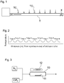
- Fig. 1 illustrates an embodiment of installing a temperature monitoring means to an exhaust tube.
- a plurality of thermocouples TC are installed on the exterior surface of an exhaust tube T at a predetermined interval, for example, at an approximately equal interval, and a crystal oscillator X is placed inside the tube at the most downstream location.
- the thermocouples TC may be replaced with surface thermometers or thermolabels.
- Chlorine trifluoride gas generates heat on reacting with silicon even at room temperature and chlorine trifluoride gas generates heat on reacting with carbon at elevated temperatures above about 100° to 200°C. On the other hand, it noticeably reacts with SiC to generate heat at temperatures from above 300° to 400°C.
- the monitoring starts with introducing chlorine trifluoride gas diluted with nitrogen to a concentration of 1 to 50 vol% into the exhaust tube T at a very small rate, e.g., about 10 cc/min, and the temperature near the gas inlet is measured.
- a very small rate e.g., about 10 cc/min
- the temperature near the gas inlet is measured.
- the chlorine trifluoride gas feed at a low flow rate, reaction between silicon and chlorosilane occurs to generate heat, and with the heat generated carbon starts reacting to generate heat. Thereby further occurring to generate heat, the temperature locally reaches a level allowing SiC to react. Because the reaction products, i.e., silicon fluoride and carbon fluoride, are low-boiling substances, they all turn into gas and clear out.
- a chlorine trifluoride concentration is dangerous in that the temperature of the generated heat excessively rises. At too low a concentration the temperature does not reach the level causing SiC to react. Therefore, it is necessary to select appropriate concentration and flow rate of chlorine trifluoride gas. For example, when chlorine trifluoride gas diluted with nitrogen to 10 vol% is fed at 10 cc/min, the site where a reaction takes place has an elevated temperature, and the site where a reaction has ended and the site where a reaction has not yet started show no temperature elevation. Thus, the location of the ongoing reaction is easily figured out by tracing the exterior surface temperatures of the exhaust tube T using the thermocouples TC.
- Fig. 2 displays an example of the temperature monitoring.
- the position of temperature elevation shifts from the upstream to downstream locations of the exhaust tube T with the passage of time from time 1, to time 2, ⁇ , to time N. This indicates that the site of the reaction with chlorine trifluoride gas shifts from upstream to downstream with time.
- the concentration of chlorine trifluoride gas fed to the exhaust tube T is preferably regulated so that the temperature measured on the outer surface of the tube T may not exceed 100°C.
- the flow rate of the chlorine trifluoride/nitrogen mixed gas is preferably regulated so that the temperature measured on the outer surface of the tube T may not exceed 100°C. The cleaning is determined to have completed when no temperature elevation as indicated in Fig. 2 is observed any more.
- the above illustrated technique is for determining the cleaning end point by using thermocouples TC installed to the exterior surface of the exhaust tube T.
- the cleaning end point can be determined by using the crystal oscillator X disposed inside the exhaust tube T as follows.
- the crystal oscillator X can be designed to have its frequency, e.g., 25 MHz increased or decreased with a rise in temperature and is therefore able to measure temperature changes sensitively.
- the temperature of the gas having reached to a sufficiently downstream site of the exhaust tube T is measured while feeding chlorine trifluoride gas to the exhaust tube T.
- the gas temperature gradually increases as the reaction site shifts downstream in the exhaust tube T, but the temperature of the gas reaching the crystal oscillator X decreases as a result of scale removal from the exhaust tube T. Removal of all the scale from the exhaust tube T is thus determined by this temperature decrease.
- the density and viscosity of the gas reaching the crystal oscillator X reduce. It is known that the frequency of a crystal oscillator is responsive to the product of the density and viscosity of gas. The frequency of the crystal oscillator increases with the consumption of chlorine trifluoride by the reactions. Therefore, the crystal oscillator X enables indirect determination of the gas composition as well as gas temperature measurement. Upon removal of the scale inside the exhaust tube T, the gas reaching the crystal oscillator X again increases in density and viscosity and thereby reduces in frequency, whereby scale removal is judged to be completed.
- ceasing the chlorine trifluoride gas feed on completion of cleaning inside the chamber and/or the exhaust tube be followed by thermally treating the inside of the chamber and/or the exhaust tube with at least one gas selected from the group consisting of nitrogen, argon, helium, and hydrogen.
- at least one gas selected from the group consisting of nitrogen, argon, helium, and hydrogen By the thermal treatment in such a gas atmosphere, fluorine vaporizes and is driven out of the system.
- the thermal treatment temperature is preferably set higher than the temperature at which the inside of the chamber and/or the inside of the exhaust tube are exposed to chlorine trifluoride gas irrespective of the kind of the gas.
- the thermal treatment temperature is preferably 500° to 1700°C, more preferably 900° to 1600°C, provided that it is higher than the temperature of exposure.
- the thermal treatment is preferably carried out at a temperature equal to or higher than the SiC fabrication temperature.
- the thermal treatment temperature is preferably 1500° to 2000°C, more preferably 1500° to 1700°C, provided that it is equal to or higher than the SiC fabrication temperature.
- the thermal treatment time is preferably 1 to 60 minutes, more preferably 1 to 10 minutes, provided that the thermal treatment temperature is in the above range.
- the thermal treatment atmosphere may be at least one of the above recited gases. Two or more of nitrogen, argon, and helium may be used in combination. Hydrogen is preferably used alone. In the case of using hydrogen, after stopping the feed of chlorine trifluoride gas to the system, it is preferred that hydrogen introduction be preceded by certainly removing chlorine trifluoride gas remaining in the system by, for example, purging. Purging the residual chloride trifluoride gas from the system may be achieved by, for example, evacuating the chamber to vacuum before hydrogen introduction as an atmosphere gas, or by feeding an inert gas, such as nitrogen, argon, or helium, through the system for a certain period of time (e.g., 10 minutes), followed by introducing hydrogen as an atmosphere gas. Feeding an inert gas may be performed with or without heat, e.g., at room temperature (25°C). The gas for thermal treatment may be fed to the chamber either in a continuous flow or batchwise.
- FIG. 3 is a schematic illustration of a testing device for confirming removal effect of residual fluorine atoms of the present invention.
- a numerical reference 10 indicates a quartz-made chamber.
- the chamber 10 has a volumetric capacity of 200 cm 3 .
- a high-purity carbon-made specimen 11 as a model susceptor.
- the specimen 11 has a SiC coating, which serves as model scale.
- a halogen lamp 12 is disposed outside the chamber 10 in a facing relation to the chamber 10.
- the nitrogen gas feed under heat was continued for 10 minutes to vaporize and remove fluorine atoms remaining on the specimen 11. Thereafter, feeding nitrogen gas was stopped and the halogen lamp 12 was turned off. After the chamber 10 cooled down, the specimen 11 was taken out from the chamber 10 and analyzed by XPS to determine the amount of fluorine atoms remaining on the surface of the specimen 11.
- the fluorine atoms remaining on the specimen 11 after the removal of SiC from the surface of the specimen 11 using chlorine trifluoride gas is reduced by the following thermal treatment in a nitrogen or hydrogen atmosphere as compared with the SiC removal without being followed by a thermal treatment. It is seen, in particular, that the thermal treatment in a hydrogen atmosphere achieves fluorine (atoms) removal to below the detection limit. The inventors have confirmed that such a trace amount of remaining fluorine atoms gives no adverse influences on ensuing SiC fabrication.
- the present invention enables effective removal of fluorine atoms remaining after cleaning a semiconductor fabrication chamber with chlorine trifluoride.
Landscapes
- Chemical & Material Sciences (AREA)
- Engineering & Computer Science (AREA)
- Mechanical Engineering (AREA)
- General Chemical & Material Sciences (AREA)
- Chemical Kinetics & Catalysis (AREA)
- Materials Engineering (AREA)
- Metallurgy (AREA)
- Organic Chemistry (AREA)
- Inorganic Chemistry (AREA)
- Chemical Vapour Deposition (AREA)
- Drying Of Semiconductors (AREA)
Applications Claiming Priority (2)
| Application Number | Priority Date | Filing Date | Title |
|---|---|---|---|
| JP2016169562 | 2016-08-31 | ||
| PCT/JP2017/030835 WO2018043446A1 (fr) | 2016-08-31 | 2017-08-29 | Procédé de nettoyage de chambre de production de semi-conducteur |
Publications (2)
| Publication Number | Publication Date |
|---|---|
| EP3509089A1 true EP3509089A1 (fr) | 2019-07-10 |
| EP3509089A4 EP3509089A4 (fr) | 2020-05-06 |
Family
ID=61301798
Family Applications (1)
| Application Number | Title | Priority Date | Filing Date |
|---|---|---|---|
| EP17846451.7A Withdrawn EP3509089A4 (fr) | 2016-08-31 | 2017-08-29 | Procédé de nettoyage de chambre de production de semi-conducteur |
Country Status (7)
| Country | Link |
|---|---|
| US (1) | US20210285100A1 (fr) |
| EP (1) | EP3509089A4 (fr) |
| JP (1) | JPWO2018043446A1 (fr) |
| KR (1) | KR20190042553A (fr) |
| CN (1) | CN109478510A (fr) |
| TW (1) | TW201812091A (fr) |
| WO (1) | WO2018043446A1 (fr) |
Cited By (1)
| Publication number | Priority date | Publication date | Assignee | Title |
|---|---|---|---|---|
| EP4064327A4 (fr) * | 2019-11-19 | 2023-01-18 | Showa Denko K.K. | Procédé de retrait de matériau d'adhérence et procédé de formation de film |
Families Citing this family (6)
| Publication number | Priority date | Publication date | Assignee | Title |
|---|---|---|---|---|
| JP7153582B2 (ja) * | 2019-02-01 | 2022-10-14 | 東京エレクトロン株式会社 | 成膜方法及び成膜装置 |
| JP7144608B2 (ja) * | 2019-05-08 | 2022-09-29 | 株式会社ニューフレアテクノロジー | 気相成長方法及び気相成長装置 |
| JP2021131312A (ja) * | 2020-02-20 | 2021-09-09 | 株式会社ミツトヨ | スケール |
| DE102020107518A1 (de) * | 2020-03-18 | 2021-09-23 | Aixtron Se | Verfahren zum Ermitteln des Endes eines Reinigungsprozesses der Prozesskammer eines MOCVD-Reaktors |
| CN117737695B (zh) * | 2023-12-20 | 2025-04-25 | 湖南德智新材料股份有限公司 | 一种清洁方法 |
| WO2025136086A1 (fr) * | 2023-12-22 | 2025-06-26 | Schunk Xycarb Technology B.V. | Procédé de nettoyage pour éliminer des excroissances parasites de carbures de silicium et une partie intérieure d'une chambre de traitement d'épitaxie et système de traitement d'épitaxie |
Family Cites Families (15)
| Publication number | Priority date | Publication date | Assignee | Title |
|---|---|---|---|---|
| JPH0663097B2 (ja) * | 1989-01-18 | 1994-08-17 | 岩谷産業株式会社 | 膜形成操作系におけるフツ化物系ガスによるクリーニング後の汚染除去方法 |
| JPH05243163A (ja) * | 1992-02-28 | 1993-09-21 | Kyocera Corp | 反応炉内部の残留ハロゲン除去方法 |
| JPH08306628A (ja) * | 1995-05-09 | 1996-11-22 | Toshiba Corp | 半導体形成装置およびそのクリーニング方法 |
| JP3056675B2 (ja) * | 1995-09-20 | 2000-06-26 | 株式会社荏原製作所 | 薄膜形成装置のClF3 によるクリーニングの終点検知法 |
| US6042654A (en) * | 1998-01-13 | 2000-03-28 | Applied Materials, Inc. | Method of cleaning CVD cold-wall chamber and exhaust lines |
| JP2001284264A (ja) * | 2000-03-31 | 2001-10-12 | Shin Etsu Handotai Co Ltd | 気相成長方法 |
| JP2003077839A (ja) * | 2001-08-30 | 2003-03-14 | Toshiba Corp | 半導体製造装置のパージ方法及び半導体装置の製造方法 |
| JP2003149058A (ja) * | 2001-11-14 | 2003-05-21 | Toshiba Corp | 温度センサ及びプラント温度計測装置 |
| JP2006237360A (ja) * | 2005-02-25 | 2006-09-07 | Iwate Toshiba Electronics Co Ltd | 半導体製造装置のガスクリーニングシステム |
| JP5550412B2 (ja) * | 2010-03-29 | 2014-07-16 | 岩谷産業株式会社 | 真空吸気配管のクリーニング方法 |
| JP5719720B2 (ja) * | 2011-08-19 | 2015-05-20 | 株式会社ニューフレアテクノロジー | 薄膜処理方法 |
| KR101427726B1 (ko) * | 2011-12-27 | 2014-08-07 | 가부시키가이샤 히다치 고쿠사이 덴키 | 기판 처리 장치 및 반도체 장치의 제조 방법 |
| US9416445B2 (en) * | 2012-02-08 | 2016-08-16 | Iwatani Corporation | Method for treating inner surface of chlorine trifluoride supply passage in apparatus using chlorine trifluoride |
| JP6242095B2 (ja) * | 2013-06-28 | 2017-12-06 | 株式会社日立国際電気 | クリーニング方法、半導体装置の製造方法、基板処理装置及びプログラム |
| JP6210039B2 (ja) * | 2014-09-24 | 2017-10-11 | セントラル硝子株式会社 | 付着物の除去方法及びドライエッチング方法 |
-
2017
- 2017-08-29 CN CN201780043539.7A patent/CN109478510A/zh active Pending
- 2017-08-29 JP JP2018537281A patent/JPWO2018043446A1/ja active Pending
- 2017-08-29 EP EP17846451.7A patent/EP3509089A4/fr not_active Withdrawn
- 2017-08-29 US US16/323,383 patent/US20210285100A1/en not_active Abandoned
- 2017-08-29 WO PCT/JP2017/030835 patent/WO2018043446A1/fr not_active Ceased
- 2017-08-29 KR KR1020197002778A patent/KR20190042553A/ko not_active Withdrawn
- 2017-08-30 TW TW106129473A patent/TW201812091A/zh unknown
Cited By (1)
| Publication number | Priority date | Publication date | Assignee | Title |
|---|---|---|---|---|
| EP4064327A4 (fr) * | 2019-11-19 | 2023-01-18 | Showa Denko K.K. | Procédé de retrait de matériau d'adhérence et procédé de formation de film |
Also Published As
| Publication number | Publication date |
|---|---|
| CN109478510A (zh) | 2019-03-15 |
| KR20190042553A (ko) | 2019-04-24 |
| EP3509089A4 (fr) | 2020-05-06 |
| TW201812091A (zh) | 2018-04-01 |
| JPWO2018043446A1 (ja) | 2019-07-25 |
| US20210285100A1 (en) | 2021-09-16 |
| WO2018043446A1 (fr) | 2018-03-08 |
Similar Documents
| Publication | Publication Date | Title |
|---|---|---|
| EP3509089A1 (fr) | Procédé de nettoyage de chambre de production de semi-conducteur | |
| US6844273B2 (en) | Precleaning method of precleaning a silicon nitride film forming system | |
| KR100767762B1 (ko) | 자가 세정을 위한 원격 플라즈마 소스를 구비한 cvd 반도체 공정장치 | |
| JP4459329B2 (ja) | 付着膜の除去方法及び除去装置 | |
| US20060016783A1 (en) | Process for titanium nitride removal | |
| CN1289860A (zh) | 化学汽相淀积装置及其净化方法和半导体制造装置 | |
| US6942892B1 (en) | Hot element CVD apparatus and a method for removing a deposited film | |
| US20050284575A1 (en) | Processing system and operating method of processing system | |
| JP7702965B2 (ja) | 水晶マイクロバランス濃度モニタ | |
| TW201905235A (zh) | 成膜裝置及其洗淨方法 | |
| JPH11345778A (ja) | 成膜装置のクリーニング方法及びそのクリーニング機構 | |
| JP2000323467A (ja) | 遠隔プラズマ放電室を有する半導体処理装置 | |
| JP5880974B2 (ja) | エピタキシャル成長装置の汚染検出方法及びエピタキシャルウェーハの製造方法 | |
| US20250198050A1 (en) | Reaction Furnace for Producing Polycrystalline Silicon Rod, Gas Supply Nozzle, Production Method of Polycrystalline Silicon Rod, and Polycrystalline Silicon Rod | |
| US20130239993A1 (en) | Film-forming apparatus and method for cleaning film-forming apparatus | |
| JP5936007B2 (ja) | 気相エピタキシャル成長装置の汚染評価方法及びエピタキシャルウェーハの製造方法 | |
| JP2559195B2 (ja) | シリコン基板上に塩化物がドープされた二酸化ケイ素膜を製造するための塩化オキサリルの使用 | |
| JP2005056925A (ja) | プラズマ処理装置および処理室内壁面安定化方法 | |
| US20260043131A1 (en) | Etching of silicon carbide films from reactor parts | |
| US20260018410A1 (en) | Method for controlling particle growth in a plasma chamber | |
| JP5370209B2 (ja) | シリコンエピタキシャルウェーハの製造方法 | |
| JPH10212582A (ja) | 薄膜形成装置の表面清浄に三フッ化塩素を用いる方法 | |
| JP6996952B2 (ja) | Iii族窒化物単結晶積層体の製造方法及びiii族窒化物単結晶積層体 | |
| JP2003144905A (ja) | ガスクリーニング方法 | |
| JP2008115473A (ja) | シリコン含有膜の製造装置及び製造法 |
Legal Events
| Date | Code | Title | Description |
|---|---|---|---|
| PUAI | Public reference made under article 153(3) epc to a published international application that has entered the european phase |
Free format text: ORIGINAL CODE: 0009012 |
|
| STAA | Information on the status of an ep patent application or granted ep patent |
Free format text: STATUS: REQUEST FOR EXAMINATION WAS MADE |
|
| 17P | Request for examination filed |
Effective date: 20190130 |
|
| AK | Designated contracting states |
Kind code of ref document: A1 Designated state(s): AL AT BE BG CH CY CZ DE DK EE ES FI FR GB GR HR HU IE IS IT LI LT LU LV MC MK MT NL NO PL PT RO RS SE SI SK SM TR |
|
| AX | Request for extension of the european patent |
Extension state: BA ME |
|
| DAV | Request for validation of the european patent (deleted) | ||
| DAX | Request for extension of the european patent (deleted) | ||
| A4 | Supplementary search report drawn up and despatched |
Effective date: 20200408 |
|
| RIC1 | Information provided on ipc code assigned before grant |
Ipc: H01L 21/67 20060101ALI20200402BHEP Ipc: H01L 21/31 20060101AFI20200402BHEP Ipc: H01L 21/02 20060101ALI20200402BHEP Ipc: H01L 21/3065 20060101ALI20200402BHEP Ipc: C23C 16/44 20060101ALI20200402BHEP Ipc: C23C 16/32 20060101ALI20200402BHEP |
|
| STAA | Information on the status of an ep patent application or granted ep patent |
Free format text: STATUS: THE APPLICATION IS DEEMED TO BE WITHDRAWN |
|
| 18D | Application deemed to be withdrawn |
Effective date: 20201110 |