EP3547008A1 - Appareil de guide d'onde optique et affichage - Google Patents
Appareil de guide d'onde optique et affichage Download PDFInfo
- Publication number
- EP3547008A1 EP3547008A1 EP19165080.3A EP19165080A EP3547008A1 EP 3547008 A1 EP3547008 A1 EP 3547008A1 EP 19165080 A EP19165080 A EP 19165080A EP 3547008 A1 EP3547008 A1 EP 3547008A1
- Authority
- EP
- European Patent Office
- Prior art keywords
- optical
- waveguide
- optical waveguide
- light
- transmitted
- Prior art date
- Legal status (The legal status is an assumption and is not a legal conclusion. Google has not performed a legal analysis and makes no representation as to the accuracy of the status listed.)
- Granted
Links
Images
Classifications
-
- G—PHYSICS
- G02—OPTICS
- G02B—OPTICAL ELEMENTS, SYSTEMS OR APPARATUS
- G02B27/00—Optical systems or apparatus not provided for by any of the groups G02B1/00 - G02B26/00, G02B30/00
- G02B27/01—Head-up displays
- G02B27/0101—Head-up displays characterised by optical features
-
- G—PHYSICS
- G02—OPTICS
- G02B—OPTICAL ELEMENTS, SYSTEMS OR APPARATUS
- G02B6/00—Light guides; Structural details of arrangements comprising light guides and other optical elements, e.g. couplings
- G02B6/10—Light guides; Structural details of arrangements comprising light guides and other optical elements, e.g. couplings of the optical waveguide type
- G02B6/12—Light guides; Structural details of arrangements comprising light guides and other optical elements, e.g. couplings of the optical waveguide type of the integrated circuit kind
- G02B6/122—Basic optical elements, e.g. light-guiding paths
-
- G—PHYSICS
- G02—OPTICS
- G02B—OPTICAL ELEMENTS, SYSTEMS OR APPARATUS
- G02B27/00—Optical systems or apparatus not provided for by any of the groups G02B1/00 - G02B26/00, G02B30/00
- G02B27/01—Head-up displays
- G02B27/017—Head mounted
- G02B27/0172—Head mounted characterised by optical features
-
- G—PHYSICS
- G02—OPTICS
- G02B—OPTICAL ELEMENTS, SYSTEMS OR APPARATUS
- G02B6/00—Light guides; Structural details of arrangements comprising light guides and other optical elements, e.g. couplings
-
- G—PHYSICS
- G02—OPTICS
- G02B—OPTICAL ELEMENTS, SYSTEMS OR APPARATUS
- G02B6/00—Light guides; Structural details of arrangements comprising light guides and other optical elements, e.g. couplings
- G02B6/0001—Light guides; Structural details of arrangements comprising light guides and other optical elements, e.g. couplings specially adapted for lighting devices or systems
- G02B6/0011—Light guides; Structural details of arrangements comprising light guides and other optical elements, e.g. couplings specially adapted for lighting devices or systems the light guides being planar or of plate-like form
- G02B6/0013—Means for improving the coupling-in of light from the light source into the light guide
- G02B6/0015—Means for improving the coupling-in of light from the light source into the light guide provided on the surface of the light guide or in the bulk of it
- G02B6/0016—Grooves, prisms, gratings, scattering particles or rough surfaces
-
- G—PHYSICS
- G02—OPTICS
- G02B—OPTICAL ELEMENTS, SYSTEMS OR APPARATUS
- G02B6/00—Light guides; Structural details of arrangements comprising light guides and other optical elements, e.g. couplings
- G02B6/0001—Light guides; Structural details of arrangements comprising light guides and other optical elements, e.g. couplings specially adapted for lighting devices or systems
- G02B6/0011—Light guides; Structural details of arrangements comprising light guides and other optical elements, e.g. couplings specially adapted for lighting devices or systems the light guides being planar or of plate-like form
- G02B6/0013—Means for improving the coupling-in of light from the light source into the light guide
- G02B6/0023—Means for improving the coupling-in of light from the light source into the light guide provided by one optical element, or plurality thereof, placed between the light guide and the light source, or around the light source
- G02B6/0031—Reflecting element, sheet or layer
-
- G—PHYSICS
- G02—OPTICS
- G02B—OPTICAL ELEMENTS, SYSTEMS OR APPARATUS
- G02B6/00—Light guides; Structural details of arrangements comprising light guides and other optical elements, e.g. couplings
- G02B6/0001—Light guides; Structural details of arrangements comprising light guides and other optical elements, e.g. couplings specially adapted for lighting devices or systems
- G02B6/0011—Light guides; Structural details of arrangements comprising light guides and other optical elements, e.g. couplings specially adapted for lighting devices or systems the light guides being planar or of plate-like form
- G02B6/0033—Means for improving the coupling-out of light from the light guide
- G02B6/005—Means for improving the coupling-out of light from the light guide provided by one optical element, or plurality thereof, placed on the light output side of the light guide
-
- G—PHYSICS
- G02—OPTICS
- G02B—OPTICAL ELEMENTS, SYSTEMS OR APPARATUS
- G02B6/00—Light guides; Structural details of arrangements comprising light guides and other optical elements, e.g. couplings
- G02B6/0001—Light guides; Structural details of arrangements comprising light guides and other optical elements, e.g. couplings specially adapted for lighting devices or systems
- G02B6/0011—Light guides; Structural details of arrangements comprising light guides and other optical elements, e.g. couplings specially adapted for lighting devices or systems the light guides being planar or of plate-like form
- G02B6/0033—Means for improving the coupling-out of light from the light guide
- G02B6/005—Means for improving the coupling-out of light from the light guide provided by one optical element, or plurality thereof, placed on the light output side of the light guide
- G02B6/0055—Reflecting element, sheet or layer
-
- G—PHYSICS
- G02—OPTICS
- G02B—OPTICAL ELEMENTS, SYSTEMS OR APPARATUS
- G02B6/00—Light guides; Structural details of arrangements comprising light guides and other optical elements, e.g. couplings
- G02B6/24—Coupling light guides
- G02B6/26—Optical coupling means
- G02B6/34—Optical coupling means utilising prism or grating
-
- G—PHYSICS
- G03—PHOTOGRAPHY; CINEMATOGRAPHY; ANALOGOUS TECHNIQUES USING WAVES OTHER THAN OPTICAL WAVES; ELECTROGRAPHY; HOLOGRAPHY
- G03B—APPARATUS OR ARRANGEMENTS FOR TAKING PHOTOGRAPHS OR FOR PROJECTING OR VIEWING THEM; APPARATUS OR ARRANGEMENTS EMPLOYING ANALOGOUS TECHNIQUES USING WAVES OTHER THAN OPTICAL WAVES; ACCESSORIES THEREFOR
- G03B21/00—Projectors or projection-type viewers; Accessories therefor
- G03B21/14—Details
- G03B21/147—Optical correction of image distortions, e.g. keystone
-
- G—PHYSICS
- G03—PHOTOGRAPHY; CINEMATOGRAPHY; ANALOGOUS TECHNIQUES USING WAVES OTHER THAN OPTICAL WAVES; ELECTROGRAPHY; HOLOGRAPHY
- G03B—APPARATUS OR ARRANGEMENTS FOR TAKING PHOTOGRAPHS OR FOR PROJECTING OR VIEWING THEM; APPARATUS OR ARRANGEMENTS EMPLOYING ANALOGOUS TECHNIQUES USING WAVES OTHER THAN OPTICAL WAVES; ACCESSORIES THEREFOR
- G03B21/00—Projectors or projection-type viewers; Accessories therefor
- G03B21/14—Details
- G03B21/20—Lamp housings
- G03B21/2066—Reflectors in illumination beam
-
- G—PHYSICS
- G02—OPTICS
- G02B—OPTICAL ELEMENTS, SYSTEMS OR APPARATUS
- G02B27/00—Optical systems or apparatus not provided for by any of the groups G02B1/00 - G02B26/00, G02B30/00
- G02B27/01—Head-up displays
- G02B27/0101—Head-up displays characterised by optical features
- G02B2027/0112—Head-up displays characterised by optical features comprising device for genereting colour display
-
- G—PHYSICS
- G02—OPTICS
- G02B—OPTICAL ELEMENTS, SYSTEMS OR APPARATUS
- G02B27/00—Optical systems or apparatus not provided for by any of the groups G02B1/00 - G02B26/00, G02B30/00
- G02B27/01—Head-up displays
- G02B27/0101—Head-up displays characterised by optical features
- G02B2027/0118—Head-up displays characterised by optical features comprising devices for improving the contrast of the display / brillance control visibility
Definitions
- the disclosure relates to an optical apparatus, and in particular, to an optical waveguide apparatus and a display including the optical waveguide apparatus.
- a diffractive waveguide involves a method based on the principle of optical diffraction in which a diffraction phenomenon occurs after a light passes through slit-like microstructures, such that a direction of the light is changed.
- optical efficiency is the biggest issue. Due to the diffraction element, much energy is lost because zero-order light is not re-used.
- properties including the cycle, the material, and the shape of the optical microstructures all influence the progression direction, the progression angle, and efficiency of the light. Therefore, how to design high-efficiency optical microstructures and maintain manufacturing feasibility is one of the issues to overcome in the field of diffractive waveguides.
- the loss in optical energy is reduced by changing the optical microstructures.
- it is difficult to effectively control the quality of the optical microstructures in production. Therefore, the issue of low light transmission efficiency is still present in the diffractive waveguides currently available.
- the embodiments of the invention provide an optical waveguide apparatus that effectively enhances light beam transmission efficiency of the optical waveguide apparatus and reduces optical energy loss caused in a light beam output by a projection apparatus to the optical waveguide apparatus to enhance a brightness of an image displayed by a display including the optical waveguide apparatus and meanwhile effectively maintain a resolution of the image. Moreover, a color temperature of the light beam output by the optical waveguide apparatus is substantially consistent with a color temperature of a light beam output by the projection apparatus.
- an embodiment of the invention provides an optical waveguide apparatus including an optical waveguide element and an optical recycling element.
- the optical waveguide element includes a first surface and a second surface opposite to the first surface.
- the first surface or the second surface includes an optical structure.
- An incident light enters the optical waveguide element via the first surface and is transmitted to the second surface.
- the optical recycling element is disposed on the second surface of the optical waveguide element. The incident light is transmitted to the optical recycling element via the second surface.
- the optical recycling element changes a transmission direction of the incident light to generate a recycled light.
- the recycled light enters the optical waveguide element via the second surface and is transmitted to the first surface.
- the incident light and the recycled light are transmitted in the optical waveguide element.
- the optical structure may be disposed on the first surface of the optical waveguide element.
- the incident light enters the optical waveguide element by refractive diffraction via the first surface.
- the recycled light is transmitted to the first surface via the second surface and undergoes reflective diffraction at the optical structure to be transmitted in the optical waveguide element.
- the optical structure may be disposed on the second surface of the optical waveguide element
- the incident light is transmitted to the second surface via the first surface and undergoes reflective diffraction at the optical structure to be transmitted in the optical waveguide element.
- the recycled light enters the optical waveguide element by refractive diffraction via the second surface.
- the optical recycling element may be selected from one of a reflection mirror, a band pass filter, a dichroic mirror, a diffraction element, and a planar optical element.
- the optical recycling element comprises an optical film layer.
- the optical film layer may be disposed on a surface of the optical structure.
- the optical waveguide element may comprise one single waveguide plate.
- the first surface and the second surface are two opposite surfaces of the one single waveguide plate.
- the optical waveguide element comprises a first waveguide plate and a second waveguide plate.
- the first waveguide plate and the second waveguide plate each comprise the optical structure.
- the first waveguide plate and the second waveguide plate are arranged in parallel along a light transmission direction.
- the first surface is a surface where the first waveguide plate receives the incident light
- the second surface is a surface where the second waveguide plate faces the optical recycling element
- the optical waveguide element may comprises a first waveguide plate, a second waveguide plate, and a third waveguide plate.
- the first waveguide plate, the second waveguide plate, and the third waveguide plate each comprises the optical structure.
- the first waveguide plate, the second waveguide plate, and the third waveguide plate are arranged in parallel along a light transmission direction, the first surface is a surface where the first waveguide plate receives the incident light, and the second surface is a surface where the third waveguide plate faces the optical recycling element.
- the incident light comprises a first color light, a second color light, and a third color light.
- the first color light is transmitted in the first waveguide plate
- the second color light is transmitted in the second waveguide plate
- the third color light is transmitted in the third waveguide plate.
- the optical recycling element may be further disposed between the first waveguide plate and the second waveguide plate and between the second waveguide plate and the third waveguide plate.
- the optical waveguide apparatus may further comprise a protective element disposed on a side of the second surface of the optical waveguide element.
- the optical recycling element is disposed between the optical waveguide element and the protective element.
- the first surface may comprise the optical structure.
- the incident light may enter the optical waveguide element via the first surface and may be transmitted to the second surface.
- the optical recycling element may be integrally formed on the second surface of the optical waveguide element, wherein the optical recycling element is a diffraction element.
- the optical waveguide element may comprise another optical structure, and the incident light and the recycled light are transmitted to a projection target via the other optical structure.
- an embodiment of the invention provides a display for projecting an image light beam to a projection target, and the display includes a projection apparatus and an optical waveguide apparatus.
- the projection apparatus projects an incident light, and the incident light is the image light beam.
- the optical waveguide apparatus includes an optical waveguide element and an optical recycling element.
- the optical waveguide element includes a first surface and a second surface opposite to the first surface. The first surface or the second surface includes an optical structure. An incident light enters the optical waveguide element via the first surface and is transmitted to the second surface.
- the optical recycling element is disposed on the second surface of the optical waveguide element. The incident light is transmitted to the optical recycling element via the second surface.
- the optical recycling element changes a transmission direction of the incident light to generate a recycled light.
- the recycled light enters the optical waveguide element via the second surface and is transmitted to the first surface.
- the incident light and the recycled light are transmitted in the optical waveguide element and are transmitted to the projection target.
- the optical waveguide apparatus of the embodiments of the invention includes the optical recycling element and effectively enhances light beam transmission efficiency of the optical waveguide apparatus and reduces optical energy loss caused in a light beam output by the projection apparatus to the optical waveguide apparatus to enhance a brightness of an image displayed by the display including the optical waveguide apparatus and meanwhile effectively maintain a resolution of the image.
- a color temperature of the light beam output by the optical waveguide apparatus is substantially consistent with a color temperature of a light beam output by the projection apparatus.
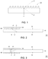
- FIG. 1 is a schematic diagram illustrating an optical structure according to an embodiment of the invention.
- an incident light L1 enters an optical structure 130
- diffraction effect of light occurs. Therefore, when the incident light L1 passes through a light-transmissive microstructure region, a reflective diffracted light L2 and a refractive diffracted light L3 are generated.
- the diffracted light L2 and the diffracted light L3 are first-order diffracted lights.
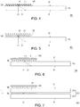
- FIG. 2 is a schematic diagram illustrating an optical waveguide apparatus according to an embodiment of the invention.
- an optical waveguide apparatus 100 of the embodiment includes an optical waveguide element 110 and an optical recycling element 120.
- the optical waveguide element 110 includes a first surface S1 and a second surface S2.
- the second surface S2 is opposite to the first surface S1 and includes the optical structure 130.
- the optical recycling element 120 is disposed on a side of the second surface S2 of the optical waveguide element 110.
- the incident light L1 enters the optical waveguide element 110 via the first surface S1.
- the incident light L1 is transmitted to the optical structure 130 of the second surface S2 to generate the reflective diffracted light L2.
- the incident light L1 is transmitted to the optical recycling element 120 via the optical structure 130 of the second surface S2.
- the optical recycling element 120 changes a transmission direction of the incident light L1 to generate a recycled light L4.
- the recycled light L4 is, for example, a zero-order diffracted light that is generated after the incident light L1 passes through the optical structure 130 and is reflected by the optical recycling element 120 and then enters the optical waveguide element 110 again.
- the recycled light L4 may also be a first-order or high-order diffracted light.
- the recycled light L4 enters the optical waveguide element 110 via the optical structure 130 of the second surface S2 and is transmitted to the first surface S1.
- a refractive diffracted light L5 is generated.
- the diffracted light L2 is a portion of the incident light L1 and is transmitted in the optical waveguide element 110.
- the diffracted light L5 is a portion of the recycled light L4 and is transmitted in the optical waveguide element 110.
- the incident light L1 is reflected by the optical recycling element 120 due to the optical structure 130 and enters the optical waveguide element 110 again via the optical structure 130 to be transmitted in the optical waveguide element 110. Therefore, light utilization efficiency of the optical waveguide element 110 can be enhanced.
- FIG. 3 is a schematic diagram illustrating an optical waveguide apparatus according to another embodiment of the invention.
- an optical waveguide apparatus 200 of the embodiment is similar to the optical waveguide apparatus 100 of FIG. 2 , and a difference between the two lies in, for example, including the optical structure 130 on the first surface S1.
- the incident light L1 enters the optical waveguide element 110 via the first surface S1, and a refractive diffracted light L3 is generated at the optical structure 130.
- the incident light L1 is transmitted to the optical recycling element 120 via the second surface S2.
- the optical recycling element 120 changes a transmission direction of the incident light L1 to generate a recycled light L4.
- the recycled light L4 is, for example, a zero-order diffracted light that is generated after the incident light L1 passes through the optical structure 130 and is reflected by the optical recycling element 120 and then enters the optical waveguide element 110 again.
- the recycled light L4 may also be a first-order or high-order diffracted light.
- the recycled light L4 enters the optical waveguide element 110 via the second surface S2.
- the recycled light L4 is transmitted to the first surface S1 to generate a reflective diffracted light L6 at the optical structure 130.
- the reflective diffracted light L6 is generated.
- the diffracted light L3 is a portion of the incident light L1 and is transmitted in the optical waveguide element 110.
- the diffracted light L6 is a portion of the recycled light L4 and is transmitted in the optical waveguide element 110.
- the incident light L1 is reflected by the optical recycling element 120 due to the optical structure 130 and enters the optical waveguide element 110 again via the optical structure 130 to be transmitted in the optical waveguide element 110. Therefore, light utilization efficiency of the optical waveguide element 110 can be enhanced.
- the optical recycling element 120 is, for example, an optical element having a reflection function, such as a reflection mirror, a band pass filter, and a dichroic mirror.
- the optical recycling element 120 may also be an optical film layer, a diffraction element, or a planar optical element.
- FIG. 4 is a schematic diagram illustrating an optical waveguide apparatus according to another embodiment of the invention.
- an optical waveguide apparatus 300 of the embodiment is similar to the optical waveguide apparatus 100 of FIG. 2 , and a difference between the two lies in, for example, that an optical recycling element 140 of the embodiment is, for example, an optical film layer.
- the optical recycling element 140 is formed by coating a reflective material on the surface of the optical structure 130 and is configured to reflect the diffracted light transmitted from the optical waveguide element 110, such that the diffracted light enters the optical waveguide element 110 again. Thereby, light utilization efficiency of the optical waveguide element 110 can be enhanced.
- FIG. 5 is a schematic diagram illustrating an optical waveguide apparatus according to another embodiment of the invention.
- an optical waveguide apparatus 400 of the embodiment is similar to the optical waveguide apparatus 100 of FIG. 2 , and a difference between the two lies in, for example, that an optical recycling element 150 of the embodiment is, for example, a diffraction element having a reflection function.
- the diffraction element may include another optical structure different from the optical structure 130 or includes a grating structure.
- the optical recycling element 150 is disposed on a side of the second surface S2 of the optical waveguide element 110 to reflect the diffracted light transmitted from the optical structure 130, such that the diffracted light enters the optical waveguide element 110 again. Thereby, light utilization efficiency of the optical waveguide element 110 can be enhanced.
- FIG. 6 is a schematic diagram illustrating an optical waveguide apparatus according to another embodiment of the invention.
- an optical waveguide apparatus 500 of the embodiment is similar to the optical waveguide apparatus 100 of FIG. 2 , and a difference between the two lies in, for example, that an optical recycling element 160 of the embodiment is, for example, a planar optical element.
- the planar optical element is, for example, a liquid crystal lens, a Fresnel lens, or is an optical element including a metasurface.
- the optical recycling element 160 is disposed on a side of the second surface S2 of the optical waveguide element 110 to reflect the diffracted light, such that the diffracted light enters the optical waveguide element 110 again. Thereby, light utilization efficiency of the optical waveguide element 110 can be enhanced.
- the optical waveguide element 110 includes one single waveguide plate, but the invention is not limited hereto.
- the optical waveguide element may also include a plurality of waveguide plates.
- FIG. 7 is a schematic diagram illustrating an optical waveguide apparatus according to another embodiment of the invention.
- an optical waveguide apparatus 600 of the embodiment is similar to the optical waveguide apparatus 100 of FIG. 2 , and a difference between the two lies in, for example, that an optical waveguide element 210 of the embodiment includes a first waveguide plate 212 and a second waveguide plate 214.
- the first waveguide plate 212 and the second waveguide plate 214 are arranged in parallel along a transmission direction Z of the incident light L1.
- the first waveguide plate 212 and the second waveguide plate 214 each include the optical structure 130.
- the first surface S1 is the surface where the first waveguide plate 212 receives the incident light L1
- the second surface S2 is the surface where the second waveguide plate 214 faces the optical recycling element 120.
- the optical recycling element 120 is disposed on a side of the second surface S2 of the second waveguide plate 214 to reflect the diffracted light, such that the diffracted light enters the first waveguide plate 212 and the second waveguide plate 214 again. Thereby, light utilization efficiency of the optical waveguide element 210 can be enhanced.
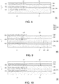
- FIG. 8 is a schematic diagram illustrating an optical waveguide apparatus according to another embodiment of the invention.
- an optical waveguide apparatus 700 of the embodiment is similar to the optical waveguide apparatus 100 of FIG. 2 , and a difference between the two lies in, for example, that an optical waveguide element 310 of the embodiment includes a first waveguide plate 312, a second waveguide plate 314, and a third waveguide plate 316, and an optical recycling element 320 is an optical film layer disposed on the second surface S2 of the optical waveguide element 310.
- the first waveguide plate 312, the second waveguide plate 314, and the third waveguide plate 316 are arranged in parallel along the transmission direction Z of the incident light L1.
- the first waveguide plate 312, the second waveguide plate 314, and the third waveguide plate 316 each include the optical structure 130.
- the first surface S1 is the surface where the first waveguide plate 312 receives the incident light L1
- the second surface S2 is the surface where the third waveguide plate 316 faces the optical recycling element 320.
- the incident light L1 includes a first color light, a second color light, and a third color light.
- the first color light is transmitted in the first waveguide plate 312, the second color light is transmitted in the second waveguide plate 314, and the third color light is transmitted in the third waveguide plate 316.
- the first waveguide plate 312, the second waveguide plate 314, and the third waveguide plate 316 are dichroic elements or polarizers (not illustrated) but are not limited hereto.
- the first color light, the second color light, and the third color light may be controlled to be transmitted respectively in the first waveguide plate 312, the second waveguide plate 314, and the third waveguide plate 316.
- the first waveguide plate 312, the second waveguide plate 314, and the third waveguide plate 316 are, for example, respectively a blue light waveguide plate, a green light waveguide plate, and a red light waveguide plate
- the first color light, the second color light, and the third color light are, for example, respectively a blue light, a green light, and a red light.
- the incident light L1 enters the optical waveguide element 310 via the first surface S1 and sequentially passes through the blue light waveguide plate, the green light waveguide plate, and the red light waveguide plate. Therefore, the blue light of the incident light L1 has the highest output efficiency, and the red light has the lowest output efficiency. At this time, there is a case of a slightly high color temperature.
- the recycled light L4 enters the optical waveguide element 310 via the second surface S2, it sequentially passes through the red light waveguide plate, the green light waveguide plate, and the blue light waveguide plate. Therefore, the blue light of the recycled light L4 has the lowest output efficiency, and the red light has the highest output efficiency.
- the recycled light L4 is reflected back to the optical waveguide element 310 by the optical recycling element 320 to compensate for the lower output efficiency of the red light of the incident light L1, and thereby the color temperature of the light output by the optical waveguide element 310 is more uniform.
- FIG. 9 is a schematic diagram illustrating an optical waveguide apparatus according to another embodiment of the invention.
- an optical waveguide apparatus 800 of the embodiment is similar to the optical waveguide apparatus 700 of FIG. 8 , and a difference between the two lies in, for example, that the optical recycling element 320 includes a plurality of optical film layers 322, 324, 326.
- the optical film layers 322, 324, 326 are, for example, the optical recycling element 320.
- the optical film layer 322 is disposed between the first waveguide plate 312 and the second waveguide plate 314.
- the optical film layer 324 is disposed between the second waveguide plate 314 and the third waveguide plate 316.
- the optical film layer 326 is disposed on the second surface S2 of the optical waveguide element 310.
- FIG. 10 is a schematic diagram illustrating an optical waveguide apparatus according to another embodiment of the invention.
- an optical waveguide apparatus 900 of the embodiment is similar to the optical waveguide apparatus 700 of FIG. 8 , and a difference between the two lies in, for example, that the optical waveguide apparatus 900 further includes a protective element 970, and an optical recycling element 920 is disposed between the optical waveguide element 310 and the protective element 970.
- the protective element 970 is disposed on a side of the second surface S2 of the optical waveguide element 310.
- the protective element 970 is, for example, a cover glass.
- the optical recycling element 920 may also be disposed between the optical waveguide element 310 and the cover glass.
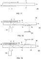
- FIG. 11 is a schematic diagram illustrating an optical waveguide apparatus according to still another embodiment of the invention.
- an optical waveguide apparatus 1000 of the embodiment includes an optical waveguide element 110 and an optical recycling element 120.
- the optical waveguide element 110 includes a first surface S1 and a second surface S2.
- the second surface S2 is opposite to the first surface S1, and the first surface S1 includes an optical structure 130.
- the optical recycling element 120 is disposed on the second surface S2 of the optical waveguide element 110.
- the optical recycling element 120 is integrally formed on the second surface S2 of the optical waveguide element 110.
- An incident light L1 is reflected due to the optical recycling element 120 and enters the optical waveguide element 110 again to be transmitted in the optical waveguide element 110. Therefore, light utilization efficiency of the optical waveguide element 110 can be enhanced.
- FIG. 12 is a schematic diagram illustrating a display according to another embodiment of the invention.
- a display 1001 of the embodiment includes a projection apparatus 1010 and an optical waveguide apparatus 100.
- the projection apparatus 1010 includes a light valve element to project an incident light L1.
- the incident light L1 is an image light beam.
- the light valve element is, for example, a reflective or transmissive spatial light modulator.
- the reflective spatial light modulator includes, for example, a reflective liquid crystal on silicon (LCOS) or a digital micro-mirror device (DMD).
- the transmissive spatial light modulator includes, for example, a transparent liquid crystal panel.
- the optical waveguide apparatus 100 includes an optical waveguide element 110 and an optical recycling element 120.
- the optical waveguide element 110 includes a first surface S1 and a second surface S2.
- the second surface S2 is opposite to the first surface S1 and includes an optical structure 130.
- the optical recycling element 120 is disposed on a side of the second surface S2 of the optical waveguide element 110.
- the incident light L1 enters the optical waveguide element 110 via the first surface S1.
- the incident light L1 is transmitted to the optical structure 130 of the second surface S2 to generate a reflective diffracted light L2.
- the incident light L1 is transmitted to the optical recycling element 120 via the optical structure 130 of the second surface S2.
- the optical recycling element 120 changes a transmission direction of the incident light L1 to generate a recycled light L4.
- the recycled light L4 is, for example, a zero-order diffracted light that is generated after the incident light L1 passes through the optical structure 130 and is reflected by the optical recycling element 120 and then enters the optical waveguide element 110 again.
- the recycled light L4 may also be a first-order or high-order diffracted light.
- the recycled light L4 enters the optical waveguide element 110 via the optical structure 130 of the second surface S2 and is transmitted to the first surface S1.
- a refractive diffracted light L5 is generated.
- the diffracted light L2 is a portion of the incident light L1 and is transmitted in the optical waveguide element 110.
- the diffracted light L5 is a portion of the recycled light L4 and is transmitted in the optical waveguide element 110.
- the incident light L1 is reflected by the optical recycling element 120 due to the optical structure 130 and enters the optical waveguide element 110 again via the optical structure 130 to be transmitted in the optical waveguide element 110. Therefore, light utilization efficiency of the optical waveguide element 110 can be enhanced.
- the diffracted light L2 and the diffracted light L5 are transmitted in total reflection in the optical waveguide element 110 to a position of the first surface S1 at which another optical structure 230 is disposed.
- the diffracted light L2 and the diffracted light L5 pass through the optical waveguide element 110 via the optical structure 230 and are transmitted to a projection target 1020.
- the projection target 1020 is, for example, a human eye or a light beam receiver (e.g., a camera or an optical sensor) but is not limited hereto.
- the optical recycling element 120 and the second surface S2 are disposed in parallel to each other so that a brightness of an image is enhanced without lowering a resolution of the image.
- the optical recycling element 120 and the second surface S2 are not disposed in parallel to each other, if the optical recycling element 120 is rotated by an angle (e.g., 2°) along a first-axis direction (X) or the optical recycling element 120 is rotated by an angle (e.g., 2°) along a second-axis direction (Y) such that an included angle is present between the optical recycling element 120 and the second surface S2, the image is offset and the resolution is thus lowered.
- FIG. 13 is a schematic diagram illustrating a display according to another embodiment of the invention.
- a display 1002 of the embodiment is similar to the display 1001 of FIG. 12 , and a difference between the two lies in, for example, that the other optical structure 230 of the embodiment is disposed on the second surface S2 of the optical waveguide element 110.
- the diffracted light L2 and the diffracted light L5 are transmitted in total reflection in the optical waveguide element 110 to the position of the optical structure 230 of the second surface S2.
- the diffracted light L2 and the diffracted light L5 pass through the optical waveguide element 110 via the optical structure 230 and are transmitted to a projection target 1020.
- the projection target 1020 is, for example, a human eye or a light beam receiver (e.g., a CCD (charge-coupled device), a CMOS (complementary metal-oxide semiconductor), etc.) but is not limited hereto.
- a light beam receiver e.g., a CCD (charge-coupled device), a CMOS (complementary metal-oxide semiconductor), etc.
- the diffracted light L2 and the diffracted light L5 are transmitted out of the optical waveguide element 110 and are transmitted to the projection target 1020.
- the invention does not limit that the diffracted light beam has to leave the optical waveguide element 110 via the first surface S1 if the optical structure 230 is disposed on the first surface S1. It is also possible that the diffracted light beam may leave the optical waveguide element 110 via the second surface S2, which shall depend on the manufacturer's design of the light travel paths.
- the optical waveguide apparatus includes the optical recycling element that reflects the incident light and generates the recycled light to enhance optical efficiency of the optical waveguide apparatus.
- the optical waveguide element may include one or a plurality of waveguide plates.
- the optical recycling element may also be disposed between each two of the plurality of waveguide plates.
- the optical waveguide element may include waveguide plates of different colors that function with the optical recycling element to compensate for the color temperature, such that the color temperature of the light output by the optical waveguide apparatus is more consistent with that output by the optical machine.
- the term "the invention”, “the present invention” or the like does not necessarily limit the claim scope to a specific embodiment, and the reference to particularly preferred exemplary embodiments of the invention does not imply a limitation on the invention, and no such limitation is to be inferred.
- the invention is limited only by the scope of the appended claims.
- the abstract of the disclosure is provided to comply with the rules requiring an abstract, which will allow a searcher to quickly ascertain the subject matter of the technical disclosure of any patent issued from this disclosure. It is submitted with the understanding that it will not be used to interpret or limit the scope or meaning of the claims. Any advantages and benefits described may not apply to all embodiments of the invention.
Landscapes
- Physics & Mathematics (AREA)
- General Physics & Mathematics (AREA)
- Optics & Photonics (AREA)
- Engineering & Computer Science (AREA)
- Microelectronics & Electronic Packaging (AREA)
- Optical Couplings Of Light Guides (AREA)
- Projection Apparatus (AREA)
- Optical Integrated Circuits (AREA)
- Diffracting Gratings Or Hologram Optical Elements (AREA)
Applications Claiming Priority (1)
| Application Number | Priority Date | Filing Date | Title |
|---|---|---|---|
| CN201810297008.7A CN110320588A (zh) | 2018-03-30 | 2018-03-30 | 光波导装置及显示器 |
Publications (2)
| Publication Number | Publication Date |
|---|---|
| EP3547008A1 true EP3547008A1 (fr) | 2019-10-02 |
| EP3547008B1 EP3547008B1 (fr) | 2024-11-06 |
Family
ID=65991556
Family Applications (1)
| Application Number | Title | Priority Date | Filing Date |
|---|---|---|---|
| EP19165080.3A Active EP3547008B1 (fr) | 2018-03-30 | 2019-03-26 | Appareil de guide d'onde optique et affichage |
Country Status (4)
| Country | Link |
|---|---|
| US (1) | US10871613B2 (fr) |
| EP (1) | EP3547008B1 (fr) |
| JP (1) | JP7378215B2 (fr) |
| CN (1) | CN110320588A (fr) |
Cited By (1)
| Publication number | Priority date | Publication date | Assignee | Title |
|---|---|---|---|---|
| US12242059B2 (en) | 2019-04-25 | 2025-03-04 | Snap Inc. | Display for augmented reality |
Families Citing this family (5)
| Publication number | Priority date | Publication date | Assignee | Title |
|---|---|---|---|---|
| US20240103270A1 (en) * | 2019-11-06 | 2024-03-28 | Google Llc | Optical combiners with improved efficiency and uniformity |
| CN114641713A (zh) * | 2019-11-08 | 2022-06-17 | 奇跃公司 | 具有包括多种材料的光重定向结构的超表面以及制造方法 |
| WO2021254603A1 (fr) * | 2020-06-17 | 2021-12-23 | Huawei Technologies Co., Ltd. | Dispositif optique pour atténuer une bande sombre dans un dispositif de réalité augmentée |
| WO2022192142A1 (fr) * | 2021-03-09 | 2022-09-15 | Applied Materials, Inc. | Empilement de métalentilles sur des combinateurs de guides d'ondes pour lunettes ar/vr |
| FI132003B1 (en) * | 2023-08-24 | 2026-04-02 | Dispelix Oy | Screen structure |
Citations (4)
| Publication number | Priority date | Publication date | Assignee | Title |
|---|---|---|---|---|
| EP2196729A1 (fr) * | 2008-12-12 | 2010-06-16 | BAE Systems PLC | Améliorations de guides d'ondes ou relatives à ceux-ci |
| US20160077338A1 (en) * | 2014-09-16 | 2016-03-17 | Steven John Robbins | Compact Projection Light Engine For A Diffractive Waveguide Display |
| US20170255016A1 (en) * | 2016-03-01 | 2017-09-07 | Magic Leap, Inc. | Reflective switching device for inputting different wavelengths of light into waveguides |
| US20180082644A1 (en) * | 2016-09-22 | 2018-03-22 | Microsoft Technology Licensing, Llc | Display engines for use with optical waveguides |
Family Cites Families (28)
| Publication number | Priority date | Publication date | Assignee | Title |
|---|---|---|---|---|
| JPH11174270A (ja) * | 1997-12-09 | 1999-07-02 | Minolta Co Ltd | 光導波路入出力装置 |
| JPH11281833A (ja) * | 1998-03-31 | 1999-10-15 | Minolta Co Ltd | グレーティングカプラ |
| JP4197813B2 (ja) * | 1999-11-02 | 2008-12-17 | 日東電工株式会社 | 液晶表示装置 |
| JP2002124115A (ja) * | 2000-08-08 | 2002-04-26 | Yuka Denshi Co Ltd | 面光源装置及びこれを用いた液晶ディスプレイ装置 |
| EP1639394A2 (fr) * | 2003-06-10 | 2006-03-29 | Elop Electro-Optics Industries Ltd. | Procede et systeme servant a afficher une image informative sur une image d'arriere-plan |
| JP2006285222A (ja) * | 2005-03-09 | 2006-10-19 | Konica Minolta Holdings Inc | 回折光学素子及び光通信モジュール |
| TWI265277B (en) * | 2005-05-11 | 2006-11-01 | Ind Tech Res Inst | Integrated fiber optic gyro sensing device |
| TW200641416A (en) * | 2005-05-31 | 2006-12-01 | Bright View Electronics Co Ltd | A lighting device providing longitudinal illumination |
| SE529254C2 (sv) * | 2005-06-17 | 2007-06-12 | Aamic Ab | Optiskt testsystem |
| IL171820A (en) * | 2005-11-08 | 2014-04-30 | Lumus Ltd | A polarizing optical component for light coupling within a conductive substrate |
| TWI367567B (en) * | 2008-11-26 | 2012-07-01 | Univ Nat Central | Guided mode resonance solar cell |
| ES2721600T5 (es) * | 2008-12-12 | 2022-04-11 | Bae Systems Plc | Mejoras en o relacionadas con guías de onda |
| JP5545076B2 (ja) * | 2009-07-22 | 2014-07-09 | ソニー株式会社 | 画像表示装置及び光学装置 |
| CN104089701B (zh) * | 2010-05-07 | 2016-11-09 | 台湾超微光学股份有限公司 | 光学系统 |
| TWI452402B (zh) * | 2010-12-08 | 2014-09-11 | Au Optronics Corp | 顯示元件 |
| US8189263B1 (en) | 2011-04-01 | 2012-05-29 | Google Inc. | Image waveguide with mirror arrays |
| JP5879886B2 (ja) * | 2011-10-03 | 2016-03-08 | セイコーエプソン株式会社 | 虚像表示装置及びその製造方法 |
| US9995876B2 (en) * | 2012-07-30 | 2018-06-12 | Hewlett Packard Enterprise Development Lp | Configurable compact photonic platforms |
| JP6287095B2 (ja) * | 2013-11-19 | 2018-03-07 | セイコーエプソン株式会社 | 光学デバイス及び電子機器 |
| US9341883B2 (en) * | 2014-02-07 | 2016-05-17 | Himax Display, Inc. | Display module and light guide device |
| JP6287487B2 (ja) * | 2014-03-31 | 2018-03-07 | セイコーエプソン株式会社 | 光学デバイス、画像投影装置及び電子機器 |
| US20170030788A1 (en) | 2014-04-10 | 2017-02-02 | Motion Engine Inc. | Mems pressure sensor |
| WO2016111707A1 (fr) * | 2015-01-10 | 2016-07-14 | Leia Inc. | Guide de lumière couplé à un réseau |
| IL237337B (en) * | 2015-02-19 | 2020-03-31 | Amitai Yaakov | A compact head-up display system with a uniform image |
| JP2016188901A (ja) * | 2015-03-30 | 2016-11-04 | セイコーエプソン株式会社 | 表示装置 |
| IL256276B (en) * | 2015-06-15 | 2022-09-01 | Magic Leap Inc | Display system with optical components for coupling multiple light streams |
| US10473933B2 (en) * | 2016-02-19 | 2019-11-12 | Microsoft Technology Licensing, Llc | Waveguide pupil relay |
| KR102646158B1 (ko) * | 2016-12-13 | 2024-03-11 | 엘지디스플레이 주식회사 | 광학식 이미지 인식 센서 내장형 평판 표시장치 |
-
2018
- 2018-03-30 CN CN201810297008.7A patent/CN110320588A/zh active Pending
-
2019
- 2019-03-19 US US16/358,656 patent/US10871613B2/en active Active
- 2019-03-26 JP JP2019057758A patent/JP7378215B2/ja active Active
- 2019-03-26 EP EP19165080.3A patent/EP3547008B1/fr active Active
Patent Citations (4)
| Publication number | Priority date | Publication date | Assignee | Title |
|---|---|---|---|---|
| EP2196729A1 (fr) * | 2008-12-12 | 2010-06-16 | BAE Systems PLC | Améliorations de guides d'ondes ou relatives à ceux-ci |
| US20160077338A1 (en) * | 2014-09-16 | 2016-03-17 | Steven John Robbins | Compact Projection Light Engine For A Diffractive Waveguide Display |
| US20170255016A1 (en) * | 2016-03-01 | 2017-09-07 | Magic Leap, Inc. | Reflective switching device for inputting different wavelengths of light into waveguides |
| US20180082644A1 (en) * | 2016-09-22 | 2018-03-22 | Microsoft Technology Licensing, Llc | Display engines for use with optical waveguides |
Cited By (1)
| Publication number | Priority date | Publication date | Assignee | Title |
|---|---|---|---|---|
| US12242059B2 (en) | 2019-04-25 | 2025-03-04 | Snap Inc. | Display for augmented reality |
Also Published As
| Publication number | Publication date |
|---|---|
| EP3547008B1 (fr) | 2024-11-06 |
| JP2019185037A (ja) | 2019-10-24 |
| JP7378215B2 (ja) | 2023-11-13 |
| US10871613B2 (en) | 2020-12-22 |
| CN110320588A (zh) | 2019-10-11 |
| US20190302358A1 (en) | 2019-10-03 |
Similar Documents
| Publication | Publication Date | Title |
|---|---|---|
| US10871613B2 (en) | Optical waveguide apparatus and display | |
| CN101408677A (zh) | 立体投影光学系统 | |
| US11442351B2 (en) | Illumination system and projection apparatus for enhancing uniformity of illumination light beams | |
| CN108572504A (zh) | 投影系统 | |
| CN103969719A (zh) | 一种三棱镜板和显示装置 | |
| JPH03216638A (ja) | 投写型表示装置 | |
| US20180106935A1 (en) | Color filter substrate and manufacturing method thereof, and display device | |
| JP2004361833A (ja) | カラーホイール、その製造方法、およびそれを備えた分光装置並びに画像表示装置 | |
| JP5044723B2 (ja) | 投射型表示装置 | |
| EP3599489A1 (fr) | Dispositif de projection | |
| US8888290B2 (en) | Polarization beam splitters for image projection apparatus | |
| US10969673B2 (en) | Polarization rotation device and projection device | |
| JP2010096843A (ja) | 全反射プリズムおよび投影装置 | |
| WO2023026533A1 (fr) | Dispositif d'affichage d'image et dispositif d'affichage | |
| US20080259290A1 (en) | Projection apparatus | |
| JP2009037180A (ja) | 樹脂製光学素子用多層薄膜真空蒸着方法とその樹脂製光学素子を持つ撮影素子 | |
| JP2002006298A (ja) | 投射型カラー画像表示装置 | |
| EP3528044B1 (fr) | Dispositif de projection | |
| JP2004151177A (ja) | 表示装置 | |
| CN115509009A (zh) | 一种光学模组及其制备方法、显示装置 | |
| CN105093650A (zh) | 一种显示面板及显示器件 | |
| US20240142794A1 (en) | Stereo projection screen and stereo projection system | |
| JPH04104244A (ja) | 投射型液晶表示装置 | |
| CN202404348U (zh) | 投影机的光学照明系统和投影机 | |
| JP2007304229A (ja) | 光学素子およびプロジェクション装置 |
Legal Events
| Date | Code | Title | Description |
|---|---|---|---|
| PUAI | Public reference made under article 153(3) epc to a published international application that has entered the european phase |
Free format text: ORIGINAL CODE: 0009012 |
|
| STAA | Information on the status of an ep patent application or granted ep patent |
Free format text: STATUS: THE APPLICATION HAS BEEN PUBLISHED |
|
| AK | Designated contracting states |
Kind code of ref document: A1 Designated state(s): AL AT BE BG CH CY CZ DE DK EE ES FI FR GB GR HR HU IE IS IT LI LT LU LV MC MK MT NL NO PL PT RO RS SE SI SK SM TR |
|
| AX | Request for extension of the european patent |
Extension state: BA ME |
|
| STAA | Information on the status of an ep patent application or granted ep patent |
Free format text: STATUS: REQUEST FOR EXAMINATION WAS MADE |
|
| 17P | Request for examination filed |
Effective date: 20200327 |
|
| RBV | Designated contracting states (corrected) |
Designated state(s): AL AT BE BG CH CY CZ DE DK EE ES FI FR GB GR HR HU IE IS IT LI LT LU LV MC MK MT NL NO PL PT RO RS SE SI SK SM TR |
|
| STAA | Information on the status of an ep patent application or granted ep patent |
Free format text: STATUS: EXAMINATION IS IN PROGRESS |
|
| 17Q | First examination report despatched |
Effective date: 20220412 |
|
| REG | Reference to a national code |
Ref legal event code: R079 Free format text: PREVIOUS MAIN CLASS: G02B0027010000 Ipc: G02B0006000000 Ref country code: DE Ref legal event code: R079 Ref document number: 602019061386 Country of ref document: DE Free format text: PREVIOUS MAIN CLASS: G02B0027010000 Ipc: G02B0006000000 |
|
| RIC1 | Information provided on ipc code assigned before grant |
Ipc: G02B 27/01 20060101ALI20231129BHEP Ipc: G02B 6/00 20060101AFI20231129BHEP |
|
| GRAP | Despatch of communication of intention to grant a patent |
Free format text: ORIGINAL CODE: EPIDOSNIGR1 |
|
| STAA | Information on the status of an ep patent application or granted ep patent |
Free format text: STATUS: GRANT OF PATENT IS INTENDED |
|
| INTG | Intention to grant announced |
Effective date: 20240115 |
|
| GRAJ | Information related to disapproval of communication of intention to grant by the applicant or resumption of examination proceedings by the epo deleted |
Free format text: ORIGINAL CODE: EPIDOSDIGR1 |
|
| STAA | Information on the status of an ep patent application or granted ep patent |
Free format text: STATUS: EXAMINATION IS IN PROGRESS |
|
| GRAP | Despatch of communication of intention to grant a patent |
Free format text: ORIGINAL CODE: EPIDOSNIGR1 |
|
| STAA | Information on the status of an ep patent application or granted ep patent |
Free format text: STATUS: GRANT OF PATENT IS INTENDED |
|
| INTC | Intention to grant announced (deleted) | ||
| GRAJ | Information related to disapproval of communication of intention to grant by the applicant or resumption of examination proceedings by the epo deleted |
Free format text: ORIGINAL CODE: EPIDOSDIGR1 |
|
| STAA | Information on the status of an ep patent application or granted ep patent |
Free format text: STATUS: EXAMINATION IS IN PROGRESS |
|
| INTG | Intention to grant announced |
Effective date: 20240326 |
|
| INTC | Intention to grant announced (deleted) | ||
| GRAP | Despatch of communication of intention to grant a patent |
Free format text: ORIGINAL CODE: EPIDOSNIGR1 |
|
| STAA | Information on the status of an ep patent application or granted ep patent |
Free format text: STATUS: GRANT OF PATENT IS INTENDED |
|
| INTG | Intention to grant announced |
Effective date: 20240604 |
|
| RIN1 | Information on inventor provided before grant (corrected) |
Inventor name: CHENG, CHUAN-TE Inventor name: SHIH, CHIH-WEI Inventor name: LIN, MENG-HSUAN |
|
| GRAS | Grant fee paid |
Free format text: ORIGINAL CODE: EPIDOSNIGR3 |
|
| GRAA | (expected) grant |
Free format text: ORIGINAL CODE: 0009210 |
|
| STAA | Information on the status of an ep patent application or granted ep patent |
Free format text: STATUS: THE PATENT HAS BEEN GRANTED |
|
| AK | Designated contracting states |
Kind code of ref document: B1 Designated state(s): AL AT BE BG CH CY CZ DE DK EE ES FI FR GB GR HR HU IE IS IT LI LT LU LV MC MK MT NL NO PL PT RO RS SE SI SK SM TR |
|
| REG | Reference to a national code |
Ref country code: GB Ref legal event code: FG4D |
|
| REG | Reference to a national code |
Ref country code: CH Ref legal event code: EP |
|
| REG | Reference to a national code |
Ref country code: DE Ref legal event code: R096 Ref document number: 602019061386 Country of ref document: DE |
|
| REG | Reference to a national code |
Ref country code: IE Ref legal event code: FG4D |
|
| REG | Reference to a national code |
Ref country code: LT Ref legal event code: MG9D |
|
| REG | Reference to a national code |
Ref country code: NL Ref legal event code: MP Effective date: 20241106 |
|
| PG25 | Lapsed in a contracting state [announced via postgrant information from national office to epo] |
Ref country code: HR Free format text: LAPSE BECAUSE OF FAILURE TO SUBMIT A TRANSLATION OF THE DESCRIPTION OR TO PAY THE FEE WITHIN THE PRESCRIBED TIME-LIMIT Effective date: 20241106 Ref country code: PT Free format text: LAPSE BECAUSE OF FAILURE TO SUBMIT A TRANSLATION OF THE DESCRIPTION OR TO PAY THE FEE WITHIN THE PRESCRIBED TIME-LIMIT Effective date: 20250306 Ref country code: IS Free format text: LAPSE BECAUSE OF FAILURE TO SUBMIT A TRANSLATION OF THE DESCRIPTION OR TO PAY THE FEE WITHIN THE PRESCRIBED TIME-LIMIT Effective date: 20250306 |
|
| PGFP | Annual fee paid to national office [announced via postgrant information from national office to epo] |
Ref country code: DE Payment date: 20250325 Year of fee payment: 7 |
|
| PG25 | Lapsed in a contracting state [announced via postgrant information from national office to epo] |
Ref country code: NL Free format text: LAPSE BECAUSE OF FAILURE TO SUBMIT A TRANSLATION OF THE DESCRIPTION OR TO PAY THE FEE WITHIN THE PRESCRIBED TIME-LIMIT Effective date: 20241106 Ref country code: FI Free format text: LAPSE BECAUSE OF FAILURE TO SUBMIT A TRANSLATION OF THE DESCRIPTION OR TO PAY THE FEE WITHIN THE PRESCRIBED TIME-LIMIT Effective date: 20241106 |
|
| REG | Reference to a national code |
Ref country code: AT Ref legal event code: MK05 Ref document number: 1739960 Country of ref document: AT Kind code of ref document: T Effective date: 20241106 |
|
| PG25 | Lapsed in a contracting state [announced via postgrant information from national office to epo] |
Ref country code: BG Free format text: LAPSE BECAUSE OF FAILURE TO SUBMIT A TRANSLATION OF THE DESCRIPTION OR TO PAY THE FEE WITHIN THE PRESCRIBED TIME-LIMIT Effective date: 20241106 |
|
| PG25 | Lapsed in a contracting state [announced via postgrant information from national office to epo] |
Ref country code: ES Free format text: LAPSE BECAUSE OF FAILURE TO SUBMIT A TRANSLATION OF THE DESCRIPTION OR TO PAY THE FEE WITHIN THE PRESCRIBED TIME-LIMIT Effective date: 20241106 |
|
| PG25 | Lapsed in a contracting state [announced via postgrant information from national office to epo] |
Ref country code: NO Free format text: LAPSE BECAUSE OF FAILURE TO SUBMIT A TRANSLATION OF THE DESCRIPTION OR TO PAY THE FEE WITHIN THE PRESCRIBED TIME-LIMIT Effective date: 20250206 |
|
| PG25 | Lapsed in a contracting state [announced via postgrant information from national office to epo] |
Ref country code: GR Free format text: LAPSE BECAUSE OF FAILURE TO SUBMIT A TRANSLATION OF THE DESCRIPTION OR TO PAY THE FEE WITHIN THE PRESCRIBED TIME-LIMIT Effective date: 20250207 Ref country code: AT Free format text: LAPSE BECAUSE OF FAILURE TO SUBMIT A TRANSLATION OF THE DESCRIPTION OR TO PAY THE FEE WITHIN THE PRESCRIBED TIME-LIMIT Effective date: 20241106 Ref country code: LV Free format text: LAPSE BECAUSE OF FAILURE TO SUBMIT A TRANSLATION OF THE DESCRIPTION OR TO PAY THE FEE WITHIN THE PRESCRIBED TIME-LIMIT Effective date: 20241106 |
|
| PG25 | Lapsed in a contracting state [announced via postgrant information from national office to epo] |
Ref country code: PL Free format text: LAPSE BECAUSE OF FAILURE TO SUBMIT A TRANSLATION OF THE DESCRIPTION OR TO PAY THE FEE WITHIN THE PRESCRIBED TIME-LIMIT Effective date: 20241106 |
|
| PG25 | Lapsed in a contracting state [announced via postgrant information from national office to epo] |
Ref country code: RS Free format text: LAPSE BECAUSE OF FAILURE TO SUBMIT A TRANSLATION OF THE DESCRIPTION OR TO PAY THE FEE WITHIN THE PRESCRIBED TIME-LIMIT Effective date: 20250206 |
|
| PG25 | Lapsed in a contracting state [announced via postgrant information from national office to epo] |
Ref country code: SM Free format text: LAPSE BECAUSE OF FAILURE TO SUBMIT A TRANSLATION OF THE DESCRIPTION OR TO PAY THE FEE WITHIN THE PRESCRIBED TIME-LIMIT Effective date: 20241106 |
|
| PG25 | Lapsed in a contracting state [announced via postgrant information from national office to epo] |
Ref country code: DK Free format text: LAPSE BECAUSE OF FAILURE TO SUBMIT A TRANSLATION OF THE DESCRIPTION OR TO PAY THE FEE WITHIN THE PRESCRIBED TIME-LIMIT Effective date: 20241106 |
|
| PG25 | Lapsed in a contracting state [announced via postgrant information from national office to epo] |
Ref country code: EE Free format text: LAPSE BECAUSE OF FAILURE TO SUBMIT A TRANSLATION OF THE DESCRIPTION OR TO PAY THE FEE WITHIN THE PRESCRIBED TIME-LIMIT Effective date: 20241106 |
|
| PG25 | Lapsed in a contracting state [announced via postgrant information from national office to epo] |
Ref country code: RO Free format text: LAPSE BECAUSE OF FAILURE TO SUBMIT A TRANSLATION OF THE DESCRIPTION OR TO PAY THE FEE WITHIN THE PRESCRIBED TIME-LIMIT Effective date: 20241106 |
|
| PG25 | Lapsed in a contracting state [announced via postgrant information from national office to epo] |
Ref country code: SK Free format text: LAPSE BECAUSE OF FAILURE TO SUBMIT A TRANSLATION OF THE DESCRIPTION OR TO PAY THE FEE WITHIN THE PRESCRIBED TIME-LIMIT Effective date: 20241106 |
|
| PG25 | Lapsed in a contracting state [announced via postgrant information from national office to epo] |
Ref country code: CZ Free format text: LAPSE BECAUSE OF FAILURE TO SUBMIT A TRANSLATION OF THE DESCRIPTION OR TO PAY THE FEE WITHIN THE PRESCRIBED TIME-LIMIT Effective date: 20241106 |
|
| PG25 | Lapsed in a contracting state [announced via postgrant information from national office to epo] |
Ref country code: IT Free format text: LAPSE BECAUSE OF FAILURE TO SUBMIT A TRANSLATION OF THE DESCRIPTION OR TO PAY THE FEE WITHIN THE PRESCRIBED TIME-LIMIT Effective date: 20241106 |
|
| REG | Reference to a national code |
Ref country code: DE Ref legal event code: R097 Ref document number: 602019061386 Country of ref document: DE |
|
| PG25 | Lapsed in a contracting state [announced via postgrant information from national office to epo] |
Ref country code: SE Free format text: LAPSE BECAUSE OF FAILURE TO SUBMIT A TRANSLATION OF THE DESCRIPTION OR TO PAY THE FEE WITHIN THE PRESCRIBED TIME-LIMIT Effective date: 20241106 |
|
| PLBE | No opposition filed within time limit |
Free format text: ORIGINAL CODE: 0009261 |
|
| STAA | Information on the status of an ep patent application or granted ep patent |
Free format text: STATUS: NO OPPOSITION FILED WITHIN TIME LIMIT |
|
| PG25 | Lapsed in a contracting state [announced via postgrant information from national office to epo] |
Ref country code: MC Free format text: LAPSE BECAUSE OF FAILURE TO SUBMIT A TRANSLATION OF THE DESCRIPTION OR TO PAY THE FEE WITHIN THE PRESCRIBED TIME-LIMIT Effective date: 20241106 |
|
| 26N | No opposition filed |
Effective date: 20250807 |
|
| REG | Reference to a national code |
Ref country code: CH Ref legal event code: H13 Free format text: ST27 STATUS EVENT CODE: U-0-0-H10-H13 (AS PROVIDED BY THE NATIONAL OFFICE) Effective date: 20251023 |
|
| PG25 | Lapsed in a contracting state [announced via postgrant information from national office to epo] |
Ref country code: LU Free format text: LAPSE BECAUSE OF NON-PAYMENT OF DUE FEES Effective date: 20250326 |
|
| REG | Reference to a national code |
Ref country code: BE Ref legal event code: MM Effective date: 20250331 |
|
| PG25 | Lapsed in a contracting state [announced via postgrant information from national office to epo] |
Ref country code: FR Free format text: LAPSE BECAUSE OF NON-PAYMENT OF DUE FEES Effective date: 20250331 |
|
| PG25 | Lapsed in a contracting state [announced via postgrant information from national office to epo] |
Ref country code: BE Free format text: LAPSE BECAUSE OF NON-PAYMENT OF DUE FEES Effective date: 20250331 |
|
| PG25 | Lapsed in a contracting state [announced via postgrant information from national office to epo] |
Ref country code: CH Free format text: LAPSE BECAUSE OF NON-PAYMENT OF DUE FEES Effective date: 20250331 |
|
| PG25 | Lapsed in a contracting state [announced via postgrant information from national office to epo] |
Ref country code: IE Free format text: LAPSE BECAUSE OF NON-PAYMENT OF DUE FEES Effective date: 20250326 |
|
| PGFP | Annual fee paid to national office [announced via postgrant information from national office to epo] |
Ref country code: GB Payment date: 20260324 Year of fee payment: 8 |