EP3549151B1 - Électrode d'extracteur pour source d'électrons - Google Patents
Électrode d'extracteur pour source d'électrons Download PDFInfo
- Publication number
- EP3549151B1 EP3549151B1 EP18741046.9A EP18741046A EP3549151B1 EP 3549151 B1 EP3549151 B1 EP 3549151B1 EP 18741046 A EP18741046 A EP 18741046A EP 3549151 B1 EP3549151 B1 EP 3549151B1
- Authority
- EP
- European Patent Office
- Prior art keywords
- electrode
- extractor
- electron
- aperture
- frustoconical aperture
- Prior art date
- Legal status (The legal status is an assumption and is not a legal conclusion. Google has not performed a legal analysis and makes no representation as to the accuracy of the status listed.)
- Active
Links
Images


Classifications
-
- H—ELECTRICITY
- H01—ELECTRIC ELEMENTS
- H01J—ELECTRIC DISCHARGE TUBES OR DISCHARGE LAMPS
- H01J37/00—Discharge tubes with provision for introducing objects or material to be exposed to the discharge, e.g. for the purpose of examination or processing thereof
- H01J37/02—Details
- H01J37/04—Arrangements of electrodes and associated parts for generating or controlling the discharge, e.g. electron-optical arrangement or ion-optical arrangement
- H01J37/06—Electron sources; Electron guns
- H01J37/065—Construction of guns or parts thereof
-
- H—ELECTRICITY
- H01—ELECTRIC ELEMENTS
- H01J—ELECTRIC DISCHARGE TUBES OR DISCHARGE LAMPS
- H01J37/00—Discharge tubes with provision for introducing objects or material to be exposed to the discharge, e.g. for the purpose of examination or processing thereof
- H01J37/02—Details
- H01J37/04—Arrangements of electrodes and associated parts for generating or controlling the discharge, e.g. electron-optical arrangement or ion-optical arrangement
- H01J37/06—Electron sources; Electron guns
- H01J37/073—Electron guns using field emission, photo emission, or secondary emission electron sources
-
- H—ELECTRICITY
- H01—ELECTRIC ELEMENTS
- H01J—ELECTRIC DISCHARGE TUBES OR DISCHARGE LAMPS
- H01J37/00—Discharge tubes with provision for introducing objects or material to be exposed to the discharge, e.g. for the purpose of examination or processing thereof
- H01J37/02—Details
- H01J37/04—Arrangements of electrodes and associated parts for generating or controlling the discharge, e.g. electron-optical arrangement or ion-optical arrangement
- H01J37/10—Lenses
- H01J37/14—Lenses magnetic
-
- H—ELECTRICITY
- H01—ELECTRIC ELEMENTS
- H01J—ELECTRIC DISCHARGE TUBES OR DISCHARGE LAMPS
- H01J37/00—Discharge tubes with provision for introducing objects or material to be exposed to the discharge, e.g. for the purpose of examination or processing thereof
- H01J37/26—Electron or ion microscopes; Electron or ion diffraction tubes
- H01J37/28—Electron or ion microscopes; Electron or ion diffraction tubes with scanning beams
-
- H—ELECTRICITY
- H01—ELECTRIC ELEMENTS
- H01J—ELECTRIC DISCHARGE TUBES OR DISCHARGE LAMPS
- H01J2237/00—Discharge tubes exposing object to beam, e.g. for analysis treatment, etching, imaging
- H01J2237/06—Sources
- H01J2237/063—Electron sources
- H01J2237/06308—Thermionic sources
- H01J2237/06316—Schottky emission
-
- H—ELECTRICITY
- H01—ELECTRIC ELEMENTS
- H01J—ELECTRIC DISCHARGE TUBES OR DISCHARGE LAMPS
- H01J2237/00—Discharge tubes exposing object to beam, e.g. for analysis treatment, etching, imaging
- H01J2237/06—Sources
- H01J2237/063—Electron sources
- H01J2237/06325—Cold-cathode sources
- H01J2237/06341—Field emission
-
- H—ELECTRICITY
- H01—ELECTRIC ELEMENTS
- H01J—ELECTRIC DISCHARGE TUBES OR DISCHARGE LAMPS
- H01J2237/00—Discharge tubes exposing object to beam, e.g. for analysis treatment, etching, imaging
- H01J2237/06—Sources
- H01J2237/063—Electron sources
- H01J2237/06375—Arrangement of electrodes
-
- H—ELECTRICITY
- H01—ELECTRIC ELEMENTS
- H01J—ELECTRIC DISCHARGE TUBES OR DISCHARGE LAMPS
- H01J2237/00—Discharge tubes exposing object to beam, e.g. for analysis treatment, etching, imaging
- H01J2237/10—Lenses
- H01J2237/14—Lenses magnetic
Definitions
- This disclosure relates to electrodes for an electron source.
- an electron beam is sharply focused onto a specimen like a semiconductor wafer.
- a desired region on the specimen is scanned with the beam.
- the electron beam irradiation of the specimen produces secondary electrons, which are detected.
- the resulting signal can be displayed as an image.
- An electron optical column is used in electron microscopy.
- Conventional electron optical columns for electron microscopy typically include an electron source with an electron emitter, such as in a Schottky emission gun or a field emission gun, for producing an electron beam.
- the electron beam may be used to produce a scanning probe or illuminate a sample or an aperture using a series of electron beam lenses, which may be magnetic or electrostatic.
- An electron optical column also typically includes an electrostatic pre-accelerator lens that focuses the electron beam and a series of lenses that refocuses and images the source aperture or sample onto the target.
- An electron source with an electron emitter typically includes an electrode adjacent to the emitter, called an extractor electrode or extractor.
- the extractor may be configured to generate an electrostatic field at the emitter thereby causing electron emission and acceleration from the emitter into the rest of the electron source and eventually the electron optical column.
- the extractor bore sidewalls presented a large surface area to the primary electron beam. Such a large surface area generated a large number of secondary electrons. Secondary electrons interact strongly with the primary electron beam, preventing the beam from achieving a small spot size further down in the electron optical column.
- a larger spot size can have negative impact to electron beam systems. This may be especially true if an electron source uses a magnetic lens for focusing the primary beam.
- the secondary electrons move more slowly than the primary electrons, and the magnetic field from the lens tends to trap them in the vicinity of the primary electron beam for a relatively long time.
- the electron source in one such case, used an electrostatic lens rather than magnetic lens.
- the manufacturing method produced a radius of curvature at the extractor upper surface of about 100 ⁇ m. This is in excess of a value that can effectively minimize the generation of secondary electrons.
- an apparatus for an electron source comprises an extractor electrode.
- the extractor has a first surface and a second surface opposite the first surface.
- the extractor has a sidewall that defines a frustoconical aperture between the first surface and the second surface.
- the frustoconical aperture widens from the first surface to the second surface.
- the sidewall of the frustoconical aperture meets the first surface at a curved edge.
- the curved edge has a radius from 5 ⁇ m to 50 ⁇ m.
- the apparatus may further include an electron emitter.
- the extractor is positioned downstream of the emitter with respect to a direction of an electron beam.
- the extractor may be configured to generate an electrostatic field at the emitter thereby causing electron emission and acceleration.
- the aperture may be central to the first surface of the extractor.
- the sidewall may meet the second surface at an angled edge.
- the sidewall may be angled relative to a center of the frustoconical aperture from 5° to 75°.
- the frustoconical aperture may have a diameter from 100 ⁇ m to 500 ⁇ m.
- the frustoconical aperture may have a depth from 0.3 mm to 2.0 mm.
- the extractor may be part of a magnetic lens.
- the sidewall defines a first section and a second section.
- the first section may correspond to the frustoconical aperture.
- the second section can define a second frustoconical aperture that widens at a greater rate than the frustoconical aperture.
- the second section can be disposed on the first section and meets the second surface.
- the sidewalls may be coated with carbon.
- a scanning electron microscope including the apparatus of any of the foregoing embodiments.
- an electron beam system comprises an electron source and an extractor.
- the electron source includes an electron emitter.
- the extractor has a first surface and a second surface opposite the first surface.
- the extractor has a sidewall that defines a frustoconical aperture between the first surface and the second surface.
- the frustoconical aperture widens from the first surface to the second surface.
- the sidewall of the frustoconical aperture meets the first surface at a curved edge.
- the curved edge has a radius from 5 ⁇ m to 50 ⁇ m.
- the electron source may be configured to operate in Schottky emission mode.
- the extractor may be part of a magnetic lens.
- an extractor system comprises a first electrode, a second electrode, and a third electrode.
- the first electrode has a first surface, a second surface, and a sidewall that defines a cylindrical aperture between the first surface and the second surface.
- the second electrode is disposed adjacent and spaced apart from the first electrode.
- the second electrode has a second electrode first surface and a second electrode second surface opposite the second electrode first surface.
- the second electrode has a second electrode sidewall that defines a second electrode frustoconical aperture between the second electrode first surface and the second electrode second surface. The second electrode frustoconical aperture widens from the second electrode first surface to the second electrode second surface.
- the second electrode sidewall of the second electrode frustoconical aperture meets the second electrode first surface at a curved edge.
- the third electrode is disposed adjacent and spaced apart from the second electrode.
- the third electrode has a third electrode first surface and a third electrode second surface opposite the third electrode first surface.
- the third electrode has a third electrode sidewall that defines a third electrode frustoconical aperture between the third electrode first surface and the third electrode second surface.
- the third electrode frustoconical aperture widens from the third electrode first surface to the third electrode second surface.
- the third electrode sidewall of the third electrode frustoconical aperture meets the third electrode first surface at a second curved edge.
- the first electrode and the third electrode may both be biased at a first voltage.
- the second electrode may be biased at a second voltage different from the first voltage.
- the cylindrical aperture of the first electrode can have a first diameter.
- the second electrode frustoconical aperture of the second electrode may have a second diameter at the second electrode first surface and a third diameter at the second electrode second surface.
- the third electrode frustoconical aperture of the third electrode may have a fourth diameter at the third electrode first surface and a fifth diameter at the third electrode second surface. The first diameter and the second diameter may be equal and the third diameter and the fourth diameter may be equal.
- the extraction system may further comprise a suppressor disposed adjacent and spaced apart from the first electrode opposite the second electrode.
- the embodiments disclosed herein improve the performance of an electron optical system, such as an electron source, by optimizing the design of an extractor to minimize the generation of secondary electrons that interact with and degrade the primary electron beam.
- the embodiments disclosed herein also can enable the use of a strong magnetic lens to focus a primary beam of electrons without degradation by a surrounding cloud of secondary electrons.
- the extractor design can be optimized to provide these benefits.
- FIG. 1 is a cross-sectional view of an extractor electrode (extractor) 100.
- the extractor 100 has a first surface 104 and a second surface 105 opposite the first surface 104.
- the extractor 100 also has a sidewall 103 that defines a frustoconical aperture 102 between the first surface 104 and the second surface 105.
- the frustoconical aperture 102 widens from the first surface 104 to the second surface 105.
- the frustoconical aperture 102 may be centrally disposed in the extractor 100, such as being centrally-located in the first surface 104.
- Electrons can pass through the frustoconical aperture 102 as illustrated by the dashed line 109. Some electrons will be blocked by the first surface 104. Other electrons may have curved trajectories that angle toward the sidewall 103 as these electrons enter the frustoconical aperture 102. However, the sidewall 103 is angled, which reduces or prevents the electrons from impacting the sidewall 103. Thus, the extractor 100 minimizes the surface area of the sidewall 103 that is illuminated by the electron beam. This, in turn, minimizes generation of secondary electrons.
- the sidewall 103 of the frustoconical aperture 102 meets the first surface 104 at a curved edge 106.
- the sidewall 103 of the frustoconical aperture 102 meets the second surface 105, such as at an angled edge 107.
- the design of the curved edge 106 can eliminate sharp corners, which reduces high voltage arcing or discharges.
- the curved edge 106 has a radius 108 relative to a center point 110 within the extractor 100.
- the radius 108 may be selected to minimize generation of secondary electrons.
- a smaller radius 108 reduces an impact area for the primary electron beam, which minimizes generation of secondary electrons.
- a smaller radius 108 may be challenging to machine and can lead to high voltage arcing or discharge.
- the radius 108 may be from 5 ⁇ m to 50 ⁇ m, including all values to the 0.5 ⁇ m and ranges between.
- the frustoconical aperture 102 has a circular cross-section.
- the aperture may have other cross-sectional shapes.
- the sidewall 103 extends at an angle 111 from a line 112 through the frustoconical aperture 102.
- the line 112 may be parallel to a line passing through a center of the frustoconical aperture 102.
- the angle 111 may be selected to minimize generation of secondary electrons.
- the angle 111 may be from 5° to 75°, including all values to the 0.5° and ranges between. It may be possible to machine larger angles.
- the frustoconical aperture 102 can have a diameter from 100 ⁇ m to 500 ⁇ m near the first surface 104, including all values to the 0.5 ⁇ m and ranges between.
- the frustoconical aperture 102 has a larger diameter at the second surface 105 than at the first surface 104.
- the frustoconical aperture 102 can have a depth between the first surface 104 and the second surface 105 from 0.3 mm to 2.0 mm, including all values to the 0.1 mm and ranges between.
- Such diameters and depths can minimize generation of secondary electrons and can compensate for possible misalignment with an emitter relative to the frustoconical aperture 102. It may be possible to machine smaller or larger diameters or depths that provide similar benefits.
- the extractor 100 can be positioned downstream from the emitter with respect to a direction of an electron beam (e.g., the primary electron beam).
- the extractor may be configured to generate an electrostatic field at the emitter thereby causing electron emission and acceleration.
- the extractor 100 may be fabricated of non-magnetic conductive materials, such as those compatible with ultra-high vacuum (UHV) conditions (e.g., materials that provide low outgassing).
- the materials for the extractor 100 may be refractory materials with a high melting point.
- the materials for the extractor 100 also may need to be suitable for precision machining.
- the extractor 100 may be fabricated of molybdenum, titanium, platinum, graphite, other carbon-based materials, stainless steel (such as Nitronic 60, which can be Cr 17, Mn 8, Ni 8.5, Si 4, N 0.13, C 0.10, Fe bal.), or other materials.
- the materials may be selected based on low secondary emission coefficient in the extractor 100 voltage range.
- a surface coating may reduce fabrication costs and can reduce secondary electron emission at typical extractor voltages.
- the surface coating can be, for example, a carbon film over a titanium base or a platinum film over a stainless steel base.
- the extractor 100 of FIG. 1 can be used in a scanning electron microscope or other devices that use electron beams.
- FIG. 2 is a scanning electron microscope image of a top surface
- FIG. 3 is a scanning electron microscope image of a bottom surface of an exemplary extractor.
- the surface finish may be in a range from 0.1 ⁇ m to 0.5 ⁇ m Ra, wherein Ra is an arithmetic mean of surface roughness. Other surface finish properties may be used.
- the lower limit of Ra may be set by cost and time to machine while the upper limit of Ra may be set by risk of high-voltage discharges or arcing. Thus, other Ra values are possible.
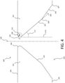
- FIG. 4 is a cross-sectional view of a second embodiment of an extractor 200.
- the extractor 200 includes many of the features of the extractor 100, but the sidewall 103 is divided into a first section 201 and a second section 202 that meet at an angle 204.
- the first section 201 can correspond to the frustoconical aperture 102 from FIG. 1 .
- the second section 202 of the sidewall 103 can form a second frustoconical aperture 203 that widens at a greater rate than the frustoconical aperture 102 as a distance from the first surface 104 increases.
- the first section 201 meets the curved edge 106 and the second section 202 meets the second surface 105.
- the second section 202 may be angled from the first section 201 by an angle 205 from 15° to 45°. This can account for possible misalignments of the extractor 200 relative to an emitter and may prevent excessive electrostatic field leakage caused by a large angle between the first section 201 and the second section 202. A larger or smaller angle 205 between the first section 201 and the second section 202 may be possible.
- FIG. 4 further reduces the possibility of secondary electron generation because the sidewall 103 is angled even farther away from the path of the electron beam, such as that illustrated by the dashed line 109, in the second section 202.
- Additional sections besides the first section 201 and second section 202 are possible. These additional sections also may meet at an angle.
- two of the sections in the extractor 200 may meet at a rounded edge.
- the extractor 200 of FIG. 4 can be used in a scanning electron microscope or other devices that use electron beams.
- FIG. 5 is a view of the extractor 100 of FIG. 1 during an embodiment of operation.
- the tip 500 is misaligned with respect to the center of the frustoconical aperture 102 (represented by the line 501).
- electrons extracted from the tip 500 represented by the lines 502 can still pass through the extractor 100 with minimized generation of secondary electrons.
- the benefit of FIG. 5 can be applicable to the extractor 200 of FIG. 4 as well.
- FIG. 6 is a cross-sectional view of a third embodiment of an extractor system 300 with a first electrode 301, second electrode 302, and third electrode 303.
- the second electrode 302 and third electrode 303 may correspond to the extractor 100 or extractor 200 of FIG. 1 or 4 .
- an electron beam passes through the first electrode 301, second electrode 302, and third electrode 303, such as along the dashed line 320.
- the first electrode 301 has a first surface 304 and opposite second surface 305.
- the first electrode 301 also has a sidewall 306 that defines a cylindrical aperture 307 between the first surface 304 and the second surface 305.
- the cylindrical aperture 307 may have other shapes, such as frustoconical.
- FIG. 6 shows curved edges on the first electrode 301, but the edges also may be beveled.
- the second electrode 302 is disposed adjacent and spaced apart from the first electrode 301.
- the second electrode 302 has a second electrode first surface 308 opposite second electrode second surface 309.
- the second electrode 302 also has a second electrode sidewall 310 that defines a second electrode frustoconical aperture 311 between the second electrode first surface 308 and the second electrode second surface 309.
- the second electrode frustoconical aperture 311 widens from the second electrode first surface 308 to the second electrode second surface 309.
- the second electrode sidewall 310 of the second electrode frustoconical aperture 311 can meet the second electrode first surface 308 at a curved edge 312 and can meet the second electrode second surface 309 at an angled edge 313.
- the second electrode sidewall 310 also can meet the second electrode second surface 309 at a curved edge.
- the third electrode 303 is disposed adjacent and spaced apart from the second electrode 302.
- the third electrode 303 has a third electrode first surface 314 and a third electrode second surface 315 opposite the third electrode first surface 314.
- the third electrode 303 also has a third electrode sidewall 316 that defines a third electrode frustoconical aperture 317 between the third electrode first surface 314 and the third electrode second surface 315.
- the third electrode frustoconical aperture 317 widens from the third electrode first surface 314 to the third electrode second surface 315.
- the third electrode sidewall 316 of the third electrode frustoconical aperture 317 can meet the third electrode first surface 314 at a second curved edge 318 and can meet the third electrode second surface 315 at a second angled edge 319.
- the third electrode sidewall 316 also can meet the third electrode second surface 315 at a curved edge.
- the first electrode 301 and the third electrode 303 are both biased at a first voltage (e.g., V ext ).
- the second electrode 302 is biased at a second voltage (e.g., V ext ⁇ ⁇ V) different from the first voltage.
- secondary electrons may be rejected back to the sidewalls by a negative field with a ⁇ V of approximately negative tens to low hundreds of volts. If ⁇ V is positive tens to low hundreds of volts, then the secondary electrons may be extracted or collected by the second electrode 302. As a result, few or no secondary electrons may exit the extractor system 300 to enter an accelerator region located downstream of the extractor system 300 with respect to a direction of the electron beam.
- the cylindrical aperture 307 of the first electrode 301 has a first diameter 321. This may be at the narrowest point in the cylindrical aperture 307.
- the second electrode frustoconical aperture 311 of the second electrode 302 can have a second diameter 322 at the second electrode first surface 308 and a third diameter 323 at the second electrode second surface 309, which may be at the narrowest and widest points of the second electrode frustoconical aperture 311, respectively.
- the third electrode frustoconical aperture 317 of the third electrode 303 can have a fourth diameter 324 at the third electrode first surface and a fifth diameter 325 at the third electrode second surface 315, which may be at the narrowest and widest points of the third electrode frustoconical aperture 317, respectively.
- the first diameter 321 and the second diameter 322 may be equal.
- the third diameter 323 and the fourth diameter 324 may be equal.
- the fifth diameter 325 may be larger than any of the other diameters. While drawn as equal, other diameters are possible.
- the first diameter 321 may be from 100 ⁇ m to 500 ⁇ m.
- the second diameter 322 may be from 200 ⁇ m to 600 ⁇ m.
- the fourth diameter 324 may be from 300 ⁇ m to 800 ⁇ m.
- the second electrode frustoconical aperture 311 and the third electrode frustoconical aperture 317 may be angled from 15° to 60° and 15° to 60° relative to the dashed line 320 (which may be parallel to a line through the center of the various apertures), respectively.
- the depth of the second electrode frustoconical aperture 311 and third electrode frustoconical aperture 317 may be from 0.3 mm to 2.0 mm, including all values to the 0.1 mm and ranges between.
- the dimensions and angles in the second electrode frustoconical aperture 311 and the third electrode frustoconical aperture 317 may be selected such that the primary beam electrons emitted from the source tip do not bombard their aperture surfaces, even if the tip is misaligned.
- the primary beam electrons may bombard the aperture surface of the first electrode 301 and generate secondary electrons. These secondary electrons can be rejected or extracted by the second electrode 302.
- Other dimensions for the second electrode frustoconical aperture 311 and the third electrode frustoconical aperture 317 are possible because the potential differences between the electrodes are as low as around a hundred Volts. For example, the dimensions may vary by a value from 10 ⁇ m to 50 ⁇ m.
- the radii for the curved edge 312 and second curved edge 318 may be from 10 ⁇ m to 50 ⁇ m. These dimensions may be possible because the fields at the second electrode 302 and third electrode 303 can be relatively small. There may be less concern with minimizing the surface area exposed to the electron beam in the second electrode 302 and third electrode 303 because the extractor system 300 may rely on rejecting or trapping secondary electrons rather than minimizing generation of secondary electrons.
- the radii for curved edges in the first electrode also may be from 10 ⁇ m to 50 ⁇ m. Other radii are possible.
- a suppressor can be disposed adjacent and spaced apart from the first electrode 301 opposite the second electrode 302.
- the extractor system 300 of FIG. 6 can be used in a scanning electron microscope or other devices that use electron beams.
- the extractor system 300 can be retrofitted into existing systems without redesigning the electron emission system.
- the impact of the secondary electrodes can be further minimized using the embodiments disclosed in FIGs. 1-5 .
- a distance between the extractor or extractor system and a subsequent electrode e.g., an electrode downstream of the extractor
- the travel distance of the primary electron beam to the subsequent electrode is shorter, and the primary electron beam travels faster due to the higher acceleration between the electrodes.
- the travel time of the primary electron beam is reduced, along with the interaction time with the secondary electrons.
- the shorter distance between the electrodes can reduce the maximum practical voltage difference between the electrodes, and, therefore, the maximum usable voltage of the electron source.
- the total range of beam current may be reduced. Minimizing the distance may be applicable for various applications.
- the extractor or extractor system may be coated with a material with low secondary electron yield, such as carbon, to further minimize generation of secondary electrons.
- Embodiments of the extractor disclosed herein can be manufactured by micromachining (e.g., drilling), though other techniques are possible.
- Embodiments disclosed herein can be used in an electron source with a magnetic lens, where the interaction time between the primary and secondary electrons is greatest.
- the electron source may include a magnetic immersion lens.
- Embodiments disclosed herein may be implemented as part of an electron source.
- the electron source can operate in the Schottky emission mode, with a combination of high temperature and high electrostatic field at the electron emitter.
- the extractor or extractor system can generate the electrostatic field at the emitter, causing both electron emission from the emitter and acceleration of the electron beam away from the emitter.
- a magnetic lens can focus the primary electron beam as it travels through the electron source. With the optimized design of the extractor or extractor system, in particular the sidewalls, secondary electron generation is minimized and the primary beam is undisturbed. This can enable a high-performance electron source for electron beam inspection and review.
- Such an electron source may need to deliver an electron beam into a very small spot size (e.g., as low as 1-2 nm) over a wide range of beam energy and current. Unless secondary electron generation is minimized, difficult tradeoffs of beam spot size, beam energy range, or beam current range may need to be accepted.
- the embodiments described herein may include or be performed in a system, such as the system 400 of FIG. 7 .
- the system 400 includes an output acquisition subsystem that includes at least an energy source and a detector.
- the output acquisition subsystem may be an electron beam-based output acquisition subsystem.
- the energy directed to the wafer 404 includes electrons
- the energy detected from the wafer 404 includes electrons.
- the energy source may be an electron beam source 402, which can include or be coupled with an extractor or extractor system as disclosed herein.
- the output acquisition subsystem includes electron optical column 401, which is coupled to computer subsystem 407.
- the electron optical column 401 includes electron beam source 402 configured to generate electrons that are focused to wafer 404 by one or more elements 403.
- the electron beam source 402 may include an emitter and one or more elements 403 may include, for example, a gun lens, an anode, a beam limiting aperture, a gate valve, a beam current selection aperture, an objective lens, and/or a scanning subsystem.
- the electron column 401 may include any other suitable elements known in the art. While only one electron beam source 402 is illustrated, the system 400 may include multiple electron beam sources 402.
- Electrons returned from the wafer 404 may be focused by one or more elements 405 to detector 406.
- One or more elements 405 may include, for example, a scanning subsystem, which may be the same scanning subsystem included in element(s) 403.
- the electron column 401 may include any other suitable elements known in the art.
- the electron column 401 is shown in FIG. 7 as being configured such that the electrons are directed to the wafer 404 at an oblique angle of incidence and are scattered from the wafer at another oblique angle, it is to be understood that the electron beam may be directed to and scattered from the wafer at any suitable angle.
- the electron beam-based output acquisition subsystem may be configured to use multiple modes to generate images of the wafer 404 (e.g., with different illumination angles, collection angles, etc.). The multiple modes of the electron beam-based output acquisition subsystem may be different in any image generation parameters of the output acquisition subsystem.
- Computer subsystem 407 may be in electronic communication with the detector 406.
- the detector 406 may detect electrons returned from the surface of the wafer 404 thereby forming electron beam images of the wafer 404.
- the electron beam images may include any suitable electron beam images.
- Computer subsystem 407 may be configured to perform other functions or additional steps using the output of the detector 406 and/or the electron beam images.
- FIG. 7 is provided herein to generally illustrate a configuration of an electron beam-based output acquisition subsystem.
- the electron beam-based output acquisition subsystem configuration described herein may be altered to optimize the performance of the output acquisition subsystem as is normally performed when designing a commercial output acquisition system.
- the systems described herein may be implemented using an existing system (e.g., by adding functionality described herein to an existing system).
- the methods described herein may be provided as optional functionality of the system (e.g., in addition to other functionality of the system).
- the system 400 is an inspection system.
- the electron beam output acquisition subsystems described herein may be configured as inspection systems.
- the system 400 is a defect review system.
- the electron beam output acquisition subsystems described herein may be configured as defect review systems.
- the system 400 is a metrology system.
- the electron beam output acquisition subsystems described herein may be configured as metrology systems.
- the embodiments of the system 400 described herein and shown in FIG. 7 may be modified in one or more parameters to provide different imaging capability depending on the application for which they will be used.
- the system 400 shown in FIG. 7 may be configured to have a higher resolution if it is to be used for defect review or metrology rather than for inspection.
- the embodiment of the system 400 shown in FIG. 7 describes some general and various configurations for a system 400 that can be tailored in a number of manners to produce output acquisition subsystems having different imaging capabilities that are more or less suitable for different applications.
- the embodiments described herein may be installed on a computer node or computer cluster that is a component of or coupled to an output acquisition subsystem such as an electron beam inspector or defect review tool, a mask inspector, a virtual inspector, or other devices.
- an output acquisition subsystem such as an electron beam inspector or defect review tool, a mask inspector, a virtual inspector, or other devices.
- the embodiments described herein may generate output that can be used for a variety of applications that include, but are not limited to, wafer inspection, mask inspection, electron beam inspection and review, metrology, or other applications.
- the characteristics of the system 400 shown in FIG. 7 can be modified as described above based on the specimen for which it will generate output.
- the methods may be performed as described herein.
- the methods also may include any other step(s) that can be performed by the controller and/or computer subsystem(s) or system(s) described herein.
- the steps can be performed by one or more computer systems, which may be configured according to any of the embodiments described herein.
- the methods described above may be performed by any of the system embodiments described herein.
Landscapes
- Chemical & Material Sciences (AREA)
- Analytical Chemistry (AREA)
- Electron Sources, Ion Sources (AREA)
- Cold Cathode And The Manufacture (AREA)
Claims (15)
- Appareil pour une source d'électrons, l'appareil comprenant :
un extracteur étant une électrode d'extracteur (100, 200, 302) ayant une première surface (104) et une seconde surface (105) opposée à la première surface, dans lequel l'extracteur a une paroi latérale (103) qui définit une ouverture tronconique (102) entre la première surface et la seconde surface, dans lequel l'ouverture tronconique s'élargit de la première surface à la seconde surface, dans lequel la paroi latérale de l'ouverture tronconique rencontre la première surface au niveau d'un bord incliné (106) et dans lequel le bord incliné a un rayon (108) de 5 µm à 50 µm. - Appareil selon la revendication 1, comprenant en outre un émetteur d'électrons, dans lequel l'extracteur est positionné en aval de l'émetteur par rapport à une direction d'un faisceau d'électrons.
- Appareil selon la revendication 2, dans lequel l'extracteur est configuré pour générer un champ électrostatique au niveau de l'émetteur provoquant ainsi l'émission et l'accélération d'électrons.
- Appareil selon la revendication 1, dans lequel l'ouverture est centrale par rapport à la première surface de l'extracteur.
- Appareil selon la revendication 1, dans lequel la paroi latérale rencontre la seconde surface au niveau d'un bord incliné.
- Appareil selon la revendication 1, dans lequel la paroi latérale est inclinée par rapport à un centre de l'ouverture tronconique de 5° à 75°.
- Appareil selon la revendication 1, dans lequel l'ouverture tronconique a un diamètre de 100 µm à 500 µm.
- Appareil selon la revendication 1, dans lequel l'ouverture tronconique a une profondeur de 0,3 mm à 2,0 mm.
- Appareil selon la revendication 1, dans lequel l'extracteur fait partie d'une lentille magnétique.
- Appareil selon la revendication 1, dans lequel la paroi latérale définit une première section et une seconde section, dans lequel la première section correspond à l'ouverture tronconique, dans lequel la seconde section définit une seconde ouverture tronconique qui s'élargit à une plus grande vitesse que l'ouverture tronconique et dans lequel la seconde section est disposée sur la première section et rencontre la seconde surface.
- Appareil selon la revendication 1, dans lequel les parois latérales sont revêtues de carbone.
- Microscope électronique à balayage comportant l'appareil selon la revendication 1.
- Système de faisceau d'électrons comprenant :
une source d'électrons qui comporte un émetteur d'électrons et l'appareil selon la revendication 1. - Système de faisceau d'électrons selon la revendication 13, dans lequel la source d'électrons est configurée pour fonctionner dans un mode d'émission Schottky.
- Système de faisceau d'électrons selon la revendication 13, dans lequel l'extracteur fait partie d'une lentille magnétique.
Applications Claiming Priority (3)
| Application Number | Priority Date | Filing Date | Title |
|---|---|---|---|
| US201762447917P | 2017-01-19 | 2017-01-19 | |
| US15/593,900 US9934933B1 (en) | 2017-01-19 | 2017-05-12 | Extractor electrode for electron source |
| PCT/US2018/014560 WO2018136817A1 (fr) | 2017-01-19 | 2018-01-19 | Électrode d'extracteur pour source d'électrons |
Publications (3)
| Publication Number | Publication Date |
|---|---|
| EP3549151A1 EP3549151A1 (fr) | 2019-10-09 |
| EP3549151A4 EP3549151A4 (fr) | 2020-10-28 |
| EP3549151B1 true EP3549151B1 (fr) | 2022-03-09 |
Family
ID=61711655
Family Applications (1)
| Application Number | Title | Priority Date | Filing Date |
|---|---|---|---|
| EP18741046.9A Active EP3549151B1 (fr) | 2017-01-19 | 2018-01-19 | Électrode d'extracteur pour source d'électrons |
Country Status (8)
| Country | Link |
|---|---|
| US (1) | US9934933B1 (fr) |
| EP (1) | EP3549151B1 (fr) |
| JP (1) | JP6947831B2 (fr) |
| KR (1) | KR102343210B1 (fr) |
| CN (1) | CN110192262B (fr) |
| IL (1) | IL267816B (fr) |
| TW (1) | TWI742226B (fr) |
| WO (1) | WO2018136817A1 (fr) |
Families Citing this family (4)
| Publication number | Priority date | Publication date | Assignee | Title |
|---|---|---|---|---|
| US11302510B2 (en) | 2018-05-29 | 2022-04-12 | Kla-Tencor Corporation | Space charge insensitive electron gun designs |
| US12451319B2 (en) | 2020-10-05 | 2025-10-21 | Kla Corporation | Electron source with magnetic suppressor electrode |
| US11508591B2 (en) * | 2021-02-08 | 2022-11-22 | Kla Corporation | High resolution electron beam apparatus with dual-aperture schemes |
| US11869743B2 (en) * | 2021-05-11 | 2024-01-09 | Kla Corporation | High throughput multi-electron beam system |
Family Cites Families (31)
| Publication number | Priority date | Publication date | Assignee | Title |
|---|---|---|---|---|
| US3585546A (en) * | 1969-10-21 | 1971-06-15 | Jeol Ltd | Objective lens pole pieces |
| DD237932B1 (de) * | 1985-05-31 | 1988-06-22 | Ardenne Forschungsinst | Elektronenkanone fuer hohe strahlleistungen |
| FR2641899A1 (fr) * | 1989-01-17 | 1990-07-20 | Thomson Tubes Electroniques | Canon a electrons muni d'un dispositif actif produisant un champ magnetique au voisinage de la cathode |
| US5199917A (en) * | 1991-12-09 | 1993-04-06 | Cornell Research Foundation, Inc. | Silicon tip field emission cathode arrays and fabrication thereof |
| JPH06318436A (ja) * | 1993-03-05 | 1994-11-15 | Hitachi Ltd | 受像管 |
| JPH07230773A (ja) * | 1994-02-16 | 1995-08-29 | Mitsubishi Electric Corp | 陰極線管用電子銃およびそのグリッド電極の製造方法 |
| US5828064A (en) * | 1995-08-11 | 1998-10-27 | Philips Electronics North America Corporation | Field emission environmental scanning electron microscope |
| DE19638109A1 (de) * | 1995-09-25 | 1997-03-27 | Jeol Ltd | Elektronenstrahl-Lithographie-System |
| JPH10112274A (ja) * | 1996-08-12 | 1998-04-28 | Nikon Corp | 電子銃 |
| JPH11354007A (ja) * | 1998-06-11 | 1999-12-24 | Hitachi Ltd | 電子源およびそれを用いた電子線装置 |
| GB2347686B (en) * | 1999-03-08 | 2003-06-11 | Trikon Holdings Ltd | Gas delivery system |
| ATE438922T1 (de) * | 2000-03-16 | 2009-08-15 | Hitachi Ltd | Vorrichtung zum erzeugen eines stromes von ladungsträgern |
| US7259378B2 (en) * | 2003-04-10 | 2007-08-21 | Applied Process Technologies, Inc. | Closed drift ion source |
| US7892357B2 (en) * | 2004-01-12 | 2011-02-22 | Axcelis Technologies, Inc. | Gas distribution plate assembly for plasma reactors |
| JP4445893B2 (ja) * | 2005-04-06 | 2010-04-07 | 株式会社日立ハイテクノロジーズ | 走査形電子顕微鏡 |
| JP2007080704A (ja) * | 2005-09-15 | 2007-03-29 | Mie Univ | 電界放出型電子銃およびその電源電圧制御方法 |
| KR101384260B1 (ko) * | 2005-12-05 | 2014-04-11 | 전자빔기술센터 주식회사 | 전자칼럼의 전자빔 포커싱 방법 |
| JP2008053226A (ja) * | 2006-07-26 | 2008-03-06 | Mamoru Nakasuji | 電子銃及び電子線装置 |
| WO2008147846A1 (fr) * | 2007-05-22 | 2008-12-04 | Semequip, Inc. | Procédé et système permettant d'extraire des faisceaux d'ions composés d'ions moléculaires (système d'extraction de faisceaux d'ions en agrégats) |
| US7888640B2 (en) * | 2007-06-18 | 2011-02-15 | Hitachi High-Technologies Corporation | Scanning electron microscope and method of imaging an object by using the scanning electron microscope |
| JP5277250B2 (ja) * | 2008-09-25 | 2013-08-28 | 株式会社日立ハイテクノロジーズ | 荷電粒子線応用装置およびその幾何収差測定方法 |
| WO2010070837A1 (fr) * | 2008-12-16 | 2010-06-24 | 株式会社日立ハイテクノロジーズ | Dispositif à faisceau électronique et dispositif d'application de faisceau électronique l'utilisant |
| JP5178926B2 (ja) * | 2010-02-08 | 2013-04-10 | 株式会社日立ハイテクノロジーズ | 荷電粒子顕微鏡及びイオン顕微鏡 |
| JP5948084B2 (ja) * | 2012-02-28 | 2016-07-06 | 株式会社日立ハイテクノロジーズ | 走査電子顕微鏡 |
| TWI638241B (zh) * | 2012-03-26 | 2018-10-11 | 日商尼康股份有限公司 | 基板處理裝置、處理裝置及元件製造方法 |
| US8513619B1 (en) * | 2012-05-10 | 2013-08-20 | Kla-Tencor Corporation | Non-planar extractor structure for electron source |
| JP6340165B2 (ja) * | 2013-04-25 | 2018-06-06 | 株式会社日立ハイテクノロジーズ | 電子銃、荷電粒子銃およびそれらを用いた荷電粒子線装置 |
| WO2014181685A1 (fr) * | 2013-05-10 | 2014-11-13 | 株式会社日立ハイテクノロジーズ | Dispositif à faisceau de particules chargées |
| CN203351940U (zh) * | 2013-07-01 | 2013-12-18 | 海信容声(广东)冰箱有限公司 | 一种负离子器、负离子风装置及冰箱除臭装置 |
| US9384937B2 (en) * | 2013-09-27 | 2016-07-05 | Varian Semiconductor Equipment Associates, Inc. | SiC coating in an ion implanter |
| US9406535B2 (en) * | 2014-08-29 | 2016-08-02 | Lam Research Corporation | Ion injector and lens system for ion beam milling |
-
2017
- 2017-05-12 US US15/593,900 patent/US9934933B1/en active Active
-
2018
- 2018-01-18 TW TW107101805A patent/TWI742226B/zh active
- 2018-01-19 CN CN201880007432.1A patent/CN110192262B/zh active Active
- 2018-01-19 WO PCT/US2018/014560 patent/WO2018136817A1/fr not_active Ceased
- 2018-01-19 JP JP2019538471A patent/JP6947831B2/ja active Active
- 2018-01-19 KR KR1020197023765A patent/KR102343210B1/ko active Active
- 2018-01-19 IL IL267816A patent/IL267816B/en unknown
- 2018-01-19 EP EP18741046.9A patent/EP3549151B1/fr active Active
Also Published As
| Publication number | Publication date |
|---|---|
| WO2018136817A1 (fr) | 2018-07-26 |
| JP2020505728A (ja) | 2020-02-20 |
| CN110192262B (zh) | 2020-11-10 |
| TW201841184A (zh) | 2018-11-16 |
| IL267816B (en) | 2022-09-01 |
| EP3549151A1 (fr) | 2019-10-09 |
| JP6947831B2 (ja) | 2021-10-13 |
| IL267816A (en) | 2019-09-26 |
| TWI742226B (zh) | 2021-10-11 |
| EP3549151A4 (fr) | 2020-10-28 |
| US9934933B1 (en) | 2018-04-03 |
| KR20190102080A (ko) | 2019-09-02 |
| KR102343210B1 (ko) | 2021-12-23 |
| CN110192262A (zh) | 2019-08-30 |
Similar Documents
| Publication | Publication Date | Title |
|---|---|---|
| KR102373865B1 (ko) | 하전 입자 빔 시료 검사 시스템 및 그 동작 방법 | |
| US6825475B2 (en) | Deflection method and system for use in a charged particle beam column | |
| EP2801997B1 (fr) | Système d'inspection de tranche par faisceau d'électrons et son procédé de fonctionnement | |
| US7067807B2 (en) | Charged particle beam column and method of its operation | |
| EP2511939B1 (fr) | Agencement et procédé pour l'amélioration du contraste dans un dispositif pour l'inspection d'un spécimen avec un faisceau de particules chargées | |
| EP3549151B1 (fr) | Électrode d'extracteur pour source d'électrons | |
| EP2896062B1 (fr) | Appareil d'émission de faisceaux d'électrons à canon d'électrons à deux lentilles pour l'imagerie haute résolution à forts et faibles courants de faisceau | |
| CN115398591B (zh) | 用于3d装置的检验及检视的电子束系统 | |
| EP2219204B1 (fr) | Agencement et procédé pour l'amélioration du contraste dans un dispositif à faisceau de particules chargées pour l'inspection d'un spécimen | |
| TW202006779A (zh) | 高效能檢查掃描電子顯微鏡裝置及其操作方法 | |
| CN101322218B (zh) | 用于在电子柱中聚焦电子束的方法 | |
| EP4324012A1 (fr) | Appareil à faisceau d'électrons multiples à haute résolution | |
| US10446360B2 (en) | Particle source for producing a particle beam and particle-optical apparatus | |
| US10734191B2 (en) | Charged particle beam device | |
| EP3467866A1 (fr) | Dispositif avec colonne ionique et microscope électronique à balayage | |
| US7233008B1 (en) | Multiple electrode lens arrangement and a method for inspecting an object | |
| US11961704B2 (en) | Charged particle beam system | |
| US20250046562A1 (en) | Objective lens and charged particle beam apparatus including same | |
| JP7570527B2 (ja) | デュアルアパーチャ方式の高解像度電子ビーム装置 | |
| US20020079449A1 (en) | SEM having a detector surface segmented into a number of separate regions |
Legal Events
| Date | Code | Title | Description |
|---|---|---|---|
| STAA | Information on the status of an ep patent application or granted ep patent |
Free format text: STATUS: THE INTERNATIONAL PUBLICATION HAS BEEN MADE |
|
| PUAI | Public reference made under article 153(3) epc to a published international application that has entered the european phase |
Free format text: ORIGINAL CODE: 0009012 |
|
| STAA | Information on the status of an ep patent application or granted ep patent |
Free format text: STATUS: REQUEST FOR EXAMINATION WAS MADE |
|
| 17P | Request for examination filed |
Effective date: 20190704 |
|
| AK | Designated contracting states |
Kind code of ref document: A1 Designated state(s): AL AT BE BG CH CY CZ DE DK EE ES FI FR GB GR HR HU IE IS IT LI LT LU LV MC MK MT NL NO PL PT RO RS SE SI SK SM TR |
|
| AX | Request for extension of the european patent |
Extension state: BA ME |
|
| DAV | Request for validation of the european patent (deleted) | ||
| DAX | Request for extension of the european patent (deleted) | ||
| REG | Reference to a national code |
Ref country code: DE Ref legal event code: R079 Ref document number: 602018031999 Country of ref document: DE Free format text: PREVIOUS MAIN CLASS: H01J0037073000 Ipc: H01J0037065000 |
|
| A4 | Supplementary search report drawn up and despatched |
Effective date: 20200924 |
|
| RIC1 | Information provided on ipc code assigned before grant |
Ipc: H01J 37/065 20060101AFI20200918BHEP Ipc: H01J 37/28 20060101ALI20200918BHEP Ipc: H01J 37/073 20060101ALI20200918BHEP |
|
| GRAP | Despatch of communication of intention to grant a patent |
Free format text: ORIGINAL CODE: EPIDOSNIGR1 |
|
| STAA | Information on the status of an ep patent application or granted ep patent |
Free format text: STATUS: GRANT OF PATENT IS INTENDED |
|
| INTG | Intention to grant announced |
Effective date: 20210929 |
|
| RIN1 | Information on inventor provided before grant (corrected) |
Inventor name: CUMMINGS, KEVIN Inventor name: FLORENDO, OSCAR G. Inventor name: BUI, DANIEL Inventor name: SEARS, CHRISTOPHER Inventor name: JIANG, XINRONG Inventor name: CHUBUN, NIKOLAI Inventor name: GRELLA, LUCA Inventor name: HORDON, LAURENCE S. |
|
| GRAS | Grant fee paid |
Free format text: ORIGINAL CODE: EPIDOSNIGR3 |
|
| GRAA | (expected) grant |
Free format text: ORIGINAL CODE: 0009210 |
|
| STAA | Information on the status of an ep patent application or granted ep patent |
Free format text: STATUS: THE PATENT HAS BEEN GRANTED |
|
| AK | Designated contracting states |
Kind code of ref document: B1 Designated state(s): AL AT BE BG CH CY CZ DE DK EE ES FI FR GB GR HR HU IE IS IT LI LT LU LV MC MK MT NL NO PL PT RO RS SE SI SK SM TR |
|
| REG | Reference to a national code |
Ref country code: CH Ref legal event code: EP Ref country code: AT Ref legal event code: REF Ref document number: 1474849 Country of ref document: AT Kind code of ref document: T Effective date: 20220315 |
|
| REG | Reference to a national code |
Ref country code: IE Ref legal event code: FG4D |
|
| REG | Reference to a national code |
Ref country code: DE Ref legal event code: R096 Ref document number: 602018031999 Country of ref document: DE |
|
| REG | Reference to a national code |
Ref country code: NL Ref legal event code: FP |
|
| REG | Reference to a national code |
Ref country code: LT Ref legal event code: MG9D |
|
| PG25 | Lapsed in a contracting state [announced via postgrant information from national office to epo] |
Ref country code: SE Free format text: LAPSE BECAUSE OF FAILURE TO SUBMIT A TRANSLATION OF THE DESCRIPTION OR TO PAY THE FEE WITHIN THE PRESCRIBED TIME-LIMIT Effective date: 20220309 Ref country code: RS Free format text: LAPSE BECAUSE OF FAILURE TO SUBMIT A TRANSLATION OF THE DESCRIPTION OR TO PAY THE FEE WITHIN THE PRESCRIBED TIME-LIMIT Effective date: 20220309 Ref country code: NO Free format text: LAPSE BECAUSE OF FAILURE TO SUBMIT A TRANSLATION OF THE DESCRIPTION OR TO PAY THE FEE WITHIN THE PRESCRIBED TIME-LIMIT Effective date: 20220609 Ref country code: LT Free format text: LAPSE BECAUSE OF FAILURE TO SUBMIT A TRANSLATION OF THE DESCRIPTION OR TO PAY THE FEE WITHIN THE PRESCRIBED TIME-LIMIT Effective date: 20220309 Ref country code: HR Free format text: LAPSE BECAUSE OF FAILURE TO SUBMIT A TRANSLATION OF THE DESCRIPTION OR TO PAY THE FEE WITHIN THE PRESCRIBED TIME-LIMIT Effective date: 20220309 Ref country code: BG Free format text: LAPSE BECAUSE OF FAILURE TO SUBMIT A TRANSLATION OF THE DESCRIPTION OR TO PAY THE FEE WITHIN THE PRESCRIBED TIME-LIMIT Effective date: 20220609 |
|
| REG | Reference to a national code |
Ref country code: AT Ref legal event code: MK05 Ref document number: 1474849 Country of ref document: AT Kind code of ref document: T Effective date: 20220309 |
|
| PG25 | Lapsed in a contracting state [announced via postgrant information from national office to epo] |
Ref country code: LV Free format text: LAPSE BECAUSE OF FAILURE TO SUBMIT A TRANSLATION OF THE DESCRIPTION OR TO PAY THE FEE WITHIN THE PRESCRIBED TIME-LIMIT Effective date: 20220309 Ref country code: GR Free format text: LAPSE BECAUSE OF FAILURE TO SUBMIT A TRANSLATION OF THE DESCRIPTION OR TO PAY THE FEE WITHIN THE PRESCRIBED TIME-LIMIT Effective date: 20220610 Ref country code: FI Free format text: LAPSE BECAUSE OF FAILURE TO SUBMIT A TRANSLATION OF THE DESCRIPTION OR TO PAY THE FEE WITHIN THE PRESCRIBED TIME-LIMIT Effective date: 20220309 |
|
| PG25 | Lapsed in a contracting state [announced via postgrant information from national office to epo] |
Ref country code: SM Free format text: LAPSE BECAUSE OF FAILURE TO SUBMIT A TRANSLATION OF THE DESCRIPTION OR TO PAY THE FEE WITHIN THE PRESCRIBED TIME-LIMIT Effective date: 20220309 Ref country code: SK Free format text: LAPSE BECAUSE OF FAILURE TO SUBMIT A TRANSLATION OF THE DESCRIPTION OR TO PAY THE FEE WITHIN THE PRESCRIBED TIME-LIMIT Effective date: 20220309 Ref country code: RO Free format text: LAPSE BECAUSE OF FAILURE TO SUBMIT A TRANSLATION OF THE DESCRIPTION OR TO PAY THE FEE WITHIN THE PRESCRIBED TIME-LIMIT Effective date: 20220309 Ref country code: PT Free format text: LAPSE BECAUSE OF FAILURE TO SUBMIT A TRANSLATION OF THE DESCRIPTION OR TO PAY THE FEE WITHIN THE PRESCRIBED TIME-LIMIT Effective date: 20220711 Ref country code: ES Free format text: LAPSE BECAUSE OF FAILURE TO SUBMIT A TRANSLATION OF THE DESCRIPTION OR TO PAY THE FEE WITHIN THE PRESCRIBED TIME-LIMIT Effective date: 20220309 Ref country code: EE Free format text: LAPSE BECAUSE OF FAILURE TO SUBMIT A TRANSLATION OF THE DESCRIPTION OR TO PAY THE FEE WITHIN THE PRESCRIBED TIME-LIMIT Effective date: 20220309 Ref country code: CZ Free format text: LAPSE BECAUSE OF FAILURE TO SUBMIT A TRANSLATION OF THE DESCRIPTION OR TO PAY THE FEE WITHIN THE PRESCRIBED TIME-LIMIT Effective date: 20220309 Ref country code: AT Free format text: LAPSE BECAUSE OF FAILURE TO SUBMIT A TRANSLATION OF THE DESCRIPTION OR TO PAY THE FEE WITHIN THE PRESCRIBED TIME-LIMIT Effective date: 20220309 |
|
| PG25 | Lapsed in a contracting state [announced via postgrant information from national office to epo] |
Ref country code: PL Free format text: LAPSE BECAUSE OF FAILURE TO SUBMIT A TRANSLATION OF THE DESCRIPTION OR TO PAY THE FEE WITHIN THE PRESCRIBED TIME-LIMIT Effective date: 20220309 Ref country code: IS Free format text: LAPSE BECAUSE OF FAILURE TO SUBMIT A TRANSLATION OF THE DESCRIPTION OR TO PAY THE FEE WITHIN THE PRESCRIBED TIME-LIMIT Effective date: 20220709 Ref country code: AL Free format text: LAPSE BECAUSE OF FAILURE TO SUBMIT A TRANSLATION OF THE DESCRIPTION OR TO PAY THE FEE WITHIN THE PRESCRIBED TIME-LIMIT Effective date: 20220309 |
|
| REG | Reference to a national code |
Ref country code: DE Ref legal event code: R097 Ref document number: 602018031999 Country of ref document: DE |
|
| PLBE | No opposition filed within time limit |
Free format text: ORIGINAL CODE: 0009261 |
|
| STAA | Information on the status of an ep patent application or granted ep patent |
Free format text: STATUS: NO OPPOSITION FILED WITHIN TIME LIMIT |
|
| PG25 | Lapsed in a contracting state [announced via postgrant information from national office to epo] |
Ref country code: DK Free format text: LAPSE BECAUSE OF FAILURE TO SUBMIT A TRANSLATION OF THE DESCRIPTION OR TO PAY THE FEE WITHIN THE PRESCRIBED TIME-LIMIT Effective date: 20220309 |
|
| 26N | No opposition filed |
Effective date: 20221212 |
|
| PG25 | Lapsed in a contracting state [announced via postgrant information from national office to epo] |
Ref country code: SI Free format text: LAPSE BECAUSE OF FAILURE TO SUBMIT A TRANSLATION OF THE DESCRIPTION OR TO PAY THE FEE WITHIN THE PRESCRIBED TIME-LIMIT Effective date: 20220309 |
|
| P01 | Opt-out of the competence of the unified patent court (upc) registered |
Effective date: 20230525 |
|
| PG25 | Lapsed in a contracting state [announced via postgrant information from national office to epo] |
Ref country code: IT Free format text: LAPSE BECAUSE OF FAILURE TO SUBMIT A TRANSLATION OF THE DESCRIPTION OR TO PAY THE FEE WITHIN THE PRESCRIBED TIME-LIMIT Effective date: 20220309 |
|
| REG | Reference to a national code |
Ref country code: CH Ref legal event code: PL |
|
| GBPC | Gb: european patent ceased through non-payment of renewal fee |
Effective date: 20230119 |
|
| PG25 | Lapsed in a contracting state [announced via postgrant information from national office to epo] |
Ref country code: LU Free format text: LAPSE BECAUSE OF NON-PAYMENT OF DUE FEES Effective date: 20230119 |
|
| REG | Reference to a national code |
Ref country code: BE Ref legal event code: MM Effective date: 20230131 |
|
| PG25 | Lapsed in a contracting state [announced via postgrant information from national office to epo] |
Ref country code: LI Free format text: LAPSE BECAUSE OF NON-PAYMENT OF DUE FEES Effective date: 20230131 Ref country code: GB Free format text: LAPSE BECAUSE OF NON-PAYMENT OF DUE FEES Effective date: 20230119 Ref country code: CH Free format text: LAPSE BECAUSE OF NON-PAYMENT OF DUE FEES Effective date: 20230131 |
|
| PG25 | Lapsed in a contracting state [announced via postgrant information from national office to epo] |
Ref country code: FR Free format text: LAPSE BECAUSE OF NON-PAYMENT OF DUE FEES Effective date: 20230131 Ref country code: BE Free format text: LAPSE BECAUSE OF NON-PAYMENT OF DUE FEES Effective date: 20230131 |
|
| PG25 | Lapsed in a contracting state [announced via postgrant information from national office to epo] |
Ref country code: IE Free format text: LAPSE BECAUSE OF NON-PAYMENT OF DUE FEES Effective date: 20230119 |
|
| PG25 | Lapsed in a contracting state [announced via postgrant information from national office to epo] |
Ref country code: MC Free format text: LAPSE BECAUSE OF FAILURE TO SUBMIT A TRANSLATION OF THE DESCRIPTION OR TO PAY THE FEE WITHIN THE PRESCRIBED TIME-LIMIT Effective date: 20220309 |
|
| PG25 | Lapsed in a contracting state [announced via postgrant information from national office to epo] |
Ref country code: MC Free format text: LAPSE BECAUSE OF FAILURE TO SUBMIT A TRANSLATION OF THE DESCRIPTION OR TO PAY THE FEE WITHIN THE PRESCRIBED TIME-LIMIT Effective date: 20220309 |
|
| PG25 | Lapsed in a contracting state [announced via postgrant information from national office to epo] |
Ref country code: CY Free format text: LAPSE BECAUSE OF FAILURE TO SUBMIT A TRANSLATION OF THE DESCRIPTION OR TO PAY THE FEE WITHIN THE PRESCRIBED TIME-LIMIT; INVALID AB INITIO Effective date: 20180119 |
|
| PG25 | Lapsed in a contracting state [announced via postgrant information from national office to epo] |
Ref country code: HU Free format text: LAPSE BECAUSE OF FAILURE TO SUBMIT A TRANSLATION OF THE DESCRIPTION OR TO PAY THE FEE WITHIN THE PRESCRIBED TIME-LIMIT; INVALID AB INITIO Effective date: 20180119 |
|
| PG25 | Lapsed in a contracting state [announced via postgrant information from national office to epo] |
Ref country code: TR Free format text: LAPSE BECAUSE OF FAILURE TO SUBMIT A TRANSLATION OF THE DESCRIPTION OR TO PAY THE FEE WITHIN THE PRESCRIBED TIME-LIMIT Effective date: 20220309 |
|
| PGFP | Annual fee paid to national office [announced via postgrant information from national office to epo] |
Ref country code: NL Payment date: 20260126 Year of fee payment: 9 |
|
| PGFP | Annual fee paid to national office [announced via postgrant information from national office to epo] |
Ref country code: DE Payment date: 20260128 Year of fee payment: 9 |