EP3567591B1 - Mémoire à accès aléatoire et circuit, procédé et système associés - Google Patents
Mémoire à accès aléatoire et circuit, procédé et système associés Download PDFInfo
- Publication number
- EP3567591B1 EP3567591B1 EP19182004.2A EP19182004A EP3567591B1 EP 3567591 B1 EP3567591 B1 EP 3567591B1 EP 19182004 A EP19182004 A EP 19182004A EP 3567591 B1 EP3567591 B1 EP 3567591B1
- Authority
- EP
- European Patent Office
- Prior art keywords
- node
- connects
- transistor
- gate
- voltage
- Prior art date
- Legal status (The legal status is an assumption and is not a legal conclusion. Google has not performed a legal analysis and makes no representation as to the accuracy of the status listed.)
- Not-in-force
Links
Images






Classifications
-
- G—PHYSICS
- G11—INFORMATION STORAGE
- G11C—STATIC STORES
- G11C11/00—Digital stores characterised by the use of particular electric or magnetic storage elements; Storage elements therefor
- G11C11/21—Digital stores characterised by the use of particular electric or magnetic storage elements; Storage elements therefor using electric elements
- G11C11/34—Digital stores characterised by the use of particular electric or magnetic storage elements; Storage elements therefor using electric elements using semiconductor devices
- G11C11/40—Digital stores characterised by the use of particular electric or magnetic storage elements; Storage elements therefor using electric elements using semiconductor devices using transistors
- G11C11/41—Digital stores characterised by the use of particular electric or magnetic storage elements; Storage elements therefor using electric elements using semiconductor devices using transistors forming static cells with positive feedback, i.e. cells not needing refreshing or charge regeneration, e.g. bistable multivibrator or Schmitt trigger
- G11C11/413—Auxiliary circuits, e.g. for addressing, decoding, driving, writing, sensing, timing or power reduction
-
- G—PHYSICS
- G11—INFORMATION STORAGE
- G11C—STATIC STORES
- G11C11/00—Digital stores characterised by the use of particular electric or magnetic storage elements; Storage elements therefor
- G11C11/21—Digital stores characterised by the use of particular electric or magnetic storage elements; Storage elements therefor using electric elements
- G11C11/34—Digital stores characterised by the use of particular electric or magnetic storage elements; Storage elements therefor using electric elements using semiconductor devices
- G11C11/40—Digital stores characterised by the use of particular electric or magnetic storage elements; Storage elements therefor using electric elements using semiconductor devices using transistors
- G11C11/41—Digital stores characterised by the use of particular electric or magnetic storage elements; Storage elements therefor using electric elements using semiconductor devices using transistors forming static cells with positive feedback, i.e. cells not needing refreshing or charge regeneration, e.g. bistable multivibrator or Schmitt trigger
- G11C11/413—Auxiliary circuits, e.g. for addressing, decoding, driving, writing, sensing, timing or power reduction
- G11C11/417—Auxiliary circuits, e.g. for addressing, decoding, driving, writing, sensing, timing or power reduction for memory cells of the field-effect type
- G11C11/419—Read-write [R-W] circuits
-
- G—PHYSICS
- G11—INFORMATION STORAGE
- G11C—STATIC STORES
- G11C11/00—Digital stores characterised by the use of particular electric or magnetic storage elements; Storage elements therefor
- G11C11/21—Digital stores characterised by the use of particular electric or magnetic storage elements; Storage elements therefor using electric elements
- G11C11/34—Digital stores characterised by the use of particular electric or magnetic storage elements; Storage elements therefor using electric elements using semiconductor devices
- G11C11/40—Digital stores characterised by the use of particular electric or magnetic storage elements; Storage elements therefor using electric elements using semiconductor devices using transistors
- G11C11/41—Digital stores characterised by the use of particular electric or magnetic storage elements; Storage elements therefor using electric elements using semiconductor devices using transistors forming static cells with positive feedback, i.e. cells not needing refreshing or charge regeneration, e.g. bistable multivibrator or Schmitt trigger
- G11C11/413—Auxiliary circuits, e.g. for addressing, decoding, driving, writing, sensing, timing or power reduction
- G11C11/417—Auxiliary circuits, e.g. for addressing, decoding, driving, writing, sensing, timing or power reduction for memory cells of the field-effect type
-
- G—PHYSICS
- G11—INFORMATION STORAGE
- G11C—STATIC STORES
- G11C11/00—Digital stores characterised by the use of particular electric or magnetic storage elements; Storage elements therefor
- G11C11/21—Digital stores characterised by the use of particular electric or magnetic storage elements; Storage elements therefor using electric elements
- G11C11/34—Digital stores characterised by the use of particular electric or magnetic storage elements; Storage elements therefor using electric elements using semiconductor devices
- G11C11/40—Digital stores characterised by the use of particular electric or magnetic storage elements; Storage elements therefor using electric elements using semiconductor devices using transistors
- G11C11/401—Digital stores characterised by the use of particular electric or magnetic storage elements; Storage elements therefor using electric elements using semiconductor devices using transistors forming cells needing refreshing or charge regeneration, i.e. dynamic cells
- G11C11/403—Digital stores characterised by the use of particular electric or magnetic storage elements; Storage elements therefor using electric elements using semiconductor devices using transistors forming cells needing refreshing or charge regeneration, i.e. dynamic cells with charge regeneration common to a multiplicity of memory cells, i.e. external refresh
- G11C11/405—Digital stores characterised by the use of particular electric or magnetic storage elements; Storage elements therefor using electric elements using semiconductor devices using transistors forming cells needing refreshing or charge regeneration, i.e. dynamic cells with charge regeneration common to a multiplicity of memory cells, i.e. external refresh with three charge-transfer gates, e.g. MOS transistors, per cell
-
- G—PHYSICS
- G11—INFORMATION STORAGE
- G11C—STATIC STORES
- G11C11/00—Digital stores characterised by the use of particular electric or magnetic storage elements; Storage elements therefor
- G11C11/21—Digital stores characterised by the use of particular electric or magnetic storage elements; Storage elements therefor using electric elements
- G11C11/34—Digital stores characterised by the use of particular electric or magnetic storage elements; Storage elements therefor using electric elements using semiconductor devices
- G11C11/40—Digital stores characterised by the use of particular electric or magnetic storage elements; Storage elements therefor using electric elements using semiconductor devices using transistors
- G11C11/401—Digital stores characterised by the use of particular electric or magnetic storage elements; Storage elements therefor using electric elements using semiconductor devices using transistors forming cells needing refreshing or charge regeneration, i.e. dynamic cells
- G11C11/406—Management or control of the refreshing or charge-regeneration cycles
-
- G—PHYSICS
- G11—INFORMATION STORAGE
- G11C—STATIC STORES
- G11C11/00—Digital stores characterised by the use of particular electric or magnetic storage elements; Storage elements therefor
- G11C11/21—Digital stores characterised by the use of particular electric or magnetic storage elements; Storage elements therefor using electric elements
- G11C11/34—Digital stores characterised by the use of particular electric or magnetic storage elements; Storage elements therefor using electric elements using semiconductor devices
- G11C11/40—Digital stores characterised by the use of particular electric or magnetic storage elements; Storage elements therefor using electric elements using semiconductor devices using transistors
- G11C11/401—Digital stores characterised by the use of particular electric or magnetic storage elements; Storage elements therefor using electric elements using semiconductor devices using transistors forming cells needing refreshing or charge regeneration, i.e. dynamic cells
- G11C11/4063—Auxiliary circuits, e.g. for addressing, decoding, driving, writing, sensing or timing
- G11C11/407—Auxiliary circuits, e.g. for addressing, decoding, driving, writing, sensing or timing for memory cells of the field-effect type
- G11C11/4074—Power supply or voltage generation circuits, e.g. bias voltage generators, substrate voltage generators, back-up power, power control circuits
-
- G—PHYSICS
- G11—INFORMATION STORAGE
- G11C—STATIC STORES
- G11C11/00—Digital stores characterised by the use of particular electric or magnetic storage elements; Storage elements therefor
- G11C11/21—Digital stores characterised by the use of particular electric or magnetic storage elements; Storage elements therefor using electric elements
- G11C11/34—Digital stores characterised by the use of particular electric or magnetic storage elements; Storage elements therefor using electric elements using semiconductor devices
- G11C11/40—Digital stores characterised by the use of particular electric or magnetic storage elements; Storage elements therefor using electric elements using semiconductor devices using transistors
- G11C11/401—Digital stores characterised by the use of particular electric or magnetic storage elements; Storage elements therefor using electric elements using semiconductor devices using transistors forming cells needing refreshing or charge regeneration, i.e. dynamic cells
- G11C11/4063—Auxiliary circuits, e.g. for addressing, decoding, driving, writing, sensing or timing
- G11C11/407—Auxiliary circuits, e.g. for addressing, decoding, driving, writing, sensing or timing for memory cells of the field-effect type
- G11C11/4076—Timing circuits
-
- G—PHYSICS
- G11—INFORMATION STORAGE
- G11C—STATIC STORES
- G11C11/00—Digital stores characterised by the use of particular electric or magnetic storage elements; Storage elements therefor
- G11C11/21—Digital stores characterised by the use of particular electric or magnetic storage elements; Storage elements therefor using electric elements
- G11C11/34—Digital stores characterised by the use of particular electric or magnetic storage elements; Storage elements therefor using electric elements using semiconductor devices
- G11C11/40—Digital stores characterised by the use of particular electric or magnetic storage elements; Storage elements therefor using electric elements using semiconductor devices using transistors
- G11C11/401—Digital stores characterised by the use of particular electric or magnetic storage elements; Storage elements therefor using electric elements using semiconductor devices using transistors forming cells needing refreshing or charge regeneration, i.e. dynamic cells
- G11C11/4063—Auxiliary circuits, e.g. for addressing, decoding, driving, writing, sensing or timing
- G11C11/407—Auxiliary circuits, e.g. for addressing, decoding, driving, writing, sensing or timing for memory cells of the field-effect type
- G11C11/408—Address circuits
-
- G—PHYSICS
- G11—INFORMATION STORAGE
- G11C—STATIC STORES
- G11C11/00—Digital stores characterised by the use of particular electric or magnetic storage elements; Storage elements therefor
- G11C11/21—Digital stores characterised by the use of particular electric or magnetic storage elements; Storage elements therefor using electric elements
- G11C11/34—Digital stores characterised by the use of particular electric or magnetic storage elements; Storage elements therefor using electric elements using semiconductor devices
- G11C11/40—Digital stores characterised by the use of particular electric or magnetic storage elements; Storage elements therefor using electric elements using semiconductor devices using transistors
- G11C11/401—Digital stores characterised by the use of particular electric or magnetic storage elements; Storage elements therefor using electric elements using semiconductor devices using transistors forming cells needing refreshing or charge regeneration, i.e. dynamic cells
- G11C11/4063—Auxiliary circuits, e.g. for addressing, decoding, driving, writing, sensing or timing
- G11C11/407—Auxiliary circuits, e.g. for addressing, decoding, driving, writing, sensing or timing for memory cells of the field-effect type
- G11C11/408—Address circuits
- G11C11/4085—Word line control circuits, e.g. word line drivers, - boosters, - pull-up, - pull-down, - precharge
-
- G—PHYSICS
- G11—INFORMATION STORAGE
- G11C—STATIC STORES
- G11C11/00—Digital stores characterised by the use of particular electric or magnetic storage elements; Storage elements therefor
- G11C11/21—Digital stores characterised by the use of particular electric or magnetic storage elements; Storage elements therefor using electric elements
- G11C11/34—Digital stores characterised by the use of particular electric or magnetic storage elements; Storage elements therefor using electric elements using semiconductor devices
- G11C11/40—Digital stores characterised by the use of particular electric or magnetic storage elements; Storage elements therefor using electric elements using semiconductor devices using transistors
- G11C11/401—Digital stores characterised by the use of particular electric or magnetic storage elements; Storage elements therefor using electric elements using semiconductor devices using transistors forming cells needing refreshing or charge regeneration, i.e. dynamic cells
- G11C11/4063—Auxiliary circuits, e.g. for addressing, decoding, driving, writing, sensing or timing
- G11C11/407—Auxiliary circuits, e.g. for addressing, decoding, driving, writing, sensing or timing for memory cells of the field-effect type
- G11C11/408—Address circuits
- G11C11/4087—Address decoders, e.g. bit - or word line decoders; Multiple line decoders
-
- G—PHYSICS
- G11—INFORMATION STORAGE
- G11C—STATIC STORES
- G11C11/00—Digital stores characterised by the use of particular electric or magnetic storage elements; Storage elements therefor
- G11C11/21—Digital stores characterised by the use of particular electric or magnetic storage elements; Storage elements therefor using electric elements
- G11C11/34—Digital stores characterised by the use of particular electric or magnetic storage elements; Storage elements therefor using electric elements using semiconductor devices
- G11C11/40—Digital stores characterised by the use of particular electric or magnetic storage elements; Storage elements therefor using electric elements using semiconductor devices using transistors
- G11C11/401—Digital stores characterised by the use of particular electric or magnetic storage elements; Storage elements therefor using electric elements using semiconductor devices using transistors forming cells needing refreshing or charge regeneration, i.e. dynamic cells
- G11C11/4063—Auxiliary circuits, e.g. for addressing, decoding, driving, writing, sensing or timing
- G11C11/407—Auxiliary circuits, e.g. for addressing, decoding, driving, writing, sensing or timing for memory cells of the field-effect type
- G11C11/409—Read-write [R-W] circuits
-
- G—PHYSICS
- G11—INFORMATION STORAGE
- G11C—STATIC STORES
- G11C11/00—Digital stores characterised by the use of particular electric or magnetic storage elements; Storage elements therefor
- G11C11/21—Digital stores characterised by the use of particular electric or magnetic storage elements; Storage elements therefor using electric elements
- G11C11/34—Digital stores characterised by the use of particular electric or magnetic storage elements; Storage elements therefor using electric elements using semiconductor devices
- G11C11/40—Digital stores characterised by the use of particular electric or magnetic storage elements; Storage elements therefor using electric elements using semiconductor devices using transistors
- G11C11/401—Digital stores characterised by the use of particular electric or magnetic storage elements; Storage elements therefor using electric elements using semiconductor devices using transistors forming cells needing refreshing or charge regeneration, i.e. dynamic cells
- G11C11/4063—Auxiliary circuits, e.g. for addressing, decoding, driving, writing, sensing or timing
- G11C11/407—Auxiliary circuits, e.g. for addressing, decoding, driving, writing, sensing or timing for memory cells of the field-effect type
- G11C11/409—Read-write [R-W] circuits
- G11C11/4093—Input/output [I/O] data interface arrangements, e.g. data buffers
-
- G—PHYSICS
- G11—INFORMATION STORAGE
- G11C—STATIC STORES
- G11C11/00—Digital stores characterised by the use of particular electric or magnetic storage elements; Storage elements therefor
- G11C11/21—Digital stores characterised by the use of particular electric or magnetic storage elements; Storage elements therefor using electric elements
- G11C11/34—Digital stores characterised by the use of particular electric or magnetic storage elements; Storage elements therefor using electric elements using semiconductor devices
- G11C11/40—Digital stores characterised by the use of particular electric or magnetic storage elements; Storage elements therefor using electric elements using semiconductor devices using transistors
- G11C11/401—Digital stores characterised by the use of particular electric or magnetic storage elements; Storage elements therefor using electric elements using semiconductor devices using transistors forming cells needing refreshing or charge regeneration, i.e. dynamic cells
- G11C11/4063—Auxiliary circuits, e.g. for addressing, decoding, driving, writing, sensing or timing
- G11C11/407—Auxiliary circuits, e.g. for addressing, decoding, driving, writing, sensing or timing for memory cells of the field-effect type
- G11C11/409—Read-write [R-W] circuits
- G11C11/4094—Bit-line management or control circuits
-
- G—PHYSICS
- G11—INFORMATION STORAGE
- G11C—STATIC STORES
- G11C11/00—Digital stores characterised by the use of particular electric or magnetic storage elements; Storage elements therefor
- G11C11/21—Digital stores characterised by the use of particular electric or magnetic storage elements; Storage elements therefor using electric elements
- G11C11/34—Digital stores characterised by the use of particular electric or magnetic storage elements; Storage elements therefor using electric elements using semiconductor devices
- G11C11/40—Digital stores characterised by the use of particular electric or magnetic storage elements; Storage elements therefor using electric elements using semiconductor devices using transistors
- G11C11/401—Digital stores characterised by the use of particular electric or magnetic storage elements; Storage elements therefor using electric elements using semiconductor devices using transistors forming cells needing refreshing or charge regeneration, i.e. dynamic cells
- G11C11/4063—Auxiliary circuits, e.g. for addressing, decoding, driving, writing, sensing or timing
- G11C11/407—Auxiliary circuits, e.g. for addressing, decoding, driving, writing, sensing or timing for memory cells of the field-effect type
- G11C11/409—Read-write [R-W] circuits
- G11C11/4096—Input/output [I/O] data management or control circuits, e.g. reading or writing circuits, I/O drivers or bit-line switches
-
- G—PHYSICS
- G11—INFORMATION STORAGE
- G11C—STATIC STORES
- G11C11/00—Digital stores characterised by the use of particular electric or magnetic storage elements; Storage elements therefor
- G11C11/21—Digital stores characterised by the use of particular electric or magnetic storage elements; Storage elements therefor using electric elements
- G11C11/34—Digital stores characterised by the use of particular electric or magnetic storage elements; Storage elements therefor using electric elements using semiconductor devices
- G11C11/40—Digital stores characterised by the use of particular electric or magnetic storage elements; Storage elements therefor using electric elements using semiconductor devices using transistors
- G11C11/41—Digital stores characterised by the use of particular electric or magnetic storage elements; Storage elements therefor using electric elements using semiconductor devices using transistors forming static cells with positive feedback, i.e. cells not needing refreshing or charge regeneration, e.g. bistable multivibrator or Schmitt trigger
- G11C11/412—Digital stores characterised by the use of particular electric or magnetic storage elements; Storage elements therefor using electric elements using semiconductor devices using transistors forming static cells with positive feedback, i.e. cells not needing refreshing or charge regeneration, e.g. bistable multivibrator or Schmitt trigger using field-effect transistors only
-
- G—PHYSICS
- G11—INFORMATION STORAGE
- G11C—STATIC STORES
- G11C11/00—Digital stores characterised by the use of particular electric or magnetic storage elements; Storage elements therefor
- G11C11/21—Digital stores characterised by the use of particular electric or magnetic storage elements; Storage elements therefor using electric elements
- G11C11/34—Digital stores characterised by the use of particular electric or magnetic storage elements; Storage elements therefor using electric elements using semiconductor devices
- G11C11/40—Digital stores characterised by the use of particular electric or magnetic storage elements; Storage elements therefor using electric elements using semiconductor devices using transistors
- G11C11/41—Digital stores characterised by the use of particular electric or magnetic storage elements; Storage elements therefor using electric elements using semiconductor devices using transistors forming static cells with positive feedback, i.e. cells not needing refreshing or charge regeneration, e.g. bistable multivibrator or Schmitt trigger
- G11C11/413—Auxiliary circuits, e.g. for addressing, decoding, driving, writing, sensing, timing or power reduction
- G11C11/417—Auxiliary circuits, e.g. for addressing, decoding, driving, writing, sensing, timing or power reduction for memory cells of the field-effect type
- G11C11/418—Address circuits
-
- G—PHYSICS
- G11—INFORMATION STORAGE
- G11C—STATIC STORES
- G11C5/00—Details of stores covered by group G11C11/00
- G11C5/14—Power supply arrangements, e.g. power down, chip selection or deselection, layout of wirings or power grids, or multiple supply levels
- G11C5/147—Voltage reference generators, voltage or current regulators; Internally lowered supply levels; Compensation for voltage drops
-
- G—PHYSICS
- G11—INFORMATION STORAGE
- G11C—STATIC STORES
- G11C7/00—Arrangements for writing information into, or reading information out from, a digital store
- G11C7/10—Input/output [I/O] data interface arrangements, e.g. I/O data control circuits, I/O data buffers
- G11C7/1006—Data managing, e.g. manipulating data before writing or reading out, data bus switches or control circuits therefor
-
- G—PHYSICS
- G11—INFORMATION STORAGE
- G11C—STATIC STORES
- G11C7/00—Arrangements for writing information into, or reading information out from, a digital store
- G11C7/10—Input/output [I/O] data interface arrangements, e.g. I/O data control circuits, I/O data buffers
- G11C7/1051—Data output circuits, e.g. read-out amplifiers, data output buffers, data output registers, data output level conversion circuits
- G11C7/106—Data output latches
-
- G—PHYSICS
- G11—INFORMATION STORAGE
- G11C—STATIC STORES
- G11C7/00—Arrangements for writing information into, or reading information out from, a digital store
- G11C7/10—Input/output [I/O] data interface arrangements, e.g. I/O data control circuits, I/O data buffers
- G11C7/1051—Data output circuits, e.g. read-out amplifiers, data output buffers, data output registers, data output level conversion circuits
- G11C7/1069—I/O lines read out arrangements
-
- G—PHYSICS
- G11—INFORMATION STORAGE
- G11C—STATIC STORES
- G11C7/00—Arrangements for writing information into, or reading information out from, a digital store
- G11C7/10—Input/output [I/O] data interface arrangements, e.g. I/O data control circuits, I/O data buffers
- G11C7/1078—Data input circuits, e.g. write amplifiers, data input buffers, data input registers, data input level conversion circuits
- G11C7/1087—Data input latches
-
- G—PHYSICS
- G11—INFORMATION STORAGE
- G11C—STATIC STORES
- G11C7/00—Arrangements for writing information into, or reading information out from, a digital store
- G11C7/10—Input/output [I/O] data interface arrangements, e.g. I/O data control circuits, I/O data buffers
- G11C7/1078—Data input circuits, e.g. write amplifiers, data input buffers, data input registers, data input level conversion circuits
- G11C7/1096—Write circuits, e.g. I/O line write drivers
-
- G—PHYSICS
- G11—INFORMATION STORAGE
- G11C—STATIC STORES
- G11C7/00—Arrangements for writing information into, or reading information out from, a digital store
- G11C7/12—Bit line control circuits, e.g. drivers, boosters, pull-up circuits, pull-down circuits, precharging circuits, equalising circuits, for bit lines
-
- G—PHYSICS
- G11—INFORMATION STORAGE
- G11C—STATIC STORES
- G11C2211/00—Indexing scheme relating to digital stores characterized by the use of particular electric or magnetic storage elements; Storage elements therefor
- G11C2211/401—Indexing scheme relating to cells needing refreshing or charge regeneration, i.e. dynamic cells
- G11C2211/406—Refreshing of dynamic cells
- G11C2211/4066—Pseudo-SRAMs
Definitions
- the present invention relates to a memory element of a random-access memory, and more particularly, to semiconductor process technologies capable of implementing static random-access memories and dynamic random-access memories, and further capable of implementing the corresponding access circuits and access systems.
- DRAM Dynamic Random-Access Memory
- US Patent No. 4,802,129 teaches a pulse for enabling a write driver before a read can be performed, the system must recover from a write.
- a write signal terminates, the data input signal will still be valid for some time.
- the pre-charging circuit comprises a pair of transistors.
- an output circuit When the memory is in a read mode, an output circuit generates an output signal which represents a logic state on data lines.
- an input circuit drives data lines to a logic state representing the logic state of an input signal.
- a write enable pulse is generated in response to a change in a logic state of the input signal.
- a data transition pulse is provided, which is delayed in time from the write enable pulse.
- US Patent Application No. 2009/168,559 details a circuit which detects a data transition of a data signal and generates a pulse signal in response.
- the pulse is a trigger for capturing the data signal.
- the present invention aims at providing a DRAM with standard semiconductor process technology, its structure consisting of one transistor and one diode, wherein the depletion capacitance of the diode is utilized to form a capacitor. Furthermore, it can cooperate with an access circuit corresponding to an SRAM. The performance is thus enhanced.
- the present invention reduces the number of used transistors for elevating the integrated intensity for an SRAM; preferably, only three transistors will be used in standard CMOS process technology to implement an SRAM for overcoming the stability of storage status and reducing the power consumption of the memory. Further, related circuits and the corresponding access circuit and system will be implemented.
- the CPU has a cache memory whose hardware circuit is implemented by an SRAM.
- SRAM static random access memory
- the present invention is not limited to solving the aforementioned problems. Those skilled in the art should understand that the advantages and characteristic of the limited teaching taught by the present invention can be applied to related products in the future, or replace the memory products relevant to the related art.
- exemplary means “as example, implementation or interpretation”. As described as “exemplary”, any embodiment should not be interpreted as an embodiment better than others or with more advantages.
- hierarchical circuit mentioned in the following paragraphs is used to describe a circuit diagram and/or a block diagram, which is a well-known design method in the electronic circuit field and the integrated circuit field.
- terminal point means a terminal point of the supply voltage, or the supply voltage may connect or couple to the terminal point.
- node means the supply voltage and any signal might couple between the hierarchy where the circuit positioned in and the last hierarchy, the farther hierarchy or the first hierarchy.
- the specific circuit is positioned in one of the hierarchies in the hierarchical circuit, and it may couple to other elements or circuits beyond the hierarchy where the specific circuit is positioned. After the coupling, the hierarchy where the specific circuit is positioned becomes the next hierarchy. Furthermore, different circuit diagrams might use the same node name, but the node might couple to other places.
- the term "connective point” mentioned in the following paragraphs means a metal connecting point for physical connection between the electrical elements or electronic circuits.
- MOSFET Metal Oxide Semiconductor Field Effect Transistor
- N-type MOSFET and P-type MOSFET these are indicated as NMOS and PMOS, respectively, in the following.
- a symbol of MOSFET with four nodes comprises a source terminal, a drain terminal, a gate terminal and a bulk; the source terminal should be marked by an arrow, if not, it should be easily recognized.
- Another symbol of MOSFET with three nodes comprises a source terminal, a drain terminal and a gate terminal; the source terminal should be marked by an arrow, if not, it should be easily recognized, wherein the bulk without additional mark means it is directly connected to the source terminal.
- CMOS process technology a bulk can be grouped into P-type substrate and N-type substrate, wherein the p-type substrate is commonly used. Therefore, when the N-type substrate is applied, the aforementioned NMOS needs to be replaced by PMOS, and vice versa. In addition, the terminal point originally coupled to the supply voltage needs to couple to the ground instead, and vice versa.
- SRAM cell Static Random-Access Memory cell
- FIG. 1 which shows an SRAM cell 100 consisting of five transistors under transistor-level design, which will be referred to as "5T SRAM cell” in the following.
- M1 to M5 are MOSFETs respectively defined as first to fifth transistors, wherein M1, M4 and M5 are each an NMOS while M2 and M3 are each a PMOS. Said transistors form a storage cell, and M1 is also called the access transistor.
- Bit Line is a data node arranged to input or output a bit data value.
- Word Line hereinafter "WL”
- WL is an address node arranged to control writing or reading said bit data value.
- An input node A supply voltage of cell, stated as "Vcell", is a cell power terminal point which accepts a suitable voltage to perform a write or read operation.
- the 5T SRAM cell 100 comprises a data transmission node, a transmission control node, a cell power terminal point, a ground terminal point, a first transistor, a second transistor, a third transistor, a fourth transistor, and a fifth transistor.
- the wiring net of said memory element is shown in FIG. 1 which is a well-known prior art. The detailed description is omitted.
- the 5T SRAM cell is a prior art memory element, wherein a first inverter consists of M2 and M4, and a second inverter consists of M3 and M5. Said first inverter and said second inverter are used to latch data by feedback connection.
- a first inverter consists of M2 and M4
- a second inverter consists of M3 and M5.
- Said first inverter and said second inverter are used to latch data by feedback connection.
- FIG. 2 which shows an SRAM cell 100 consisting of four transistors under transistor-level design, which will be referred to as "4T SRAM cell” in the following.
- M21 to M24 are MOSFETs respectively defined as first to fourth transistor, wherein M21 and M24 are each an NMOS while M22 and M23 are each a PMOS.
- the other nodes are similar to those in FIG. 1 .
- the 4T SRAM cell 100 comprises a data transmission node, a transmission control node, a cell power terminal point, a ground terminal point, a first transistor, a second transistor, a third transistor, and a fourth transistor.
- the wiring net of said memory element is shown in FIG. 2 which is well-known in the prior art. The detailed description is omitted.
- the 4T SRAM cell is a Single-Rail-and-Robust Memory, wherein a logic level has strong stability while another has weak stability.
- the retention of the 4T SRAM cell relies on leakage current of the transistors.
- M23 When M23 is cut off, there will still be a leakage current between the source terminal and drain terminal of M23. Said current flows to the source terminal of M21 from the drain terminal, then finally to the ground terminal point via BL.
- the leakage current and bulk current of M21 and the working current of M23 constitute a first current path, wherein said first current path equals a first inverter; the working current of M4 and working current of M22 constitute a second current path, and M24 is dynamically controlled causing a strong pull-low current.
- Said second current path equals a second inverter; said first inverter and said second inverter are used to latch data by a feedback connection.
- FIG. 3 shows an SRAM cell 100 consisting of three transistors and one resistor under transistor-level design, which will be stated as “3T1R SRAM cell” in the following.
- M31 to M33 are MOSFETs respectively stated as first to third transistors, wherein M31 is an NMOS, while M32 and M33 are each a PMOS, and R1 is a resistor comprising a first connective point and a second connective point. Said transistors and said resistor form a storage cell.
- the other nodes are similar to those in FIG. 1 and FIG. 2 .
- the 3T1R SRAM cell 100 comprises a data transmission node, a transmission control node, a cell power terminal point, a ground terminal point, a first transistor, a second transistor, a third transistor, and a first resistor.
- the wiring net of said memory element is shown in FIG. 3 and is well-known in the prior art. The detailed description is omitted.
- the retention of the 3T1R SRAM cell not only relies on leakage current of the transistor to stabilize said bit data value, but also the resistance of R1 for cooperating with dynamical variation of M32. Because M32 has low resistance when turned on but has high resistance when cut off, resistance of R1 cannot be too high or too low. It is hard for standard CMOS process technology to manufacture a resistor with high resistance. The 3T1R SRAM cell, therefore, is hard to be implemented in standard process technology. When M31 is turned on, said storage cell rapidly loses the ability of latching data.
- leakage current and bulk current of M31 and working current of M33 constitute a first current path, wherein said first current path equals a first inverter; the current passing through R1 and working current of M32 constitute a second current path, and there is also a middle pull-low current, wherein said second current path equals a second inverter; said first inverter and said second inverter are arranged to latch data by feedback connection.
- the detailed interpretation can be known by referring to the journal "5/2012, "The technique problem of 3T SRAM has a solution by taking advantage of CMOS", New Electronic Technology”.
- FIG. 4 shows an SRAM cell 100 consisting of three transistors and one diode under transistor-level design, which will be referred to as "3T1D SRAM cell” in the following.
- M41 to M43 are MOSFETs respectively stated as first to third transistors, wherein M41 is an NMOS while M42 and M43 are each a PMOS, and D1 is a diode comprising an anode and a cathode.
- the anode is called a first connective point and the cathode is called a second connective point.
- the other nodes are similar to those in FIG. 1 - FIG. 3.
- the 3T1D SRAM cell 100 comprises a data transmission node, a transmission control node, a cell power terminal point, a ground terminal point, a first transistor, a second transistor, a third transistor, and a first diode.
- the wiring net of said first transistor is described as follows: the source terminal couples to said data transmission node; the gate terminal couples to said transmission control node; the drain terminal connects to gate terminal of said second transistor and drain terminal of said third transistor; and the bulk connects to said ground terminal point.
- the wiring net of said second transistor is described as follows: the source terminal connects to said cell power terminal point; the gate terminal connects to drain terminals of said first and said third transistors; and the drain terminal connects to gate terminal of said third transistor and second connective point of said first diode.
- the wiring net of said third transistor is described as follows: the source terminal connects to said cell power terminal point; the gate terminal connects to drain terminal of said second transistor and second connective point of said first diode; and the drain terminal connects to drain terminal of said first transistor and gate terminal of said second transistor.
- the wiring net of said first diode is described as follows: the first connective point connects to said ground terminal point; and the second connective point connects to drain terminal of said second transistor and gate terminal of said third transistor.
- 3T1D SRAM cell is different from the 5T SRAM cell, 4T SRAM cell and 3T1R SRAM cell as mentioned above.
- the difference is caused by said first diode, wherein the wiring net of D1 generates a reverse current which is a weak current and affected by temperature.
- M42 and M43 vary according to the reverse current of D1: for example, the special process parameters such as the thickness of gate oxide.
- M42 and M43 are implemented by another standard process technology to change the transistor type: for example, a transistor with high threshold voltage. Accordingly, when M41 is varied based on the variation of M42 and M43, power consumption of the cell will be reduced. When M41 is turned on, said storage cell rapidly loses the ability of latching data.
- leakage current and bulk current of M41 and working current of M43 constitute a first current path, wherein said first current path equals a first inverter; reverse current of D1 and working current of M42 constitute a second current path, and there is a weak pull-low current, wherein said second current path equals a second inverter; said first inverter and said second inverter are arranged to latch data by a feedback connection.
- CMOS process technology can manufacture several diode types such as "n+/p-well”, “p+/n-well”, “n-well/p-sub” and “ESD”, wherein D1 has a limitation for layout area, and also has to correspond to the current difference resulting from the variation of M42 and M43 due to temperature. Therefore, the most use of diode type is "n+/p-well” in general situation which has a smaller layout area and a better stability.
- a varactor may be used to stand high operating temperature.
- an SRAM cell 100 is consisting of three transistors and one capacitor under transistor-level design, which will be stated as "3T1C SRAM cell” in the following. Please note that this embodiment will be easier to implemented by Silicon-On-Insulator (SOI) process technology, and the produced transistor has no bulk.
- M51 to M53 are a MOSFET respectively stated as first to third transistor, wherein M51 is an NMOS while M52 and M53 are a PMOS, and C1 is a capacitor comprising a first connective point and a second connective point.
- the other nodes are similar with those in FIG. 1-FIG.4 .
- the 3T1C SRAM cell comprises a data transmission node, a transmission control node, a cell power terminal point, a ground terminal point, a first transistor, a second transistor, a third transistor, and a first capacitor.
- the connection can be known by referring to the aforementioned 3T1D SRAM cell 100; the detailed description is omitted here.
- the 3T1C SRAM cell has more low leakage current due to the SOI process technology. Therefore, reducing the oxide thickness of C1 might increase direct tunneling current.
- This adjustment is arranged for matching leakage current of said transistors and direct tunneling current of said capacitor as mentioned in the 3T1D SRAM cell.
- the type and the parameter of the transistors can be designed based on the type and the parameters of the diodes to improve the performance, reduce consumed area or minimize the power consumption after reading those embodiments above; apparently, the type and the parameter of the transistors can also be designed based on the type and the parameters of the capacitors.
- a normal voltage a writing voltage, a reading voltage and a standby voltage
- normal voltage is arranged to maintain storage status of the memory element when there is no data being accessed
- writing voltage is arranged to reduce time of status transformation when data is written into the memory element
- reading voltage is arranged to enhance signal strength when data is read from the memory element
- standby voltage is arranged to reduce power consumption.
- the voltage level of these voltages acceptable for the 5T SRAM cell, 4T SRAM cell and 3T1R SRAM cell are described as follows: said reading voltage is higher than or equals said normal voltage, said normal voltage is higher than or equals said writing voltage, and said writing voltage is higher than or equals said standby voltage.
- the 3T1D SRAM cell and 3T1C SRAM cell fully rely on leakage current of transistor to maintain storage status of the memory element. Therefore, the working voltage cannot be too weak, or there is not enough leakage current to maintain storage status of the memory element. However, to destroy storage status of the memory element when writing data, so the voltage level of acceptable working voltages is described as follows: said reading voltage is higher than or equals said normal voltage, said normal voltage is higher than or equals said standby voltage, and said standby voltage is higher than or equals said writing voltage.
- aforementioned memory elements can be slightly changed to implement the dual-port access. For example, a data transmission node, a transmission control node and a transistor may be additionally added; said transistor is also the access transistor.
- the Cell Access and Hold is a type of access circuit, comprising a hold circuit which is positioned between aforementioned memory element and memory transmission interface, and is arranged to write a bit value into aforementioned memory element, or read a bit value from aforementioned memory element.
- said bit value stored in aforementioned memory element is held according to the characteristic of aforementioned memory element.
- FIG. 6 is an exemplary circuit diagram, wherein the Cell Access and Hold 300 (CAH 300) is a circuit diagram combining transistor-level design, gate-level design and function blocks.
- M61 and M62 are a MOSFET respectively stated as first and second transistor, wherein M61 is NMOS while M62 is PMOS.
- Tri1 is tri-state gate; Not61 is NOT gate.
- the CAH 300 can detect a slight variation in voltage via the SPT4_SRAM 301.
- SPT_SRAM 301 is a function block diagram, arranged to detect BL. When BL is slightly increased to high voltage from a relatively low voltage, a rail-to-rail high voltage is quickly outputted. This will be discussed in the following paragraphs.
- "Goad” is a first input connective point
- "Width” is a first output connective point
- "pull” is a second output connective point.
- An input node: Cell Write, hereinafter “CWr” is a control node arranged to start function of cell write, and change storage status of aforementioned memory element.
- An input node: Cell Hold, hereafter “CHd” is a control node arranged to start function of cell hold, and maintain storage status of aforementioned memory element.
- Bit-To-Cell hereinafter "BTC”
- BTC Bit-To-Cell
- BTD Bit-To-Data
- BTC Bit-To-Cell
- BTD Bit-To-Data
- M62 in the CAH 300 is an optional element for 5T/4T SRAM cell, however, it is necessary for 3T1R/3T1D/3T1C SRAM cell, because aforementioned memory element might be influenced by the neighborhood writing to change storage status, which is the most significant difference between 3T1R/3T1D/3T1C SRAM cell and 5T/4T SRAM cell.
- M62 in the CAH 300 is an optional element for 5T/4T SRAM cell, however, it is necessary for 3T1R/3T1D/3T1C SRAM cell, because aforementioned memory element might be influenced by the neighborhood reading to change storage status, furthermore, it may happen destructive readout. These are the most significant differences between 3T1R/3T1D/3T1C SRAM cell and 5T/4T SRAM cell.
- this embodiment is a preferable embodiment, those skilled in the art should understand those electrical elements can be separated from and further coupled to the cell access circuit according to actual design consideration.
- M61 in CAH 300 is necessary for aforementioned memory elements because the key point for aforementioned elements being able to implement data storage is using leakage current of transistor to maintain storage status.
- M61 For the 5T SRAM cell, the existence of M61 can enhance the stability after it enters standby; for 4T/3T1R/3T1D/3T1C SRAM cell, M61 is the necessary element.
- signal waveform of CHd is not a limitation of present invention, wherein in a simple embodiment, M61 is constantly driven, but in the situation for storage status is not being destroyed immediately, M61 can be driven intermittently, or even be driven based on practical situation.
- a circuit of CAH 300 comprises (but is not limited to) a first control node, a second control node, a first data node, a second data node, a data transmission node, a power terminal point, a ground terminal point, a first tri-state gate, a first NOT gate, a first function circuit, a first transistor, and a second transistor.
- said first control node keeps disabling function of cell write, and said second node keeps enabling function of cell hold. At this period, it is in the phase of cell hold, wherein said second control node drives said first transistor to complete cell hold operation.
- said second control node disables function of cell hold, and said first control node enables function of cell write.
- the working phase of cell write is entered.
- step two data value of said first data node is sent to said data transmission node, then cell write operation is completed.
- said first control node disables function of cell write first, and said second control node enables function of cell hold. The working phase of cell hold is entered.
- said second control node keeps enabling function of cell hold. At this period, it is in the working phase of cell hold, wherein said second control node drives said first transistor to complete cell hold operation.
- said second control node disables function of cell hold after the working phase of cell read is entered. To avoid destructive readout, disabling function of cell hold should be executed immediately.
- said second data node receives data value of said data transmission node, and then cell read operation is completed.
- step three said second control node enables function of cell hold after cell read is completed. The working phase of cell hold is thus retained afterward. To avoid the destructive readout, enabling function of cell hold should be executed immediately.
- the circuit of CAH and the corresponding method disclosed by the present invention should cooperate with aforementioned SRAM cell 100, wherein methods of writing and reading may correspond to the same access circuit, but may correspond to different access circuits on the other hand.
- the type of memory elements for said circuit and the corresponding methods cooperate with is not limited in the present invention. If other memory elements have similar characteristics with aforementioned SRAM cell 100, they can be directly applied or be slightly adjusted according to its characteristic.
- the circuit and the corresponding method can be designed according to the characteristic of a DRAM cell. Using the circuit of CAH to read a DRAM cell can complete rewrite operation during reading period. In this way, the Write-After-Read architecture can be removed.
- the DRAM cell may be implemented by 1T1C, 1T-SOI or by using a depletion capacitance of diode to complete 1T1D.
- the depletion capacitance is smaller and said reverse current influenced by the temperature occurs, however, a storage benefit can be owned when the access technique proposed by the present invention is applied.
- the transistor in said cells can adjust some process parameters.
- said cells may use transistor with high threshold voltage to reduce leakage current.
- the circuit disclosed by the present invention still can use transistor with low threshold voltage without elevating supply voltage for BL and WL.
- the storage status of said cell maintains at the logic level.
- the storage status of said cell gradually changes to the first logic level, wherein the first logic level and the second logic level correspond to logic values '0' and '1', respectively; wherein the logic 0 may be a voltage level lower than the trigger level, and the logic 1 may be a voltage level higher than or equal to the trigger level.
- a spread pulse trigger will sense the storage status and then read it out, when the storage status is sensed that is the second logic level, a rewrite operation will be performed immediately; otherwise (if the storage status is not the second logic level), the rewrite operation will not be performed.
- M61 can be replaced with a PMOS in order to match the voltage polarization of the storage status.
- M62 can be replaced with an NMOS in order to match the voltage polarization of rewriting.
- a DRAM cell may be composed of an NMOS and a capacitor.
- M61 shown in FIG. 6 can be replaced with a PMOS, and may make M61 generate pull-high current to compensate the leakage current of the NMOS, in order to obtain longer data retention time, wherein M62 is implemented with a PMOS according to the voltage polarization of the rewrite voltage.
- the Spread Pulse Trigger hereinafter "SPT" is arranged to regard a voltage variation or a pulse with as a trigger to generate a pulse signal of rail-to-rail; wherein, the voltage variation can smaller than the threshold voltage of transistor, the minimum voltage variation is close to zero, and the narrowest pulse width may smaller than a propagation delay of transistor. More specifically, when the voltage of the input node increases to a trigger level from low voltage level, or on the contrary, decreases to the trigger level from high voltage. In other words, the trigger signal is triggered when the voltage level on the input node changes to a second voltage level from a first logic level, then the logic level on the output node is quickly and greatly switched.
- a pulse signal of rail-to-rail is outputted, the pulse width of said pulse signal is bigger than or equal to a propagation delay of transistors.
- the logic level is defined as the input voltage level or the output voltage level of a digital circuit
- the second voltage level is defined as a voltage value different from the first logic level and its voltage polarity is contrary to that of the first logic level.
- the internal circuit in SPT before being improved, generates a pulse signal of rail-to-tail, and output waveform of said circuit is generated by transforming time of said trigger signal into corresponding pulse width, therefore, it is marked as "SPT_W".
- the exemplary waveforms can be referred to FIG. 21 and FIG. 22 .
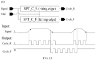
- a clock signal of rail-to-rail is generated, wherein output waveform of said circuit is generated by cyclically producing pulse signals based on time of said trigger signal, therefore, it is marked as "SPT_C".
- the exemplary waveform can be referred to in FIG. 23 .
- those skilled in the art should understand the relation between SPT_W and SPT_C after reading the teachings of the present invention, and understand that it is possible to add a control signal and a switching circuit to comprise both functions to select outputting a width waveform or a cyclical waveform, which is marked as "SPT_B”.
- the detailed explanation and waveform can be referred to the journal "07/2006, "Spread Pulse Trigger and ADC simulation technique", Electronic and Computer, 87".
- Seesaw 200 is a function diagram arranged to switch the logic level quickly and greatly, and is also called a Level Switcher (LS). The detailed description will be discussed in the follow paragraphs. Seesaw 200 comprises a first input connective point and a first output connective point which name is "Poise”.
- the delay 204 is a delay element arranged to delay the transforming time, comprising: a first input connective point and a first output connective which name is "out”.
- time of falling-edge transformation i.e. time from high to low
- is delayed which can be implemented by a Falling-edge Delay Turner. This can be referred to the journal "09/2005, "Logic Gate Design Developing Platform", New Electronic Technology, 234".
- An input node Goad, which is a signal node for taking the slight voltage variation as the trigger level.
- Width which is a signal node for outputting a pulse signal of rail-to-rail generated by transforming time of the trigger signal into the corresponding pulse width.
- the circuit of SPT_W 201 at least comprises a first input node, a first output node, a first LS, a first NOT gate, and a first OR gate, wherein said first LS comprises a first input connective point, a first output connective point, and selectively comprises at least a delay element comprising a first input connective point and a first output connective point.
- the wiring net of said first LS is described as follows: the first input connective point couples to said first input node and first input connective point of said first OR gate; the first output connective point connects to first input connective point of said first NOT gate, and couples to first output connective point of said first OR gate, and selectively connects to first output connective point of said delay element.
- the wiring net of said first NOT gate is described as follows: the first input connective point connects to first output connective point of said first LS, and couples to first output connective point of said first OR gate, and selectively connected to first output connective point of said delay element; the first output connective point couples to second input connective point of said first OR gate and said first output node.
- the wiring net of said first OR gate is described as follows: the first input connective point couples to said first input node and first input connective point of said first LS; the second input connective point couples to first output connective point of said first NOT gate; and the first output connective point couples to first output connective point of said first LS and first input connective point of said first NOT gate, and selectively connects to first input connective point of said delay element.
- the wiring net of said delay element is described as follows: the first input connective point connects to first output connective point of said first OR gate; the first output connective point connects to first output connective point of said first LS and first input connective point of said first NOT gate.
- SPT_W 201 detects the trigger level and generates a pulse signal of rail-to-rail, wherein the first logic level is different and contrary to the second logic level, and the third logic level is different and contrary to the fourth logic level.
- the definition of the second voltage value is a voltage different from the first logic level and its voltage polarity is contrary to that of the first logic level.
- said first input node (Goad) holds on the first logic level
- said first LS outputs the first logic level while said first NOT gate outputs the second logic to make said first OR gate output the second logic level.
- the output connective point of said first LS and the output connective point of said first OR gate constitute a wired-AND therefore said first NOT gate constantly outputs the second logic level.
- Said first output node (Width) holds on the third logic level.
- step one said first input node changes to the second voltage value from the first logic level, or changes back to the first logic level in a predetermined period after being on the second voltage value.
- step two said first LS detects the variation of the first input node, then switches the first logic level to the second logic level instantly, and outputs the second logic level.
- step three said first NOT gate affected by the wired-AND therefore switches the second logic level to the first logic level while said first output node is switched to the fourth logic level from the third logic level.
- step four if said first input node is located on the second logic level, said first OR gate is located on the second logic level, said delay element is located on the second logic level, said first NOT gate is located on the first logic level, and said first output node is located on the fourth logic level.
- step five after said first input node changes back to the first logic level, said first NOT gate outputs the second logic level after said delay element turns back to the first logic level, said first output node outputs the third logic level after said first LS turns back to the first logic level, then the function of spreading pulse width is completed.
- FIG. 8 is an exemplary circuit diagram not part of the invention combining gate-level design and function diagrams, wherein Not81 and Not82 are NOT gates.
- An output node which is a signal node for outputting a clock signal of rail-to-rail generated by cyclically producing pulse signals based on time of the trigger signal.
- the other nodes are similar with those in the above embodiment.
- the circuit of SPT_C 202 at least comprises a first input node, a first output node, a first LS, a first NOT gate, and a delay element, wherein said first LS comprises a first input connective point, a first output connective point, and said delay element comprises a first input connective point and a first output connective point.
- the wiring net of said first LS is described as follows: the first input connective point couples to said first input node; the first output connective point connects to first input connective point of said first NOT gate and first output connective point of said delay element.
- the wiring net of said first NOT gate is described as follows: the first input connective point connects to first output connective point of said first LS and first output connective point of said delay element; the first output connective point couples to first input connective point of said delay element and said first output node.
- the wiring net of said delay element is described as follows: the first input connective point couples to first output connective point of said NOT gate; the first output connective point connects to first output connective point of said first LS and first input connective point of said first NOT gate.
- SPT_C 202 detects the trigger level and generates a clock signal of rail-to-rail, wherein the definition of the first logic level, the second logic level, the third logic level, the fourth logic level, and the second voltage value are same as the SPT_W 201.
- said first input node (Goad) holds on the first logic level
- said first LS outputs the first logic level while said first NOT gate outputs the second logic level to make said delay element output the second logic level.
- the output connective point of said first LS and the output connective point of said delay element constitute a wired-AND therefore said first NOT gate constantly outputs the second logic level, and said first output node (Cycle) holds on the third logic level.
- step one said first input node changes to the second voltage value from the first logic level, or changes back to the first logic level in a predetermined period after being on the second voltage value.
- step two said first LS detects the variation of the first input node, and switches the first logic level to the second logic level, then outputs the second logic level.
- step three said first NOT gate affected by the wired-AND and switches the second logic level to the first logic level.
- Said first NOT gate and said delay element constitute an oscillator.
- Said first output node is alternatively changed between the third logic level and the fourth logic level.
- step four if said first input node is located on the second logic level, said first NOT gate and said first output node cyclically output the pulse signal.
- step five after said first input node changes back to the first logic level, said first NOT gate outputs the second logic level after said delay element turns back to the first logic level, and said first output node outputs the third logic level after said first LS turns back to the first logic level, then the pulse signal is stopped being produced.
- Changing the logic gates based on the circuits of SPT_W 201 and SPT_C 202 can implement the detection and the output of the inverse voltage. This method is implemented according to the complementary of the logic gates.
- the first input connective point of said first OR gate in SPT_W 201 can be connected to a switching circuit and the output signal can be selected by a control signal after reading abovementioned implementation. If said first input connective point couples to first input node of said circuit via said switching circuit, the function of SPT_W 201 is acquired. If said first input connective point couples to second input connective point of said first OR gate via said switching circuit, the function of SPT_C 202 is acquired.
- the Seesaw 200(a) is a circuit implemented in gate-level design, wherein Tri1 is tri-state gate, and Not91 is NOT gate.
- the Seesaw 200(b) is a circuit consisting of three transistors under transistor-level design, wherein M91 to M93 are a MOSFET respectively stated as first to third transistor. M91 and M93 are a NMOS while M2 is PMOS.
- An input node action, hereinafter “act”, is a control node for starting to pull voltage up or down like a tilt seesaw.
- An input and output node Poise, which is a signal node for resuming the voltage, like balancing the tilt seesaw.
- the circuit of Seesaw 200(a) comprises a first action node, a first poise node and a tri-state gate, wherein said tri-state gate comprises an enable connective point, an input connective point and an output connective point.
- the wiring net of said tri-state gate is described as follows: the enable connective point couples to said first action node; the input connective point connects to said output connective point, and couples to said first poise node; the output connective point connects to said input connective point, and couples to said first poise node.
- the first logic level on said first action node (act) keeps enabling Tri1, and said first poise node (Poise) locates on the third logic level.
- step one said first action node gradually transforms to the second logic level to disable Tri1, and said first poise node gradually escapes from the third logic level according to the fourth logic level inputted into Poise. After the voltage variation on said first action node reaches the trigger level, the voltage value on said first poise node quickly escapes from the third logic level according to the fourth logic level inputted into Poise.
- step two said first action node turns back to the first logic level to enable Tri1.
- step three as long as the voltage value inputted into said first poise node is still the fourth logic level, Poise locates on the fourth logic level.
- step four after the voltage value inputted into said first poise node changes to the third logic level, Poise turns back to the third logic level.
- the circuit of Seesaw 200(b) comprises a first action node, a first poise node, a power terminal point, a ground terminal point, a first transistor, a second transistor, and a third transistor.
- the wiring net of said first transistor is described as follows: the source terminal connects to said ground terminal point; the gate terminal connects to gate terminal of said second transistor and drain terminal of said third transistor, and couples to said first poise node; and the drain terminal connects to drain terminal of said second transistor and gate terminal of said third transistor.
- the wiring net of said second transistor is described as follows: the source terminal connects to said power terminal point; the gate terminal connects to gate terminal of said first transistor and drain terminal of said third transistor, and couples to said first poise node; and the drain terminal connects to drain terminal of said first transistor and gate terminal of said third transistor.
- the wiring net of said third transistor is described as follows: the source terminal couples to said first action node; the gate terminal connects to drain terminal of said first and said second transistors; the drain terminal connects to gate terminal of said first and said second transistors, and couples to said first poise node; and the bulk connects to said ground terminal point.
- the first logic level on said first action node keeps disabling M71-91 and enabling M71-92 via M71-93, and enabling M71-93 by feedback connection, and said first poise node (Poise) locates on the third logic level.
- step one said first action node gradually transforms to the second logic level to enable M71-91 and disable M71-92, and then disable M71-93 by feedback connection, and said first poise node gradually escapes from the third logic level according to the fourth logic level inputted into Poise.
- the voltage value on said first poise node quickly escapes from the third logic level according to the fourth logic level inputted into Poise.
- step two said first action node turns back to the first logic level to provide a pull-low current required for turning back to the initial step.
- step three as long as the voltage value inputted into said first poise node is still the fourth logic level, Poise locates on the fourth logic level.
- step four after the voltage value inputted into said first poise node changes to the third logic level, Poise turns back to the third logic level, and then, the pull-low current on said first action node cooperates with the voltage value on said first poise node to disable M71-91 and enable M71-92, and enable M71-93 by feedback connection.
- the seventh embodiment of the present invention refer to FIG. 10 , which is an exemplary circuit diagram, wherein the SPT2_W 201 is consisting of six transistors under transistor-level design whose function is similar to aforementioned SPT_W 201. Further, being implemented under transistor-level design can reduce the layout area.
- M101 to M106 are MOSEFTs respectively referred to as first to sixth transistor.
- the wiring net of SPT2_W 221 is acquired after improving the circuit of Seesaw 200(b), wherein the connection for M101-M103 is similar to M1-M3 in the Seesaw 200(b); the connection for M104-M106 is similar to a voltage regulator which is not only for setting the voltage level of the output voltage, but also for increasing pulse width.
- a Level Switcher (LS) is consisting of M101 to M103 whose output voltage is contrary to its input voltage; therefore, Not101 is used to make the polarity of Width identical to that of Goad.
- the circuit of said LS at least comprises a stimulated level node, a first action node, a first output node, a power terminal point, a ground terminal point, a first transistor, a second transistor, and a third transistor.
- the wiring net for said first transistor is described as follows: the source terminal connects to said ground terminal point; the gate terminal couples to said first action node; the drain terminal connects to drain terminal of said second transistor and gate terminal of said third transistor, and couples to said first output node.
- the wiring net for said second transistor is described as follows: the source terminal connects to said stimulated level node; the gate terminal connects to drain terminal of said third transistor; the drain terminal connects to drain terminal of said first transistor and gate terminal of said third transistor, and couples to said first output node; and the bulk connects to said power terminal point.
- the wiring net for the third transistor is described as follows: the source terminal connects to said ground terminal point; the gate terminal connects to drain terminals of said first and said second transistors, and couples to said first output node; and the drain terminal connects to gate terminal of said first transistor.
- step one said first action node gradually enables said level switcher, and said first output node gradually escapes the voltage value of said stimulated level node, after the voltage variation on said first action node reaches trigger level, the logic level on said first output node becomes the second logic level.
- step two said first action node disables said level switcher.
- step three said first output node gradually escape form the second logic level, and gradually turns back to the voltage value of said simulated level node.
- FIG. 11 is an exemplary circuit diagram not part of the invention, wherein the SPT2_C 222 is consisting of eight transistors under transistor-level design whose function is similar to that of the SPT_C 202.
- M111 to M118 are a MOSFET respectively stated as first to eighth transistor.
- M117 and M118 are additionally added on the circuit of SPT2_W 221 to cyclically produce pulse signal.
- NMOS and PMOS are replaced with each other based on the circuits of SPT2_W 221 and SPT2_C 222, the polarity of power also needs to be changed in the meantime. In this way, the detection and the output of inverse voltage can be implemented.
- This method is implemented based on the characteristic of CMOS process technology to replace the complementary transistor and the polarity of power.
- FIG. 12 is an exemplary circuit diagram, wherein the SPT3_W 231 is consisting of seven transistors under transistor-level design whose function is similar to those of aforementioned SPT2_W 221.
- M1 to M7 are a MOSFET respectively stated as first to seventh transistor.
- M127 is additionally added on the circuit of SPT2_W 221 to enhance the stability of pulse signal.
- the wiring net of said seventh transistor is described as follows: the source terminal connects to said power terminal point; the gate terminal connects to said power terminal point; the drain terminal connects to gate terminal of said second transistor and drain terminal of said third transistor.
- FIG. 13 is an exemplary circuit diagram, wherein the SPT4_W 241 is consisting often transistors under transistor-level design whose function is similar to those of aforementioned SPT2_W 221.
- M1 to M1310 are a MOSFET respectively stated as first to tenth transistor.
- M137 to M1310 are additionally added on the circuit of SPT2_W 221 to enhance the stability of pulse signal, wherein a first LS is consisting of M131-M133, and the output voltage of this module is contrary to its input voltage; a second LS is consisting of M7-M9, and the output voltage of this module is contrary to its input voltage.
- the voltage level of the input connective point of M131-M133 is increased to the trigger level from a relatively low voltage level while the voltage level of the input connective point of M137-M139 is decreased to the trigger level from a relatively high voltage level.
- said first LS and said second LS can be alternatively used, and can be connected in several stages to enhance the stability of the output signal. Therefore, in the last stage of the circuit, the purpose of M1310 is arranged to acquire the rail-to-rail voltage level.
- the circuit of aforementioned SPT4_SRAM 301 is implemented based on SPT4_W 241 by adjusting the transistors in SPT4_W 241 with aforementioned memory element, finally coupling the output of said first LS in SPT4_W 241 to pull in aforementioned SPT4_SRAM 301 to implement aforementioned SPT4_SRAM 301.
- the CAH 300 can detect a slight voltage variance via the SPT4 SRAM 301.
- the Cell Voltage Regulator is designed according to the characteristic of aforementioned memory element for providing the working voltage of aforementioned SRAM cell 100.
- the reading voltage equals to the normal voltage and high-speed reading can be achieved with the cooperation of the SPT4 SRAM 301.
- the reading voltage equals to the normal voltage
- the normal voltage is higher than the standby voltage
- the standby voltage changes with the working temperature because the leakage current changes with the temperature.
- the Cell Voltage Regulator 500 (CVR 500) consists of a plurality of transistors under transistor-level design, wherein the main elements of there are M1 to M3 which are a MOSFET respectively stated as first to third transistor.
- An input node: Standby, hereinafter “Stb” is a control node for starting the function of standby voltage and providing the standby voltage to aforementioned memory element.
- the other nodes are similar to those described above.
- the CVR 500 is designed for aforementioned 5T/4T/3T1 R SRAM cell, wherein M1 will adjust pull-low current according to the voltage of Vcell, M2 will provide pull-high current according to a control signal of Stb, M3 will provide pull-low current according to the control signal of CRd, M4 will provide pull-high current according to the control signal of CRd, Ma1-Ma2 will provide a first current path according to the control signals of Stb and CRd, and Mx1-Mx2 and Not141-Not142 design the corresponding combinational logics according to the control signals of Stb and CRd, and control the working voltage of aforementioned memory cell.
- M143-M144 cooperate with the maneuver of M141-M142 to provide the reading voltage
- Ma1-Ma2 cooperate with the maneuver of M1-M4 to provide the writing voltage and the normal voltage
- Mb1-Mb3 and R1 cooperate with the maneuver of M141-M144 to provide the standby voltage
- the circuit of CVR 500 at least comprises a first control node, a second control node, a cell power terminal point, a power terminal point, a ground terminal point, a first current path, a second current path, a first transistor, a second transistor, a third transistor, and a fourth transistor.
- said first transistor adjusts pull-low current according to said cell power terminal point; said second control node directly enables said second transistor to provide pull-high current; said first control node combines said second control node to enable said third transistor to provide pull-low current; said first control node combines said second control node to disable said fourth transistor; and the current of said cell power terminal point passes said second transistor and said first current path.
- a third current path can be provided for the writing voltage.
- said first transistor adjusts pull-low current according to said cell power terminal point; said second control node directly enables said second transistor to provide pull-high current; said first control node combines said second control node to disable said third transistor; said first control node combines said second control node to enable said fourth transistor to provide pull-high current; and the current of said cell power terminal point passes said second transistor and said fourth transistor.
- said second control node directly disables said second transistor, indirectly disables said third transistor, and indirectly enables said fourth transistor to provide pull-high current; the current of said cell power terminal point passes said second current path and said fourth transistor.
- CVR 500 is consisting of a plurality of transistors under transistor-level design, wherein the main elements of there are M151 to M153 which are a MOSFET respectively stated as first to third transistor.
- the other nodes are similar to those described above.
- the CVR 500 is designed for aforementioned 3T1 D/3T1 C SRAM cell, wherein M1 will adjust pull-low current according to the voltage of Vcell, M2 will provides pull-high current according to a control signal of CWr, M3 will provide pull-low current according to the control signal of CWr, M4 will provide pull-high current according to the control signal of CRd, Ma1 will provide a first current path according to the control signals of CWr and CRd.
- CWr directly controls M2-M3 to provide the writing voltage
- CRd directly controls M4 to provide the reading voltage
- Ma1 cooperates with the maneuver of M1-M4 to provide the normal voltage and the standby voltage.
- the circuit of CVR 500 at least comprises a first control node, a cell power terminal point, a power terminal point, a ground terminal point, a first transistor, a second transistor, a third transistor, and selectively comprises a second control node, a first current path, and a fourth transistor.
- said second control node directly disables said fourth transistor; said first control node directly enables said second transistor to provide pull-high current and directly disable said third transistor; and the current of said cell power terminal point passes said second transistor and said first current path.
- a second current path can be provided for the standby voltage.
- said second control node directly disables said fourth transistor; said first transistor adjusts pull-low current according to said cell power terminal point; said first control node directly disables said second transistor and directly enables said third transistor to provide pull-low current. Because said second transistor has leakage current, the current of said cell power terminal point still passes said second transistor and said first current path.
- the access system of SRAM takes any kind of SRAM cell as the core element to combine with peripheral access circuits and control circuits, then cooperates with data transmission interface and control interface to complete an independent and completed memory function.
- the product of the access system is a chip or a module such like a memory chip, a cache memory, a main memory of computer system and a memory of digital signal processor.
- FIG. 16 is an exemplary circuit diagram.
- the function block diagram of SRAM chip 1000 illustrates a general SRAM chip and basic transmission signals comprising data bus, address bus, write signal, read signal and chip select signal.
- those circuits mentioned above will also be included in the function block diagram of SRAM chip 1000, the detailed description is discussed in the following paragraphs.
- the data bus is marked as "DBus" in the following which is a bus has multi-bit data width.
- DBus is a bus has multi-bit data width.
- the number of data bits is from 0 to b, wherein b is data width minus one which is a basic knowledge for those skilled in the art.
- the address bus is marked as "ABus" in the following which is a bus has multi-bit address width. After being decoded by a decoder, the address number is from 0 to n.
- a Row- and-Column Decoder can also be applied for the operation which is a basic knowledge for those skilled in the art.
- the write signal is marked as "Wrs" in the following, and arranged to control said SRAM chip to write the value on data bus into the memory space indicated by current address bus which is a basic knowledge for those skilled in the art.
- the read signal is marked as "Rds", and arranged to control said SRAM chip to read the value stored in the memory space indicated by current address bus, and send it to data bus which is a basic knowledge for those skilled in the art.
- the chip select signal is marked as "CSs" in the following, and arranged to control said SRAM chip to perform the normal accessing operation which is a basic knowledge for those skilled in the art.
- the function block diagram of SRAM chip 1000 comprises function blocks like a Memory Array 1100, an Access Controller 1300, a Power Controller 1500, an Action Controller 1710, an Address Controller 1720 and a Data Buffer 1730.
- the Array Memory 1100 comprises a plurality of Cells 1101_0-b, 1102_0-b, 1103_0-b, 1104_0-b, and 1199_0-b, wherein data width of the cells is based on data width of DBus. For example, number of the data bits is from 0 to b then number of the cells is also from 0 to b.
- the plurality of the cells constitutes a plurality of voltage groups according to the configuration method of the cell supplying voltage such like Voltage Group 1, Voltage Group 2 and Voltage Group g.
- the Access Controller 1300 comprises Cells Access and Hold 1301_0-b, wherein a plurality of circuits of CAH 300 included therein. The number is based on data width of DBus.
- the Power Controller 1500 comprises a plurality of CVR 1501, 1502, 1599 which can change the voltage of a small area in Memory Array 1100 to prevent the access time from being affected by the global voltage variation, and can also reduce the power consumption of access. Therefore, a plurality of voltage groups such as Voltage Group 1, Voltage Group 2 and Voltage Group g, can be configured according to the configuring method of the cell supplying voltage. Those skilled in the art should readily understand how to set the number of the voltage groups.
- Memory Array 1100 can be grouped into a plurality of sections to fit the design specification, and with the plurality of sections design, aforementioned circuit of CAH can be separated from the circuit of cell hold accordingly and be installed in the plurality of sections, wherein the data transmission nodes in each section couple to a transmission gate to separate each circuit of cell hold which can also suppress the access interference between sections.
- a Column-and-Row Decoder in a DRAM chip can cooperate with the access signal to control transmission gates and circuits of cell hold.
- Aforementioned examples illustrate that the circuits configured between Access Controller 1300 and Power Controller 1500 can be adjusted according to the actual design consideration.
- the Power Controller 1500 can be implemented outside said SRAM chip 1000. However, it is hard to provide the plurality of voltage groups to Memory Array 1100; moreover, a switch power supplier can also be applied to Power Controller 1500, however, said power supplier increases access time, and might also increase the power consumption.
- Action Controller 1710 comprises combinational logic circuits for receiving transmission signals from the transmission interface, and generating the corresponding control signals to complete various functions needed by the SRAM chip.
- Action Controller 1710 comprises combinational logic circuits for receiving transmission signals from the transmission interface, and generating the corresponding control signals to complete various functions needed by the SRAM chip.
- This is a common technique to design circuits with the cooperation of related products for those skilled in the art. The following explains the related control signals and the corresponding timing sequence: Wrs and Rds from the transmission interface are controlled by CSs, and Wr and Rd applicable for the internal circuits in said chip are generated accordingly.
- AEn Access Enable
- the maneuver for controlling CWr is later than the maneuver for controlling Wr; that is, the signal CWr is outputted after the related circuits complete the preparation.
- the maneuver of controlling CRd is earlier than the maneuver of Rd, that is, the signal Rd is outputted after the status data of the memory cell is read.
- the signal of CHd rely on CWr and CRd, and avoids conflict with CWr and CRd to prevent destructive readout.
- the signal of Stb rely on the signal of CSs directly, but this is not a limitation of the present invention. It can be controlled by providing an input signal via the transmission interface.
- Address Controller 1720 comprises Decoder 721 and Selector 722.
- CSs enables Decoder 721 to decode ABus to acquire the address signal A0-An while AEn enables Selector 722 to produce Word Lines WL_0-WL-n.
- Data Buffer 1730 comprises two tri-state gates controlled by Wr and Rd, respectively.
- Wr Data from the DBus
- Rd Data of the DBus receives values of BTD which is a well-known technology for those skilled in the art.
- the access system of DRAM takes any kind of DRAM cell as the core element to combine with peripheral access circuits and control circuits, then cooperates with data transmission interface and control interface to complete an independent and complete memory function.
- FIG. 20 is an exemplary circuit diagram, wherein the function block diagram of DRAM chip 2000 illustrates a general DRAM chip and basic transmission signals comprising data bus, address bus, write signal, read signal and chip select signal.
- the function block diagram of DRAM chip 2000 illustrates a general DRAM chip and basic transmission signals comprising data bus, address bus, write signal, read signal and chip select signal.
- those circuits mentioned above will also be included in the function block diagram of DRAM chip 2000, the detailed description is discussed in the following paragraphs.
- the function block diagram of DRAM chip 2000 comprises function blocks such like a Memory Array 2100, an Access Controller 2300, a Refresh Controller 2500, an Action Controller 2710, an Address Controller 2720 and a Data Buffer 2730.
- the Memory Array 2100 comprises a plurality of Cells 2101_0-b, 2102_0-b, 2103_0-b, 2199_0-b, wherein data width of the cells is based on the data width of DBus.
- the DRAM cell can be 1T1C, 1T1D, 1T-SOI or others.
- aforementioned circuit of CAH can be separated from the circuit of cell hold accordingly and be installed in the plurality of sections, wherein the data transmission nodes in each section couples to a transmission gate to separate each circuit of cell hold which can also suppress the access interference between sections.
- a Column-and-Row Decoder in a DRAM chip can cooperate with the access signal to control transmission gates and circuits of cell hold.
- Aforementioned examples mean the circuit configuration of Access Controller 2300 can be adjusted according to the actual design consideration.
- the Access Controller 2300 comprises Cells Access and Hold 2301_0-b, and a plurality of CAH 300 is included therein, wherein the number is based on the data width of Dbus.
- the Refresh Controller 2500 is a circuit generated according to the characteristic of DRAM cell which is a well-known technique for those skilled the art.
- the refresh operation for DRAM cell must be read first then write, i.e. Read-then-Write architecture.
- Refresh Controller 2500 disclosed by the present invention can complete the write action during read period. In this case, the operation can be done effectively due to the Access Controller 2300 being able to complete the rewrite operation during the read period.
- the Action Controller 2710, Address Controller 2720 and Data Buffer 2730 are similar to the Action Controller 1710, Address Controller 1720 and Data Buffer 1730.
Landscapes
- Engineering & Computer Science (AREA)
- Microelectronics & Electronic Packaging (AREA)
- Computer Hardware Design (AREA)
- Power Engineering (AREA)
- Databases & Information Systems (AREA)
- Static Random-Access Memory (AREA)
- Dram (AREA)
- Semiconductor Memories (AREA)
- Pulse Circuits (AREA)
- Metal-Oxide And Bipolar Metal-Oxide Semiconductor Integrated Circuits (AREA)
Claims (7)
- Dispositif d'accès (300) pour une cellule de mémoire à accès aléatoire statique ou dynamique (1100, 2100), dans lequel ledit dispositif d'accès (300) est positionné entre ladite cellule de mémoire à accès aléatoire statique ou dynamique (1100, 2100) et une interface de transmission de mémoire, et est agencé pour écrire une valeur binaire dans ladite cellule de mémoire à accès aléatoire statique ou dynamique (1100, 2100), ou lire une valeur binaire à partir de ladite cellule de mémoire à accès aléatoire statique ou dynamique (1100, 2100), caractérisé par un premier noeud de données (BL), un premier noeud de commande (CHd), un premier transistor commandé (M61), et un déclencheur (301, 201); ledit déclencheur (301, 201) comprend un commutateur de niveau (200), un premier noeud d'entrée (Goad), un premier noeud de sortie (Width), une première et une deuxième porte NON (Not71, Not72), et une porte OU (Or71); dans lequel ledit premier noeud d'entrée (Goad) se connecte à une sortie d'une porte à trois états (Tri61), et une entrée de ladite porte à trois états (Tri61) se connecte à un noeud d'entrée Bit-à-Cellule (BTC), et une entrée de validation de ladite porte à trois états (Tri61) se connecte à un noeud d'entrée Cell-Write (CWr), et ledit premier noeud de sortie (Width) se connecte à un noeud de sortie Bit-à-Données (BTD) via une troisième porte NON (Not61), ledit premier noeud de commande (CHd) se connecte à la borne de grille dudit premier transistor commandé (M41-151), ledit premier noeud de données (BL) se connecte ou se couple à la borne de drain dudit premier transistor commandé (M61), ledit premier noeud d'entrée (Goad) se connecte audit premier noeud de données (BL), et la borne de source dudit premier transistor commandé (M61) se connecte à la masse;comprenant en outre un second transistor PMOS commandé (M62) si la cellule de mémoire vive statique ou dynamique (1100, 2100) est une cellule SRAM 3T1R/3T1D/3T1C, dans laquelle la borne de grille dudit second transistor PMOS commandé (M62) se connecte à un second noeud de sortie (pull) dudit déclencheur (301, 201), la borne de drain dudit second transistor PMOS commandé (M62) se connecte audit premier noeud de données (BL) et la borne de source dudit second transistor PMOS commandé (M62) se connecte à une tension d'alimentation (Vdd);dans lequel ledit déclencheur (301, 201) est configuré pour prendre un signal entré sur ledit premier noeud d'entrée (Goad) comme un signal de déclenchement pour générer une tension de sortie de rail à rail sur ledit premier noeud de sortie (Width) lorsqu'un niveau de tension sur ledit premier noeud d'entrée (Goad) change;ledit commutateur de niveau (200) comprend un noeud d'action (act), un noeud de position (Poise), et une seconde porte à trois états (Tri91); ledit noeud de position (Poise) se connecte à un point de connexion d'entrée et à un point de connexion de sortie de ladite seconde porte à trois états (Tri91), et ledit noeud d'action (act) se connecte à une entrée de validation de ladite seconde porte à trois états (Tri91) via une quatrième porte NON (Not91);ledit noeud d'action (act) se connecte audit premier noeud d'entrée (Goad), ledit noeud de poise (Poise) se connecte à un point de connexion d'entrée de ladite première porte NON (Not71), ledit noeud de poise (Poise) se connecte ou se couple à un point de connexion de sortie de ladite porte OU (Or71), et ledit noeud de poise (Poise) et ledit point de connexion de sortie de ladite porte OU (Or71) constituent une logique câblée;ladite logique filaire est un ET filaire;le couplage entre ledit noeud de Poise (Poise) et ledit point de connexion de sortie de ladite porte OU (Or71) est un élément de retard (204), et dans lequel ledit premier noeud d'entrée (Goad) se connecte à un premier point de connexion d'entrée de ladite porte OU (Or71) et un point de connexion de sortie de ladite première porte NON (Not71) se connecte à un second point de connexion d'entrée de ladite porte OU (Or71) et audit premier noeud de sortie (Width) via ladite seconde porte NON (Not72);un signal sur ledit noeud d'action (act) commande ledit noeud Poise (Poise) pour constituer ladite logique câblée avec ledit point de connexion de sortie de ladite porte OU (Or71).
- Dispositif d'accès (300) pour une cellule de mémoire à accès aléatoire statique ou dynamique (1100, 2100), dans lequel ledit dispositif d'accès (300) est positionné entre ladite cellule de mémoire à accès aléatoire statique ou dynamique (1100, 2100) et une interface de transmission de mémoire, et est agencé pour écrire une valeur binaire dans ladite cellule de mémoire à accès aléatoire statique ou dynamique (1100, 2100), ou lire une valeur binaire à partir de ladite cellule de mémoire à accès aléatoire statique ou dynamique (1100, 2100), caractérisé par un premier noeud de données (BL), un premier noeud de commande (CHd), un premier transistor commandé (M61), et un déclencheur (301, 201); ledit déclencheur (301, 201) comprend un commutateur de niveau (200), un premier noeud d'entrée (Goad), un premier noeud de sortie (Width), une première et une deuxième porte NON (Not71, Not72), et une porte OU (Or71); dans lequel ledit premier noeud d'entrée (Goad) se connecte à une sortie d'une porte à trois états (Tri61), et une entrée de ladite porte à trois états (Tri61) se connecte à un noeud d'entrée Bit-à-Cellule (BTC), et une entrée de validation de ladite porte à trois états (Tri61) se connecte à un noeud d'entrée Cell-Write (CWr), et ledit premier noeud de sortie (Width) se connecte à un noeud de sortie Bit-à-Données (BTD) via une porte NON (Not61), ledit premier noeud de commande (CHd) se connecte à la borne de grille dudit premier transistor commandé, ledit premier noeud de données (BL) se connecte ou se couple à la borne de drain dudit premier transistor commandé, ledit premier noeud d'entrée (Goad) se connecte audit premier noeud de données (BL), et la borne de source dudit premier transistor commandé (M61) se connecte à la masse;dans lequel ledit déclencheur (301, 201) est configuré pour prendre un signal entré sur ledit premier noeud d'entrée (Goad) comme un signal de déclenchement pour générer une tension de sortie de rail à rail sur ledit premier noeud de sortie (Width) lorsqu'un niveau de tension sur ledit premier noeud d'entrée (Goad) change;comprenant en outre un second transistor PMOS commandé (M62) si la cellule de mémoire vive statique ou dynamique (1100, 2100) est une cellule SRAM 3T1R/3T1D/3T1C, dans lequel la borne de grille dudit second transistor PMOS commandé (M62) se connecte à un second noeud de sortie (pull) dudit déclencheur (301, 201), la borne de drain dudit second transistor PMOS commandé (M62) se connecte audit premier noeud de données (BL) et la borne de source dudit second transistor PMOS commandé (M62) se connecte à une tension d'alimentation (Vdd);ledit commutateur de niveau (200) comprend un noeud d'action (act), un noeud d'équilibre (Poise), et un premier transistor fonctionnel de type N, un deuxième transistor fonctionnel de type P et un troisième transistor fonctionnel de type N (M91, M92, M93); la borne de source dudit premier transistor fonctionnel (M91) se connecte à la masse et à la borne de masse dudit troisième transistor fonctionnel (M93), la borne de drain dudit deuxième transistor fonctionnel (M92) se connecte à la borne de drain dudit premier transistor fonctionnel (M91) et à la borne de grille dudit troisième transistor fonctionnel (M93), la borne de source dudit deuxième transistor fonctionnel (M92) est connectée à une tension d'alimentation (Vdd), ledit noeud de Poise (Poise) est connecté à la borne de drain dudit troisième transistor fonctionnel (M93) et aux bornes de grille connectées des premier et deuxième transistors fonctionnels (M91, M92), et ledit noeud d'action (act) est connecté à la borne de source dudit troisième transistor fonctionnel (M93);ledit noeud d'action (act) se connecte audit premier noeud d'entrée (Goad), ledit noeud de poise (Poise) se connecte à un point de connexion d'entrée de ladite première porte NON (Not71), ledit noeud de poise (Poise) se connecte ou se couple à un point de connexion de sortie de ladite porte OU (Or71), et ledit noeud de poise (Poise) et ledit point de connexion de sortie de ladite deuxième porte logique constituent une logique câblée;ladite logique filaire est une logique ET filaire;le couplage entre ledit noeud de Poise (Poise) et ledit point de connexion de sortie de ladite porte OU (Or71) est un élément de retard (204), dans lequel ledit premier noeud d'entrée (Goad) se connecte à un premier point de connexion d'entrée de ladite porte OU (Or71) et un point de connexion de sortie de ladite première porte NON (Not71) se connecte à un second point de connexion d'entrée de ladite porte OU (Or71) et audit premier noeud de sortie (Width) via ladite seconde porte NON (Not72);un signal sur ledit noeud d'action (act) commande ledit noeud Poise (Poise) pour constituer ladite logique câblée avec ledit point de connexion de sortie de ladite seconde porte logique.
- Dispositif d'accès (300) pour une cellule de mémoire à accès aléatoire statique ou dynamique (1100, 2100), dans lequel ledit dispositif d'accès (300) est positionné entre ladite cellule de mémoire à accès aléatoire statique ou dynamique (1100, 2100) et une interface de transmission de mémoire, et est agencé pour écrire une valeur binaire dans ladite cellule de mémoire à accès aléatoire statique ou dynamique (1100, 2100), ou lire une valeur binaire à partir de ladite cellule de mémoire à accès aléatoire statique ou dynamique (1100, 2100), caractérisé par un premier noeud de données (BL), un premier noeud de commande (CHd), un premier transistor commandé (M61), et un déclencheur (301, 221, 231, 241); ladite détente (301, 221, 231, 241) comprend un commutateur de niveau comprenant un premier transistor fonctionnel de type N (M101, M121, M131), un deuxième transistor fonctionnel de type P (M102, M122, M132) et un troisième transistor fonctionnel de type N (M103, M123, M133), un régulateur de tension comprenant un quatrième transistor fonctionnel de type N (M104, M124, M134), un cinquième transistor fonctionnel de type P (M105, M125, M135) et un sixième transistor fonctionnel de type N (M106, M125, M136), un premier noeud d'entrée (Goad), un premier noeud de sortie (Width), dans lequel ledit premier noeud d'entrée (Goad) se connecte à une sortie d'une porte à trois états (Tri61), et une entrée de ladite porte à trois états (Tri61) se connecte à un noeud d'entrée Bit-to-Cell (BTC), et une entrée de validation de ladite porte à trois états (Tri61) se connecte à un noeud d'entrée Cell-Write (CWr), et ledit premier noeud de sortie (Width) se connecte à un noeud de sortie Bit-to-Data (BTD) via une porte NON (Not61); ledit premier noeud de commande (CHd) se connecte à la borne de grille dudit premier transistor commandé (M61), ledit premier noeud de données (BL) se connecte ou se couple à la borne de drain dudit premier transistor commandé (M61), et ledit premier noeud d'entrée (Goad) se connecte audit premier noeud de données (BL);comprenant en outre un second transistor PMOS commandé (M62) si la cellule de mémoire vive statique ou dynamique (1100, 2100) est une cellule SRAM 3T1R/3T1D/3T1C, dans laquelle la borne de grille dudit second transistor PMOS commandé (M62) se connecte à un second noeud de sortie (pull) dudit déclencheur (301, 201), la borne de drain dudit second transistor PMOS commandé (M62) se connecte audit premier noeud de données (BL) et la borne de source dudit second transistor PMOS commandé (M62) se connecte à une tension d'alimentation (Vdd);dans lequel ledit déclencheur (301, 221, 231, 241) est configuré pour prendre un signal entré sur ledit premier noeud d'entrée (Goad) comme un signal de déclenchement pour générer une tension de sortie de rail à rail sur ledit premier noeud de sortie (Width) lorsqu'un niveau de tension sur ledit premier noeud d'entrée (Goad) change;ledit régulateur de tension comprend un noeud de commande de tension, un noeud de sortie de tension; ledit noeud de commande de tension est connecté ou couplé audit premier noeud d'entrée (Goad), la borne de source dudit cinquième transistor fonctionnel (M105, M125, M135) est connectée à une tension d'alimentation (Vdd), la borne de drain dudit cinquième transistor fonctionnel (M105, M125, M135) est connectée à la borne de drain dudit sixième transistor fonctionnel (M106, M125, M136), le noeud de sortie de tension et aux bornes de grille desdits cinquième et sixième transistors fonctionnels (M105, M125, M135, M106, M125, M136), la borne de masse dudit sixième transistor fonctionnel (M106, M125, M136) se connecte à la masse, la borne de source dudit sixième transistor fonctionnel (M106, M125, M136) se connecte à la borne de drain dudit quatrième transistor fonctionnel (M104, M124, M134), la borne de grille dudit quatrième transistor fonctionnel (M104, M124, M134) se connecte audit premier noeud d'entrée (Goad), et la borne de source dudit quatrième transistor fonctionnel (M104, M124, M134) se connecte à la masse;ledit commutateur de niveau comprend un noeud de niveau stimulé et un noeud d'action;ledit noeud d'action se connecte audit premier noeud d'entrée (Goad), ledit noeud d'action se connecte ou se couple à la borne de grille dudit premier transistor fonctionnel (M101, M121, M131), la borne de drain dudit premier transistor fonctionnel (M101, M121, M131) se connecte à la borne de drain dudit deuxième transistor fonctionnel (M102, M122, M132) et la borne de grille dudit troisième transistor fonctionnel (M103, M123, M133), se couple audit premier noeud de sortie (Largeur) via une porte NON (Not111, Not121, M137-1310), et la borne de masse dudit deuxième transistor fonctionnel (M102, M122, M132) se connecte à ladite tension d'alimentation (Vdd);et ledit noeud de niveau stimulé est connecté à la borne de source dudit deuxième transistor fonctionnel (M102, M122, M132) et audit noeud de sortie de tension, la borne de grille dudit deuxième transistor fonctionnel (M102, M122, M132) est connectée à la borne de drain dudit troisième transistor fonctionnel (M103, M123, M133), et la borne de source dudit troisième transistor fonctionnel (M103, M123, M133) est connectée à la masse.
- Dispositif de stockage, comprenant: une cellule de mémoire statique à accès aléatoire (1100), un dispositif d'alimentation, et un dispositif d'accès (300) selon les revendications 1, 2 ou 3; dans lequel le circuit de ladite cellule de mémoire (1100) comprend un noeud de transmission de données, ledit noeud de transmission de données se connecte ou se couple audit premier noeud de données, et ledit dispositif d'alimentation est agencé pour fournir une tension de travail à ladite cellule de mémoire; ladite tension de travail est divisée en tension normale, tension d'écriture, tension de lecture et tension de veille; dans lequel ladite tension de lecture est égale à ladite tension normale, ladite tension normale n'est pas inférieure à ladite tension d'écriture, ladite tension d'écriture n'est pas inférieure à ladite tension de veille, et ladite tension normale n'est pas supérieure à une tension de seuil d'un transistor à l'intérieur de ladite cellule de mémoire.
- Dispositif de stockage selon la revendication 4, le circuit de ladite cellule de mémoire (1100) comprenant une cellule de stockage et un noeud de transmission de données, ledit dispositif d'accès (300) selon les revendications 1, 2 ou 3; ledit noeud de transmission de données se connecte ou se couple audit premier noeud de données; dans lequel ladite cellule de stockage comprend un premier transistor, un deuxième transistor, et un troisième transistor; ledit premier transistor est également un premier transistor d'accès; ladite cellule de stockage a deux transistors tout en comptant sans transistors d'accès; lorsqu'il n'y a pas d'accès sur ladite cellule de mémoire (1100), il s'agit également d'une période de maintien de l'état de stockage, les éléments à l'intérieur de ladite cellule de stockage constituent un circuit équivalent, qui se compose d'un premier inverseur et d'un second inverseur, et ledit premier inverseur et ledit second inverseur sont agencés pour verrouiller les données par une connexion de rétroaction; ledit premier inverseur est constitué d'un ou deux transistors d'accès et dudit troisième transistor, et lesdits transistors d'accès comprennent ledit premier transistor d'accès; ledit second inverseur est constitué dudit second transistor et d'un circuit de courant de fuite; et ledit circuit de courant de fuite comprend une diode ou un condensateur.
- Dispositif de stockage comprenant un réseau de mémoire (1100, 2100) et un contrôleur d'accès (1300, 2300); dans lequel ledit contrôleur d'accès (1300, 2300) comprend un dispositif d'accès de la revendication 1, 2 ou 3.
- Dispositif de stockage, comprenant: un réseau de mémoire statique à accès aléatoire (1100) et un contrôleur d'accès (3100), dans lequel ledit contrôleur d'accès (1300) comprend le dispositif d'accès de la revendication 5.
Applications Claiming Priority (3)
| Application Number | Priority Date | Filing Date | Title |
|---|---|---|---|
| TW106114794 | 2017-05-04 | ||
| TW106116248 | 2017-05-17 | ||
| EP18164593.8A EP3399524A3 (fr) | 2017-05-04 | 2018-03-28 | Mémoire à accès aléatoire et circuit, procédé et système associés |
Related Parent Applications (1)
| Application Number | Title | Priority Date | Filing Date |
|---|---|---|---|
| EP18164593.8A Division EP3399524A3 (fr) | 2017-05-04 | 2018-03-28 | Mémoire à accès aléatoire et circuit, procédé et système associés |
Publications (2)
| Publication Number | Publication Date |
|---|---|
| EP3567591A1 EP3567591A1 (fr) | 2019-11-13 |
| EP3567591B1 true EP3567591B1 (fr) | 2022-02-09 |
Family
ID=61906612
Family Applications (2)
| Application Number | Title | Priority Date | Filing Date |
|---|---|---|---|
| EP19182004.2A Not-in-force EP3567591B1 (fr) | 2017-05-04 | 2018-03-28 | Mémoire à accès aléatoire et circuit, procédé et système associés |
| EP18164593.8A Withdrawn EP3399524A3 (fr) | 2017-05-04 | 2018-03-28 | Mémoire à accès aléatoire et circuit, procédé et système associés |
Family Applications After (1)
| Application Number | Title | Priority Date | Filing Date |
|---|---|---|---|
| EP18164593.8A Withdrawn EP3399524A3 (fr) | 2017-05-04 | 2018-03-28 | Mémoire à accès aléatoire et circuit, procédé et système associés |
Country Status (6)
| Country | Link |
|---|---|
| US (3) | US10482951B2 (fr) |
| EP (2) | EP3567591B1 (fr) |
| JP (2) | JP6697015B2 (fr) |
| KR (2) | KR102171121B1 (fr) |
| CN (1) | CN108806742B (fr) |
| TW (1) | TWI688950B (fr) |
Families Citing this family (6)
| Publication number | Priority date | Publication date | Assignee | Title |
|---|---|---|---|---|
| CN108806742B (zh) * | 2017-05-04 | 2022-01-04 | 汤朝景 | 随机存取存储器并且具有与其相关的电路、方法以及设备 |
| US10685703B2 (en) * | 2018-09-12 | 2020-06-16 | Nxp B.V. | Transistor body bias control circuit for SRAM cells |
| US11074946B2 (en) | 2019-12-05 | 2021-07-27 | Nxp B.V. | Temperature dependent voltage differential sense-amplifier |
| TWI768633B (zh) * | 2020-12-31 | 2022-06-21 | 大陸商星宸科技股份有限公司 | 記憶體裝置、影像處理晶片與記憶體控制方法 |
| CN112711548B (zh) * | 2021-01-11 | 2023-05-16 | 星宸科技股份有限公司 | 内存装置、图像处理芯片以及内存控制方法 |
| WO2022168160A1 (fr) * | 2021-02-02 | 2022-08-11 | ユニサンティス エレクトロニクス シンガポール プライベート リミテッド | Dispositif de mémoire à semi-conducteurs |
Family Cites Families (42)
| Publication number | Priority date | Publication date | Assignee | Title |
|---|---|---|---|---|
| DE2406352C3 (de) * | 1974-02-11 | 1978-07-20 | Siemens Ag, 1000 Berlin Und 8000 Muenchen | Statisches MOS-Speicherelement und Verfahren zu dessen Betrieb |
| DE2446028C2 (de) * | 1974-09-26 | 1984-02-16 | Siemens AG, 1000 Berlin und 8000 München | Statisches Speicherelement |
| JPS51104279A (fr) * | 1975-03-11 | 1976-09-14 | Nippon Electric Co | |
| JPS52111342A (en) * | 1976-03-16 | 1977-09-19 | Toshiba Corp | Semiconductor memory device |
| JPS52111392A (en) * | 1976-03-16 | 1977-09-19 | Toshiba Corp | Semi-conductor memory |
| US4151610A (en) * | 1976-03-16 | 1979-04-24 | Tokyo Shibaura Electric Co., Ltd. | High density semiconductor memory device formed in a well and having more than one capacitor |
| JPS5916356B2 (ja) * | 1977-04-30 | 1984-04-14 | シャープ株式会社 | Cmos・スタチツク・ランダム・アクセス・メモリ |
| US4620297A (en) * | 1984-08-31 | 1986-10-28 | Texas Instruments Incorporated | Schmitt trigger based memory cell with assisted turn on |
| US4763026A (en) | 1987-04-09 | 1988-08-09 | National Semiconductor Corporation | Sense amplifier for single-ended data sensing |
| US4802129A (en) * | 1987-12-03 | 1989-01-31 | Motorola, Inc. | RAM with dual precharge circuit and write recovery circuitry |
| US5007022A (en) * | 1987-12-21 | 1991-04-09 | Texas Instruments Incorporated | Two-port two-transistor DRAM |
| KR920004385B1 (ko) * | 1989-11-18 | 1992-06-04 | 삼성전자 주식회사 | 파워 전원공급시 체인 프리챠아지 회로 |
| JPH04219696A (ja) * | 1990-12-18 | 1992-08-10 | Sony Corp | スタティック型半導体メモリ |
| KR100304813B1 (ko) * | 1992-12-28 | 2001-11-22 | 사와무라 시코 | 부성저항회로와이를사용한슈미트트리거회로 |
| US5390145A (en) * | 1993-04-15 | 1995-02-14 | Fujitsu Limited | Resonance tunnel diode memory |
| US5391950A (en) * | 1993-06-24 | 1995-02-21 | Unisys Corporation | Circuit to eliminate signal chatter in the output of a fiber-optic receiver |
| ATE219599T1 (de) * | 1995-03-31 | 2002-07-15 | Infineon Technologies Ag | Nieder-leistungs-leseverstärker des typs gain speicherzelle |
| US5640342A (en) * | 1995-11-20 | 1997-06-17 | Micron Technology, Inc. | Structure for cross coupled thin film transistors and static random access memory cell |
| JP3102398B2 (ja) * | 1997-12-17 | 2000-10-23 | 日本電気株式会社 | タイミング信号生成回路 |
| US6229161B1 (en) * | 1998-06-05 | 2001-05-08 | Stanford University | Semiconductor capacitively-coupled NDR device and its applications in high-density high-speed memories and in power switches |
| JP3326560B2 (ja) * | 2000-03-21 | 2002-09-24 | 日本テキサス・インスツルメンツ株式会社 | 半導体メモリ装置 |
| US6487139B1 (en) * | 2001-09-28 | 2002-11-26 | Jagdish Pathak | Memory row line driver circuit |
| US6853579B1 (en) * | 2003-09-09 | 2005-02-08 | Taiwan Semiconductor Manufacturing Co., Ltd. | Non-refresh four-transistor memory cell |
| US7054191B1 (en) * | 2004-06-03 | 2006-05-30 | T-Ram, Inc. | Method and system for writing data to memory cells |
| JP4716736B2 (ja) * | 2005-01-04 | 2011-07-06 | インターナショナル・ビジネス・マシーンズ・コーポレーション | ゲート制御ダイオードを使用するメモリ・セルおよびこれの使用方法、半導体構造 |
| US7136296B2 (en) * | 2005-02-28 | 2006-11-14 | International Business Machines Corporation | Static random access memory utilizing gated diode technology |
| EP1750273B1 (fr) * | 2005-08-05 | 2011-12-07 | Infineon Technologies AG | Cellule mémoire à haute fiabilité d'accès |
| US7209384B1 (en) * | 2005-12-08 | 2007-04-24 | Juhan Kim | Planar capacitor memory cell and its applications |
| JP4894306B2 (ja) * | 2006-03-09 | 2012-03-14 | 富士通セミコンダクター株式会社 | 半導体メモリ、メモリシステムおよび半導体メモリの動作方法 |
| US8648403B2 (en) * | 2006-04-21 | 2014-02-11 | International Business Machines Corporation | Dynamic memory cell structures |
| EP2109890A4 (fr) * | 2007-01-24 | 2010-02-10 | Keystone Semiconductor Inc | Circuit mosfet a mode d'appauvrissement et applications |
| US7583546B2 (en) * | 2007-06-08 | 2009-09-01 | Qimonda Ag | Apparatus and method of operating an integrated circuit |
| KR20090070555A (ko) * | 2007-12-27 | 2009-07-01 | 삼성전자주식회사 | 데이터 판독 방법, 판독 장치 및 기록 매체 |
| US8773933B2 (en) * | 2012-03-16 | 2014-07-08 | Micron Technology, Inc. | Techniques for accessing memory cells |
| JP2010273322A (ja) * | 2009-04-23 | 2010-12-02 | Nec Engineering Ltd | 多数決回路付きフリップフロップ回路 |
| JP5430484B2 (ja) * | 2010-04-15 | 2014-02-26 | ルネサスエレクトロニクス株式会社 | 半導体記憶装置、及びその制御方法 |
| TWI455129B (zh) * | 2010-07-16 | 2014-10-01 | Univ Nat Chiao Tung | 以史密特觸發器為基礎的鰭狀場效電晶體靜態隨機存取記憶體 |
| CN102169718B (zh) * | 2011-01-28 | 2012-11-21 | 中国航天科技集团公司第九研究院第七七一研究所 | 一种抗单粒子翻转加固的静态存储单元 |
| US9013949B2 (en) * | 2011-12-19 | 2015-04-21 | Advanced Micro Devices, Inc. | Memory access control system and method |
| US9093175B2 (en) | 2013-03-27 | 2015-07-28 | International Business Machines Corporation | Signal margin centering for single-ended eDRAM sense amplifier |
| TW201519576A (zh) * | 2013-11-08 | 2015-05-16 | Univ Nat Cheng Kung | 數位邏輯電路及數位邏輯元件 |
| CN108806742B (zh) * | 2017-05-04 | 2022-01-04 | 汤朝景 | 随机存取存储器并且具有与其相关的电路、方法以及设备 |
-
2017
- 2017-08-28 CN CN201710749246.2A patent/CN108806742B/zh active Active
- 2017-09-04 US US15/694,859 patent/US10482951B2/en active Active
- 2017-12-13 TW TW106143695A patent/TWI688950B/zh active
-
2018
- 2018-02-20 JP JP2018027461A patent/JP6697015B2/ja active Active
- 2018-02-28 KR KR1020180024796A patent/KR102171121B1/ko not_active Expired - Fee Related
- 2018-03-28 EP EP19182004.2A patent/EP3567591B1/fr not_active Not-in-force
- 2018-03-28 EP EP18164593.8A patent/EP3399524A3/fr not_active Withdrawn
-
2019
- 2019-08-06 US US16/533,755 patent/US10699777B2/en active Active
- 2019-08-11 US US16/537,615 patent/US10854281B2/en active Active
-
2020
- 2020-04-21 JP JP2020075496A patent/JP6938708B2/ja active Active
- 2020-05-28 KR KR1020200064125A patent/KR102304755B1/ko active Active
Non-Patent Citations (1)
| Title |
|---|
| None * |
Also Published As
| Publication number | Publication date |
|---|---|
| EP3399524A3 (fr) | 2019-02-06 |
| CN108806742B (zh) | 2022-01-04 |
| JP6697015B2 (ja) | 2020-05-20 |
| US10854281B2 (en) | 2020-12-01 |
| TW201843679A (zh) | 2018-12-16 |
| CN108806742A (zh) | 2018-11-13 |
| JP2020129425A (ja) | 2020-08-27 |
| JP6938708B2 (ja) | 2021-09-22 |
| KR102304755B1 (ko) | 2021-09-24 |
| US20190362778A1 (en) | 2019-11-28 |
| KR20190058238A (ko) | 2019-05-29 |
| JP2018190480A (ja) | 2018-11-29 |
| US20180114567A1 (en) | 2018-04-26 |
| TWI688950B (zh) | 2020-03-21 |
| US10699777B2 (en) | 2020-06-30 |
| KR20200063124A (ko) | 2020-06-04 |
| US10482951B2 (en) | 2019-11-19 |
| EP3399524A2 (fr) | 2018-11-07 |
| US20190362779A1 (en) | 2019-11-28 |
| KR102171121B1 (ko) | 2020-10-29 |
| EP3567591A1 (fr) | 2019-11-13 |
Similar Documents
| Publication | Publication Date | Title |
|---|---|---|
| EP3567591B1 (fr) | Mémoire à accès aléatoire et circuit, procédé et système associés | |
| US10032507B2 (en) | SRAM bit-line and write assist apparatus and method for lowering dynamic power and peak current, and a dual input level-shifter | |
| US9236113B2 (en) | Read assist for an SRAM using a word line suppression circuit | |
| JP4932856B2 (ja) | 集積回路の動作パラメータを調整するための装置及び方法 | |
| CN202275603U (zh) | 用于存储器写操作的装置和芯片 | |
| JP5004102B2 (ja) | Sram装置 | |
| Yabuuchi et al. | 13.3 20nm High-density single-port and dual-port SRAMs with wordline-voltage-adjustment system for read/write assists | |
| US20180174645A1 (en) | Overvoltage protection for a fine grained negative wordline scheme | |
| JP2004185799A (ja) | チップ・リーケージを低減した集積回路およびリーケージを低減する方法 | |
| TW202401434A (zh) | 電力控制裝置、電路及方法 | |
| US7782093B2 (en) | Integrated circuit and method of detecting a signal edge transition | |
| US8184492B2 (en) | Tri-state driver circuits having automatic high-impedance enabling | |
| US8847870B2 (en) | Voltage conversion apparatus suitable for a pixel driver and methods | |
| TWI684178B (zh) | 1t1d dram細胞以及用於動態隨機存取記憶體的存取方法及相關的裝置 | |
| TWI685842B (zh) | 3t1d sram細胞以及用於靜態隨機存取記憶體的存取方法及相關的裝置 | |
| Goel et al. | Area efficient diode and on transistor inter‐changeable power gating scheme with trim options for SRAM design in nano‐complementary metal oxide semiconductor technology | |
| US20250166698A1 (en) | Memory device, write assist circuit, and method | |
| Farid et al. | An 8kb SRAM macro in 65nm for ultra-low voltage applications operating from 1.2 V to 0.5 V | |
| CN104637527A (zh) | Sram存储单元阵列、sram存储器及其控制方法 | |
| JP2013033564A (ja) | 半導体記憶装置 |
Legal Events
| Date | Code | Title | Description |
|---|---|---|---|
| PUAI | Public reference made under article 153(3) epc to a published international application that has entered the european phase |
Free format text: ORIGINAL CODE: 0009012 |
|
| STAA | Information on the status of an ep patent application or granted ep patent |
Free format text: STATUS: THE APPLICATION HAS BEEN PUBLISHED |
|
| AC | Divisional application: reference to earlier application |
Ref document number: 3399524 Country of ref document: EP Kind code of ref document: P |
|
| AK | Designated contracting states |
Kind code of ref document: A1 Designated state(s): AL AT BE BG CH CY CZ DE DK EE ES FI FR GB GR HR HU IE IS IT LI LT LU LV MC MK MT NL NO PL PT RO RS SE SI SK SM TR |
|
| AX | Request for extension of the european patent |
Extension state: BA ME |
|
| STAA | Information on the status of an ep patent application or granted ep patent |
Free format text: STATUS: REQUEST FOR EXAMINATION WAS MADE |
|
| 17P | Request for examination filed |
Effective date: 20200217 |
|
| RBV | Designated contracting states (corrected) |
Designated state(s): AL AT BE BG CH CY CZ DE DK EE ES FI FR GB GR HR HU IE IS IT LI LT LU LV MC MK MT NL NO PL PT RO RS SE SI SK SM TR |
|
| STAA | Information on the status of an ep patent application or granted ep patent |
Free format text: STATUS: EXAMINATION IS IN PROGRESS |
|
| 17Q | First examination report despatched |
Effective date: 20200727 |
|
| GRAP | Despatch of communication of intention to grant a patent |
Free format text: ORIGINAL CODE: EPIDOSNIGR1 |
|
| STAA | Information on the status of an ep patent application or granted ep patent |
Free format text: STATUS: GRANT OF PATENT IS INTENDED |
|
| INTG | Intention to grant announced |
Effective date: 20211019 |
|
| GRAS | Grant fee paid |
Free format text: ORIGINAL CODE: EPIDOSNIGR3 |
|
| GRAA | (expected) grant |
Free format text: ORIGINAL CODE: 0009210 |
|
| STAA | Information on the status of an ep patent application or granted ep patent |
Free format text: STATUS: THE PATENT HAS BEEN GRANTED |
|
| RAP3 | Party data changed (applicant data changed or rights of an application transferred) |
Owner name: TANG, CHAO-JING |
|
| RIN1 | Information on inventor provided before grant (corrected) |
Inventor name: TANG, CHAO-JING |
|
| AC | Divisional application: reference to earlier application |
Ref document number: 3399524 Country of ref document: EP Kind code of ref document: P |
|
| AK | Designated contracting states |
Kind code of ref document: B1 Designated state(s): AL AT BE BG CH CY CZ DE DK EE ES FI FR GB GR HR HU IE IS IT LI LT LU LV MC MK MT NL NO PL PT RO RS SE SI SK SM TR |
|
| REG | Reference to a national code |
Ref country code: GB Ref legal event code: FG4D |
|
| REG | Reference to a national code |
Ref country code: CH Ref legal event code: EP Ref country code: AT Ref legal event code: REF Ref document number: 1468003 Country of ref document: AT Kind code of ref document: T Effective date: 20220215 |
|
| REG | Reference to a national code |
Ref country code: IE Ref legal event code: FG4D |
|
| REG | Reference to a national code |
Ref country code: DE Ref legal event code: R096 Ref document number: 602018030783 Country of ref document: DE |
|
| REG | Reference to a national code |
Ref country code: LT Ref legal event code: MG9D |
|
| REG | Reference to a national code |
Ref country code: NL Ref legal event code: MP Effective date: 20220209 |
|
| REG | Reference to a national code |
Ref country code: AT Ref legal event code: MK05 Ref document number: 1468003 Country of ref document: AT Kind code of ref document: T Effective date: 20220209 |
|
| PG25 | Lapsed in a contracting state [announced via postgrant information from national office to epo] |
Ref country code: SE Free format text: LAPSE BECAUSE OF FAILURE TO SUBMIT A TRANSLATION OF THE DESCRIPTION OR TO PAY THE FEE WITHIN THE PRESCRIBED TIME-LIMIT Effective date: 20220209 Ref country code: RS Free format text: LAPSE BECAUSE OF FAILURE TO SUBMIT A TRANSLATION OF THE DESCRIPTION OR TO PAY THE FEE WITHIN THE PRESCRIBED TIME-LIMIT Effective date: 20220209 Ref country code: PT Free format text: LAPSE BECAUSE OF FAILURE TO SUBMIT A TRANSLATION OF THE DESCRIPTION OR TO PAY THE FEE WITHIN THE PRESCRIBED TIME-LIMIT Effective date: 20220609 Ref country code: NO Free format text: LAPSE BECAUSE OF FAILURE TO SUBMIT A TRANSLATION OF THE DESCRIPTION OR TO PAY THE FEE WITHIN THE PRESCRIBED TIME-LIMIT Effective date: 20220509 Ref country code: NL Free format text: LAPSE BECAUSE OF FAILURE TO SUBMIT A TRANSLATION OF THE DESCRIPTION OR TO PAY THE FEE WITHIN THE PRESCRIBED TIME-LIMIT Effective date: 20220209 Ref country code: LT Free format text: LAPSE BECAUSE OF FAILURE TO SUBMIT A TRANSLATION OF THE DESCRIPTION OR TO PAY THE FEE WITHIN THE PRESCRIBED TIME-LIMIT Effective date: 20220209 Ref country code: HR Free format text: LAPSE BECAUSE OF FAILURE TO SUBMIT A TRANSLATION OF THE DESCRIPTION OR TO PAY THE FEE WITHIN THE PRESCRIBED TIME-LIMIT Effective date: 20220209 Ref country code: ES Free format text: LAPSE BECAUSE OF FAILURE TO SUBMIT A TRANSLATION OF THE DESCRIPTION OR TO PAY THE FEE WITHIN THE PRESCRIBED TIME-LIMIT Effective date: 20220209 Ref country code: BG Free format text: LAPSE BECAUSE OF FAILURE TO SUBMIT A TRANSLATION OF THE DESCRIPTION OR TO PAY THE FEE WITHIN THE PRESCRIBED TIME-LIMIT Effective date: 20220509 |
|
| PG25 | Lapsed in a contracting state [announced via postgrant information from national office to epo] |
Ref country code: PL Free format text: LAPSE BECAUSE OF FAILURE TO SUBMIT A TRANSLATION OF THE DESCRIPTION OR TO PAY THE FEE WITHIN THE PRESCRIBED TIME-LIMIT Effective date: 20220209 Ref country code: LV Free format text: LAPSE BECAUSE OF FAILURE TO SUBMIT A TRANSLATION OF THE DESCRIPTION OR TO PAY THE FEE WITHIN THE PRESCRIBED TIME-LIMIT Effective date: 20220209 Ref country code: GR Free format text: LAPSE BECAUSE OF FAILURE TO SUBMIT A TRANSLATION OF THE DESCRIPTION OR TO PAY THE FEE WITHIN THE PRESCRIBED TIME-LIMIT Effective date: 20220510 Ref country code: FI Free format text: LAPSE BECAUSE OF FAILURE TO SUBMIT A TRANSLATION OF THE DESCRIPTION OR TO PAY THE FEE WITHIN THE PRESCRIBED TIME-LIMIT Effective date: 20220209 Ref country code: AT Free format text: LAPSE BECAUSE OF FAILURE TO SUBMIT A TRANSLATION OF THE DESCRIPTION OR TO PAY THE FEE WITHIN THE PRESCRIBED TIME-LIMIT Effective date: 20220209 |
|
| PG25 | Lapsed in a contracting state [announced via postgrant information from national office to epo] |
Ref country code: IS Free format text: LAPSE BECAUSE OF FAILURE TO SUBMIT A TRANSLATION OF THE DESCRIPTION OR TO PAY THE FEE WITHIN THE PRESCRIBED TIME-LIMIT Effective date: 20220609 |
|
| PG25 | Lapsed in a contracting state [announced via postgrant information from national office to epo] |
Ref country code: SM Free format text: LAPSE BECAUSE OF FAILURE TO SUBMIT A TRANSLATION OF THE DESCRIPTION OR TO PAY THE FEE WITHIN THE PRESCRIBED TIME-LIMIT Effective date: 20220209 Ref country code: SK Free format text: LAPSE BECAUSE OF FAILURE TO SUBMIT A TRANSLATION OF THE DESCRIPTION OR TO PAY THE FEE WITHIN THE PRESCRIBED TIME-LIMIT Effective date: 20220209 Ref country code: RO Free format text: LAPSE BECAUSE OF FAILURE TO SUBMIT A TRANSLATION OF THE DESCRIPTION OR TO PAY THE FEE WITHIN THE PRESCRIBED TIME-LIMIT Effective date: 20220209 Ref country code: EE Free format text: LAPSE BECAUSE OF FAILURE TO SUBMIT A TRANSLATION OF THE DESCRIPTION OR TO PAY THE FEE WITHIN THE PRESCRIBED TIME-LIMIT Effective date: 20220209 Ref country code: DK Free format text: LAPSE BECAUSE OF FAILURE TO SUBMIT A TRANSLATION OF THE DESCRIPTION OR TO PAY THE FEE WITHIN THE PRESCRIBED TIME-LIMIT Effective date: 20220209 Ref country code: CZ Free format text: LAPSE BECAUSE OF FAILURE TO SUBMIT A TRANSLATION OF THE DESCRIPTION OR TO PAY THE FEE WITHIN THE PRESCRIBED TIME-LIMIT Effective date: 20220209 |
|
| REG | Reference to a national code |
Ref country code: CH Ref legal event code: PL |
|
| REG | Reference to a national code |
Ref country code: DE Ref legal event code: R097 Ref document number: 602018030783 Country of ref document: DE |
|
| PG25 | Lapsed in a contracting state [announced via postgrant information from national office to epo] |
Ref country code: MC Free format text: LAPSE BECAUSE OF FAILURE TO SUBMIT A TRANSLATION OF THE DESCRIPTION OR TO PAY THE FEE WITHIN THE PRESCRIBED TIME-LIMIT Effective date: 20220209 Ref country code: AL Free format text: LAPSE BECAUSE OF FAILURE TO SUBMIT A TRANSLATION OF THE DESCRIPTION OR TO PAY THE FEE WITHIN THE PRESCRIBED TIME-LIMIT Effective date: 20220209 |
|
| REG | Reference to a national code |
Ref country code: BE Ref legal event code: MM Effective date: 20220331 |
|
| PLBE | No opposition filed within time limit |
Free format text: ORIGINAL CODE: 0009261 |
|
| STAA | Information on the status of an ep patent application or granted ep patent |
Free format text: STATUS: NO OPPOSITION FILED WITHIN TIME LIMIT |
|
| 26N | No opposition filed |
Effective date: 20221110 |
|
| PG25 | Lapsed in a contracting state [announced via postgrant information from national office to epo] |
Ref country code: LU Free format text: LAPSE BECAUSE OF NON-PAYMENT OF DUE FEES Effective date: 20220328 Ref country code: LI Free format text: LAPSE BECAUSE OF NON-PAYMENT OF DUE FEES Effective date: 20220331 Ref country code: IE Free format text: LAPSE BECAUSE OF NON-PAYMENT OF DUE FEES Effective date: 20220328 Ref country code: CH Free format text: LAPSE BECAUSE OF NON-PAYMENT OF DUE FEES Effective date: 20220331 |
|
| PG25 | Lapsed in a contracting state [announced via postgrant information from national office to epo] |
Ref country code: SI Free format text: LAPSE BECAUSE OF FAILURE TO SUBMIT A TRANSLATION OF THE DESCRIPTION OR TO PAY THE FEE WITHIN THE PRESCRIBED TIME-LIMIT Effective date: 20220209 Ref country code: BE Free format text: LAPSE BECAUSE OF NON-PAYMENT OF DUE FEES Effective date: 20220331 |
|
| PG25 | Lapsed in a contracting state [announced via postgrant information from national office to epo] |
Ref country code: IT Free format text: LAPSE BECAUSE OF FAILURE TO SUBMIT A TRANSLATION OF THE DESCRIPTION OR TO PAY THE FEE WITHIN THE PRESCRIBED TIME-LIMIT Effective date: 20220209 |
|
| PGFP | Annual fee paid to national office [announced via postgrant information from national office to epo] |
Ref country code: FR Payment date: 20230626 Year of fee payment: 7 |
|
| PG25 | Lapsed in a contracting state [announced via postgrant information from national office to epo] |
Ref country code: MK Free format text: LAPSE BECAUSE OF FAILURE TO SUBMIT A TRANSLATION OF THE DESCRIPTION OR TO PAY THE FEE WITHIN THE PRESCRIBED TIME-LIMIT Effective date: 20220209 Ref country code: CY Free format text: LAPSE BECAUSE OF FAILURE TO SUBMIT A TRANSLATION OF THE DESCRIPTION OR TO PAY THE FEE WITHIN THE PRESCRIBED TIME-LIMIT Effective date: 20220209 |
|
| PGFP | Annual fee paid to national office [announced via postgrant information from national office to epo] |
Ref country code: DE Payment date: 20240326 Year of fee payment: 7 Ref country code: GB Payment date: 20240103 Year of fee payment: 7 |
|
| PG25 | Lapsed in a contracting state [announced via postgrant information from national office to epo] |
Ref country code: HU Free format text: LAPSE BECAUSE OF FAILURE TO SUBMIT A TRANSLATION OF THE DESCRIPTION OR TO PAY THE FEE WITHIN THE PRESCRIBED TIME-LIMIT; INVALID AB INITIO Effective date: 20180328 |
|
| REG | Reference to a national code |
Ref country code: DE Ref legal event code: R082 Ref document number: 602018030783 Country of ref document: DE Representative=s name: STRAUS, ALEXANDER, DIPL.-CHEM.UNIV. DR.PHIL., DE |
|
| PG25 | Lapsed in a contracting state [announced via postgrant information from national office to epo] |
Ref country code: MT Free format text: LAPSE BECAUSE OF FAILURE TO SUBMIT A TRANSLATION OF THE DESCRIPTION OR TO PAY THE FEE WITHIN THE PRESCRIBED TIME-LIMIT Effective date: 20220209 |
|
| REG | Reference to a national code |
Ref country code: DE Ref legal event code: R119 Ref document number: 602018030783 Country of ref document: DE |
|
| GBPC | Gb: european patent ceased through non-payment of renewal fee |
Effective date: 20250328 |
|
| PG25 | Lapsed in a contracting state [announced via postgrant information from national office to epo] |
Ref country code: TR Free format text: LAPSE BECAUSE OF FAILURE TO SUBMIT A TRANSLATION OF THE DESCRIPTION OR TO PAY THE FEE WITHIN THE PRESCRIBED TIME-LIMIT Effective date: 20220209 |
|
| PG25 | Lapsed in a contracting state [announced via postgrant information from national office to epo] |
Ref country code: DE Free format text: LAPSE BECAUSE OF NON-PAYMENT OF DUE FEES Effective date: 20251001 |
|
| PG25 | Lapsed in a contracting state [announced via postgrant information from national office to epo] |
Ref country code: GB Free format text: LAPSE BECAUSE OF NON-PAYMENT OF DUE FEES Effective date: 20250328 |
|
| PG25 | Lapsed in a contracting state [announced via postgrant information from national office to epo] |
Ref country code: FR Free format text: LAPSE BECAUSE OF NON-PAYMENT OF DUE FEES Effective date: 20250331 |