EP3598501A2 - Dispositif d'imagerie à semi-conducteur, procédé de fabrication d'un dispositif d'imagerie à semi-conducteur et appareil électronique - Google Patents
Dispositif d'imagerie à semi-conducteur, procédé de fabrication d'un dispositif d'imagerie à semi-conducteur et appareil électronique Download PDFInfo
- Publication number
- EP3598501A2 EP3598501A2 EP19186765.4A EP19186765A EP3598501A2 EP 3598501 A2 EP3598501 A2 EP 3598501A2 EP 19186765 A EP19186765 A EP 19186765A EP 3598501 A2 EP3598501 A2 EP 3598501A2
- Authority
- EP
- European Patent Office
- Prior art keywords
- conductivity type
- type semiconductor
- region
- substrate surface
- imaging device
- Prior art date
- Legal status (The legal status is an assumption and is not a legal conclusion. Google has not performed a legal analysis and makes no representation as to the accuracy of the status listed.)
- Granted
Links
Images








Classifications
-
- H—ELECTRICITY
- H10—SEMICONDUCTOR DEVICES; ELECTRIC SOLID-STATE DEVICES NOT OTHERWISE PROVIDED FOR
- H10F—INORGANIC SEMICONDUCTOR DEVICES SENSITIVE TO INFRARED RADIATION, LIGHT, ELECTROMAGNETIC RADIATION OF SHORTER WAVELENGTH OR CORPUSCULAR RADIATION
- H10F39/00—Integrated devices, or assemblies of multiple devices, comprising at least one element covered by group H10F30/00, e.g. radiation detectors comprising photodiode arrays
- H10F39/10—Integrated devices
- H10F39/12—Image sensors
- H10F39/199—Back-illuminated image sensors
-
- H—ELECTRICITY
- H10—SEMICONDUCTOR DEVICES; ELECTRIC SOLID-STATE DEVICES NOT OTHERWISE PROVIDED FOR
- H10F—INORGANIC SEMICONDUCTOR DEVICES SENSITIVE TO INFRARED RADIATION, LIGHT, ELECTROMAGNETIC RADIATION OF SHORTER WAVELENGTH OR CORPUSCULAR RADIATION
- H10F39/00—Integrated devices, or assemblies of multiple devices, comprising at least one element covered by group H10F30/00, e.g. radiation detectors comprising photodiode arrays
- H10F39/80—Constructional details of image sensors
- H10F39/803—Pixels having integrated switching, control, storage or amplification elements
-
- H—ELECTRICITY
- H04—ELECTRIC COMMUNICATION TECHNIQUE
- H04N—PICTORIAL COMMUNICATION, e.g. TELEVISION
- H04N25/00—Circuitry of solid-state image sensors [SSIS]; Control thereof
- H04N25/50—Control of the SSIS exposure
- H04N25/57—Control of the dynamic range
- H04N25/59—Control of the dynamic range by controlling the amount of charge storable in the pixel, e.g. modification of the charge conversion ratio of the floating node capacitance
-
- H—ELECTRICITY
- H04—ELECTRIC COMMUNICATION TECHNIQUE
- H04N—PICTORIAL COMMUNICATION, e.g. TELEVISION
- H04N25/00—Circuitry of solid-state image sensors [SSIS]; Control thereof
- H04N25/70—SSIS architectures; Circuits associated therewith
- H04N25/76—Addressed sensors, e.g. MOS or CMOS sensors
-
- H—ELECTRICITY
- H04—ELECTRIC COMMUNICATION TECHNIQUE
- H04N—PICTORIAL COMMUNICATION, e.g. TELEVISION
- H04N25/00—Circuitry of solid-state image sensors [SSIS]; Control thereof
- H04N25/70—SSIS architectures; Circuits associated therewith
- H04N25/76—Addressed sensors, e.g. MOS or CMOS sensors
- H04N25/77—Pixel circuitry, e.g. memories, A/D converters, pixel amplifiers, shared circuits or shared components
- H04N25/771—Pixel circuitry, e.g. memories, A/D converters, pixel amplifiers, shared circuits or shared components comprising storage means other than floating diffusion
-
- H—ELECTRICITY
- H10—SEMICONDUCTOR DEVICES; ELECTRIC SOLID-STATE DEVICES NOT OTHERWISE PROVIDED FOR
- H10F—INORGANIC SEMICONDUCTOR DEVICES SENSITIVE TO INFRARED RADIATION, LIGHT, ELECTROMAGNETIC RADIATION OF SHORTER WAVELENGTH OR CORPUSCULAR RADIATION
- H10F39/00—Integrated devices, or assemblies of multiple devices, comprising at least one element covered by group H10F30/00, e.g. radiation detectors comprising photodiode arrays
- H10F39/011—Manufacture or treatment of image sensors covered by group H10F39/12
-
- H—ELECTRICITY
- H10—SEMICONDUCTOR DEVICES; ELECTRIC SOLID-STATE DEVICES NOT OTHERWISE PROVIDED FOR
- H10F—INORGANIC SEMICONDUCTOR DEVICES SENSITIVE TO INFRARED RADIATION, LIGHT, ELECTROMAGNETIC RADIATION OF SHORTER WAVELENGTH OR CORPUSCULAR RADIATION
- H10F39/00—Integrated devices, or assemblies of multiple devices, comprising at least one element covered by group H10F30/00, e.g. radiation detectors comprising photodiode arrays
- H10F39/10—Integrated devices
- H10F39/12—Image sensors
- H10F39/18—Complementary metal-oxide-semiconductor [CMOS] image sensors; Photodiode array image sensors
-
- H—ELECTRICITY
- H10—SEMICONDUCTOR DEVICES; ELECTRIC SOLID-STATE DEVICES NOT OTHERWISE PROVIDED FOR
- H10F—INORGANIC SEMICONDUCTOR DEVICES SENSITIVE TO INFRARED RADIATION, LIGHT, ELECTROMAGNETIC RADIATION OF SHORTER WAVELENGTH OR CORPUSCULAR RADIATION
- H10F39/00—Integrated devices, or assemblies of multiple devices, comprising at least one element covered by group H10F30/00, e.g. radiation detectors comprising photodiode arrays
- H10F39/10—Integrated devices
- H10F39/12—Image sensors
- H10F39/18—Complementary metal-oxide-semiconductor [CMOS] image sensors; Photodiode array image sensors
- H10F39/186—Complementary metal-oxide-semiconductor [CMOS] image sensors; Photodiode array image sensors having arrangements for blooming suppression
- H10F39/1865—Overflow drain structures
-
- H—ELECTRICITY
- H10—SEMICONDUCTOR DEVICES; ELECTRIC SOLID-STATE DEVICES NOT OTHERWISE PROVIDED FOR
- H10F—INORGANIC SEMICONDUCTOR DEVICES SENSITIVE TO INFRARED RADIATION, LIGHT, ELECTROMAGNETIC RADIATION OF SHORTER WAVELENGTH OR CORPUSCULAR RADIATION
- H10F39/00—Integrated devices, or assemblies of multiple devices, comprising at least one element covered by group H10F30/00, e.g. radiation detectors comprising photodiode arrays
- H10F39/80—Constructional details of image sensors
- H10F39/802—Geometry or disposition of elements in pixels, e.g. address-lines or gate electrodes
- H10F39/8023—Disposition of the elements in pixels, e.g. smaller elements in the centre of the imager compared to larger elements at the periphery
-
- H—ELECTRICITY
- H10—SEMICONDUCTOR DEVICES; ELECTRIC SOLID-STATE DEVICES NOT OTHERWISE PROVIDED FOR
- H10F—INORGANIC SEMICONDUCTOR DEVICES SENSITIVE TO INFRARED RADIATION, LIGHT, ELECTROMAGNETIC RADIATION OF SHORTER WAVELENGTH OR CORPUSCULAR RADIATION
- H10F39/00—Integrated devices, or assemblies of multiple devices, comprising at least one element covered by group H10F30/00, e.g. radiation detectors comprising photodiode arrays
- H10F39/80—Constructional details of image sensors
- H10F39/803—Pixels having integrated switching, control, storage or amplification elements
- H10F39/8033—Photosensitive area
-
- H—ELECTRICITY
- H10—SEMICONDUCTOR DEVICES; ELECTRIC SOLID-STATE DEVICES NOT OTHERWISE PROVIDED FOR
- H10F—INORGANIC SEMICONDUCTOR DEVICES SENSITIVE TO INFRARED RADIATION, LIGHT, ELECTROMAGNETIC RADIATION OF SHORTER WAVELENGTH OR CORPUSCULAR RADIATION
- H10F39/00—Integrated devices, or assemblies of multiple devices, comprising at least one element covered by group H10F30/00, e.g. radiation detectors comprising photodiode arrays
- H10F39/80—Constructional details of image sensors
- H10F39/803—Pixels having integrated switching, control, storage or amplification elements
- H10F39/8037—Pixels having integrated switching, control, storage or amplification elements the integrated elements comprising a transistor
-
- H—ELECTRICITY
- H10—SEMICONDUCTOR DEVICES; ELECTRIC SOLID-STATE DEVICES NOT OTHERWISE PROVIDED FOR
- H10F—INORGANIC SEMICONDUCTOR DEVICES SENSITIVE TO INFRARED RADIATION, LIGHT, ELECTROMAGNETIC RADIATION OF SHORTER WAVELENGTH OR CORPUSCULAR RADIATION
- H10F39/00—Integrated devices, or assemblies of multiple devices, comprising at least one element covered by group H10F30/00, e.g. radiation detectors comprising photodiode arrays
- H10F39/80—Constructional details of image sensors
- H10F39/802—Geometry or disposition of elements in pixels, e.g. address-lines or gate electrodes
-
- H—ELECTRICITY
- H10—SEMICONDUCTOR DEVICES; ELECTRIC SOLID-STATE DEVICES NOT OTHERWISE PROVIDED FOR
- H10F—INORGANIC SEMICONDUCTOR DEVICES SENSITIVE TO INFRARED RADIATION, LIGHT, ELECTROMAGNETIC RADIATION OF SHORTER WAVELENGTH OR CORPUSCULAR RADIATION
- H10F39/00—Integrated devices, or assemblies of multiple devices, comprising at least one element covered by group H10F30/00, e.g. radiation detectors comprising photodiode arrays
- H10F39/80—Constructional details of image sensors
- H10F39/807—Pixel isolation structures
Definitions
- the present invention relates to a solid-state imaging device, a method for fabricating a solid-state imaging device, and an electronic apparatus.
- a solid-state imaging device including photoelectric conversion elements for detecting light and generating a charge is embodied in CCD (charge coupled device) image sensors and CMOS (complementary metal oxide semiconductor) image sensors, which have been in practical use.
- CCD charge coupled device
- CMOS complementary metal oxide semiconductor
- the CCD image sensors and CMOS image sensors have been widely applied as parts of various electronic apparatuses such as digital cameras, video cameras, surveillance cameras, medical endoscopes, personal computers (PCs), and portable terminals (mobile devices) including mobile phones.
- a CMOS image sensor includes, for each pixel, a photodiode (a photoelectric conversion element) and a floating diffusion (FD) amplifier having a floating diffusion (FD).
- the mainstream design of the reading operation in CMOS image sensors is a column parallel output processing performed by selecting a row in a pixel array and reading the pixels simultaneously in the column direction.
- Each pixel of a CMOS image sensor includes, for one photodiode for example, four active elements: a transfer transistor serving as a transfer element, a reset transistor serving as a reset element, a source follower transistor serving as a source follower element (an amplification element), and a selection transistor serving as a selection element (see, for example, Patent Literature 1).
- Patent Literature 2 To improve characteristics, various methods have been proposed for fabricating a CMOS image sensor that has a wide dynamic range and provides a high picture quality (see, for example, Patent Literature 2).
- Such a wide dynamic range CMOS image sensor includes the four elements described above: a transfer transistor, a reset transistor, a source follower transistor, and a selection transistor, as well as the following elements: a storage capacitor (CS) for storing charges from a floating diffusion FD to which stored charges of a photodiode PD are transferred, and a storage transistor (a CS reading switch) for mixing the charges stored in the storage capacitor and the charges stored in the floating diffusion.
- CS storage capacitor
- a CS reading switch for mixing the charges stored in the storage capacitor and the charges stored in the floating diffusion.
- This CMOS image sensor implements a wide dynamic range by reading the charges stored in the floating diffusion before the mixing, and reading the mixed charges after the mixing.
- Each pixel typically includes a photodiode (PD) configured as a pinned photodiode (PPD).
- PD photodiode
- PPD pinned photodiode
- a charge storage part of the photodiode PD is pinned in the substrate to reduce mixing of the dark current into signals.
- the sensitivity of the photodiode (PD) can be changed by, for example, changing the exposure time.
- a pinned photodiode is made of, for example, an n-type semiconductor layer and a p-type semiconductor layer, and the p-type semiconductor layer is formed in the surface of the n-type semiconductor layer, that is, in the vicinity of an interface with an insulating film.
- the p-type semiconductor layer which is in a shallow location, contains a high concentration of impurities and serves to inhibit the dark current.
- the CMOS image sensor disclosed in Patent Literature 2 which includes a photodiode PD and a storage capacitor CS, is configured to retain signal charges in the storage capacitor CS that has a higher capacitance density than the photodiode PD, so as to increase the maximum signals and enlarge the dynamic range DR.
- an enlarged capacitance of the storage capacitor CS results in a reduced photodiode PD fill factor that leads to a lower sensitivity.
- an enlarged light receiving area of the photodiode PD results in reduction of the area occupied by the storage capacitor CS that leads to a reduced dynamic range.
- One object of the present invention is to provide a solid-state imaging device, a method for fabricating a solid-state imaging device, and an electronic apparatus that implement both a wide dynamic range and a high sensitivity.
- a solid-state imaging device comprises: a substrate having a first substrate surface side and a second substrate surface side opposed to the first substrate surface side; a photoelectric conversion part including a first conductivity type semiconductor layer pinned between the first substrate surface side and the second substrate surface side of the substrate, the photoelectric conversion part being configured to perform photoelectric conversion of received light and store charges; a second conductivity type semiconductor layer formed at least on a side portion of the first conductivity type semiconductor layer of the photoelectric conversion part; a transfer transistor for transferring the charges stored in the photoelectric conversion part; a floating diffusion to which the charges are transferred through the transfer transistor; a storage transistor connected to the floating diffusion; and a storage capacitance element for storing the charges received from the floating diffusion via the storage transistor, wherein the storage capacitance element is formed on the second substrate surface side so as to spatially overlap with at least a part of the photoelectric conversion part in a direction perpendicular to a substrate surface.
- a method for fabricating the solid-state imaging device comprises: forming, in a substrate having a first substrate surface side and a second substrate surface side opposed to the first substrate surface side, a photoelectric conversion part including a first conductivity type semiconductor layer pinned between the first substrate surface side and the second substrate surface side, the photoelectric conversion part being configured to perform photoelectric conversion of received light and store charges; forming a second conductivity type semiconductor layer at least on a side portion of the first conductivity type semiconductor layer of the photoelectric conversion part; forming a transfer transistor for transferring the charges stored in the photoelectric conversion part; forming a floating diffusion to which the charges are transferred through the transfer transistor; forming a storage transistor connected to the floating diffusion; and forming a storage capacitance element for storing the charges received from the floating diffusion via the storage transistor, wherein forming the storage capacitance element includes forming the storage capacitance element on the second substrate surface side so as to spatially overlap with at least a part of the photoelectric conversion part in a direction perpendic
- An electronic apparatus comprises: a solid-state imaging device; and an optical system for forming a subject image on the solid-state imaging device, wherein the solid-state imaging device includes: a substrate having a first substrate surface side and a second substrate surface side opposed to the first substrate surface side; a photoelectric conversion part including a first conductivity type semiconductor layer pinned between the first substrate surface side and the second substrate surface side of the substrate, the photoelectric conversion part being configured to perform photoelectric conversion of received light and store charges; a second conductivity type semiconductor layer formed at least on a side portion of the first conductivity type semiconductor layer of the photoelectric conversion part; a transfer transistor for transferring the charges stored in the photoelectric conversion part; a floating diffusion to which the charges are transferred through the transfer transistor; a storage transistor connected to the floating diffusion; and a storage capacitance element for storing the charges received from the floating diffusion via the storage transistor, and wherein the storage capacitance element is formed on the second substrate surface side so as to spatially overlap with at least a part of the solid-state imaging device, wherein
- the present invention implements both a wide dynamic range and a high sensitivity.
- Fig. 1 is a block diagram showing an example configuration of a solid-state imaging device according to a first embodiment of the present invention.
- the solid-state imaging device 10 is constituted by for example a backside illumination CMOS image sensor.
- the solid-state imaging device 10 is constituted mainly by a pixel part 20 serving as an image capturing part, a vertical scanning circuit (a row scanning circuit) 30, a reading circuit (a column reading circuit) 40, a horizontal scanning circuit (a column scanning circuit) 50, and a timing control circuit 60.
- the vertical scanning circuit 30, the reading circuit 40, the horizontal scanning circuit 50, and the timing control circuit 60 constitute the reading part 70 for reading out pixel signals.
- the solid-state imaging device 10 includes pixels arranged in a matrix form in the pixel part 20 (or the pixel part 20), and the pixels PXL thereof each include a pinned photodiode (PPD) as a photoelectric conversion part, as will be described later.
- PPD pinned photodiode
- the pixel PXL of the embodiment includes: a substrate which has a first substrate surface side (e.g., a back surface side) to be illuminated and a second substrate surface side (a front surface side) opposed to the first substrate surface side; a photoelectric conversion part (a photodiode PD1) which includes a first conductivity type (e.g., n-type in the embodiment) semiconductor layer (hereinafter also referred to as "the n layer”) pinned between the first substrate surface side and the second substrate surface side of the substrate and is configured to perform photoelectric conversion of received light and store charges; and a second conductivity type (e.g., p-type in the embodiment) semiconductor layer (hereinafter also referred to as "the p layer”) formed at least on a side portion of the first conductivity type semiconductor layer of the photoelectric conversion part.
- a substrate which has a first substrate surface side (e.g., a back surface side) to be illuminated and a second substrate surface side (a front surface side) opposed to the first substrate
- the pixel PXL includes: a transfer transistor that transfers the charges stored in the photoelectric conversion part; a floating diffusion FD1 to which the charges are transferred through the transfer transistor; and a storage transistor connected to the floating diffusion; and a storage capacitor CS1 serving as a storage capacitance element that stores the charges received from the floating diffusion FD1 via the storage transistor.
- the storage capacitor CS1 serving as a storage capacitance element is formed on the second substrate surface side so as to spatially overlap with at least a part of the photoelectric conversion part in the direction perpendicular to the substrate surface.
- the storage capacitor CS1 serving as a storage capacitance element includes a first electrode and a second electrode.
- the first electrode is formed of a second conductivity type (p-type) semiconductor region formed in the surface of the second substrate surface of the substrate, and the second electrode is formed above the second substrate surface so as to be opposed at a distance to the first electrode in the direction perpendicular to the substrate surface.
- the photoelectric conversion part includes a second conductivity type semiconductor region (a p+ region) formed on the surface of the first conductivity type semiconductor layer (the n layer) on the second substrate surface side.
- the second conductivity type semiconductor region contains a higher concentration of impurities than the second conductivity type semiconductor layer (the p layer) on the side portion of the first conductivity type semiconductor layer.
- the storage capacitor CS1 serving as a storage capacitance element uses, as the first electrode thereof, the second conductivity type semiconductor region (the p+ region) formed on the surface on the second substrate surface side.
- the substrate includes a first region and a second region arranged in the direction perpendicular to the substrate surface.
- the first region has a first depth from the second substrate surface toward the first substrate surface, and the second region has a second depth that is larger than the first depth.
- the second conductivity type semiconductor region (the p+ region) is formed on the surface of the first conductivity type semiconductor layer (the n layer) of the photoelectric conversion part in the first region, the surface being disposed on the second substrate surface side.
- the reading part 70 can perform first conversion gain mode reading and second conversion gain mode reading in a single reading period.
- the reading part 70 reads pixel signals with a first conversion gain corresponding to a first capacitance
- the reading part 70 reads pixel signals with a second conversion gain corresponding to a second capacitance (that is different from the first capacitance).
- the solid-state imaging sensor 10 of the embodiment is a solid-state imaging element with a wide dynamic range that is configured to output both bright signals and dark signals by switching, in a single reading period, the interior of the pixels between a first conversion gain (e.g., a high conversion gain: HCG) mode and a second conversion gain (e.g., a low conversion gain: LCG) mode for outputting signals generated from the charges (electrons) produced by the photoelectric conversion in a single storage period (exposure period).
- a first conversion gain e.g., a high conversion gain: HCG
- a second conversion gain e.g., a low conversion gain: LCG
- a shutter scan and then a reading scan are performed by driving of the pixels by the reading part 70.
- the first conversion gain mode reading (HCG) and the second conversion gain mode reading (LCG) are performed in the period of the reading scan.
- a plurality of pixels each including a photodiode (a photoelectric conversion element) and an in-pixel amplifier are arranged in a two-dimensional matrix comprised of N rows and M columns.
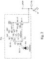
- Fig. 2 is a circuit diagram showing an example of a pixel according to the embodiment.
- the pixel PXL includes, for example, a photodiode PD1 serving as a photoelectric conversion part (a photoelectric conversion element).
- the pixel PXL includes one each of a transfer transistor TG1-Tr as a charge transfer gate part (a transfer element), a reset transistor RST1-Tr as a reset element, a source follower transistor SF1-Tr as a source follower element, a selection transistor SEL1-Tr as a selecting element, a storage transistor SG1-Tr as a storage element, and a storage capacitor CS1 as a storage capacitance element.
- the photodiode PD generates signal charges (electrons) in an amount in accordance with the quantity of the incident light and stores the same.
- signal charges electrons and each transistor is an n-type transistor.
- the signal charges are holes or each transistor is a p-type transistor.
- this embodiment is also applicable to the case where a plurality of photodiodes share the transistors or the case where the pixel includes four transistors (4Tr) other than the selection transistor.
- the photodiode (PD) in each pixel PXL is a pinned photodiode (PPD).
- PPD pinned photodiode
- a pinned photodiode (PPD) a charge storage part of the photodiode (PD) is pinned in the substrate to reduce mixing of the dark current into signals.
- the transfer transistor TG1-Tr is connected between the pinned photodiode (PPD) and a floating diffusion FD1 and controlled through a control signal TG.
- the transfer transistor TG1-Tr is selected and enters a conductive state in a period in which the control signal TG is at a high (H) level and transfers to the floating diffusion FD1 the charges (electrons) produced by photoelectric conversion and then stored in the photodiode PD1.
- the reset transistor RST1-Tr is connected between a power supply potential VDD and the storage transistor SG1-Tr connected to the floating diffusion FD1, and the reset transistor RST1-Tr is controlled through a control signal RST.
- the reset transistor RST1-Tr is selected and enters a conductive state in a period in which the control signal RST is at the H level and resets the floating diffusion FD1 to the power supply potential VDD when the storage transistor SG1-Tr is in a conductive state.
- the source of the storage transistor SG1-Tr is connected to the floating diffusion FD1.
- the storage capacitor CS1 is arranged such that the first electrode EL1 is connected to the reference potential VSS (e.g., the ground potential GND) and the second electrode EL2 is connected to the drain of the storage transistor SG1-Tr as a capacitance connection node ND1.
- the storage transistor SG1-Tr is controlled by the control signal SG applied to the gate thereof through the control line.
- the storage transistor SG1-Tr is selected and enters a conductive state in a period in which the control signal SG is at the H level and connects between the floating diffusion FD1 and the storage capacitor CS1.
- the first conversion gain (the high conversion gain: HCG) signal reading process is performed while the storage transistor SG1-Tr is maintained at a nonconductive state, such that the charges of the floating diffusion FD1 are separated from the charges of the storage capacitor CS1.
- the second conversion gain (the low conversion gain: LCG) signal reading process is performed while the storage transistor SG1-Tr is maintained at a conductive state, such that the charges of the floating diffusion FD1 and the charges of the storage capacitor CS1 are shared (mixed).
- the storage transistor SG1-Tr is connected between the floating diffusion FD1 and the reset transistor RST1-Tr, and the storage capacitor CS1 is connected between the connection node of the storage transistor SG1-Tr and the reference potential VSS.
- the reset transistor RST1-Tr and the storage transistor SG1-Tr may be individually in direct connection to the floating diffusion FD1.
- the source follower transistor SF1-Tr and the selection transistor SEL1-Tr are connected in series between the power supply potential VDD and a vertical signal line LSGN1 to which a current source IS is connected.
- the gate of the source follower transistor SF1-Tr is connected to the floating diffusion FD1, and the selection transistor SELl-Tr is controlled through a control signal SEL.
- the selection transistor SELl-Tr is selected and enters a conductive state in a period in which the control signal SEL is at the H level.
- the source follower transistor SF1-Tr outputs, to the vertical signal line LSGN1, a read-out signal VSL of a column output generated by converting the charges of the floating diffusion FD1 to a voltage signal with a gain corresponding to a quantity of the charges (the potential).
- These operations are performed in parallel for pixels in one row, because for example the gates of the transfer transistor TG1-Tr, the reset transistor RST1-Tr, the selection transistor SELl-Tr, and the storage transistor SG1-Tr are connected to each other in the unit of row.
- the control lines LSEL, LRST, LTG, LSG are represented as one row-scanning control line.
- the vertical scanning circuit 30 drives the pixels in shutter rows and reading rows through the row-scanning control lines in accordance with the control of the timing control circuit 60. Further, the vertical scanning circuit 30 outputs, according to address signals, row selection signals for row addresses of the reading rows from which signals are read out and the shutter rows in which the charges stored in the photodiodes PD1 are reset.
- the reading circuit 40 includes a plurality of column signal processing circuits (not shown) arranged corresponding to the column outputs of the pixel part 20, and the reading circuit 40 may be configured such that the plurality of column signal processing circuits can perform column parallel processing.
- the reading circuit 40 may include a correlated double sampling (CDS) circuit, an analog-digital converter (ADC), an amplifier (AMP), a sample/hold (S/H) circuit, and the like.
- CDS correlated double sampling
- ADC analog-digital converter
- AMP amplifier
- S/H sample/hold
- the reading circuit 40 may include ADCs 41 for converting the read-out signals VSL from the column outputs of the pixel part 20 into digital signals.
- the reading circuit 40 may include amplifiers (AMPs) 42 for amplifying the read-out signals VSL from the column outputs of the pixel part 20.
- the reading circuit 40 may include sample/hold (S/H) circuits 43 for sampling/holding the read-out signals VSL from the column outputs of the pixel part 20.
- the horizontal scanning circuit 50 scans the signals processed in the plurality of column signal processing circuits of the reading circuit 40 such as ADCs, transfers the signals in a horizontal direction, and outputs the signals to a signal processing circuit (not shown).
- the timing control circuit 60 generates timing signals required for signal processing in the pixel part 20, the vertical scanning circuit 30, the reading circuit 40, the horizontal scanning circuit 50, and the like.
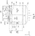
- Fig. 4 is a simplified sectional view showing an example configuration of the pixel according to the first embodiment of the present invention.
- the pixel described herein includes a pinned photodiode (PPD) and is denoted by a reference sign 200.
- PPD pinned photodiode
- the pixel 200 shown in Fig. 4 includes a semiconductor substrate (hereinafter referred to simply as "the substrate") 210 having a first substrate surface 211 side (e.g., a back surface side) to be irradiated with light L and a second substrate surface 212 side (a front surface side) opposed to the first substrate surface side 211.
- the substrate semiconductor substrate
- the pixel 200 includes: a photoelectric conversion part as a photodiode PD1 which includes a first conductivity type (n-type in this embodiment) semiconductor layer (n layer) 221 pinned in the substrate 210 and is configured to perform photoelectric conversion of received light and store charges; and a second conductivity type (p-type in this embodiment) semiconductor layer 230 formed at least on a side portion of the n layer (the first conductivity type semiconductor layer) 221 of the photoelectric conversion part 220.
- a photoelectric conversion part as a photodiode PD1 which includes a first conductivity type (n-type in this embodiment) semiconductor layer (n layer) 221 pinned in the substrate 210 and is configured to perform photoelectric conversion of received light and store charges
- a second conductivity type (p-type in this embodiment) semiconductor layer 230 formed at least on a side portion of the n layer (the first conductivity type semiconductor layer) 221 of the photoelectric conversion part 220.
- the pixel 200 includes: a transfer transistor TG1-Tr that transfers the charges stored in the photoelectric conversion part 220; a floating diffusion FD1 to which the charges are transferred through the transfer transistor TG1-Tr; and a storage transistor SG1-Tr with the source connected to the floating diffusion FD1; and a storage capacitor CS1 serving as a storage capacitance element that stores the charges received from the floating diffusion FD1 via the drain side of the storage transistor SG1-Tr.
- the storage capacitor CS1 serving as a storage capacitance element is formed on the second substrate surface 212 side so as to spatially overlap with the photoelectric conversion part 220 in the direction perpendicular to the substrate surface (the direction Z in the orthogonal coordinate system shown).
- the substrate 210 has a two-layer structure including a first region AR1 and a second region AR2 arranged in the direction perpendicular to the substrate surface (the direction Z in the orthogonal coordinate system shown).
- the first region AR1 has a first depth DP1 from the second substrate surface 212 toward the first substrate surface 211
- the second region AR2 has a second depth DP2 that is larger than the first depth DP1.
- the photoelectric conversion part 220 and the p layer (the second conductivity type semiconductor layer) 230 shown in Fig. 4 each have a two-layer structure in the direction perpendicular to the substrate surface of the substrate 210 (the direction Z in the orthogonal coordinate system shown).
- the photoelectric conversion part 220 has a two-layer structure including the n layer (the first conductivity type semiconductor layer) 221 in the second region AR2 and the n layer (the first conductivity type semiconductor layer) 222 in the first region AR1.
- the p layer (the second conductivity type semiconductor layer) 230 has a two-layer structure including the p layer (the second conductivity type semiconductor layer) 231 in the second region AR2 and the p layer (the second conductivity type semiconductor layer) 232 in the first region AR1.
- the photoelectric conversion part 220 includes a second conductivity type semiconductor region (a p+ region) 223 formed on the surface of the n layer (the first conductivity type semiconductor layer) 222 in the first region AR1 on the second substrate surface 212 side.
- the second conductivity type semiconductor region (the p+ region) 223 contains a higher concentration of impurities than the p layer (the second conductivity type semiconductor layer) 230 on the side portion of the n layer.
- the storage capacitor CS1 serving as a storage capacitance element uses, as a first electrode EL1 thereof, the p+ region (the second conductivity type semiconductor region) 223 formed in the surface on the second substrate surface 212 side.
- the storage capacitor CS1 serving as a storage capacitance element includes a first electrode EL1 and a second electrode EL2.
- the first electrode EL1 is formed of the p+ region (the second conductivity type semiconductor region) 223 formed in the surface of the second substrate surface 212 of the substrate 210, and the second electrode EL2 is formed above the second substrate surface 212 so as to be opposed at a distance to the first electrode EL1 in the direction perpendicular to the substrate surface.
- a flat layer 224 is formed on the surfaces of the n layer (the first conductivity type semiconductor layer) 221 of the photoelectric conversion part 220 and the p layer (the second conductivity type semiconductor layer) 230 on the first substrate surface 211 side.
- a color filter part CF is formed on the light incidence side of the flat layer 224, and further, a microlens MCL is formed on the light incidence side of the color filter part so as to correspond to the photoelectric conversion part 220 as the photodiode PD1 and the p layer (the second conductivity type semiconductor layer) 230.
- the p layer (the second conductivity type semiconductor layer) 232 in the first region AR1 contains the transfer transistor TG1-Tr, the floating diffusion FD1, and the storage transistor SG1-Tr.
- the floating diffusion FD1 is formed in the surface of the second substrate surface 212 of the substrate 210, so as to constitute an n+ region (the first conductivity type semiconductor region) 233 containing a higher concentration of impurities than the n layer (the first conductivity type semiconductor layer) 221, 222 of the photoelectric conversion part 220.
- the capacitance connection node ND1 of the storage transistor SG1-Tr for capacitance connection with the storage capacitor CS1 is formed in the surface of the second substrate surface 212 of the substrate 210, so as to constitute an n+ region (the first conductivity type semiconductor region) 234 containing a higher concentration of impurities than the n layers (the first conductivity type semiconductor layers) 221, 222 of the photoelectric conversion part 220.
- the n+ region 234 as the node ND1 is connected to the second electrode EL2 of the storage capacitor CS1 via a wiring layer WR1.
- the transfer transistor TG1-Tr includes a gate electrode 251 disposed above the second substrate surface 212 of the substrate 210 between the p+ region (the second conductivity type semiconductor region) 223 and the n+ region (the first conductivity type semiconductor region) 233 as the floating diffusion FD1.
- the storage transistor SG1-Tr includes a gate electrode 252 disposed above the second substrate surface 212 of the substrate 210 between the n+ region (the first conductivity type semiconductor region) 233 as the floating diffusion FD1 and the n+ region (the first conductivity type semiconductor region) 234 as the capacitance connection node ND1.
- the storage capacitor CS1 serving as a storage capacitance element includes the first electrode EL1 and the second electrode EL2 on the second substrate surface 212 side.
- the first electrode EL1 is formed of the p+ region (the second conductivity type semiconductor region) 223 formed in the surface of the second substrate surface 212 of the substrate 210, and the second electrode EL2 is formed above the second substrate surface 212 so as to be opposed at a distance to the first electrode EL1 in the direction perpendicular to the substrate surface.
- the first electrode EL1 and the second electrode EL2 are arranged so as to spatially overlap with the photoelectric conversion part 220 in the direction perpendicular to the substrate surface (the direction Z in the orthogonal coordinate system shown).
- the first embodiment implements both a wide dynamic range and a high sensitivity.
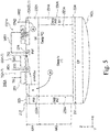
- Fig. 5 is a simplified sectional view showing an example configuration of the pixel according to the second embodiment of the present invention.
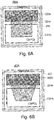
- Figs. 6A and 6B are plan views showing an example configuration of the pixel according to the second embodiment of the present invention.
- the pixel 200A of the second embodiment differs from the pixel 200 of the first embodiment (shown in Fig. 4 ) in the following points.
- the storage capacitor CS1 serving as a storage capacitance element includes the first electrode EL1 and the second electrode EL2 on the second substrate surface 212 side.
- the first electrode EL1 is formed of the p+ region (the second conductivity type semiconductor region) 223 formed in the surface of the second substrate surface 212 of the substrate 210, and the second electrode EL2 is formed above the second substrate surface 212 so as to be opposed at a distance to the first electrode EL1 in the direction perpendicular to the substrate surface.
- the first electrode EL1 and the second electrode EL2 are arranged so as to spatially overlap with the photoelectric conversion part 220 in the direction perpendicular to the substrate surface (the direction Z in the orthogonal coordinate system shown).
- the storage capacitor CS1A serving as a storage capacitance element which is formed on the second substrate surface 212 side so as to spatially overlap with the photoelectric conversion part 220 in the direction perpendicular to the substrate surface (the direction Z in the orthogonal coordinate system shown), has the following configuration.
- the pixel 200A is formed such that the area of the portion of the n layer (the first conductivity type semiconductor layer) 221A in the second region AR2 opposed to the second substrate surface 212 is larger than the area of the portion of the n layer (the first conductivity type semiconductor layer) 222A in the first region AR1 opposed to the second substrate surface 212.
- the n layer (the first conductivity type semiconductor layer) 221A in the second region AR2 extends in the direction X and the direction Y shown, and the n layer (the first conductivity type semiconductor layer) 222A in the first region AR1 is formed on an edge portion of the boundary region of the n layer (the first conductivity type semiconductor layer) 221A in the second region AR2.
- the first electrode EL1 of the storage capacitor CS1A serving as the storage capacitance element is formed in the surface of the second substrate surface 212 of the substrate 210, so as to be opposed to the portion of the surface of the n layer (the first conductivity type semiconductor layer) 221A in the second region AR2 on which the n layer (the first conductivity type semiconductor layer) 222A is absent, with the p layer (the second conductivity type semiconductor layer) 232A in the first region AR1 interposed therebetween.
- the first electrode EL1 constitutes a n+ region (the first conductivity type semiconductor region) 235 containing a higher concentration of impurities than the n layers 221A, 222A of the photoelectric conversion part 220A.
- the second electrode EL2 of the storage capacitor CS1A is formed above the second substrate surface 212 so as to be opposed at a distance to the first electrode EL1 in the direction perpendicular to the substrate surface.
- the storage capacitor CS1A is formed as a MOS capacitance.
- the first electrode EL1 is connected to the reference potential (the ground GND) through the wiring layer WR2.
- the first electrode EL1 of the storage capacitor CS1A is formed as the n+ region (the first conductivity type semiconductor region) 235 having a high concentration of impurities, and therefore, the capacitance density and the linearity can be increased.
- the n layer (the first conductivity type semiconductor layer) 222A in the first region AR1 is not opposed to the storage capacitor CS1A, electrons produced from a part of the incident light having a long wavelength photoelectrically converted in a shallow region are discharged through the substrate-side ground GND of the storage capacitor CS1A, and therefore, the sensitivity for long wavelengths may be lowered. This lowering of the sensitivity can be avoided by use of a thicker substrate and deeper ion injection for n-type and p-type.
- the n layer (the first conductivity type semiconductor layer) 222A in the first region AR1 is offset from the center of the pixel, and therefore, it is possible to increase the area efficiency of the storage capacitor CS1A, produce a larger capacitor, and enlarge the dynamic range.
- the electrons produced by the photoelectric conversion in the n layer (the first conductivity type semiconductor layer) 221A in the second region AR2 are transferred to and stored in the n layer (the first conductivity type semiconductor layer) 222A in the first region AR1 by the potential gradient through an overlap region with the n layer (the first conductivity type semiconductor layer) 222A in the first region AR1.
- the region for the n layer (the first conductivity type semiconductor layer) 221A in the second region AR2 can be reduced in size such that the area occupied by this region approximates the small area occupied by the n layer (the first conductivity type semiconductor layer) 222A.
- This arrangement makes it possible that the peak voltage position of the photoelectric conversion part 220 as the photodiode PD1 is formed in the n layer (the first conductivity type semiconductor layer) 222A in the first region AR1 and a transfer residue (a residual image) of the stored charges (the signals) is reduced.
- a large epitaxial (epi) region of p-type (the second conductivity type) may be intentionally left in the region allocated for forming the n layer (the first conductivity type semiconductor layer) 221A, so as to reduce the substantial region for the n layer (the first conductivity type semiconductor layer) 221A.
- the electrons produced by the photoelectric conversion in an epitaxial (epi) region between the n layer (the first conductivity type semiconductor layer) 221A in the second region AR2 and the p layer (the second conductivity type semiconductor layer) 231A in the second region AR2 are transferred to and stored in the n layer (the first conductivity type semiconductor layer) 222A in the first region AR1 by the potential gradient.
- the region for forming the n layer (the first conductivity type semiconductor layer) 221A in the second region AR2 may have such a shape that the electrons are readily transferred to the n layer (the first conductivity type semiconductor layer) 222A in the first region AR1, such as a trapezoidal shape or an L-shape, such that the electrons readily flow to the n layer (the first conductivity type semiconductor layer) 222A in the first region AR1.
- a trapezoidal shape or an L-shape such that the electrons readily flow to the n layer (the first conductivity type semiconductor layer) 222A in the first region AR1.
- the n layer (the first conductivity type semiconductor layer) 221A in the second region AR2 has a trapezoidal shape in plan view, the trapezoidal shape being wider toward the n layer (the first conductivity type semiconductor layer) 222A to which the electrons are transferred.
- Fig. 7 is a simplified sectional view showing an example configuration of the pixel according to the third embodiment of the present invention.
- the pixel 200B of the third embodiment differs from the pixel 200A of the second embodiment (shown in Fig. 5 ) in the following points.
- a p- region (a second conductivity type semiconductor region) 225 containing a low concentration of impurities is formed in a part of the n layer (the first conductivity type semiconductor layer) 222A in the first region AR1.
- This arrangement makes it possible that the peak voltage position of the photoelectric conversion part 220 as the photodiode PD1 is formed in the n layer (the first conductivity type semiconductor layer) 222A in the first region AR1 and a transfer residue (a residual image) of the stored charges (the signals) is reduced.
- a p- region (a second conductivity type semiconductor region) 226 containing a low concentration of impurities is formed in a part of the n layer (the first conductivity type semiconductor layer) 221A in the second region AR2.
- This arrangement makes it possible that the peak voltage position of the photoelectric conversion part 220 as the photodiode PD1 is formed in the n layer (the first conductivity type semiconductor layer) 222A in the first region AR1 and a transfer residue (a residual image) of the stored charges (the signals) is reduced.
- a large epitaxial (epi) region 227 of p-type is left between the n layer (the first conductivity type semiconductor layer) 221A in the second region AR2 and the p layer (the second conductivity type semiconductor layer) 231A in the second region AR2, such that the substantial region of the n layer (the first conductivity type semiconductor layer) 221A is small.
- This arrangement also makes it possible that the peak voltage position of the photoelectric conversion part 220 as the photodiode PD1 is formed in the n layer (the first conductivity type semiconductor layer) 222A in the first region AR1 and a transfer residue (a residual image) of the stored charges (the signals) is reduced.
- the electrons produced by the photoelectric conversion in an epitaxial (epi) region 227 between the n layer (the first conductivity type semiconductor layer) 221A in the second region AR2 and the p layer (the second conductivity type semiconductor layer) 231A in the second area AR2 are transferred to and stored in the n layer (the first conductivity type semiconductor layer) 222A in the first region AR1 by the potential gradient.
- Fig. 8 is a simplified sectional view showing an example configuration of the pixel according to the fourth embodiment of the present invention.
- the pixel 200C of the fourth embodiment differs from the pixel 200A of the second embodiment (shown in Fig. 5 ) in the following points.
- a p- region (a second conductivity type semiconductor region) 228 containing a low concentration of impurities is formed in a part of the n layer (the first conductivity type semiconductor layer) 222A in the first region AR1.
- This arrangement makes it possible that the peak voltage position of the photoelectric conversion part 220 as the photodiode PD1 is formed in the n layer (the first conductivity type semiconductor layer) 222A in the first region AR1 and a transfer residue (a residual image) of the stored charges (the signals) is reduced.
- the n layer (the first conductivity type semiconductor layer) 221A in the second region AR2 is formed such that the n layer regions 221A-2, 221A-3 on the first substrate surface 211 side are smaller than the n layer region 221A-1 contacting with the n layer (the first conductivity type semiconductor layer) 222A in the first region AR1. More specifically, the n layer regions 221A-2, 221A-3 on the first substrate surface 211 side are separated with an epitaxial (epi) region 227C of p-type disposed therebetween.
- This arrangement makes it possible that the peak voltage position of the photoelectric conversion part 220 as the photodiode PD1 is formed in the n layer (the first conductivity type semiconductor layer) 222A in the first region AR1 and a transfer residue (a residual image) of the stored charges (the signals) is reduced.
- the electrons produced by the photoelectric conversion in the n layers 221A-2, 221A-3 on the first substrate surface 211 side are transferred to and stored in the n layer (the first conductivity type semiconductor layer) 222A in the first region AR1 via the n layer region 221A-1.
- Fig. 9 is a simplified sectional view showing an example configuration of the pixel according to the fifth embodiment of the present invention.
- Fig. 9 focuses on the first region AR1 including modified or added parts and does not show the second region.
- the second region may be the same as that of the second, third, or fourth embodiment described above ( Figs. 5 to 8 ).
- the pixel 200D of the fifth embodiment differs from the pixel 200A of the second embodiment (shown in Fig. 5 ) in the following points.
- an n- region (a first conductivity type semiconductor region) 236 is formed on the second substrate surface 212 side under the gate electrode 252 of the storage transistor SG1-Tr so as to connect to the n+ region (the first conductivity type semiconductor region) 234 as the capacitance connection node ND1.
- the n- region (the first conductivity type semiconductor region) 236 contains a lower concentration of impurities than the n layers (the first conductivity type semiconductor layers) 221A, 222A of the photoelectric conversion part 220A.
- This arrangement forms the potential gradient under the gate electrode 252 of the storage transistor SG1-Tr, such that the charge injection occurring when the storage transistor SG1-Tr is switched off flows into the storage capacitor CS1A, instead of the floating diffusion FD1.
- the capacitance is smaller on the floating diffusion FD1 side to implement a higher sensitivity, while the capacitance is larger on the storage capacitor CS1 side to implement higher saturation, and therefore, the charge injection converted into a voltage is small, and it is possible to expand the full scale of signals and lower the voltages.
- the pixel 200D is of a shared pixel design in which the floating diffusion FD1 is shared by a plurality of photoelectric conversion parts 220 and a plurality of transfer transistors TG1-Tr, it is possible that, as shown by the broken line in Fig.
- an n- region (a first conductivity type semiconductor region) 237 is formed on the second substrate surface 212 side under the gate electrode 252 of the storage transistor SG1-Tr so as to connect to the n+ region (the first conductivity type semiconductor region) 233 as the FD node, and the n- region (the first conductivity type semiconductor region) 237 contains a lower concentration of impurities than the n layers (the first conductivity type semiconductor layers) 221A, 222A of the photoelectric conversion part 220A.
- the n+ region (the first conductivity type semiconductor region) 233 as the FD node can be reset prior to reading the signals, and therefore, an n- material containing a lower concentration of impurities is injected on the floating diffusion FD1 side under the gate electrode 251 of the storage transistor SG1-Tr.
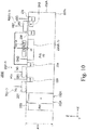
- Fig. 10 is a simplified sectional view showing an example configuration of the pixel according to the sixth embodiment of the present invention.
- Fig. 10 focuses on the first region AR1 including modified or added parts and does not show the second region.
- the second region may be the same as that of the second, third, or fourth embodiment described above ( Figs. 5 to 8 ).
- the pixel 200E of the sixth embodiment differs from the pixel 200A of the second embodiment (shown in Fig. 5 ) in the following points.
- the pixel 200E of the sixth embodiment includes the reset transistor RST1-Tr.
- the storage transistor SG1-Tr is connected between the floating diffusion FD1 and the reset transistor RST1-Tr, and the storage capacitor CS1A is connected between the connection node of the storage transistor SG1-Tr and the reference potential VSS.
- connection node connecting the reset transistor RST1-Tr to the storage capacitor CS1A and the storage transistor SG1-Tr (and further to the floating diffusion FD1) is formed in the surface of the second substrate surface 212 of the substrate 210 to constitute an n+ region (the first conductivity type semiconductor region) 238 containing a higher concentration of impurities than the n layers (the first conductivity type semiconductor layers) 221A, 222A of the photoelectric conversion part 220A.
- the power supply connection node connecting the reset transistor RST1-Tr to the power supply potential VDD is formed in the surface of the second substrate surface 212 of the substrate 210 to constitute an n+ region (the first conductivity type semiconductor region) 239 containing a higher concentration of impurities than the n layers (the first conductivity type semiconductor layers) 221A, 222A of the photoelectric conversion part 220A.
- the reset transistor RST1-Tr includes a gate electrode 253 disposed above the second substrate surface 212 of the substrate 210 between the n+ region (the first conductivity type semiconductor region) 238 as the connection node and the n+ region (the first conductivity type semiconductor region) 239 as the power supply connection node.
- an n- region (a first conductivity type semiconductor region) 240 is formed on the second substrate surface 212 side under the gate electrode 253 of the reset transistor RST1-Tr so as to connect to the n+ region (the first conductivity type semiconductor region) 239 as the power supply connection node.
- the n- region (the first conductivity type semiconductor region) 240 contains a lower concentration of impurities than the n layers (the first conductivity type semiconductor layers) 221A, 222A of the photoelectric conversion part 220A.
- the n- region (the first conductivity type semiconductor region) 240 containing a lower concentration of impurities is formed on the second substrate surface 212 side under the gate electrode 253 of the reset transistor RST1-Tr so as to connect to the n+ region (the first conductivity type semiconductor region) 239 as the power supply connection node.
- This arrangement forms the potential gradient under the gate electrode 253, such that the charge injection occurring when the reset transistor RST1-Tr is switched off flows into the power supply potential VAA, instead of the storage capacitor CS1A (or the floating diffusion FD1). As a result, the charge injection is small, and it is possible to expand the full scale of signals and lower the voltages.
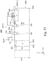
- Fig. 11 is a simplified sectional view showing an example configuration of the pixel according to the seventh embodiment of the present invention.
- Fig. 11 focuses on the first region AR1 including modified or added parts and does not show the second region.
- the second region may be the same as that of the second, third, or fourth embodiment described above ( Figs. 5 to 8 ).
- the pixel 200F of the seventh embodiment differs from the pixel 200A of the second embodiment (shown in Fig. 5 ) in that the storage capacitor CS1A is isolated by an STI (shallow trench isolation) 241.
- STI shallow trench isolation
- the seventh embodiment it is possible to reduce the dark current leaking from the first electrode EL1 to the second electrode EL2 of the storage capacitor CS1A via the n+ region (the first conductivity type semiconductor region) 234.
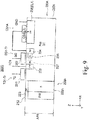
- Fig. 12A is a plan view showing an example configuration of the pixel according to the eighth embodiment of the present invention
- Fig. 12B is a simplified sectional view showing the same.
- the pixel 200G of the eighth embodiment differs from the pixel 200A of the second embodiment (shown in Fig. 5 ) in the following points.
- a p+ region (a second conductivity type semiconductor region) 242 for device isolation is formed in at least a surface portion on the second substrate surface 212 side between the n+ region (the first conductivity type semiconductor region) 235 as the first electrode EL1 of the storage capacitor CS1A and the n+ region (the first conductivity type semiconductor region) 234 as the capacitance connection node of the storage transistor SG1-Tr.
- the p+ region (a second conductivity type semiconductor region) 242 contains a higher concentration of impurities than the p layer (the second conductivity type semiconductor layer) 230 in a side portion. This arrangement reduces the dark current leaking from the first electrode EL1 to the second electrode EL2 of the storage capacitor CS1A via the n+ region (the first conductivity type semiconductor region) 234.
- a p-region (a second conductivity type semiconductor region) 243 containing a low concentration of impurities is formed between the n+ region (the first conductivity type semiconductor region) 233 as the floating diffusion FD1 and the p+ region (the second conductivity type semiconductor region) 242 for device isolation.
- This arrangement reduces the junction capacitance of the n+ region (the first conductivity type semiconductor region) 233 as the floating diffusion FD1 and improves the conversion and sensitivity.
- a p region (a second conductivity type semiconductor region) 244 is formed in a region between the n+ region (the first conductivity type semiconductor region) 233 as the floating diffusion FD1 and the n+ region (the first conductivity type semiconductor region) 234 as the capacitance connection node and deeper from the surface of the second substrate surface 212 than these n+ regions (the first conductivity type semiconductor regions) 233, 234. This arrangement reduces the parasitic light sensitivity.
- ring parts 245, 246 for limiting active regions surround the n+ region (the first conductivity type semiconductor region) 233 as the floating diffusion FD1 and the n+ region (the first conductivity type semiconductor region) 234 as the capacitance connection node. Narrowing the active regions makes it possible that the electrons produced by the photoelectric conversion in a shallow region of a part of incident light having a long wavelength are transferred to the source and/or the drain of the storage transistor so as to reduce the parasitic light sensitivity.
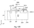
- Fig. 13A is a plan view showing an example configuration of the pixel according to the ninth embodiment of the present invention
- Fig. 13B is a simplified sectional view showing the same.
- Fig. 13B focuses on the first region AR1 including modified or added parts and does not show the second region.
- the second region may be the same as that of the second, third, or fourth embodiment described above ( Figs. 5 to 8 ).
- the pixel 200H of the ninth embodiment differs from the pixel 200E of the sixth embodiment (shown in Fig. 10 ) in the following points.
- the storage capacitor CS1A is isolated by an STI (shallow trench isolation) 241.
- the gate electrode 253 of the reset transistor RST1-Tr is surrounded by a ring part 247 for limiting the n+ region so as to narrow the region for injecting n-type ions, such that the STI and the n+ region 235 of the storage capacitor CS1A are isolated from each other by injection of p-type ions.
- the dark current occurring from the STI interface is not stored in the storage capacitor CS1A, thus reducing the noise.
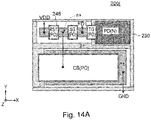
- Fig. 14A is a plan view showing an example configuration of the pixel according to the tenth embodiment of the present invention
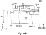
- Fig. 14B is a simplified sectional view showing the same.
- Fig. 14B focuses on the first region AR1 including modified or added parts and does not show the second region.
- the second region may be the same as that of the second, third, or fourth embodiment described above ( Figs. 5 to 8 ).
- the pixel 2001 of the tenth embodiment differs from the pixel 200E of the sixth embodiment (shown in Fig. 10 ) and the pixel 200H of the ninth embodiment (shown in Figs. 13A and 13B ) in the following points.
- the source (on the CS side) of the reset transistor RST1-Tr and the drain (on the CS side) and the source (FD) of the storage transistor SG1-Tr are isolated by a p-type injection layer (a p+ layer) 248.
- a p+ layer a p+ layer
- a p+ layer (a second conductivity type semiconductor region) 248 for device isolation is formed in at least a surface portion on the second substrate surface 212 side between the n+ region (the first conductivity type semiconductor region) 235 as the first electrode EL1 of the storage capacitor CS1A and the n+ region (the first conductivity type semiconductor region) 233 (not shown in Figs. 14A and 14B ) as the floating diffusion FD1.
- the n+ layer 238 serves as both the source (on the CS side) of the reset transistor RST1-Tr and the drain (on the CS side) of the storage transistor SG1-Tr. This arrangement is optional.
- Fig. 15 is a simplified sectional view showing an example configuration of the pixel according to the eleventh embodiment of the present invention.
- the pixel 200J of the eleventh embodiment differs from the pixel 200 of the first embodiment (shown in Fig. 4 ) in the following points.
- the pixel 200J of the eleventh embodiment includes an overflow path 261 for overflow charges in the photodiode PD1.
- the overflow path 261 is positioned directly below the transfer transistor TG1-Tr, the n+ region (the first conductivity type semiconductor region) 233 as the floating diffusion FD1, the storage transistor SG1-Tr, and the n+ region (the first conductivity type semiconductor region) 234 as the capacitance connection node ND1.
- the overflow path 261 is formed of, for example, an n-type (first conductivity type) pinned layer. More specifically, the overflow path 261 is formed as, for example, an n-type (first conductivity type) embedded layer positioned in a region deeper from the surface of the second substrate surface 212 than a p region (a second conductivity type semiconductor region) 232TG as a channel formation region for the transfer transistor TG1-Tr, the n+ region (the first conductivity type semiconductor region) 233 as the floating diffusion FD1, a p region (a second conductivity type semiconductor region) 232SG as a channel formation region for the storage transistor SG1-Tr, and the n+ region (the first conductivity type semiconductor region) 234 as the capacitance connection node ND1, each formed in the surface of the second substrate surface 212.
- the transfer transistor TG1-Tr and the storage transistor SG1-Tr are maintained at a gate potential of, for example, -1 V and enter the accumulation (storage) state. In this state, dark current charges occurring at a silicon interface are suppressed, and charges over the saturation charge are transferred to the floating diffusion FD1 and the storage capacitor CS1 as an overflow capacitor via the overflow path 261 without blooming to adjacent pixels and other elements.
- Fig. 16 shows a potential profile of a section under the transfer transistor of the pixel according to the eleventh embodiment during storage of charges.
- the overflow path 261 is configured to optimize the n-type dopant concentration and the thickness of the embedded layer such that it is formed at a sufficient depth directly below an interface under the transfer transistor TG1-Tr to reduce the dark current.
- Fig. 17 is a simplified sectional view showing an example configuration of the pixel according to the twelfth embodiment of the present invention.
- the pixel 200K of the twelfth embodiment differs from the pixel 200A of the second embodiment (shown in Fig. 5 ) in the following points.
- the pixel 200K of the twelfth embodiment includes an overflow path 262 for overflow charges in the photodiode PD1.
- the overflow path 262 is positioned directly below the transfer transistor TG1-Tr, the n+ region (the first conductivity type semiconductor region) 233 as the floating diffusion FD1, the storage transistor SG1-Tr, and the n+ region (the first conductivity type semiconductor region) 234 as the capacitance connection node.
- the overflow path 262 is formed of, for example, an n-type (first conductivity type) pinned layer. More specifically, the overflow path 262 is formed as, for example, an n-type (first conductivity type) embedded layer positioned in a region deeper from the surface of the second substrate surface 212 than a p region (a second conductivity type semiconductor region) 232TG as a channel formation region for the transfer transistor TG1-Tr, the n+ region (the first conductivity type semiconductor region) 233 as the floating diffusion FD1, a p region (a second conductivity type semiconductor region) 232SG as a channel formation region for the storage transistor SG1-Tr, and the n+ region (the first conductivity type semiconductor region) 234 as the capacitance connection node ND1, each formed in the surface of the second substrate surface 212.
- the transfer transistor TG1-Tr and the storage transistor SG1-Tr are maintained at a gate potential of, for example, -1 V and enter the accumulation (storage) state. In this state, dark current charges occurring at a silicon interface are suppressed, and charges over the saturation charge are transferred to the floating diffusion FD1 and the storage capacitor CS1 as an overflow capacitor via the overflow path 262 without blooming to adjacent pixels and other elements.
- the overflow path 262 is configured to optimize the n-type dopant concentration and the thickness of the embedded layer such that it is formed at a sufficient depth directly below an interface under the transfer transistor TG1-Tr to reduce the dark current.
- the solid-state imaging device 10 of the embodiment is applicable to a backside illumination (BSI) image sensor.
- BSI backside illumination
- the solid-state imaging device 10 described above can be applied, as an imaging device, to electronic apparatuses such as digital cameras, video cameras, mobile terminals, surveillance cameras, and medical endoscope cameras.
- Fig. 18 shows an example configuration of an electronic apparatus including a camera system to which the solid-state imaging device according to the embodiments of the present invention is applied.
- the electronic apparatus 300 includes a CMOS image sensor 310 that can be constituted by the solid-state imaging device 10 according to the embodiments of the present invention. Further, the electronic apparatus 300 includes an optical system (such as a lens) 320 for redirecting the incident light to pixel regions of the CMOS image sensor 310 (to form a subject image). The electronic apparatus 300 includes a signal processing circuit (PRC) 330 for processing output signals of the CMOS image sensor 310.
- PRC signal processing circuit
- the signal processing circuit 330 performs predetermined signal processing on the output signals of the CMOS image sensor 310.
- the image signals processed in the signal processing circuit 330 can be handled in various manners.
- the image signals can be displayed as a video image on a monitor having a liquid crystal display, or the image signals can be printed by a printer or recorded directly on a storage medium such as a memory card.
- a high-performance, compact, and low-cost camera system can be provided that includes the solid-state imaging device 10 as the CMOS image sensor 310. Further, it is possible to produce electronic apparatuses such as surveillance cameras and medical endoscope cameras that are used for applications where cameras are required to be installed under restricted conditions such as the installation size, number of connectable cables, cable length, and installation height.
Landscapes
- Engineering & Computer Science (AREA)
- Multimedia (AREA)
- Signal Processing (AREA)
- Solid State Image Pick-Up Elements (AREA)
- Transforming Light Signals Into Electric Signals (AREA)
Applications Claiming Priority (1)
| Application Number | Priority Date | Filing Date | Title |
|---|---|---|---|
| JP2018134131 | 2018-07-17 |
Publications (3)
| Publication Number | Publication Date |
|---|---|
| EP3598501A2 true EP3598501A2 (fr) | 2020-01-22 |
| EP3598501A3 EP3598501A3 (fr) | 2020-01-29 |
| EP3598501B1 EP3598501B1 (fr) | 2022-06-01 |
Family
ID=67437845
Family Applications (1)
| Application Number | Title | Priority Date | Filing Date |
|---|---|---|---|
| EP19186765.4A Active EP3598501B1 (fr) | 2018-07-17 | 2019-07-17 | Dispositif d'imagerie à semi-conducteur, procédé de fabrication d'un dispositif d'imagerie à semi-conducteur et appareil électronique |
Country Status (4)
| Country | Link |
|---|---|
| EP (1) | EP3598501B1 (fr) |
| JP (1) | JP7455525B2 (fr) |
| CN (1) | CN110729317B (fr) |
| TW (1) | TWI725484B (fr) |
Cited By (5)
| Publication number | Priority date | Publication date | Assignee | Title |
|---|---|---|---|---|
| WO2021234423A1 (fr) * | 2020-05-21 | 2021-11-25 | Sony Semiconductor Solutions Corporation | Structures capacitives pour dispositifs d'imagerie et appareils d'imagerie |
| EP4213492A1 (fr) * | 2022-01-17 | 2023-07-19 | Brillnics Singapore Pte. Ltd. | Dispositif d'imagerie à semi-conducteurs, procédé de commande de dispositif d'imagerie à semi-conducteurs et appareil électronique |
| US12328865B2 (en) | 2021-11-24 | 2025-06-10 | Samsung Electronics Co., Ltd. | Semiconductor device and method of fabricating the same |
| CN120813084A (zh) * | 2025-09-05 | 2025-10-17 | 荣芯半导体(宁波)有限公司 | 一种图像传感器及其制备方法 |
| US12495629B2 (en) | 2020-02-20 | 2025-12-09 | Semiconductor Energy Laboratory Co., Ltd. | Imaging device, electronic device, and moving object |
Families Citing this family (8)
| Publication number | Priority date | Publication date | Assignee | Title |
|---|---|---|---|---|
| KR102785835B1 (ko) * | 2020-05-25 | 2025-03-26 | 에스케이하이닉스 주식회사 | 이미지 센싱 장치 |
| CN114374805A (zh) * | 2020-10-14 | 2022-04-19 | 深圳市鸿飞精密科技有限公司 | 图像传感器及电子设备 |
| JP7656469B2 (ja) | 2021-04-05 | 2025-04-03 | ブリルニクス シンガポール プライベート リミテッド | 固体撮像装置、固体撮像装置の駆動方法、および電子機器 |
| KR20220152457A (ko) * | 2021-05-07 | 2022-11-16 | 삼성전자주식회사 | 이미지 센서 및 그 동작 방법 |
| JP2024010357A (ja) * | 2022-07-12 | 2024-01-24 | ブリルニクス シンガポール プライベート リミテッド | 固体撮像装置、固体撮像装置の駆動方法、および電子機器 |
| CN115732523B (zh) * | 2022-11-30 | 2026-03-17 | 南京威派视半导体技术有限公司 | 基于复合介质栅的背照式感光阵列及其成像装置 |
| WO2025169620A1 (fr) * | 2024-02-09 | 2025-08-14 | ソニーセミコンダクタソリューションズ株式会社 | Dispositif de détection de lumière et appareil électronique |
| JP7849543B1 (ja) * | 2025-04-28 | 2026-04-21 | タワー パートナーズ セミコンダクター株式会社 | 固体撮像素子 |
Citations (2)
| Publication number | Priority date | Publication date | Assignee | Title |
|---|---|---|---|---|
| JP2005223681A (ja) | 2004-02-06 | 2005-08-18 | Olympus Corp | 固体撮像装置 |
| JP4317115B2 (ja) | 2004-04-12 | 2009-08-19 | 国立大学法人東北大学 | 固体撮像装置、光センサおよび固体撮像装置の動作方法 |
Family Cites Families (31)
| Publication number | Priority date | Publication date | Assignee | Title |
|---|---|---|---|---|
| JPH05347401A (ja) * | 1992-06-15 | 1993-12-27 | Matsushita Electron Corp | 固体撮像素子 |
| JP3918220B2 (ja) * | 1997-02-27 | 2007-05-23 | ソニー株式会社 | 半導体装置及びその製造方法 |
| US6476426B1 (en) * | 1999-07-06 | 2002-11-05 | Motorola, Inc. | Electronic component and method for improving pixel charge transfer in the electronic component |
| JP2002050753A (ja) * | 2000-08-04 | 2002-02-15 | Innotech Corp | 固体撮像素子、その製造方法及び固体撮像装置 |
| JP3655542B2 (ja) * | 2000-09-22 | 2005-06-02 | 株式会社東芝 | 固体撮像装置 |
| US7071505B2 (en) * | 2003-06-16 | 2006-07-04 | Micron Technology, Inc. | Method and apparatus for reducing imager floating diffusion leakage |
| US7153738B2 (en) * | 2005-05-19 | 2006-12-26 | International Business Machines Corporation | Method for making a trench memory cell |
| JP4467542B2 (ja) * | 2006-06-15 | 2010-05-26 | 日本テキサス・インスツルメンツ株式会社 | 固体撮像装置 |
| EP1887626A1 (fr) * | 2006-08-09 | 2008-02-13 | Tohoku University | Capteur optique à grille de débordement et condensateur de stockage |
| US8101978B2 (en) * | 2008-02-08 | 2012-01-24 | Omnivision Technologies, Inc. | Circuit and photo sensor overlap for backside illumination image sensor |
| US20090201400A1 (en) * | 2008-02-08 | 2009-08-13 | Omnivision Technologies, Inc. | Backside illuminated image sensor with global shutter and storage capacitor |
| JP5213501B2 (ja) * | 2008-04-09 | 2013-06-19 | キヤノン株式会社 | 固体撮像装置 |
| JP4752926B2 (ja) * | 2009-02-05 | 2011-08-17 | ソニー株式会社 | 固体撮像装置、固体撮像装置の製造方法、固体撮像装置の駆動方法、電子機器 |
| JP5257176B2 (ja) * | 2009-03-18 | 2013-08-07 | ソニー株式会社 | 固体撮像装置、固体撮像装置の駆動方法および電子機器 |
| JP5505709B2 (ja) * | 2010-03-31 | 2014-05-28 | ソニー株式会社 | 固体撮像素子およびその製造方法、並びに電子機器 |
| JP5682150B2 (ja) * | 2010-06-14 | 2015-03-11 | ソニー株式会社 | 固体撮像素子及びその製造方法、撮像装置 |
| JP2012199489A (ja) * | 2011-03-23 | 2012-10-18 | Sony Corp | 固体撮像装置、固体撮像装置の製造方法、及び電子機器 |
| JP2013110285A (ja) * | 2011-11-22 | 2013-06-06 | Sony Corp | 固体撮像素子および製造方法、並びに、電子機器 |
| US8957359B2 (en) * | 2012-10-12 | 2015-02-17 | Omnivision Technologies, Inc. | Compact in-pixel high dynamic range imaging |
| US11322533B2 (en) * | 2013-03-14 | 2022-05-03 | Sony Semiconductor Solutions Corporation | Solid state image sensor tolerant to misalignment and having a high photoelectric conversion efficiency |
| US8835211B1 (en) * | 2013-05-24 | 2014-09-16 | Omnivision Technologies, Inc. | Image sensor pixel cell with global shutter having narrow spacing between gates |
| JP2015103735A (ja) * | 2013-11-27 | 2015-06-04 | ソニー株式会社 | 固体撮像素子および電子機器 |
| JP2015213274A (ja) * | 2014-05-07 | 2015-11-26 | ソニー株式会社 | 固体撮像装置、固体撮像装置の駆動方法、及び、電子機器 |
| US9613916B2 (en) * | 2015-03-12 | 2017-04-04 | Taiwan Semiconductor Manufacturing Co., Ltd. | Protection ring for image sensors |
| US9729810B2 (en) * | 2015-03-23 | 2017-08-08 | Tower Semiconductor Ltd. | Image sensor pixel with memory node having buried channel and diode portions |
| GB2537421A (en) * | 2015-04-17 | 2016-10-19 | Stmicroelectronics (Research & Development) Ltd | A pixel having a plurality of photodiodes |
| FR3037440B1 (fr) * | 2015-06-12 | 2019-11-08 | Teledyne E2V Semiconductors Sas | Capteur d'image a haute dynamique, a nœud de stockage en trois parties |
| JP6873905B2 (ja) * | 2015-09-11 | 2021-05-19 | ソニーセミコンダクタソリューションズ株式会社 | 固体撮像装置および電子機器 |
| JP6799739B2 (ja) * | 2016-03-30 | 2020-12-16 | 株式会社ブルックマンテクノロジ | 光検出素子及び固体撮像装置 |
| JPWO2017169882A1 (ja) * | 2016-03-31 | 2019-02-14 | ソニー株式会社 | 撮像素子、撮像素子の製造方法、及び、電子機器 |
| KR102638779B1 (ko) * | 2017-01-03 | 2024-02-22 | 삼성전자주식회사 | 이미지 센서 |
-
2019
- 2019-07-16 JP JP2019130986A patent/JP7455525B2/ja active Active
- 2019-07-17 CN CN201910647131.1A patent/CN110729317B/zh active Active
- 2019-07-17 EP EP19186765.4A patent/EP3598501B1/fr active Active
- 2019-07-17 TW TW108125329A patent/TWI725484B/zh active
Patent Citations (2)
| Publication number | Priority date | Publication date | Assignee | Title |
|---|---|---|---|---|
| JP2005223681A (ja) | 2004-02-06 | 2005-08-18 | Olympus Corp | 固体撮像装置 |
| JP4317115B2 (ja) | 2004-04-12 | 2009-08-19 | 国立大学法人東北大学 | 固体撮像装置、光センサおよび固体撮像装置の動作方法 |
Cited By (6)
| Publication number | Priority date | Publication date | Assignee | Title |
|---|---|---|---|---|
| US12495629B2 (en) | 2020-02-20 | 2025-12-09 | Semiconductor Energy Laboratory Co., Ltd. | Imaging device, electronic device, and moving object |
| WO2021234423A1 (fr) * | 2020-05-21 | 2021-11-25 | Sony Semiconductor Solutions Corporation | Structures capacitives pour dispositifs d'imagerie et appareils d'imagerie |
| US12328865B2 (en) | 2021-11-24 | 2025-06-10 | Samsung Electronics Co., Ltd. | Semiconductor device and method of fabricating the same |
| EP4213492A1 (fr) * | 2022-01-17 | 2023-07-19 | Brillnics Singapore Pte. Ltd. | Dispositif d'imagerie à semi-conducteurs, procédé de commande de dispositif d'imagerie à semi-conducteurs et appareil électronique |
| US12108182B2 (en) | 2022-01-17 | 2024-10-01 | Brillnics Singapore Pte. Ltd. | Solid-state imaging device, method for driving solid-state imaging device, and electronic apparatus |
| CN120813084A (zh) * | 2025-09-05 | 2025-10-17 | 荣芯半导体(宁波)有限公司 | 一种图像传感器及其制备方法 |
Also Published As
| Publication number | Publication date |
|---|---|
| CN110729317A (zh) | 2020-01-24 |
| TWI725484B (zh) | 2021-04-21 |
| JP7455525B2 (ja) | 2024-03-26 |
| TW202006961A (zh) | 2020-02-01 |
| JP2020017724A (ja) | 2020-01-30 |
| EP3598501B1 (fr) | 2022-06-01 |
| CN110729317B (zh) | 2022-06-14 |
| EP3598501A3 (fr) | 2020-01-29 |
Similar Documents
| Publication | Publication Date | Title |
|---|---|---|
| EP3598501B1 (fr) | Dispositif d'imagerie à semi-conducteur, procédé de fabrication d'un dispositif d'imagerie à semi-conducteur et appareil électronique | |
| US10462398B2 (en) | Solid-state imaging device, method of driving the same, and electronic apparatus | |
| KR101799262B1 (ko) | 촬상소자 및 촬상장치 | |
| US12108180B2 (en) | Solid-state imaging device, method for manufacturing solid-state imaging device, and electronic apparatus | |
| US10368019B2 (en) | Solid-state imaging device, method for driving solid-state imaging device, and electronic apparatus | |
| US8284282B2 (en) | Solid state imaging device, driving method of the solid state imaging device, and electronic equipment | |
| KR102499590B1 (ko) | 고체 촬상 소자 및 그 제조 방법, 및 전자 기기 | |
| JP6334203B2 (ja) | 固体撮像装置、および電子機器 | |
| JP2021097241A (ja) | 固体撮像素子および電子機器 | |
| CN108511471A (zh) | 固体摄像装置、固体摄像装置的制造方法以及电子设备 | |
| JP2015056878A (ja) | 固体撮像装置 | |
| US20210144319A1 (en) | Systems and methods for generating high dynamic range images | |
| KR20150002593A (ko) | 고체 촬상 장치 및 전자 기기 | |
| US12107095B2 (en) | Solid-state imaging device, method for fabricating solid-state imaging device, and electronic apparatus | |
| US12568322B2 (en) | Solid-state imaging device, method for manufacturing solid-state imaging device, and electronic apparatus | |
| US12108182B2 (en) | Solid-state imaging device, method for driving solid-state imaging device, and electronic apparatus | |
| JP2021068758A (ja) | 固体撮像装置、固体撮像装置の製造方法、および電子機器 | |
| JPH0965210A (ja) | 光電変換装置 | |
| WO2023087289A1 (fr) | Dispositif d'imagerie à semi-conducteurs et appareil électronique | |
| JP2017139498A (ja) | 固体撮像装置、および電子機器 | |
| JP2025114163A (ja) | 固体撮像装置、固体撮像装置の駆動方法、および電子機器 | |
| JPWO2016204225A1 (ja) | 固体撮像装置、固体撮像装置の駆動方法、および電子機器 |
Legal Events
| Date | Code | Title | Description |
|---|---|---|---|
| PUAI | Public reference made under article 153(3) epc to a published international application that has entered the european phase |
Free format text: ORIGINAL CODE: 0009012 |
|
| STAA | Information on the status of an ep patent application or granted ep patent |
Free format text: STATUS: THE APPLICATION HAS BEEN PUBLISHED |
|
| PUAL | Search report despatched |
Free format text: ORIGINAL CODE: 0009013 |
|
| AK | Designated contracting states |
Kind code of ref document: A2 Designated state(s): AL AT BE BG CH CY CZ DE DK EE ES FI FR GB GR HR HU IE IS IT LI LT LU LV MC MK MT NL NO PL PT RO RS SE SI SK SM TR |
|
| AX | Request for extension of the european patent |
Extension state: BA ME |
|
| AK | Designated contracting states |
Kind code of ref document: A3 Designated state(s): AL AT BE BG CH CY CZ DE DK EE ES FI FR GB GR HR HU IE IS IT LI LT LU LV MC MK MT NL NO PL PT RO RS SE SI SK SM TR |
|
| AX | Request for extension of the european patent |
Extension state: BA ME |
|
| RIC1 | Information provided on ipc code assigned before grant |
Ipc: H01L 27/146 20060101AFI20191220BHEP Ipc: H04N 5/335 20110101ALI20191220BHEP |
|
| STAA | Information on the status of an ep patent application or granted ep patent |
Free format text: STATUS: REQUEST FOR EXAMINATION WAS MADE |
|
| 17P | Request for examination filed |
Effective date: 20200729 |
|
| RBV | Designated contracting states (corrected) |
Designated state(s): AL AT BE BG CH CY CZ DE DK EE ES FI FR GB GR HR HU IE IS IT LI LT LU LV MC MK MT NL NO PL PT RO RS SE SI SK SM TR |
|
| RAP1 | Party data changed (applicant data changed or rights of an application transferred) |
Owner name: BRILLNICS SINGAPORE PTE. LTD. Owner name: TOHOKU TECHNO ARCH CO., LTD. |
|
| GRAP | Despatch of communication of intention to grant a patent |
Free format text: ORIGINAL CODE: EPIDOSNIGR1 |
|
| STAA | Information on the status of an ep patent application or granted ep patent |
Free format text: STATUS: GRANT OF PATENT IS INTENDED |
|
| RIC1 | Information provided on ipc code assigned before grant |
Ipc: H04N 5/3745 20110101ALI20211202BHEP Ipc: H04N 5/355 20110101ALI20211202BHEP Ipc: H01L 27/146 20060101AFI20211202BHEP |
|
| INTG | Intention to grant announced |
Effective date: 20211222 |
|
| GRAS | Grant fee paid |
Free format text: ORIGINAL CODE: EPIDOSNIGR3 |
|
| GRAA | (expected) grant |
Free format text: ORIGINAL CODE: 0009210 |
|
| STAA | Information on the status of an ep patent application or granted ep patent |
Free format text: STATUS: THE PATENT HAS BEEN GRANTED |
|
| AK | Designated contracting states |
Kind code of ref document: B1 Designated state(s): AL AT BE BG CH CY CZ DE DK EE ES FI FR GB GR HR HU IE IS IT LI LT LU LV MC MK MT NL NO PL PT RO RS SE SI SK SM TR |
|
| REG | Reference to a national code |
Ref country code: GB Ref legal event code: FG4D |
|
| REG | Reference to a national code |
Ref country code: AT Ref legal event code: REF Ref document number: 1495993 Country of ref document: AT Kind code of ref document: T Effective date: 20220615 Ref country code: CH Ref legal event code: EP Ref country code: DE Ref legal event code: R096 Ref document number: 602019015343 Country of ref document: DE |
|
| REG | Reference to a national code |
Ref country code: IE Ref legal event code: FG4D |
|
| REG | Reference to a national code |
Ref country code: NL Ref legal event code: FP |
|
| REG | Reference to a national code |
Ref country code: LT Ref legal event code: MG9D |
|
| PG25 | Lapsed in a contracting state [announced via postgrant information from national office to epo] |
Ref country code: SE Free format text: LAPSE BECAUSE OF FAILURE TO SUBMIT A TRANSLATION OF THE DESCRIPTION OR TO PAY THE FEE WITHIN THE PRESCRIBED TIME-LIMIT Effective date: 20220601 Ref country code: NO Free format text: LAPSE BECAUSE OF FAILURE TO SUBMIT A TRANSLATION OF THE DESCRIPTION OR TO PAY THE FEE WITHIN THE PRESCRIBED TIME-LIMIT Effective date: 20220901 Ref country code: LT Free format text: LAPSE BECAUSE OF FAILURE TO SUBMIT A TRANSLATION OF THE DESCRIPTION OR TO PAY THE FEE WITHIN THE PRESCRIBED TIME-LIMIT Effective date: 20220601 Ref country code: HR Free format text: LAPSE BECAUSE OF FAILURE TO SUBMIT A TRANSLATION OF THE DESCRIPTION OR TO PAY THE FEE WITHIN THE PRESCRIBED TIME-LIMIT Effective date: 20220601 Ref country code: GR Free format text: LAPSE BECAUSE OF FAILURE TO SUBMIT A TRANSLATION OF THE DESCRIPTION OR TO PAY THE FEE WITHIN THE PRESCRIBED TIME-LIMIT Effective date: 20220902 Ref country code: FI Free format text: LAPSE BECAUSE OF FAILURE TO SUBMIT A TRANSLATION OF THE DESCRIPTION OR TO PAY THE FEE WITHIN THE PRESCRIBED TIME-LIMIT Effective date: 20220601 Ref country code: ES Free format text: LAPSE BECAUSE OF FAILURE TO SUBMIT A TRANSLATION OF THE DESCRIPTION OR TO PAY THE FEE WITHIN THE PRESCRIBED TIME-LIMIT Effective date: 20220601 Ref country code: BG Free format text: LAPSE BECAUSE OF FAILURE TO SUBMIT A TRANSLATION OF THE DESCRIPTION OR TO PAY THE FEE WITHIN THE PRESCRIBED TIME-LIMIT Effective date: 20220901 |
|
| REG | Reference to a national code |
Ref country code: AT Ref legal event code: MK05 Ref document number: 1495993 Country of ref document: AT Kind code of ref document: T Effective date: 20220601 |
|
| PG25 | Lapsed in a contracting state [announced via postgrant information from national office to epo] |
Ref country code: RS Free format text: LAPSE BECAUSE OF FAILURE TO SUBMIT A TRANSLATION OF THE DESCRIPTION OR TO PAY THE FEE WITHIN THE PRESCRIBED TIME-LIMIT Effective date: 20220601 Ref country code: PL Free format text: LAPSE BECAUSE OF FAILURE TO SUBMIT A TRANSLATION OF THE DESCRIPTION OR TO PAY THE FEE WITHIN THE PRESCRIBED TIME-LIMIT Effective date: 20220601 Ref country code: LV Free format text: LAPSE BECAUSE OF FAILURE TO SUBMIT A TRANSLATION OF THE DESCRIPTION OR TO PAY THE FEE WITHIN THE PRESCRIBED TIME-LIMIT Effective date: 20220601 |
|
| PG25 | Lapsed in a contracting state [announced via postgrant information from national office to epo] |
Ref country code: SM Free format text: LAPSE BECAUSE OF FAILURE TO SUBMIT A TRANSLATION OF THE DESCRIPTION OR TO PAY THE FEE WITHIN THE PRESCRIBED TIME-LIMIT Effective date: 20220601 Ref country code: SK Free format text: LAPSE BECAUSE OF FAILURE TO SUBMIT A TRANSLATION OF THE DESCRIPTION OR TO PAY THE FEE WITHIN THE PRESCRIBED TIME-LIMIT Effective date: 20220601 Ref country code: RO Free format text: LAPSE BECAUSE OF FAILURE TO SUBMIT A TRANSLATION OF THE DESCRIPTION OR TO PAY THE FEE WITHIN THE PRESCRIBED TIME-LIMIT Effective date: 20220601 Ref country code: PT Free format text: LAPSE BECAUSE OF FAILURE TO SUBMIT A TRANSLATION OF THE DESCRIPTION OR TO PAY THE FEE WITHIN THE PRESCRIBED TIME-LIMIT Effective date: 20221003 Ref country code: EE Free format text: LAPSE BECAUSE OF FAILURE TO SUBMIT A TRANSLATION OF THE DESCRIPTION OR TO PAY THE FEE WITHIN THE PRESCRIBED TIME-LIMIT Effective date: 20220601 Ref country code: CZ Free format text: LAPSE BECAUSE OF FAILURE TO SUBMIT A TRANSLATION OF THE DESCRIPTION OR TO PAY THE FEE WITHIN THE PRESCRIBED TIME-LIMIT Effective date: 20220601 Ref country code: AT Free format text: LAPSE BECAUSE OF FAILURE TO SUBMIT A TRANSLATION OF THE DESCRIPTION OR TO PAY THE FEE WITHIN THE PRESCRIBED TIME-LIMIT Effective date: 20220601 |
|
| PG25 | Lapsed in a contracting state [announced via postgrant information from national office to epo] |
Ref country code: MC Free format text: LAPSE BECAUSE OF FAILURE TO SUBMIT A TRANSLATION OF THE DESCRIPTION OR TO PAY THE FEE WITHIN THE PRESCRIBED TIME-LIMIT Effective date: 20220601 Ref country code: IS Free format text: LAPSE BECAUSE OF FAILURE TO SUBMIT A TRANSLATION OF THE DESCRIPTION OR TO PAY THE FEE WITHIN THE PRESCRIBED TIME-LIMIT Effective date: 20221001 |
|
| REG | Reference to a national code |
Ref country code: DE Ref legal event code: R097 Ref document number: 602019015343 Country of ref document: DE |
|
| PG25 | Lapsed in a contracting state [announced via postgrant information from national office to epo] |
Ref country code: AL Free format text: LAPSE BECAUSE OF FAILURE TO SUBMIT A TRANSLATION OF THE DESCRIPTION OR TO PAY THE FEE WITHIN THE PRESCRIBED TIME-LIMIT Effective date: 20220601 |
|
| PLBE | No opposition filed within time limit |
Free format text: ORIGINAL CODE: 0009261 |
|
| STAA | Information on the status of an ep patent application or granted ep patent |
Free format text: STATUS: NO OPPOSITION FILED WITHIN TIME LIMIT |
|
| PG25 | Lapsed in a contracting state [announced via postgrant information from national office to epo] |
Ref country code: LU Free format text: LAPSE BECAUSE OF NON-PAYMENT OF DUE FEES Effective date: 20220717 Ref country code: DK Free format text: LAPSE BECAUSE OF FAILURE TO SUBMIT A TRANSLATION OF THE DESCRIPTION OR TO PAY THE FEE WITHIN THE PRESCRIBED TIME-LIMIT Effective date: 20220601 |
|
| 26N | No opposition filed |
Effective date: 20230302 |
|
| PG25 | Lapsed in a contracting state [announced via postgrant information from national office to epo] |
Ref country code: SI Free format text: LAPSE BECAUSE OF FAILURE TO SUBMIT A TRANSLATION OF THE DESCRIPTION OR TO PAY THE FEE WITHIN THE PRESCRIBED TIME-LIMIT Effective date: 20220601 |
|
| PG25 | Lapsed in a contracting state [announced via postgrant information from national office to epo] |
Ref country code: HU Free format text: LAPSE BECAUSE OF FAILURE TO SUBMIT A TRANSLATION OF THE DESCRIPTION OR TO PAY THE FEE WITHIN THE PRESCRIBED TIME-LIMIT; INVALID AB INITIO Effective date: 20190717 |
|
| PG25 | Lapsed in a contracting state [announced via postgrant information from national office to epo] |
Ref country code: MK Free format text: LAPSE BECAUSE OF FAILURE TO SUBMIT A TRANSLATION OF THE DESCRIPTION OR TO PAY THE FEE WITHIN THE PRESCRIBED TIME-LIMIT Effective date: 20220601 Ref country code: CY Free format text: LAPSE BECAUSE OF FAILURE TO SUBMIT A TRANSLATION OF THE DESCRIPTION OR TO PAY THE FEE WITHIN THE PRESCRIBED TIME-LIMIT Effective date: 20220601 |
|
| PG25 | Lapsed in a contracting state [announced via postgrant information from national office to epo] |
Ref country code: TR Free format text: LAPSE BECAUSE OF FAILURE TO SUBMIT A TRANSLATION OF THE DESCRIPTION OR TO PAY THE FEE WITHIN THE PRESCRIBED TIME-LIMIT Effective date: 20220601 |
|
| PG25 | Lapsed in a contracting state [announced via postgrant information from national office to epo] |
Ref country code: MT Free format text: LAPSE BECAUSE OF FAILURE TO SUBMIT A TRANSLATION OF THE DESCRIPTION OR TO PAY THE FEE WITHIN THE PRESCRIBED TIME-LIMIT Effective date: 20220601 |
|
| PG25 | Lapsed in a contracting state [announced via postgrant information from national office to epo] |
Ref country code: BG Free format text: LAPSE BECAUSE OF FAILURE TO SUBMIT A TRANSLATION OF THE DESCRIPTION OR TO PAY THE FEE WITHIN THE PRESCRIBED TIME-LIMIT Effective date: 20220601 |
|
| REG | Reference to a national code |
Ref country code: DE Ref legal event code: R079 Ref document number: 602019015343 Country of ref document: DE Free format text: PREVIOUS MAIN CLASS: H01L0027146000 Ipc: H10F0039180000 |
|
| PG25 | Lapsed in a contracting state [announced via postgrant information from national office to epo] |
Ref country code: BG Free format text: LAPSE BECAUSE OF FAILURE TO SUBMIT A TRANSLATION OF THE DESCRIPTION OR TO PAY THE FEE WITHIN THE PRESCRIBED TIME-LIMIT Effective date: 20220601 |
|
| PGFP | Annual fee paid to national office [announced via postgrant information from national office to epo] |
Ref country code: NL Payment date: 20250526 Year of fee payment: 7 |
|
| PGFP | Annual fee paid to national office [announced via postgrant information from national office to epo] |
Ref country code: GB Payment date: 20250529 Year of fee payment: 7 |
|
| PGFP | Annual fee paid to national office [announced via postgrant information from national office to epo] |
Ref country code: BE Payment date: 20250619 Year of fee payment: 7 |
|
| PGFP | Annual fee paid to national office [announced via postgrant information from national office to epo] |
Ref country code: FR Payment date: 20250618 Year of fee payment: 7 |
|
| PGFP | Annual fee paid to national office [announced via postgrant information from national office to epo] |
Ref country code: IE Payment date: 20250523 Year of fee payment: 7 |
|
| PGFP | Annual fee paid to national office [announced via postgrant information from national office to epo] |
Ref country code: DE Payment date: 20250521 Year of fee payment: 7 |
|
| PGFP | Annual fee paid to national office [announced via postgrant information from national office to epo] |
Ref country code: CH Payment date: 20250801 Year of fee payment: 7 |
|
| PGFP | Annual fee paid to national office [announced via postgrant information from national office to epo] |
Ref country code: IT Payment date: 20250623 Year of fee payment: 8 |